1411.3179
TRANSCRIPT
NStaley
Electric-field driven insulating to conducting transition in a mesoscopic quantum dotlattice
Neal E. Staley,∗ Nirat Ray, and Marc A. KastnerDepartment of Physics, Massachusetts Institute of Technology, Cambridge, Massachusetts 02139, U.S.A.
Micah P. Hanson and Arthur C. GossardMaterials Department, University of California, Santa Barbara, California 93106-5050, U.S.A
(Dated: November 13, 2014)
We investigate electron transport through a finite two dimensional mesoscopic periodic potential,consisting of an array of lateral quantum dots with electron density controlled by a global top gate.We observe a transition from an insulating state at low bias voltages to a conducting state at highbias voltages. The insulating state shows simply activated temperature dependence, with stronglygate voltage dependent activation energy. At low temperatures the transition between the insulatingand conducting states becomes very abrupt and shows strong hysteresis. The high-bias behaviorsuggests underdamped transport through a periodic washboard potential resulting from collectivemotion.
There has been great interest in understanding the mo-tion of charge carriers in artificial periodic potentials withmesoscopic periods[1–3]. In particular, one might betterunderstand transport in general by controlling the en-ergy scales of importance: For quantum transport in suchsystems the important energies are the on-site excitationand Coulomb charging energies and the inter-site tunnel-ing matrix element. Control of these energies has beendemonstrated in single lateral quantum dots connectedby tunneling to leads, leading to insights into the Kondoeffect[4], for example; similar insights into the Hubbardmodel might emerge from experiments on arrays of lat-eral quantum dots[5–7]. For classical transport modeledas charge diffusion through a tilted washboard potential,applicable to a wide variety of experimental systems[8–10], the energy scale is the height of the potential bar-rier between sites. In addition to the general question ofwhether quantum or classical transport dominates, ar-tificial periodic potentials may provide insights into theextensive work on self-assembled arrays of semiconductornanocrystals useful for opto-electronic devices[11, 12].
Many years ago, Duruoz et al. reported switchingand hysteresis in an array of 200 by 200 lateral quan-tum dots in GaAs/AlGaAs heterostructures[13]. Subse-quent experiments have been unable to reproduce theseeffects[14, 15], raising the possibility that the observedhysteresis results from the leakeage current between thegate and dots observed by Duruoz et al. In this Letter wereport detailed measurements of the current through a 10by 10 array of lateral quantum dots with a period of 340nm. Like Duruoz et al., we find a hysteretic transitionfrom a high resistance state at low bias to a low resistancestate at high bias which is strongly tuned by magneticfield. Unlike previous measurements our devices haveimmeasurably small leakage between the gate and thedot array. We have studied the temperature, magnetic
∗Electronic address: [email protected]
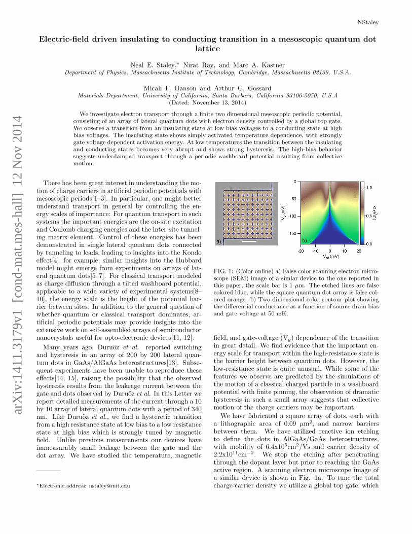
FIG. 1: (Color online) a) False color scanning electron micro-scope (SEM) image of a simlar device to the one reported inthis paper, the scale bar is 1 µm. The etched lines are falsecolored blue, while the square quantum dot array is false col-ored orange. b) Two dimensional color contour plot showingthe differential conductance as a function of source drain biasand gate voltage at 50 mK.
field, and gate-voltage (Vg) dependence of the transitionin great detail. We find evidence that the important en-ergy scale for transport within the high-resistance state isthe barrier height between quantum dots. However, thelow-resistance state is quite unusual. While some of thefeatures we observe are predicted by the simulations ofthe motion of a classical charged particle in a washboardpotential with finite pinning, the observation of dramatichysteresis in such a small array suggests that collectivemotion of the charge carriers may be important.
We have fabricated a square array of dots, each witha lithographic area of 0.09 µm2, and narrow barriersbetween them. We have utilized reactive ion etchingto define the dots in AlGaAs/GaAs heterostructures,with mobility of 6.4x105cm2/Vs and carrier density of2.2x1011cm−2. We stop the etching after penetratingthrough the dopant layer but prior to reaching the GaAsactive region. A scanning electron microscope image ofa similar device is shown in Fig. 1a. To tune the totalcharge-carrier density we utilize a global top gate, which
arX
iv:1
411.
3179
v1 [
cond
-mat
.mes
-hal
l] 1
2 N
ov 2
014

2
FIG. 2: (Color Online) Current vs voltage at temperaturesbetween 2 and 20K at Vg=-150 mV on a linear plot a) andsemi-log plot b). For each successive trace the temperature isincreased by 2K. The inset in a) shows the same traces plottedvs (V-VT ) c) and d ) are semi-log plots of the magnitude of thecurrent vs. source drain bias (solid red curve), with fits to thehigh bias power law (dashed green) and the low exponential(dashed blue) at two specific temperatures.
FIG. 3: (Color Online) a) The gate voltage dependence of thesingle particle gap. The single particle gap in zero magneticfield was extracted from the temperature dependence of thezero bias conductance (red circles) and from the fits to theI-V curves (blue triangles). The single particle gap at 9Textracted from I-V curves is shown as green diamonds. b) Plotshowing current voltage (I-V) hysteresis loops taken atVg=-240 mV for applied magnetic fields from 0T to 9T.
is isolated from the quantum dots by 100 nm of evapo-rated SiO2. The data presented here is measured using atwo terminal geometry, with contact resistances into thearray of <5kΩ, using both AC and DC techniques in adilution refrigerator with room temperature RF filteringand low temperature microwave filtering.
Measurements of our device at low temperatures re-veal a non-conducting to conducting transition driven by
source drain bias (V) that has a strong dependence onthe gate voltage (Vg). In Fig. 1b we show the differen-tial conductance as a function of Vg and V at 50 mK.At this temperature, for positive gate voltages, whichcorrespond to adding electrons into the array, we see acomponent with finite zero-bias conductance, but with azero-bias anomaly –a rapid increase of conductance withsmall bias. As we decrease the gate voltage, which beginsto deplete the array, the zero bias anomaly broadens andevolves, near Vg= -75 mV, into a non-conducting stateat V=0. At more negative Vg the current-voltage (I-V)characteristic has a distinct threshold for conduction anda power-law dependence above threshold. As Vg is mademore negative the threshold becomes abrupt. Very simi-lar behavior is seen for negative and positive V. Similarlyabrupt transitions from an insulating to conducting statein quantum dot arrays have been previously observed andattributed to leakage current between the top gate andthe array[13]. In our experiment, we observe no measur-able gate leakage with applied gate voltages up to -1.1V.
To better characterize the insulating-to-conductingtransition we have measured its temperature dependence.Shown in Fig. 2a are a series of I-V traces taken at tem-peratures from 2 to 20 K at Vg= -150 mV. In the log plotof the same data (Fig. 2b), one can clearly see both thelow bias non-conducting state and the high bias conduct-ing state, as well as the transition between the two, whichbecomes abrupt below 10 K. At temperatures below 2Kfor this Vg the current in the low bias state becomesimmeasurable. We see that at sufficiently high temper-atures there is finite conductivity at zero bias, whichfreezes out as we decrease the temperature, suggestingthat the non-conducting state is a gapped insulator. Incontrast, the high bias behavior shows only a weak tem-perature dependence of the threshold voltage up to 20K.Interestingly, the high bias curves collapse into a singletrace by shifting the voltage axis by the threshold voltageas shown in the inset of Fig. 2a. The slight deviationsfrom a single collapsed trace seen in at very high biasmight be due to electron self heating.
We find that a simple model describes the I-V charac-teristic of the array: At low V, the current is consistentwith that of thermally activated single particles overcom-ing a barrier,
I = V G0e−(∆−eV x/L)
kBT (1)
with an activation energy ∆ that is reduced by the fieldacross the barrier Vx/L, where L is the length of the arrayand x is width of the barrier. Well above the thresholdvoltage, VT , the current follows a power law,
I = C(V − VT )α (2)
Fits to both components are shown in Fig. 2c and d fortemperatures of 16.2 K and 10.2K, respectively, using thesame values of G0, x, ∆, C and α. From the low bias be-havior we can extract the characteristic length, x/L. Forthis array and gate voltage x/L=0.12±0.01, correspond-ing to x = 410±50 nm. As can be seen from Fig.2c,d,

3
FIG. 4: (Color Online) Semi-log plot of the magnitude current vs source drain bias at 50 mK for hysteresis loops taken every20 mV for gate voltages ranging from -160mV to -900mV. Note the strong hysteresis between gate voltages of -220 mV to -580mV, also note the splitting of the switching behavior which could indicate the formation of two distinct domains. Inset showsa single hysteresis loop taken at Vg=-300 mV plotted in a linear scale.
the exponentially voltage-dependent process should dom-inate, were it present at high bias voltages, but this is notobserved. Similarly, the power-law fit to the high-biascurrent, overestimates the current at low biases. Thusthe two transport processes do not add, suggesting thatthey compete with each other.
We measure ∆ from the temperature dependence ofthe zero-bias conductance and fits to the I-V characteris-tics. For low gate voltages and low magnetic fields wherethe device is weakly insulating, the zero-bias conductancemeasurements are used, while for high gate voltages theI-V characteristics are used. ∆ is strongly Vg dependent,increasing from 2.2 meV at a Vg= -60 mV, to 24.6 meVat a Vg= -350 mV as shown in Fig 3a. The activationenergy shows negligible dependence on an externally ap-plied magnetic field up to 9T as seen in Fig. 3a.
Perhaps the most striking feature of our data is theabruptness and the hysteresis associated with the tran-sition between the insulating and conducting states ob-served at temperatures below 10 K. At base temperature,this abrupt transition is extremely sharp, with currentjumps of more than three orders of magnitude observedat zero magnetic field. In a magnetic field the insulatingstate is strongly stabilized, making the hysteresis muchlarger, as shown in Fig. 3b, showing a 5 orders of magni-tude change between consecutive voltage points. Whatis remarkable is that the magnetic field both stabilisesthe insulating state and increases the conductance of theconducting state.
The abrupt transition between the insulating and con-ducting states exists over a large range of gate voltagesat base temperature as shown in Fig. 4. This transitionbecomes hysteretic near a gate voltage of -220 mV at zeromagnetic field. As we further deplete the array by mak-ing Vg more negative, the abrupt current step rapidlysaturates in amplitude until high gate voltages where weobserve additional transitions and a gradual decrease inhysteresis amplitude. For Vg more negative than ∼-700mV, no transitions are observed, and the power law expo-
nent becomes constant at ∼5.6. We expect that at suchlarge negative Vg the array is largly depleted of electrons.
To interpret our results we first note that the activationenergies we observe, especially at Vg more negative than∼-200 mV are much too large to be associated with thecharging energy of a single dot, which we estimate, fromthe lithographic dimensions, to be ∼3.5 meV. The tunnel-ing matrix element and on-site excitation energies are ex-pected to be even smaller. This and the dramatic increasein the activation energy with more negative Vg stronglysuggest that the high-resistance state is limited by ther-mal activation over the barrier between sites in the array.Thus, models like that of Middleton and Wingreen[16], inwhich the transport is limited by the Coulomb chargingenergy would seem to be excluded.
We next note that the multiple transitions seen, forexample, in Fig. 4, suggest that the sample contains anumber of domains, likely nucleated at disorder by dis-order within the array, that undergo the transition inde-pendently, once the barrier height is large. We have alsomade true 4 terminal measurements on a much larger19x39 array, and find qualitatively similar results. Wetherefore infer that in our geometry the high bias fieldtilts the washboard potential, reducing the barrier heightfor carrier motion down-field but leaving the barrierheight in the perpendicular direction unchanged, leavingeffectively ten rows of dots. It is therefore reasonable toassume that the transition occurs when the washboardpotential is tilted by a critical field. We find that thethreshold is roughly linear in gate voltage and the acti-vation energy (see Fig. 3) is linear in gate voltage, so thetransition appears to occur when the activation energyis reduced to a critical value near 10 meV. Disorder willthen cause different rows to undergo transitions at some-what different fields. We note, however, that there are farfewer transitions than rows of dots, indicating that thetransitions in adjacent rows are somewhat correlated.
Abrupt conductance changes have been previously ob-served in a wide variety of experimental systems resulting

4
from correlated[18, 19], or non-equilibrium[20] physics.In particular, for strongly temperature dependent sys-tems, thermal runaway can cause dramatic increases inthe conductivity as the source drain bias is increased[20].In our quantum dot arrays the measured activation en-ergies are so large that a temperature rise of over 15 Kwould be required to explain the switching at low tem-perature. One usually observes a considerable conduc-tance increase prior to run-away, and we see no such pre-cursor at low T and large negative Vg. Furthermore,the large change in hysteresis observed at high magneticfields, which does not influence the observed single par-ticle gap within the insulating state but dramatically in-creases the power dissipated in the device in the conduct-ing state strongly suggests this is not thermal runaway. Itis well-known that impact ionization or avalanche break-down can give rise to abrupt increases in current, as wellas hysteresis. While the electric fields where we observethe transitions are rather large, >150 V/cm, we wouldnot expect the observed temperature or magnetic fielddependence of the step transitions and hysteresis in sucha small system, were such mechanism responsible.
There has been a good deal of theoretical work on themotion of single classical charge carriers in an infinitewashboard potentia[21–23]. Our system can be thoughtof as a small section of such a potential. The simulationsshow that at low field the carriers are pinned in the po-tential wells in an insulating “stationary” state, with anactivation energy determined by the barrier height be-tween wells, while above a characteristic threshold field afraction of carriers are free to traverse the washboard ina conducting “running” state. Reference[23] claims that
there is hysteresis when the field is lowered. However, itseems likely that the hysteresis in the simulations is theresult of the infinite size of the system. It is difficult toimagine that for a system as small as ours, the runningstate could be sustained for the many minutes necessaryto yield the observed hysteresis.
Many of the features we see are reminiscent of the be-havior of charge-density waves (CDWs), which are de-scribed by motion of a classical particle in a tilted wash-board potential. In that case hysteresis arises from themomentum of the collective state, once the threshold forits motion is overcome. The power law I-V characteristicobserved at high biases, with an exponent of 2.3 differsfrom the CDW exponent of 3
2 [9], possibly due to the finitesample size or non-sinusoidal potential. Due to the hys-teresis and other features, we suggest that the high-fieldstate results from collective motion of the carriers in theperiodic potential. Experiments are planned to searchfor the narrow-band noise anticipated for such motion.
Acknowledgments
We acknowledge useful discussions with Prof. LeonidS. Levitov, Prof. Ivan Marchenko and Dr. William D.Oliver. The work at MIT was supported by the NSF un-der Grant DMR-1104394, the work at UC Santa Barbarawas supported by the NSEC Program of the NSF un-der Grant No. PHY-0117795. NR acknowledges supportfrom the Schlumberger Foundation through the Facultyfor the Future Fellowship Program.
[1] L. Esaki and R. Tsu, IBM Journal of Research and De-velopment 14, 61 (1970).
[2] D. J. Thouless, M. Kohmoto, M. P. Nightingale, andM. den Nijs, Physical Review Letters 49, 405 (1982).
[3] F. .M. Peeters and P. Vasilopoulos, Physical Review B46, 4667 (1992).
[4] D. Goldhaber-Gordon, H. Shtrikman, D. Mahalu,D. Abusch-Magder, U. Meirav, and M. A. Kastner, Na-ture 391, 156 (1998).
[5] T. Byrnes, N. Y. Kim, K. Kusudo, and Y. Yamamoto,Physical Review B 78, 075320 (2008).
[6] M. Nita, B. Ostahie, and A. Aldea, Physical Review B87, 125428 (2013).
[7] A. Singha, et al., Science 332, 1176 (2011).[8] M. Tinkham, Introduction to Superconductivity (Dover
Publications, Inc., 1996).[9] G. Gruner, Reviews of Modern Physics 60, 1129 (1988).
[10] G. Costantini and F. Marchesoni, EPL (Europhysics Let-ters) 48, 491 (1999).
[11] C. B. Murray, C. R. Kagan, and M. G. Bawendi, Science270, 1335 (1995).
[12] C. A. Leatherdale, C. R. Kagan, N. Y. Morgan,S. A. Empedocles, M. A. Kastner, and M. G. Bawendi,Physical Review B 62, 2669 (2000).
[13] C. I. Duruoz, R. M. Clarke, C. M. Marcus, and J. S. Har-
ris Jr, Physical Review Letters 74, 3237 (1995).[14] A. Dorn, T. Ihn, K. Ensslin, W. Wegscheider, and
M. Bichler, Physical Review B 70, 205306 (2004).[15] S. Goswami, M. A. Aamir, C. Siegert, M. Pepper, I. Far-
rer, D. A. Ritchie, and A. Ghosh, Physical Review B 85,075427 (2012).
[16] A. A. Middleton and N. S. Wingreen, Physical ReviewLetters 71, 3198 (1993).
[17] R. Parthasarathy, X.-M. Lin, K. Elteto, T. F Rosenbaum,and H. M. Jaeger, Physical Review Letters 92, 076801(2004).
[18] R. P Hall, M. F Hundley, and A. Zettl, Physical ReviewB 38, 13002 (1988).
[19] P. E. Lindelof, Reports on Progress in Physics 44, 949(1981).
[20] M. Ovadia, B. Sacepe, and D. Shahar, Physical ReviewLetters 102, 176802 (2009).
[21] H. Risken, The Fokker-Plank Equation (Springer BerlinHeidelberg, 1984).
[22] K. Lindenberg, J. M. Sancho, A. M. Lacasta, and I. M.Sokolov, Physical Review Letters 98, 020602 (2007).
[23] I. G. Marchenko, I. I. Marchenko, and A. V. Zhiglo, TheEuropean Physical Journal B 87, 10 (2014).