1 cbc front end design review ral – 20/10/2009. 2 cms binary chip pipe. control fe amp comp....
TRANSCRIPT

1
CBC front end design review
RAL – 20/10/2009

2
CMS Binary Chip
pipe. control
FE amp comp. digital pipeline digitalMUX
vth
vth
vth
vth
256 deeppipeline
+32 deepbuffer
testpulse
biasgen.
fastcontrol
slow control
have converged on binary un-sparsified architecturefor outer tracker short strip readout at SLHC
some advantages:• no ADC power• simpler on-chip logic• should offer lowest possible FE power
retaining no zero suppression• simper overall system• occupancy independent data volume
main functional blocks
fast front end amplifier – 20 nsec peakingcomparator with threshold trimpipeline (256 deep)buffer for triggered events (32 deep)output mux and driverfast and slow control interfacesprogrammable biastest pulse

3
design considerations
SLHC environment
higher luminosity => higher granularity (than LHC) => shorter stripsoccupancy will rise to ~ few % CMS tracker at SLHC will operate at v. low temperatures
maybe as low as -30 -> -40 degrees(but will still want to test and run chips and modules at room temperatures)
simulation strategy
specs should be met at -20 -> -40 deg. for all process cornerscan accept some relaxation at room temperature – e.g. don’t require full rangeof leakage current compensation at higher temperatures
analogue front end and comparator should run at VDD=1.1 V to allow filteringor LDO in supply rail to improve PSR

4
front end PSR without LDO supply
time domain picture
measured noise waveform added toVDD rail supplying FE circuit
sampled scope data for Enpirion“quiet” converter provided by Aachen
but x10 to (artificially) make it noisier
~ 80 mV pk-pk
1 fC normal signal completelyswamped by noise
noise on VDD rail
postamp O/P
1 fC sig.
Ref: http://indico.cern.ch/getFile.py/access?contribId=24&sessionId=0&resId=0&materialId=slides&confId=47293

5
front end PSR with LDO supply
measured x10 (80 mV pk-pk) noisewaveform now added to LDO Vin
LDO loaded by single CBC frontend+ 25 mA extra dummy load
1 fC signal at postamp O/P now appears
postamp O/P noise just visible
~ 125e pk-pknoise on Vin rail to LDO
postamp O/P
1 fC sig.
regulated 1.1 V rail to CBC frontend

6
o/s adj.
pipeline
pipeline control
buffer140:1mux
hitpulse
detection
bias generator
o/s adj.
bandgap LDO DC-DC
test pulse
o/s adj.
o/s adj.
analogue / digital domains
slow control
fast control
POWER
DIGITALANALOGUE

7
front end specifications
signal polarity: both (electrons and holes)
strip length and C: 2.5 - 5 cm => C in the range 3 – 6 pF
coupling: AC or DC
DC leakage: up to 1 uA
overload recovery: normal response within ~ 2.5 us after 4 pC signal
charge collection time: <10 ns (need timewalk spec to be met for this value)
noise: less than 1000e for sensor capacitance up to 5 pF
leakage current noise: 500e for 1uA leakage (implications for pulse shape)
power: ~ 200 uW (for 5 pF)
operating temp.: < 0 in experiment (probably -20 -> -40)(will want to test at room temp.)
power supply: 1.1 V (assumes front end supplied through LDO to get supply noise rejection)
gain: want > 50 mV / fC at comparator input(arbitrary choice but seems reasonable)
timewalk: < 16 ns for 1.25 fC and 10 fC signals with comp. thresh. set at 1 fC
linear range: previously unspecified, ~ 4 fC seems reasonable(only really need linearity in comp. thresh. range)

8
basic architectural choices
Preamp
NMOS I/P deviceno noise penalty - 1/f corner low enough (simulation & published measurements)better connection to sensor for PSR (sensor bias decoupling and I/P FET source both at GND)
DC coupling to sensors possiblelow Rpf (200k) absorbs DC leakage
(1 A -> 200 mV)200k noise contribution only ~ 220eRpf//Cpf = 200k//100fF = 20 ns decay time constant of preamp
=> no pile-up and helps with overload recovery
Postamp
provides gain & risetime provides integrating time constantAC coupled to preamp
blocks DC shift due to leakage (DC coupled sensors)
CSENS
iSIG + ILEAK
RPF
CPF
VREF
tocomp.
CC
CF
-ve
high R

9
preamp schematic
simple linear cascode with separate power feed
allows to optimize cascode and I/P device currents independently
switchable resistor network depending on I/P signal polarity
effective resistance 200k in both cases
Cf.Rf time constant implements diff. component of overallpulse shaping – 20 nsec.
rel. low value => fast recovery to overload

10
input device choice

11
input device choice (1)
why NMOS preferred?
HV
HV
CSENS
CSENS
vGS
single-ended circuit most sensitive at input stage
for PMOS case, any noise on 1.2 V rail changes VGS for input device
e.g. a voltage step of just 1 mV on 1.2 V railresults in spurious charge injection signal of
1 mV x CSENS => 1 fC per pF
could circumvent by taking PMOS source to ground andhaving negative supply – unconventional powering scheme
for NMOS case, source and CSENS coupled to GND so getsome supply immunity without unconventional power supply
so NMOS preferred but conventional choice PMOS because1/f corner historically high for NMOS
PMOS
NMOS

12
simulated, 400/0.48, 100A
10-9
2
4
68
10-8
2
4
68
10-7
V/(
Hz)
½10
210
310
410
510
610
710
8
frequency [Hz]
device length 0.12 0.18 0.24 0.30 0.36 0.42 0.48
NMOS noise
simulated device noise for IDS = 100 A, W=400 mOk if don’t choose minimum device length
doesn’t give much advantage in thermal region
keep well clear of 1/f corner
0.36 seems about right
do we trust simulated noise?
from Manghisoni et al, Noise performance of 0.13m Technologies for detector front-end applicationsIEEE Trans.Nucl.Sci. Vol.53, no.4,Aug.2006 (2456-2462)

13
10x10-3
8
6
4
2
0
gm [
A/V
]
input device choice (2)
how to choose device dimensions?
input transistor power/speed/noise v. CSENSOR trade-off
want to achieve good noise performance for short stripsCSENSOR in range ~ 2 – 10 pF
also want low power
noise [CSENSOR+CFET]/√gm
risetime CSENSOR+CFET]/gm
gm COX(W/L)IDS S.I.
IDS W.I.
500
200
500
10002000
5000
L=0.36 m
Widths[m]
0.25 m simulation
Recap 0.25 m APV25
APV25 was for CSENSOR up to ~ 24 pF
needed high I/P gm (~8 mA/V) for noise and speed
can see effect of SI – WI as W increases(lines become straighter)
=> clearly no benefit going much beyond2000 mm (just get more CGS for no more gm)
-> led to large W/L (2000/0.36) with IDS = 400 A IDS [A]

14
5x10⁻³
4
3
2
1
0gm
[A
/V]
200x10-6
150100500
IDS [A]
input device choice (3)
already have L = 0.36 (noise)
repeat gm v IDS simuations for different widths
for short strips
strip length => CSENS reduces
=> can allow gm to reduce too
can get ~3 mA/V with W ~ 200 - 400 m for 100 A
choose W = 400 m to allow for runninghigher currents if required
=> CFET ~ 2 pF
note: this choice a “power vs noise” compromise for CSENS > ~ few pFnot well optimised for very low capacitance
20
50
100200
400800
L=0.36 m
Widths[m]
130 nm simulations
noise [CSENSOR+CFET]/√gm
risetime CSENSOR+CFET]/gm
gm COX(W/L)IDS S.I.
IDS W.I.

15
schematic
PMOS current mirrors

16
PMOS current mirrors
RPF
CPF CC
10 / 0.5 10 / 1.5 10 / 3
want big L for small gds – particularly device Bwant low W/L for low gm – keep noise contribution smallVDSAT ~ (L.IDS / W)0.5 so can’t choose L/W too bigcan run low current in B – which has lower │VDS│higher current in A – higher │VDS│and still keep both devices in saturation
10 / 1.5 seems about right – no sig. advantage in different dimensionsfor the two mirrors
A
B
│IDS│
Vdrain (source at 1.2)
A
10 A steps
B
17
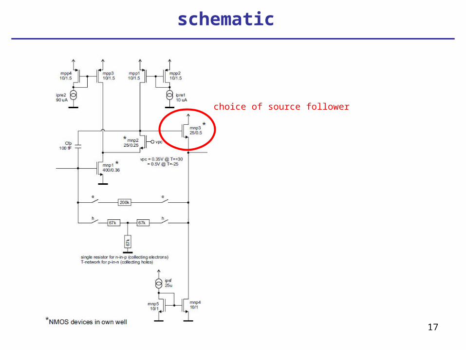
schematic
choice of source follower

18
source follower
CLOAD
NMOSsits in own (triple) well, so get gain close to 1
not a critical device – just has to drive ~ 1pF
IPSF determined by slew-ratenormal signal size ~ 4 fC produces pulse ~ 30 mV at preamp O/Prequire slew-rate ~ 10 x faster than overall pulse peaking time => 2 nsec
=> 15 V / sec
for CLOAD ~ 1pF => IPSF ~ 15 A
IPSF
NMOS device (IDS=25A)
W L gm
25 0.13 0.5925 0.26 0.6625 0.5 0.6525 1.0 0.5850 0.5 0.7115 0.5 0.6
for ~ 2 ns time constant need s.f. gm ~ 0.5 mA/V
simulations show need ~ 25 A to get this (or thereabouts)
device dimensions not critical (W.I.)
25/0.5 seems about right
(circuit has been extensively simulated around this point)
19
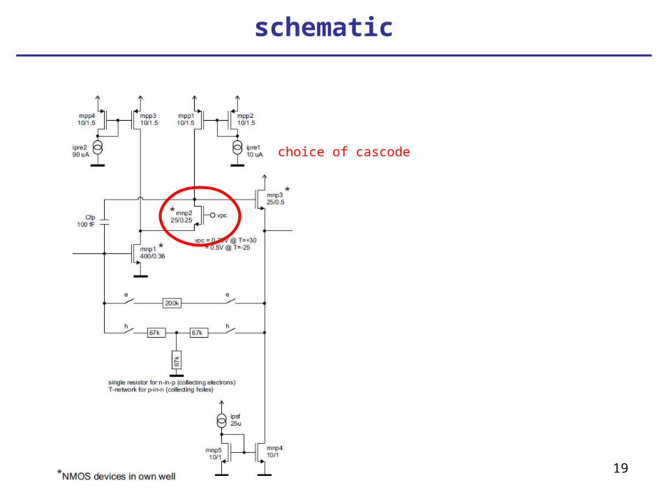
schematic
choice of cascode
20
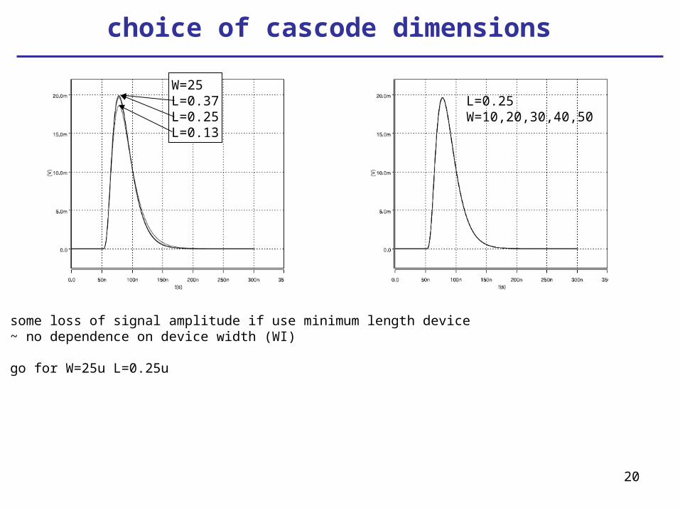
choice of cascode dimensions
W=25L=0.37L=0.25L=0.13
L=0.25W=10,20,30,40,50
some loss of signal amplitude if use minimum length device~ no dependence on device width (WI)
go for W=25u L=0.25u

21
preamp final dimensions
have justified dimensions for ~ all preamp transistors
will now proceed to simulated performance
treat electron and hole signal cases separately
but discuss adjustments required for temperaturevariation first

22
cascode bias vs temperature
inpnp1
np2
np3npc
T = -40 T = 0 T = +40
NMOS VT reduces as T increases => V across cascode gets too smallif cascode gate voltage left unchanged with temperature

23
cascode bias vs temperature
reducing cascode gate voltage (npc) withincreasing temperature solves problem
this adjustment implicit in all followingsimulations vs temperature
this is only adjustment required for whole front end circuit to allow for temperaturevariation
T = -40 T = 0 T = +40
24
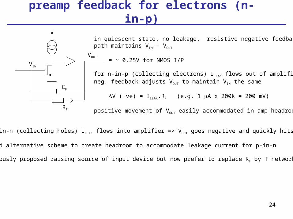
preamp feedback for electrons (n-in-p)
VIN
VOUT
in quiescent state, no leakage, resistive negative feedbackpath maintains VIN = VOUT
= ~ 0.25V for NMOS I/P
for n-in-p (collecting electrons) ILEAK flows out of amplifierneg. feedback adjusts VOUT to maintain VIN the same
V (+ve) = ILEAK.RF (e.g. 1 A x 200k = 200 mV)
positive movement of VOUT easily accommodated in amp headroom
for p-in-n (collecting holes) ILEAK flows into amplifier => VOUT goes negative and quickly hits GND
=> need alternative scheme to create headroom to accommodate leakage current for p-in-n
(previously proposed raising source of input device but now prefer to replace RF by T network)
RF
CF

25
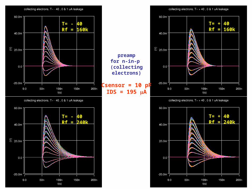
preamp performance for n-in-p (collecting electrons)
signal (at preamp O/P) from -2fC to 8fC in 1 fC stepsall process cornersT = +40 degrees
Ileak = 0
Ileak = 1uA
-ve
all pulseshapesoverlaid – DC
component removed
26
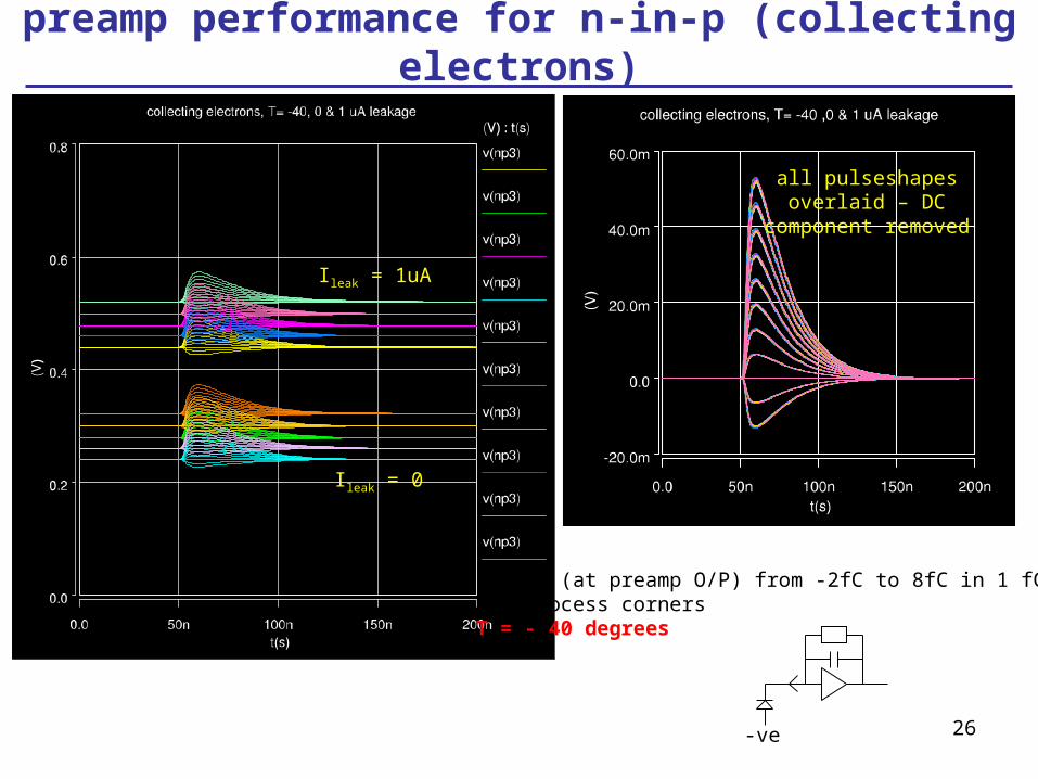
preamp performance for n-in-p (collecting electrons)
signal (at preamp O/P) from -2fC to 8fC in 1 fC stepsall process cornersT = - 40 degrees
Ileak = 0
Ileak = 1uA
-ve
all pulseshapesoverlaid – DC
component removed

27
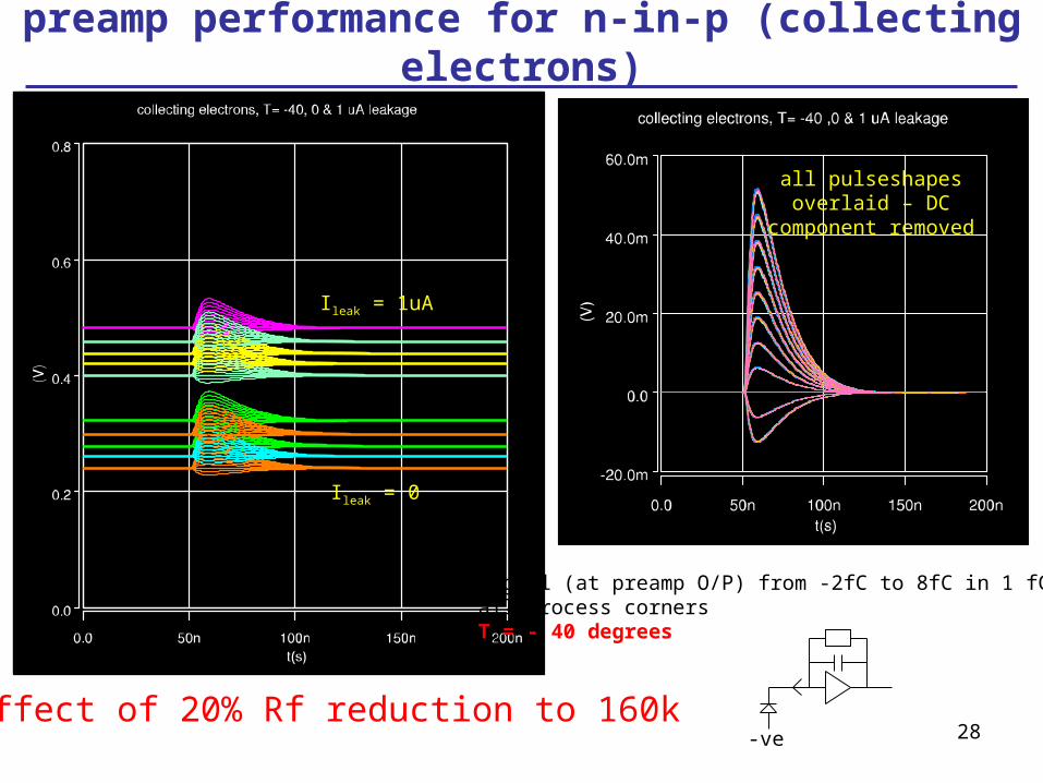
preamp performance for n-in-p (collecting electrons)
signal (at preamp O/P) from -2fC to 8fC in 1 fC stepsall process cornersT = + 40 degrees
Ileak = 0
Ileak = 1uA
-ve
all pulseshapesoverlaid – DC
component removed
Effect of 20% Rf reduction to 160k
28
preamp performance for n-in-p (collecting electrons)
signal (at preamp O/P) from -2fC to 8fC in 1 fC stepsall process cornersT = - 40 degrees
Ileak = 0
Ileak = 1uA
-ve
all pulseshapesoverlaid – DC
component removed
Effect of 20% Rf reduction to 160k
29
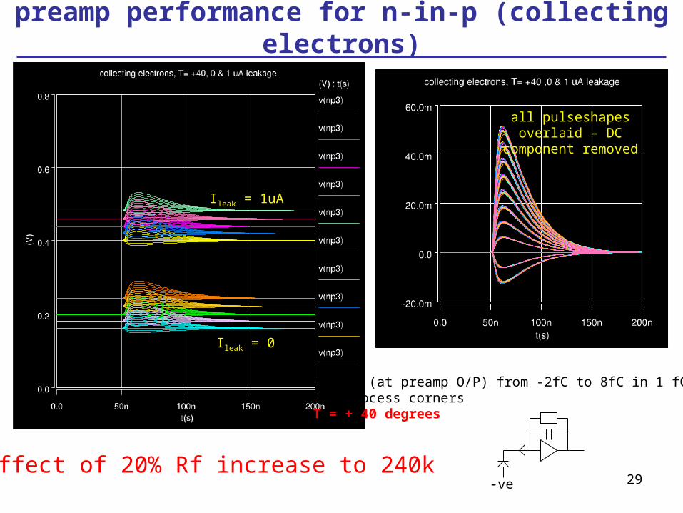
preamp performance for n-in-p (collecting electrons)
signal (at preamp O/P) from -2fC to 8fC in 1 fC stepsall process cornersT = + 40 degrees
Ileak = 0
Ileak = 1uA
-ve
all pulseshapesoverlaid – DC
component removed
Effect of 20% Rf increase to 240k

30
preamp performance for n-in-p (collecting electrons)
signal (at preamp O/P) from -2fC to 8fC in 1 fC stepsall process cornersT = - 40 degrees
Ileak = 0
Ileak = 1uA
-ve
all pulseshapesoverlaid – DC
component removed
Effect of 20% Rf increase to 240k
31
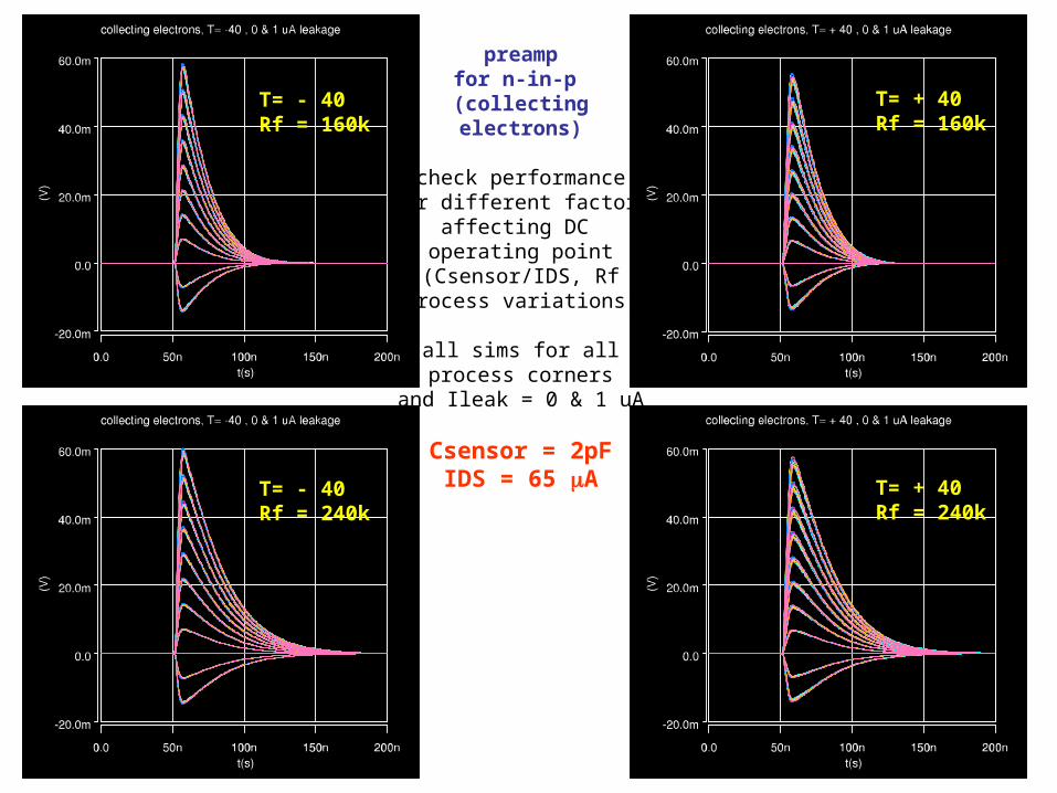
T= - 40Rf = 160k
T= - 40Rf = 240k
preampfor n-in-p (collectingelectrons)
check performancefor different factors
affecting DC operating point
(Csensor/IDS, Rfprocess variations)
all sims for allprocess corners
and Ileak = 0 & 1 uA
Csensor = 2pFIDS = 65 A
T= + 40Rf = 160k
T= + 40Rf = 240k
32
T= - 40Rf = 160k
T= - 40Rf = 240k
preampfor n-in-p (collectingelectrons)
Csensor = 10 pFIDS = 195 A
T= + 40Rf = 160k
T= + 40Rf = 240k

33
preamp performance for n-in-p (collecting electrons)
conclusions
preamp design for n-in-p looks pretty robust to extremes of:
leakage current: 0 & 1 Atemperature: -40 to +40feedback resistor variation: +/- 20%all functional process corners:
but sensor choice for outer sLHC tracker now looks likely to be p-in-n
collecting holes rather than electrons

34
preamp feedback for p-in-n
VIN
VOUT
T network of resistors in preamp feedback
in quiescent state, no leakage, resistive negative feedbackpath maintains VT = VOUT
= ~ 0.25V for NMOS I/P
=> VOUT has to shift +ve to keep VT = VIN
=> by appropriate choice of resistor values can compensate for-ve shift produced by leakage
CF
RF2RF1
RT
VT
e.g. if RF2 = 92k, RF1 = 60k, RT = 115k, then VT = VOUT/2 = 0.25V, and VOUT(quiescent) = 0.45V
If ILEAK = 1 A then VOUT shifts to 0.25V to accommodate
92k60k
115k
VIN=0.25V
ILEAK=0
2.17A
1.74AVOUT=0.45V
0.25V
92k60k
115k
VIN=0.25V
ILEAK=1A
1.65A
0.65AVOUT=0.25V
0.19V
NO LEAKAGE 1A LEAKAGE

35
preamp feedback for p-in-n
VIN
VOUT
note that VOUT(DC) depends on VIN(DC) with a gain factor 1.8
(RF2+RT) / RT
(also in single resistor n-in-p case, but there the gain factor = only 1)
So need to take care of simulating all conditions that affect DCvalue of VIN including:
Temperature and process cornersDC current in input deviceresistor process variations
CF
RF2RF1
RT
VT
92k60k
115k
the choice of actual resistor values was made (under simulation) by trying to maintain the effective noise resistance as high as possible, while ensuring satisfactory tolerance to process, temperatureand operating point variations

36
to accommodate both polarities
VIN
VOUT
need switches to select network for appropriate polarity
choice of resistor values
need CF.RF = CF.RTNETWORK
RTNETWORK = RF1 + RF2 + RF1.RF2/RT
so for RF = 200k want RNETWORK = 200k
e.g. RF1 = 60k, RF2= 92k RT = 115k
noise
T network gives increased noise
for resistor values above the effective noise resistance is 111k[60k + (92k//115k)]
=> 1.34 x noise contribution of 200k
(but still small compared with amplifier noise)
CF
RF2RF1
RT
RF
37
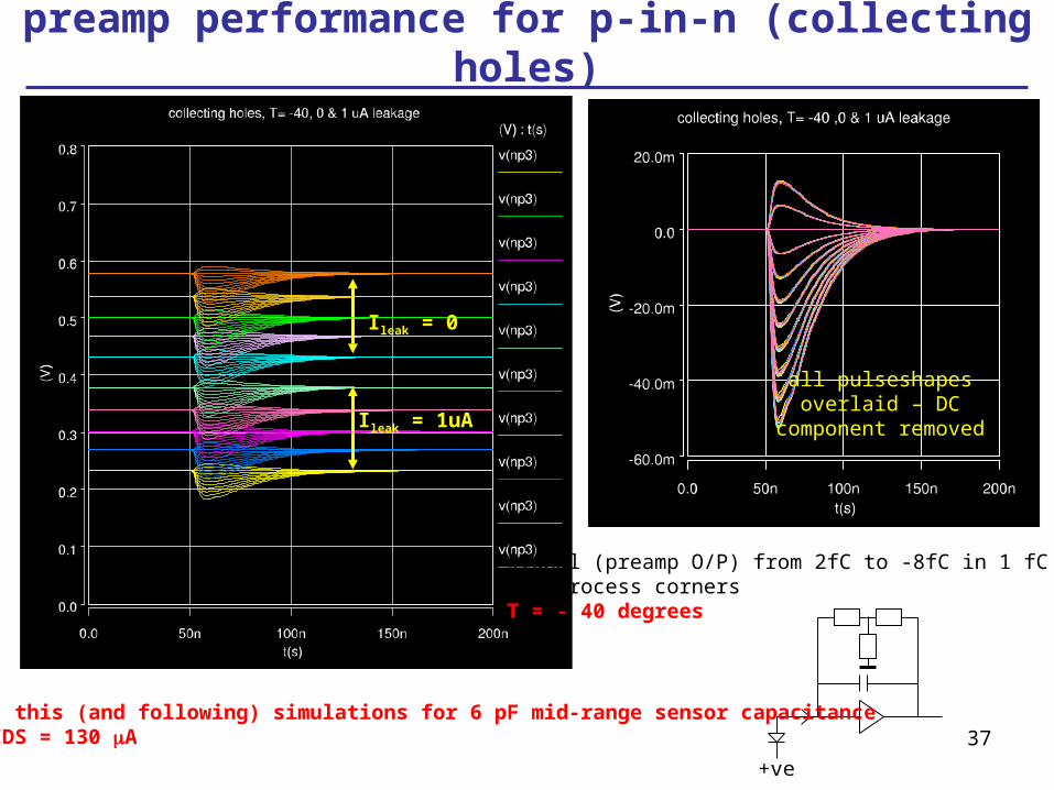
preamp performance for p-in-n (collecting holes)
signal (preamp O/P) from 2fC to -8fC in 1 fC stepsall process cornersT = - 40 degrees
Ileak = 0
Ileak = 1uA
+ve
all pulseshapesoverlaid – DC
component removed
note: this (and following) simulations for 6 pF mid-range sensor capacitanceand IDS = 130 A

38
preamp performance for p-in-n (collecting holes)
signal (preamp O/P) from 2fC to -8fC in 1 fC stepsall process cornersT = - 20 degrees
Ileak = 0
Ileak = 1uA
+ve
all pulseshapesoverlaid – DC
component removed

39
preamp performance for p-in-n (collecting holes)
signal (preamp O/P) from 2fC to -8fC in 1 fC stepsall process cornersT = 0 degrees
Ileak = 0
Ileak = 1uA
+ve
all pulseshapesoverlaid – DC
component removed

40
preamp performance for p-in-n (collecting holes)
signal (preamp O/P) from 2fC to -8fC in 1 fC stepsall process cornersT = +20 degrees
Ileak = 0
Ileak = 1uA
+ve
all pulseshapesoverlaid – DC
component removed
ILEAK = 1uA at FF corner takes Preamp O/P too close to VSS

41
preamp performance for p-in-n (collecting holes)
signal (preamp O/P) from 2fC to -8fC in 1 fC stepsall process cornersT = +20 degrees
Ileak = 0
Ileak = 1uA
+ve
all pulseshapesoverlaid – DC
component removed
Ileak = 0.85uA
tolerable ILEAK for FF corner reduced to 850nA for T=+20

42
preamp performance for p-in-n (collecting holes)
signal (preamp O/P) from 2fC to -8fC in 1 fC stepsall process cornersT = +40 degrees
Ileak = 0
Ileak = 1uA
+ve
all pulseshapesoverlaid – DC
component removed
ILEAK = 1uA at FF & FS corner takes Preamp O/P too close to VSS
FF = Fast N, Slow P

43
preamp performance for p-in-n (collecting holes)
signal (preamp O/P) from 2fC to -8fC in 1 fC stepsall process cornersT = +40 degrees
Ileak = 0
Ileak = 1uA
+ve
all pulseshapesoverlaid – DC
component removed
Ileak = 0.7uA for FF
tolerable ILEAK for FF corner reduced to 700nA for T=+20& 850nA for FS corner
Ileak = 0.85uA for FS

44
-40 -20 0 20 40
ILEAK
Temperature
1 uA
0.5 uA
0 uA
tolerated region
Slow N, Slow PSlow N, Fast PNom N, Nom PFast N, Slow PFast N, Fast P
preamp performance for p-in-n (collecting holes)
for IDS = 130 A the tolerable DC leakage current is reduced for 2 of the process cornersbut no reductions are necessary for temperatures below zero

45
preamp performance for p-in-n (collecting holes)
repeat all variety of simulations previously shown for n-in-p
use values appropriate for 2 pF (IDS=65 A) and 10 pF (IDS=195 A)(relative to nominal 130 A @ 6 pF)
and extremes of temperature (-40, +40) and Rf (-20%, +20%)
all 3 resistors in T network reduced or increased by 20% at same time
always 0 and 1 uA and all process corners
leave out the DC picture for brevity
46
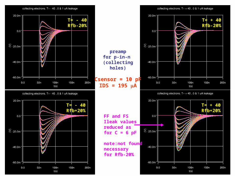
T= - 40Rfb-20%
T= - 40Rfb+20%
preampfor p-in-n (collecting
holes)
Csensor = 10 pFIDS = 195 A
T= + 40Rfb-20%
T= + 40Rfb+20%
FF and FSIleak valuesreduced asfor C = 6 pF
note:not foundnecessaryfor Rfb-20%

47
T= - 40Rfb-20%
T= - 40Rfb+20%
preampfor p-in-n (collecting
holes)
Csensor = 2 pFIDS = 65 A
T= + 40Rfb-20%
T= + 40Rfb+20%
FF and FS andTT Ileak valuesreduced
this case leasttolerant to Ileak
for FF onlyIleak valuereduced to0.8 uA

48-40 -20 0 20 40
ILEAK
Temperature
1 uA
0.5 uA
0 uA
Slow N, Slow PSlow N, Fast PNom N, Nom PFast N, Slow PFast N, Fast P
Csensor = 10 pFIDS = 195 A
-40 -20 0 20 40
ILEAK
Temperature
1 uA
0.5 uA
0 uA
Csensor = 2 pFIDS = 65 A
-40 -20 0 20 40
ILEAK
Temperature
1 uA
0.5 uA
0 uA
Rfb -20%
Rfb +20%
NORESTRICTIONS
plots show that in some cases, for higher temperatures,the tolerable DC leakage current is less than 1 A.But 1 A can be tolerated in all cases for temperaturesbelow ~ -15 degrees. Note that the coincidence of worstcase resistor tolerance, worst case process corner andworst case operating point choice is unlikely.

49
preamp performance for p-in-n (collecting holes)
conclusions
preamp design for p-in-n not quite as robust as n-in-p:
maximum spec. leakage current value cannot be tolerated under all conditionsbut can be at low operating temperature
T resistor network simple to implement (and preferable to previous off-chip resistor solution)
small extra noise contribution negligible (will show later)
50
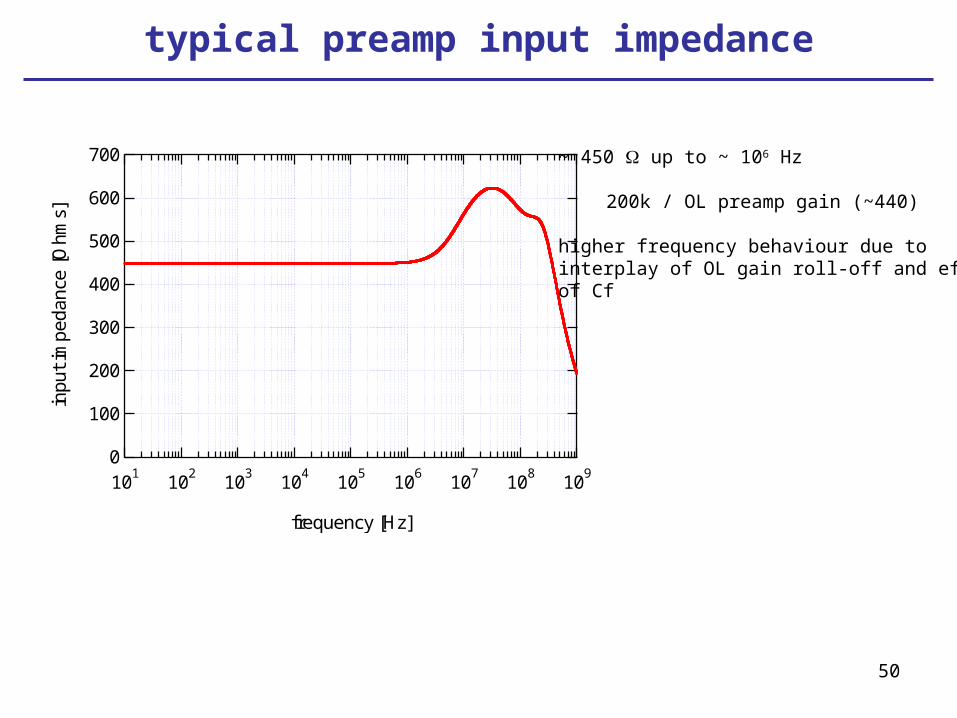
700
600
500
400
300
200
100
0
inpu
t im
peda
nce
[Ohm
s]
101
102
103
104
105
106
107
108
109
frequency [Hz]
typical preamp input impedance
~ 450 up to ~ 106 Hz
200k / OL preamp gain (~440)
higher frequency behaviour due to interplay of OL gain roll-off and effectof Cf

51
preamp conclusions
performance extensively simulated for wide rangeof operating conditions
appears robust and meets specs at target operatingconditions (with a few minor provisions for higher temps)

52
postamp
frompreamp
AC coupled to preamp
dominant pole compensated opamp
inverting configurationvoltage gain Cc / Cfpa
resistive feedback (v. high value) provided by currentmirror circuit (more details to follow)
feedback config for p-in-n (holes) shown – have toflip polarity for n-in-p (some complications here)
variable current through 16k output resistor allowsDC adjustment of level to comparator (fine tuning)
won’t discuss opamp design in detail, but concentrateon stability and resistive feedback

53
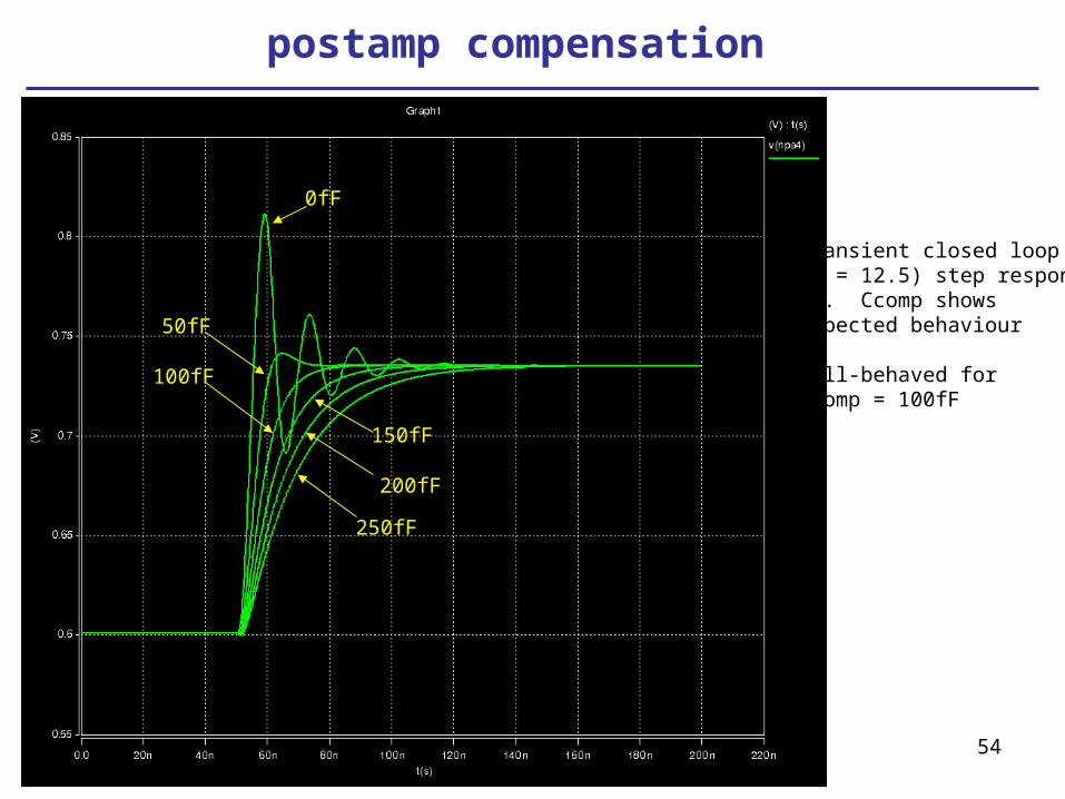
postamp compensation
0fF50fF
100fF
150fF200fF
250fF
~ 60o phase margin
OL gain and phasevs. Ccomp
want gain of ~12from postamp soneed > 60o phasemargin at ~ 20 dBfor stability
plots show stablefor gain > 20 dBwith Ccomp > 50fF
choose Ccomp = 100 fFfor greater margin
0fF
0fF
the rest
54
postamp compensation
0fF
50fF
100fF
150fF
200fF
250fF
transient closed loop(G = 12.5) step responsevs. Ccomp shows expected behaviour
well-behaved forCcomp = 100fF

55
postamp tuning
can use diff. pair tail currentto tune frequency response
10 - 30 uA gives rise timeconstant 8 – 20 us10 uA
20 uA
30 uA
8ns
20 ns

56
postamp tuning
10 uA
20 uA
30 uA
can use diff. pair tail current to achievesome pulse shapetuning
20 uA gives overall(preamp+postamp)peaking time of20 nsec
choose this fornominal value
20 ns

57
v(npa4)
postamp pulse shape (holes)
2 - 8 fC signal (holes)
6 pF preamp I/P capacitance
T = +40 & -40, all process corners
peaking time 20 nsec or less
(faster at lower temperatures)
diff pair tail current = 20 uA

58
v(npa4)
postamp pulse shape (electrons)
2 - 8 fC signal (electrons)
6 pF preamp I/P capacitance
T = +40 & -40, all process corners
peaking time 20 nsec or less
(faster at lower temperatures)
diff pair tail current = 20 uA

59
v(npa4)
postamp pulse shape (electrons)
2 - 8 fC signal (electrons)
6 pF preamp I/P capacitance
T = +40 & -40, all process corners
peaking time 20 nsec or less
(faster at lower temperatures)
diff pair tail current = 20 uA
Rfb + 20%

60
v(npa4)
postamp pulse shape (electrons)
2 - 8 fC signal (electrons)
6 pF preamp I/P capacitance
T = +40 & -40, all process corners
peaking time 20 nsec or less
(faster at lower temperatures)
diff pair tail current = 20 uA
Rfb - 20%

61
+
-
V+
30f
1p
80f
1MV+ Vpafb
electrons
+
-
V+
1p
1p
80f
1MVpafb
holes
postamp feedback
1/5
1/5 1/5
1/5
similar for both polarities, but some important differencesin how the mirroring works
Vpafb derived from current into drain-source coupled devicegives process independence Vpafb
V+
Ifpa: 0 - 25 uA
~0.6V
100/5

62
+
-
V+
V+
30f
1p
1p
80f
h
h
h
h
ee
e
1M
Vpafb
postamp feedback
can implement with switches

63
postamp feedback
VD
0.6V0.6V
ID
ID
VD
IM: 10n -> 100n, 10n steps
0.6 V
1/5 1/5
e.g. for electrons get negative going pulse at postamp output
v.high resistance for VD < 0.6
IM

64
postamp feedback – how to bias
VD
ID
1/5 1/5
Ifpa
0.6V
Ifpa
IM
IM
all process corners, T = +/- 40
1M
Vfpa
100/0.5
want IM ~ 10 to few 10’s nAbias circuit shown compensates well for temperature and processIfpa range 0 -> 25.5 uA, 8 bit precision

65
postamp feedback – for electrons
Ifpa = 0.25 uA Ifpa = 2.5 uA
Ifpa = 25 uA
Effect of Ifpa Ifpa = 0.25uA, 2.5uA and 25uA, T = - 40 & +40preamp Cin = 6 pF, all process cornerssignal injected = 2 -> 8 fC (2 fC steps)
increasing Ifpa gives noticeable overshoot
expect to operate with Ifpa small, but abilityto run with higher current (=> lower feedback R)allows to compensate for “unexpected effects”

66
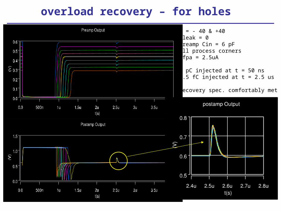
overload recovery – for electrons
T = - 40 & +40Ileak = 0preamp Cin = 6 pFall process cornersIfpa = 2.5uA
4 pC injected at t = 50 ns2.5 fC injected at t = 2.5 us
recovery spec. comfortably met

67
overload recovery – for electrons
T = - 40 & +40Ileak = 0.5uApreamp Cin = 6 pFall process cornersIfpa = 2.5uA
4 pC injected at t = 50 ns2.5 fC injected at t = 2.5 us
recovery spec. comfortably met

68
postamp feedback – for holes
Ifpa = 0.25 uA Ifpa = 2.5 uA
Ifpa = 25 uAEffect of Ifpa Ifpa = 0.25uA, 2.5uA and 25uA, T = - 40 & +40preamp Cin = 6 pF, all process cornerssignal injected = 2 -> 8 fC (2 fC steps)
similar effects to electrons case
69
overload recovery – for holes
T = - 40 & +40Ileak = 0preamp Cin = 6 pFall process cornersIfpa = 2.5uA
4 pC injected at t = 50 ns2.5 fC injected at t = 2.5 us
recovery spec. comfortably met

70
overload recovery – for holes
T = - 40 & +40Ileak = 0.5uApreamp Cin = 6 pFall process cornersIfpa = 2.5uA
4 pC injected at t = 50 ns2.5 fC injected at t = 2.5 us
recovery spec. comfortably met

71
Postamp O/P level shift
10/1 10/1
25/.5Ipaos1
10/1 10/1
Ipaos2
16k
To comp
Postamp O/P device
Lawrence’s idea for trimming comparator threshold=> don’t trim comp. threshold but trim DC level at postamp output
Ipaos1 produces DC shift across 16k (up to 10 uA -> 160 mV)
Tune Ipaos1 for desired trim value, but keep Ipaos1 + Ipaos2 constant = total required current in Postamp O/P device = 10 uA
5 bit trim gives 5 mV res’nI am thinking that now weperhaps should have more- is 6 bits possible?

72
Postamp O/P level shift
0 uA
2 uA
4 uA6 uA8 uA10 uA
Ipaos2
Ipaos1 + Ipaos2 = 10 uA
all process corners
T = +40 & -40
collecting holes

73
Postamp O/P level shift
0 uA
2 uA
4 uA
6 uA
8 uA
10 uA
Ipaos2
Ipaos1 + Ipaos2 = 10 uA
all process corners
T = +40 & -40
collecting electrons

74
comparator
VthIN
10/0.18 10/0.18
1/0.5 1/0.51/11/1
1/0.5
0.16/0.12
O/P
0.48/0.12
0.16/0.12
0.16/0.124/1
16/1 8/1
2uA
2uA
8uA
4uA
1.1 V analogue 1.2 V digital (or less)
Lawrence’s design modified
all devices now normal (low VT PMOS doesn’t seem necessary)current mirror NMOS enclosednominal supply current 14 uA (17 uW from 1.2 V)
DC coupled to postamp output – Vth global (all channels)
postamp output DC offset implements individual channel trim
last inverter implements analogue -> digital supply rail transition

75
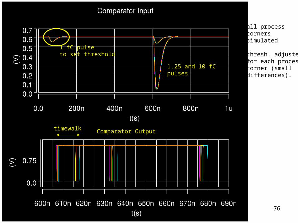
comparator timewalk specification
dependence of comparator fire time on signal sizemust be less than 1 BX(Atlas spec.)
≤ 16 ns time difference between comparator output edges for input signals of 1.25 fC and 10 fC, for a threshold setting of 1 fC
probably a good starting point
should keep under review if other threshold settings are considered(spec. defined for 300 m sensors)
76
1 fC pulseto set threshold
1.25 and 10 fCpulses
timewalk Comparator Output
all processcornerssimulated
thresh. adjustedfor each processcorner (smalldifferences).
77
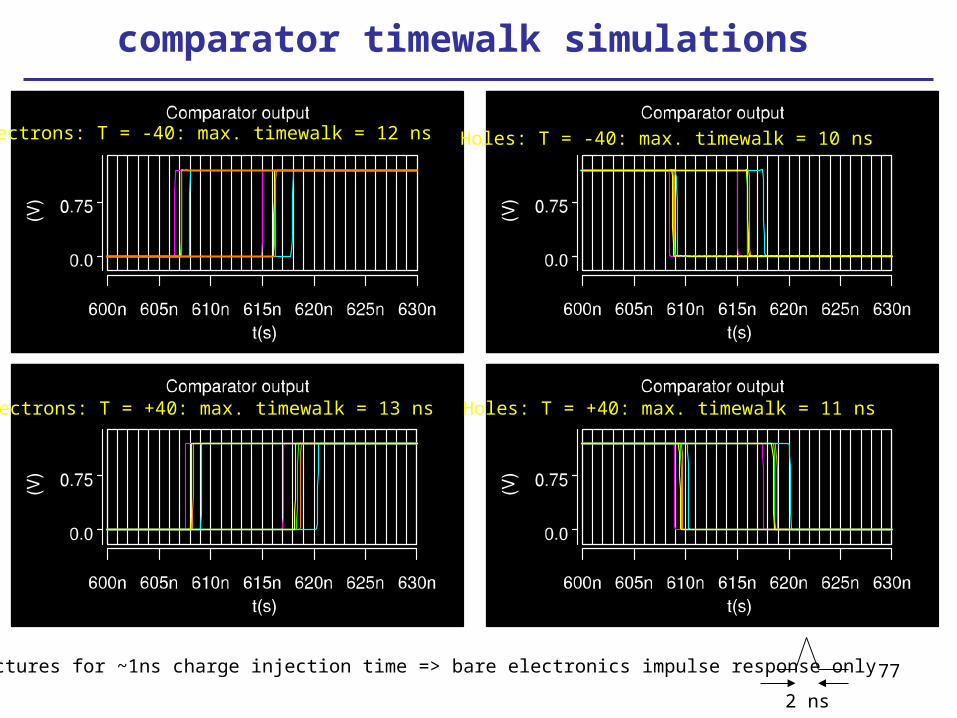
comparator timewalk simulations
Electrons: T = -40: max. timewalk = 12 ns
these pictures for ~1ns charge injection time => bare electronics impulse response only
Electrons: T = +40: max. timewalk = 13 ns Holes: T = +40: max. timewalk = 11 ns
Holes: T = -40: max. timewalk = 10 ns
2 ns

78
comparator timewalk simulations
Electrons: T = -40: max. timewalk = 14 ns
these pictures for 10ns charge injection time => spec. for sensor charge collection
Electrons: T = +40: max. timewalk = 14 ns Holes: T = +40: max. timewalk = 14 ns
Holes: T = -40: max. timewalk = 13 ns
10 ns

79
comparator conclusions
VthreshIN
10/0.18 10/0.18
1/0.5 1/0.51/11/1
1/0.5
0.16/0.12
O/P
0.48/0.12
0.16/0.12
0.16/0.124/1
16/1 8/1
2uA
2uA
8uA
4uA
1.1 V analogue 1.2 V digital (or less)
seems robust to process and temperature variations
timewalk within spec.

80
noise performance - electrons FS
SF
FFFC
SSFC
TT
T-40-200
+20+40
1200
1000
800
600
400
200
0
nois
e [r
ms
ele
ctro
ns]
1086420
Cadded [pF]
400
350
300
250
200
150
100
Po
wer [uW
]
1200
1000
800
600
400
200
0
nois
e [r
ms
ele
ctro
ns]
1086420
Cadded [pF]
400
350
300
250
200
150
100
Po
wer [uW
]
1200
1000
800
600
400
200
0
nois
e [r
ms
ele
ctro
ns]
1086420
Cadded [pF]
400
350
300
250
200
150
100
Po
wer [uW
]
1200
1000
800
600
400
200
0
nois
e [r
ms
ele
ctro
ns]
1086420
Cadded [pF]
400
350
300
250
200
150
100
Po
wer [uW
]
1200
1000
800
600
400
200
0
nois
e [r
ms
ele
ctro
ns]
1086420
Cadded [pF]
400
350
300
250
200
150
100
Po
wer [uW
]
81
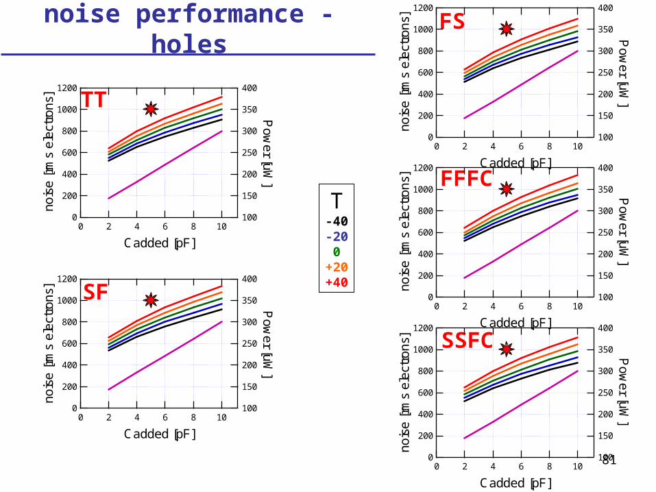
noise performance - holes FS
SF
FFFC
SSFC
TT
T-40-200
+20+40
1200
1000
800
600
400
200
0
nois
e [r
ms
ele
ctro
ns]
1086420
Cadded [pF]
400
350
300
250
200
150
100
Po
wer [uW
]
1200
1000
800
600
400
200
0
nois
e [r
ms
ele
ctro
ns]
1086420
Cadded [pF]
400
350
300
250
200
150
100
Po
wer [uW
]
1200
1000
800
600
400
200
0
nois
e [r
ms
ele
ctro
ns]
1086420
Cadded [pF]
400
350
300
250
200
150
100
Po
wer [uW
]
1200
1000
800
600
400
200
0
nois
e [r
ms
ele
ctro
ns]
1086420
Cadded [pF]
400
350
300
250
200
150
100
Po
wer [uW
]
1200
1000
800
600
400
200
0
nois
e [r
ms
ele
ctro
ns]
1086420
Cadded [pF]
400
350
300
250
200
150
100
Po
wer [uW
]
82
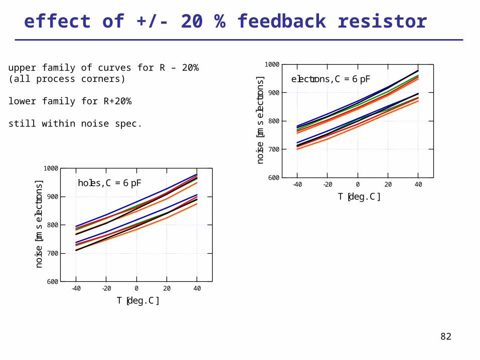
effect of +/- 20 % feedback resistor
1000
900
800
700
600
nois
e [r
ms
ele
ctro
ns]
-40 -20 0 20 40
T [deg. C]
electrons, C = 6 pF
1000
900
800
700
600
nois
e [r
ms
ele
ctro
ns]
-40 -20 0 20 40
T [deg. C]
holes, C = 6 pF
upper family of curves for R – 20%(all process corners)
lower family for R+20%
still within noise spec.

83
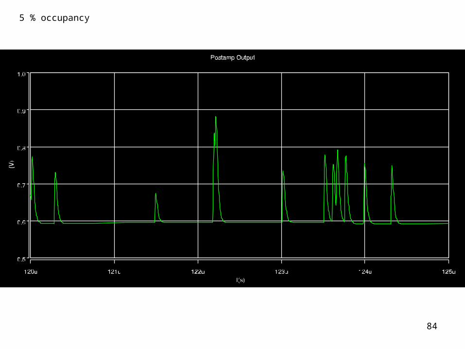
5 % occupancy
84
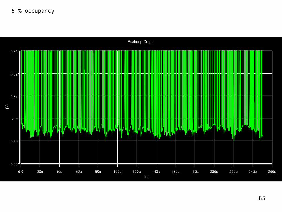
5 % occupancy
85
5 % occupancy

86
THE END

87
diff.O/P
driver
Vth(global) + V(4-bit trim)
vthDAC
vthDAC
vthDAC
pipeline readoutbuffer
logic
logic
logic
256 32
CKT1fast control
slow controlbias
test pulse
1 pulse / comp. fire
(maybe trigger logic too?)
CBC – more detailed
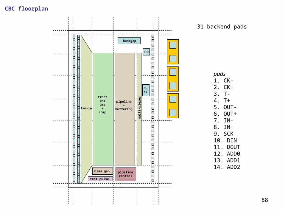
88
CBC floorplan
test pulse
fan-in
frontendamp
+comp
pipeline+
buffering
mu
lti-
ple
xer
bias gen. pipelinecontrol
bandgap
LDO
SC/2
pads1. CK-2. CK+3. T-4. T+5. OUT-6. OUT+7. IN-8. IN+9. SCK10. DIN11. DOUT12. ADD013. ADD114. ADD2
31 backend pads