z8 m icrocontroller u ser s m anual - …electronix.org.ru/datasheet/zilog/z8.pdf · z8...
TRANSCRIPT
Z8 MICROCONTROLLER
USER’S MANUAL
UM001600-Z8X0599
©1999 by ZiLOG, Inc. All rights reserved. Information in this publication concerning the devices,applications, or technology described is intended to suggest possible uses and may be superseded.ZiLOG, INC. DOES NOT ASSUME LIABILITY FOR OR PROVIDE A REPRESENTATION OFACCURACY OF THE INFORMATION, DEVICES, OR TECHNOLOGY DESCRIBED IN THISDOCUMENT. ZiLOG ALSO DOES NOT ASSUME LIABILITY FOR INTELLECTUAL PROPERTYINFRINGEMENT RELATED IN ANY MANNER TO USE OF INFORMATION, DEVICES, ORTECHNOLOGY DESCRIBED HEREIN OR OTHERWISE. Except with the express written approvalof ZiLOG, use of information, devices, or technology as critical components of life support systemsis not authorized. No licenses are conveyed, implicitly or otherwise, by this document under anyintellectual property rights.
ii UM001600-Z8X0599
U
SER
’
S
M
ANUAL
T
ABLE
OF
C
ONTENTS
Chapter Title and Subsections Page
Chapter 1. Z8 MCU Product OverviewZ8 MCU Family Overview
Key Product Line Features .................................................................................................. 1-1Product Development Support ............................................................................................. 1-3
Chapter 2. Address SpaceIntroduction ................................................................................................................................. 2-1Z8 MCU Standard Register File ..................................................................................................2-1
General-Purpose Registers ................................................................................................. 2-2RAM Protect ......................................................................................................................... 2-2Working Register Groups ..................................................................................................... 2-2Error Conditions ................................................................................................................... 2-4
Z8 Expanded Register File ....................................................................................................... 2-5Z8 Control And Peripheral Registers .......................................................................................... 2-8
Standard Z8 Registers ......................................................................................................... 2-8Expanded Z8 Registers ....................................................................................................... 2-8
Program Memory ...................................................................................................................... 2-10Z8 External Memory ................................................................................................................. 2-11
External Data Memory ....................................................................................................... 2-11Z8 STACKS .............................................................................................................................. 2-12
Chapter 3. ClockClock ........................................................................................................................................... 3-1
Frequency Control ............................................................................................................... 3-1Clock Control .............................................................................................................................. 3-1
SCLK/TCLK Divide-By-16 Select (D0) ................................................................................. 3-2External Clock Divide-By-Two (D1) ..................................................................................... 3-2
Oscillator Control ........................................................................................................................ 3-2
UM001600-Z8X0599 iii
Z8 Microcontrollers
Table of Contents
ZiLOG
Chapter Title and Subsections Page
Chapter 3. Clock (Continued)Oscillator Operation .................................................................................................................... 3-3
Layout .................................................................................................................................. 3-3Indications of an Unreliable Design ..................................................................................... 3-3Circuit Board Design Rules .................................................................................................. 3-4Crystals and Resonators ...................................................................................................... 3-5
LC Oscillator ............................................................................................................................... 3-6RC Oscillator .............................................................................................................................. 3-6
Chapter 4. ResetÑWatch-Dog TimerReset .......................................................................................................................................... 4-1Reset Pin, Internal POR Operation ............................................................................................ 4-1Watch-Dog Timer (WDT) ............................................................................................................ 4-7Power-On-Reset (POR) .............................................................................................................. 4-8
Chapter 5. I/O PortsI/O Ports ..................................................................................................................................... 5-1
Mode Registers .................................................................................................................... 5-1Input and Output Registers .................................................................................................. 5-1
Port 0 .......................................................................................................................................... 5-2General I/O Mode ................................................................................................................ 5-3Read/Write Operations ........................................................................................................ 5-4Handshake Operation .......................................................................................................... 5-4
Port 1 .......................................................................................................................................... 5-5General I/O Mode ................................................................................................................ 5-5Read/Write Operations ........................................................................................................ 5-8Handshake Operations ........................................................................................................ 5-8
PORT 2 ....................................................................................................................................... 5-9General Port I/O ................................................................................................................... 5-9Read/Write Operations ...................................................................................................... 5-12Handshake Operation ........................................................................................................ 5-12
PORT 3 ..................................................................................................................................... 5-13General Port I/O ................................................................................................................. 5-13Read/Write Operations ...................................................................................................... 5-18Special Functions ............................................................................................................... 5-18
Port Handshake ........................................................................................................................ 5-19I/O Port Reset Conditions ......................................................................................................... 5-24
Full Reset ........................................................................................................................... 5-24
Chapter 5. I/O PortsAnalog Comparators ................................................................................................................. 5-26
iv UM001600-Z8X0599
Z8 Microcontrollers
ZiLOG
Table of Contents
Chapter Title and Subsection Page
Comparator Description ..................................................................................................... 5-26Comparator Programming ................................................................................................. 5-28Comparator Operation ....................................................................................................... 5-29Interrupts ............................................................................................................................ 5-29Comparator Definitions ...................................................................................................... 5-29RUN Mode ......................................................................................................................... 5-29HALT Mode ........................................................................................................................ 5-29STOP Mode ....................................................................................................................... 5-29
Open-Drain Configuration ......................................................................................................... 5-30Low EMI Emission .................................................................................................................... 5-30Input Protection ........................................................................................................................ 5-31CMOS Z8 Auto Latches ............................................................................................................ 5-32
Chapter 6. Counter/TimersIntroduction ................................................................................................................................. 6-1Prescalers and Counter/Timers .................................................................................................. 6-2Counter/Timer Operation ............................................................................................................ 6-3
Load and Enable Count Bits ................................................................................................ 6-3Prescaler Operations ........................................................................................................... 6-4
TOUT Modes ............................................................................................................................... 6-5TIN Modes ................................................................................................................................... 6-7
External Clock Input Mode ................................................................................................... 6-8Gated Internal Clock Mode .................................................................................................. 6-9Triggered Input Mode ......................................................................................................... 6-10Retriggerable Input Mode .................................................................................................. 6-11
Cascading Counter/Timers ....................................................................................................... 6-11Reset Conditions ...................................................................................................................... 6-12
Chapter 7. InterruptsIntroduction ................................................................................................................................. 7-1Interrupt Sources ........................................................................................................................ 7-2
External Interrupt Sources ................................................................................................... 7-2Internal Interrupt Sources .................................................................................................... 7-3
Interrupt Request (IRQ) Register Logic and Timing ................................................................... 7-4Interrupt Initialization .................................................................................................................. 7-5
Interrupt Priority Register (IPR) Initialization ........................................................................ 7-5Interrupt Mask Register (IMR) Initialization .......................................................................... 7-6Interrupt Request (IRQ) Register Initialization ..................................................................... 7-7
IRQ Software Interrupt Generation ............................................................................................. 7-9
Chapter 7. Interrupts (Continued)
UM001600-Z8X0599 v
Z8 Microcontrollers
Table of Contents
ZiLOG
Chapter Title and Subsections Page
Vectored Processing .................................................................................................................. 7-9Vectored Interrupt Cycle Timing ........................................................................................ 7-11Nesting of Vectored Interrupts ........................................................................................... 7-12
Polled Processing ..................................................................................................................... 7-12Reset Conditions ...................................................................................................................... 7-12
Chapter 8. Power-Down ModesIntroduction ................................................................................................................................. 8-1HALT Mode Operation ................................................................................................................ 8-1STOP Mode Operation ............................................................................................................... 8-2STOP-Mode Recovery Register (SMR) ...................................................................................... 8-3
Chapter 9. Serial I/OUART Introduction ...................................................................................................................... 9-1UART Bit-Rate Generation ......................................................................................................... 9-2UART Receiver Operation .......................................................................................................... 9-4
Receiver Shift Register 9-4Overwrites ............................................................................................................................ 9-5Framing Errors ..................................................................................................................... 9-5Parity .................................................................................................................................... 9-5
Transmitter Operation ................................................................................................................. 9-6Overwrites ............................................................................................................................ 9-6Parity .................................................................................................................................... 9-6
UART Reset Conditions ............................................................................................................. 9-7Serial Peripheral Interface (SPI) ................................................................................................. 9-8SPI Operation ............................................................................................................................. 9-9SPI Compare .............................................................................................................................. 9-9SPI Clock .................................................................................................................................... 9-9Receive Character Available and Overrun ............................................................................... 9-11
Chapter 10. External InterfaceIntroduction ............................................................................................................................... 10-1Pin Descriptions ........................................................................................................................ 10-2
AS ...................................................................................................................................... 10-2DS ...................................................................................................................................... 10-2R/W .................................................................................................................................... 10-2DM ..................................................................................................................................... 10-2P07 - P00 ........................................................................................................................... 10-2P17 - P10 .......................................................................................................................... 10-2RESET ............................................................................................................................... 10-2XTAL1, XTAL2 ................................................................................................................... 10-2
vi UM001600-Z8X0599
Z8 Microcontrollers
ZiLOG
Table of Contents
Chapter Title and Subsection Page
External Addressing Configuration ........................................................................................... 10-3External Stacks ......................................................................................................................... 10-4Data Memory ............................................................................................................................ 10-4Bus Operation ........................................................................................................................... 10-5
Address Strobe .................................................................................................................. 10-6Data Strobe ........................................................................................................................ 10-6
Extended Bus Timing ............................................................................................................... 10-7Instruction Timing ..................................................................................................................... 10-9Z8 Reset Conditions ............................................................................................................... 10-10
Chapter 11. Addressing ModesIntroduction ............................................................................................................................... 11-1
Z8 Addressing Modes ........................................................................................................ 11-1Z8 Register Addressing (R) ...................................................................................................... 11-2Z8 Indirect Register Addressing (IR) ........................................................................................ 11-3Z8 Indexed Addressing (X) ....................................................................................................... 11-5Z8 Direct Addressing (DA) ........................................................................................................ 11-6Z8 Relative Addressing (RA) .................................................................................................... 11-7Z8 Immediate Data Addressing (IM) ......................................................................................... 11-8
Chapter 12. Instruction SetZ8 Functional Summary ........................................................................................................... 12-1Processor Flags..........................................................................................................................12-2Condition Codes.........................................................................................................................12-5Notation and Binary Coding........................................................................................................12-6Z8 Instruction Summary .............................................................................................................12-8Instruction Description and Formats.........................................................................................12-11
UM001600-Z8X0599 vii

viii UM001600-Z8X0599
U
SER
’
S
M
ANUAL
L
IST
OF
F
IGURES
Figure Title Page
Chapter 1. Z8 MCU Product OverviewZ8 MCU Block Diagram ...............................................................................................................1-2
Chap[ter 2. Address Space16-Bit Register Addressing ......................................................................................................... 2-2Accessing Individual Bits (Example) ............................................................................................2-2Working Register Addressing Examples .....................................................................................2-3Register Pointer ...........................................................................................................................2-4Expanded Register File Architecture ...........................................................................................2-5Register Pointer (FDH) Example .................................................................................................2-6Z8 Program Memory Map ..........................................................................................................2-10External Memory Map ...............................................................................................................2-11Stack Pointer .............................................................................................................................2-12Stack Operations .......................................................................................................................2-12
Chapter 3. ClockZ8 Clock Circuit ...........................................................................................................................3-1Stop-Mode Recovery Register
(Write-Only Except D7, Which is Read-Only) ...................................................................3-1External Clock Circuit ..................................................................................................................3-2Port Configuration Register (PCON) (Write-Only) .......................................................................3-2Pierce Oscillator with Internal Feedback Circuit ..........................................................................3-3Circuit Board Design Rules .........................................................................................................3-4Crystal/Ceramic Resonator Oscillator .........................................................................................3-5LC Clock ......................................................................................................................................3-5
Chapter 3. Clock (Continued)External Clock .............................................................................................................................3-5
UM001600-Z8X0599 ix
Z8 Microcontrollers
List of Figures
ZiLOG
Figure Title Page
RC Clock .....................................................................................................................................3-6
Chapter 4. ResetÑWatch-Dog TimerReset Timing ...............................................................................................................................4-2Example of External Power-On Reset Circuit ..............................................................................4-3Example of Z8 Reset with /RESET Pin, WDT, SMR, and POR ..................................................4-5Example of Z8 Reset with WDT, SMR, and POR ........................................................................4-6Example of Z8 Watch-Dog Timer Mode Register (Write-Only) ...................................................4-7Example of Z8 with Simple SMR and POR .................................................................................4-8
Chapter 5. I/O PortsI/O Ports and Mode Registers .....................................................................................................5-1 Ports 0, 1, 2 Generic Block Diagram ..........................................................................................5-2Port 0 Configuration with Open-Drain Capability, Auto Latch,
and Schmitt-Trigger ..........................................................................................................5-3Port 0 Configuration with TTL Level Shifter .......................................................5-4Port 0 I/O Operation ....................................................................................................................5-5Port 0 Handshake Operation .......................................................................................................5-5Port 1 Configuration with Open-Drain Capability, Auto Latch,
and Schmitt-Trigger ..........................................................................................................5-6Port 1 Configuration with TTL Level Shifter .................................................................................5-7Port 1 I/O Operation ....................................................................................................................5-8Handshake Operation ..................................................................................................................5-8Port 2 I/O Mode Configuration .....................................................................................................5-9Port 2 Configuration with Open-Drain Capability, Auto Latch,
and Schmitt-Trigger ..........................................................................................................5-9Port 2 Configuration with TTL Level Shifter ...............................................................................5-10Port 2 Configuration with Open-Drain Capability, Auto Latch,
Schmitt-Trigger and SPI ..................................................................................................5-11Port 2 Handshake Configuration 5 ..............................................................................................-12Port 2 Handshaking ...................................................................................................................5-12Port 3 Block Diagram .................................................................................................................5-13Port 3 Configuration with Comparator, Auto Latch, and Schmitt-Trigger ..................................5-14Port 3 Configuration with Comparator .......................................................................................5-15
Chapter 5. I/O Ports (Continued)Port 3 Configuration with SPI and Comparator Outputs
Using P34 and P35 .........................................................................................................5-16Port 3 Configuration with TTL Level Shifter and Auto Latch ......................................................5-17Port 3 Mode Register Configuration ..........................................................................................5-18Z8 Input Handshake ..................................................................................................................5-20
x UM001600-Z8X0599
Z8 Microcontrollers
ZiLOG
List of Figures
Figure Title Page
Z8 Output Handshake ...............................................................................................................5-21Output Strobed Handshake on Port 2 .......................................................................................5-23Input Strobed Handshake on Port 2 ..........................................................................................5-23Port 0/1 Reset ............................................................................................................................5-24Port 2 Reset ...............................................................................................................................5-25Port 3 Mode Reset .....................................................................................................................5-25Port 3 Input Analog Selection ....................................................................................................5-26Port 3 Comparator Output Selection .........................................................................................5-26Port Configuration of Comparator Inputs on P31, P32, and P33 ...............................................5-27Port 3 Configuration ...................................................................................................................5-28Port 2 Configuration ...................................................................................................................5-30Port Configuration Register (PCON) (Write-Only) .....................................................................5-30Diode Input Protection ...............................................................................................................5-31OTP Diode Input Protection .......................................................................................................5-31Simplified CMOS Z8 I/O Circuit .................................................................................................5-32Auto Latch Equivalent Circuit ...........................................................................5-33Effect of Pulldown Resistors on Auto Latches ...........................................................................5-33
Chapter 6. Counter/TimersCounter/Timer Block Diagram .....................................................................................................6-1Counter/Timer Register Map .......................................................................................................6-2Prescaler 0 Register ....................................................................................................................6-2Prescaler 1 Register ....................................................................................................................6-2Counter / Timer 0 and 1 Registers ..............................................................................................6-2Timer Mode Register ...................................................................................................................6-3Starting The Count ......................................................................................................................6-3Counting Modes ..........................................................................................................................6-3Timer Mode Register (TOUT Operation) .......................................................................................6-5Port 3 Mode Register (TOUT Operation) .......................................................................................6-5T0 and T1 Output Through TOUT .................................................................................................6-6
Chapter 6. Counter/Timers (Continued)Internal Clock Output Through TOUT ........................................................................................... 6-6Timer Mode Register (TIN Operation) ..........................................................................................6-7Prescaler 1 Register (TIN Operation) ...........................................................................................6-7External Clock Input Mode ..........................................................................................................6-8Gated Clock Input Mode ..............................................................................................................6-9Triggered Clock Mode ...............................................................................................................6-10Cascaded Counter/Timers .........................................................................................................6-11Counter/Timer Reset .................................................................................................................6-12Prescaler 1 Register Reset ........................................................................................................6-12
UM001600-Z8X0599 xi
Z8 Microcontrollers
List of Figures
ZiLOG
Figure Title Page
Prescaler 0 Reset ......................................................................................................................6-12Timer Mode Register Reset .......................................................................................................6-12
Chapter 7. InterruptsInterrupt Control Registers ..........................................................................................................7-1Interrupt Block Diagram ...............................................................................................................7-1Interrupt Sources IRQ0-IRQ2 Block Diagram ..............................................................................7-2Interrupt Source IRQ3 Block Diagram .........................................................................................7-3IRQ Register Logic ......................................................................................................................7-4Interrupt Request Timing .............................................................................................................7-4Interrupt Priority Register ...................................................................................7-5Interrupt Mask Register ...............................................................................................................7-6Interrupt Request Register ..........................................................................................................7-7IRQ Reset Functional Logic Diagram ..........................................................................................7-8Effects of an Interrupt on the STACK ..........................................................................................7-9Interrupt Vectoring .....................................................................................................................7-10 Z8 Interrupt Acknowledge Timing .............................................................................................7-11
Chapter 8. Power-Down ModesSTOP-Mode Recovery Register
(Write-Only Except Bit D7, Which Is Read-Only) ..............................................................8-3STOP-Mode Recovery Source ....................................................................................................8-4
Chapter 9. Serial I/OUART Block Diagram ..................................................................................................................9-1Port 3 Mode Register (P3M) and Bit-Rate Generation ................................................................9-2Bit Rate Divide Chain .........................................................................................9-2Prescaler 0 Register (PRE0) Bit-Rate Generation ......................................................................9-3Timer Mode Register (TMR) Bit Rate Generation .......................................................................9-4Receiver Timing ...........................................................................................................................9-4Receiver Data Formats ......................................................................................9-5Port 3 Mode Register (P3M) Parity ..............................................................................................9-5Transmitter Data Formats ............................................................................................................9-6SIO Register Reset ......................................................................................................................9-7P3M Register Reset ....................................................................................................................9-7SPI Control Register (SCON) ......................................................................................................9-8SPI System Configuration .........................................................................................................9-10SPI Timing .................................................................................................................................9-11SPI Logic ...................................................................................................................................9-12SPI Data In/Out Configuration ...................................................................................................9-13SPI Clock / SPI Slave Select Output Configuration ...................................................................9-14
xii UM001600-Z8X0599
Z8 Microcontrollers
ZiLOG
List of Figures
Figure Title Page
Chapter 10. External InterfaceZ8 External Interface Pins .........................................................................................................10-1External Address Configuration .................................................................................................10-3Z8 Stack Selection .....................................................................................................................10-4Port 3 Data Memory Operation ..................................................................................................10-4External Instruction Fetch or Memory Read Cycle ....................................................................10-5External Memory Write Cycle ....................................................................................................10-6Extended External Instruction Fetch or Memory Read Cycle ....................................................10-7Extended External Memory Write Cycle ....................................................................................10-8Extended Bus Timing ................................................................................................................10-8Instruction Cycle Timing (One-Byte Instructions) ......................................................................10-9Instruction Cycle Timing (Two and Three Byte Instructions) ...................................................10-10
Chapter 11. Addressing Modes8-Bit Register Addressing ..........................................................................................................11-24-Bit Register Addressing ..........................................................................................................11-24-Bit Register Addressing ..........................................................................................................11-3Indirect Register Addressing to Program or Data Memory ........................................................11-4Indexed Register Addressing ....................................................................................................11-5Direct Addressing ......................................................................................................................11-6Relative Addressing ...................................................................................................................11-7Immediate Data Addressing ......................................................................................................11-8
UM001600-Z8X0599 xiii
Z8 Microcontrollers
List of Figures
ZiLOG
Figure Title Page
xiv UM001600-Z8X0599
U
SER
’
S
M
ANUAL
L
IST
OF TABLES
Table Title Page
Chapter 1. Z8 MCU Product OverviewZiLOG General-Purpose Microcontroller Product Family ........................................................... 1-3
Chapter 2. Address SpaceZ8 Standard Register File ........................................................................................................... 2-1Working Register Groups ........................................................................................................... 2-3ERF Bank Address ..................................................................................................................... 2-6Z8 Expanded Register File Bank Layout .................................................................................... 2-7Expanded Register File Register Bank C, WR Group 0 ............................................................. 2-8Expanded Register File Bank 0, WR Group 0 ............................................................................ 2-9Expanded Register File Bank F, WR Group 0 ............................................................................ 2-9
Chapter 4. ResetÑWatch-Dog TimerSample Control and Peripheral Register Reset Values (ERF Bank 0) ....................................... 4-2Expanded Register File Bank 0 Reset Values at RESET ........................................................... 4-3Sample Expanded Register File Bank C Reset Values .............................................................. 4-4Sample Expanded Register File Bank F Reset Values .............................................................. 4-4Time-Out Period of the WDT ...................................................................................................... 4-7
Chapter 5. I/O PortsPort 3 Line Functions ................................................................................................................ 5-19
Chapter 7. InterruptsInterrupt Types, Sources, and Vectors ....................................................................................... 7-2Interrupt Priority .......................................................................................................................... 7-5Interrupt Group Priority ............................................................................................................... 7-6IRQ Register Configuration ........................................................................................................ 7-8
UM001600-Z8X0599 xv

Z8 MicrocontrollersList of Tables ZiLOG
Table Title Page
Chapter 8. Power-Down ModesSTOP-Mode Recovery Source ................................................................................................... 8-4
Chaper 9. Serial I/OUART Register Map ................................................................................................................... 9-2Bit Rates ..................................................................................................................................... 9-3SPI Pin Configuration ................................................................................................................. 9-8
xvi UM001600-Z8X0599
USER’S MANUAL
CHAPTER 1Z8 MCU PRODUCT OVERVIEW
1.1 Z8 MCU FAMILY OVERVIEW
The ZiLOG Z8 microcontroller (MCU) product line contin-ues to expand with new product introductions. ZiLOG MCUproducts are targeted for cost-sensitive, high-volume appli-cations including consumer, automotive, security, andHVAC. It includes ROM-based products geared for high-volume production (where software is stable) and one-timeprogrammable (OTP) equivalents for prototyping as wellas volume production where time to market or code flexi-
bility is critical (Table 1-1). A variety of packaging optionsare available including plastic DIP, SOIC, PLCC, and QFP.
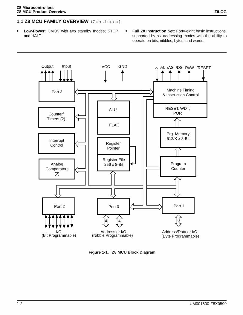
A generalized Z8 MCU® block diagram is shown in Figure1-1. The same on-chip peripherals are used across theMCU product line with the primary differences being theamount of ROM/RAM, number of I/O lines present, andpackaging/temperature ranges available. This allows codewritten for one MCU device to be easily ported to anotherfamily member.
1.1.1 Key Product Line Features¥ General-Purpose Register (GPR) File: Every RAM
register acts like an accumulator, speeding instructionexecution and maximizing coding efficiency. Workingregister groups allow fast context switching.
¥ Flexible I/O: I/O byte, nibble, and/or bit programmableas inputs or outputs. Outputs are softwareprogrammable as open-drain or push-pull on a portbasis. Inputs are Schmitt-triggered with auto latches tohold unused inputs at a known voltage state.
¥ Analog Inputs: Three input pins are softwareprogrammable as digital or analog inputs. When in theanalog mode, two comparator inputs are provided with acommon reference input. These inputs are ideal for avariety of common functions, including threshold leveldetection, analog-to-digital conversion, and short circuitdetection. Each analog input provides a uniquemaskable interrupt input.
¥ Timer/Counter(T/C): The T/C consists of aprogrammable 6-bit prescaler and 8-bit downcounter,with maskable interrupt upon end-of-count. Softwarecontrols T/C load/start/stop, countdown read (at anytime on the fly), and maskable end-of-count interrupt.Special functions available include TIN (external counterinput, external gate input, or external trigger input) andTOUT (external access to timer output or the internal
system clock.) These special functions allow accuratehardware input pulse measurement and outputwaveform generation.
¥ Interrupts: There are six vectored interrupt sources withsoftware-programmable enable and priority for each ofthe six sources.
¥ Watch-Dog Timer (WDT): An internal WDT circuit isincluded as a fail-safe mechanism so that if softwarestrays outside the bounds of normal operation, the WDTwill timeout and reset the MCU. To maximize circuitrobustness and reliability, the default WDT clock sourceis an internal RC circuit (isolated from the device clocksource).
¥ Auto Reset/Low-Voltage Protection: All familydevices have internal Power-On Reset. ROM devicesadd low-voltage protection. Low-voltage protectionensures the MCU is in a known state at all times (inactive RUN mode or RESET) without external hardware(or a device reset pin).
¥ Low-EMI Operation: Mode is programmable viasoftware or as a mask option. This new option providesfor reduced radiated emission via clock and output drivecircuit changes.
UM001600-Z8X0599 1-1
Z8 MicrocontrollersZ8 MCU Product Overview ZiLOG
1.1 Z8 MCU FAMILY OVERVIEW (Continued)
¥ Low-Power: CMOS with two standby modes; STOPand HALT.
¥ Full Z8 Instruction Set: Forty-eight basic instructions,supported by six addressing modes with the ability tooperate on bits, nibbles, bytes, and words.
Figure 1-1. Z8 MCU Block Diagram
Port 3
Counter/Timers (2)
InterruptControl
AnalogComparators
(2)
Output Input
ALU
FLAG
Register Pointer
Register File256 x 8-Bit
Machine Timing& Instruction Control
RESET, WDT, POR
Prg. Memory512/K x 8-Bit
ProgramCounter
VCC GND XTAL
Address or I/O(Nibble Programmable)
Port 2 Port 0 Port 1
/AS /DS R//W /RESET
4 4 8
Address/Data or I/O(Byte Programmable)
I/O(Bit Programmable)
1-2 UM001600-Z8X0599
Z8 MicrocontrollersZiLOG Z8 MCU Product Overview
1.1.2 Product Development SupportThe Z8 MCU product line is fully supported with a range ofcross assemblers, C compilers, ICEBOX emulators, singleand gang OTP/EPROM programmers, and softwaresimulators.
The Z86CCP01ZEM low-cost Z8 CCP™ real-time emula-tor/programmer kit was designed specifically to support allthe products outlined in Table 1-1.
The Z86CCP01ZEM kit comes with:
¥ Z8 CCP Evaluation Board
¥ Z8 CCP Power Cable
¥ ZiLOG Developer’s Studio (ZDS) CD-ROM , IncludingWindows-Based1 GUI Host Software
¥ 1999 ZiLOG Technical Library
¥ Z8 CCP User’s Manual
A Z8 CCP Emulator Accessory Kit (Z8CCP00ZAC) is alsoavailable and provides an RS-232 cable and power cablealong with the 28- and 40- pin ZIF sockets and 28- and 40-pin target connector cables required to emulate/program28/40 pin devices.
1. Windows is a trademark of the Microsoft Corporation.
Table 1-1. ZiLOG General-Purpose Microcontroller Product Family
PRODUCT ROM/RAM I/0 T/C AN INT WDT POR VBO RC SPEED PIN
IN (MHz) COUNT
Z86C03 512/60 14 1 2 6 F Y Y Y 8 18Z86E03 512/60 14 1 2 6 F Y N Y 8 18Z86C04 1K/124 14 2 2 6 F Y Y Y 8 18Z86E04 1K/124 14 2 2 6 F Y N Y 8 18Z86C06 1K/124 14 2 2 6 P Y Y Y 12 18Z86E06 1K/124 14 2 2 6 P Y N Y 12 18Z86C08 2K/124 14 2 2 6 F Y Y Y 12 18Z86E08 2K/124 14 2 2 6 F Y N Y 12 18Z86C30 4K/236 24 2 2 6 P Y Y Y 12 28Z86E30 4K/236 24 2 2 6 P Y N Y 12 28Z86C31 2K/124 24 2 2 6 P Y Y Y 8 28Z86E31 2K/124 24 2 2 6 P Y N Y 8 28Z86C40 4K/236 32 2 2 6 P Y Y Y 16 40/44Z86E40 4K/236 32 2 2 6 P Y N Y 16 40/44
Note: Z86Cxx signify ROM devices; 86xx signify EPROM devices; F = fixed; P = programmable
UM001600-Z8X0599 1-3

1-4
USER’S MANUAL
CHAPTER 2ADDRESS SPACE
2.1 INTRODUCTION
Four address spaces are available for the Z8 MCU®:
¥ The Z8 Standard Register File contains addresses forperipheral, control, all general-purpose, and all I/O portregisters. This is the default register file specification.
¥ The Z8 Expanded Register File (ERF) containsaddresses for control and data registers for additionalperipherals/features.
¥ Z8 External Program Memory contains addresses for allmemory locations having executable code and/or data.
¥ Z8 External Data Memory contains addresses for allmemory locations that hold data only, whether internal orexternal.
2.2 Z8 MCU STANDARD REGISTER FILE
The Z8 Standard Register File totals up to 256 consecutivebytes (Registers). The register file consists of 4 I/O ports(00H-03H), 236 General-Purpose Registers (04H-EFH),and 16 control registers (F0H-FFH). Table 2-1 shows thelayout of the register file, including register names, loca-tions, and identifiers.
Table 2-1. Z8 Standard Register File
Hex Register Register
Address Description Identifier
FF Stack Pointer Low Byte SPLFE Stack Pointer High Byte SPHFD Register Pointer RPFC Program Control Flags FLAGSFB Interrupt Mask Register IMRFA Interrupt Request Register IRQF9 Interrupt Priority Register IPRF8 Port 0-1 Mode Register P01MF7 Port 3 Mode Register P3MF6 Port 2 Mode Register P2MF5 T0 Prescaler PRE0F4 Timer/Counter 0 T0F3 T1 Prescaler PRE1F2 Timer/Counter 1 T1F1 Timer Mode TMR
F0 Serial I/O SIOEF R239. General-Purpose .. Registers (GPR) .. .
04 R403 Port 3 P302 Port 2 P201 Port 1 P100 Port 0 P0
Table 2-1. Z8 Standard Register File
Hex Register Register
Address Description Identifier
UM001600-Z8X0599 2-1
Z8 MicrocontrollersAddress Space ZiLOG
2.2 Z8 MCU STANDARD REGISTER FILE (Continued)
Registers can be accessed as either 8-bit or 16-bitregisters using Direct, Indirect, or Indexed Addressing. All236 general-purpose registers can be referenced ormodified by any instruction that accesses an 8-bit register,without the need for special instructions. Registersaccessed as 16 bits are treated as even-odd register pairs(there are 118 valid pairs). In this case, the data’s MostSignificant Byte (MSB) is stored in the even numberedregister, while the Least Significant Byte (LSB) goes intothe next higher odd numbered register (Figure 2-1).
By using a logical instruction and a mask, individual bitswithin registers can be accessed for bit set, bit clear, bitcomplement, or bit test operations. For example, the in-struction AND R15, MASK performs a bit clear operation.Figure 2-2 shows this example.
When instructions are executed, registers are read whendefined as sources and written when defined as destina-tions. All General-Purpose Registers function as accumu-lators, address pointers, index registers, stack areas, orscratch pad memory.
2.2.1 General-Purpose Registers General-Purpose Registers (GPR) are undefined after thedevice is powered up. The registers keep their last valueafter any reset, as long as the reset occurs in the VCC volt-age-specified operating range. It will not keep its last statefrom a VLV reset if VCC drops below 1.8v.
Note: Registers in Bank E0-EF may only be accessedthrough the working register and indirect addressingmodes. Direct access cannot be used because the 4-bitworking register address mode already uses the format [E| dst], where dst represents the working register numberfrom 0H to FH.
2.2.2 RAM ProtectThe upper portion of the register file address space 80H toEFH (excluding the control registers) may be protectedfrom reading and writing. The RAM Protect bit option ismask-programmable and is selected by the customerwhen the ROM code is submitted. After the mask option isselected, the user activates this feature from the internalROM code to turn off/on the RAM Protect by loading eithera 0 or 1 into the IMR register, bit D6. A 1 in D6 enablesRAM Protect. Only devices that use registers 80H to EFHoffer this feature.
2.2.3 Working Register GroupsZ8 instructions can access 8-bit registers and registerpairs (16-bit words) using either 4-bit or 8-bit addressfields. 8-bit address fields refer to the actual address of theregister. For example, Register 58H is accessed by callingupon its 8-bit binary equivalent, 01011000 (58H).
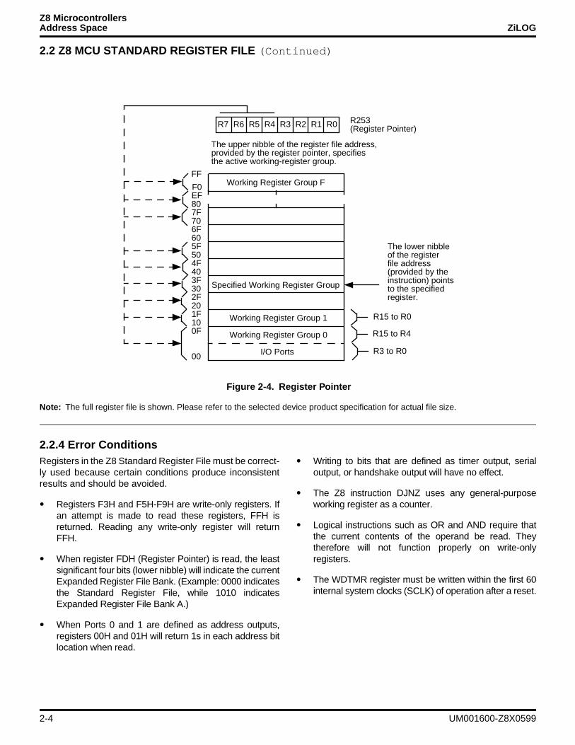
With 4-bit addressing, the register file is logically dividedinto 16 Working Register Groups of 16 registers each, asshown in Table 2-2. These 16 registers are known asWorking Registers. A Register Pointer (one of the controlregisters, FDH) contains the base address of the activeWorking Register Group. The high nibble of the RegisterPointer determines the current Working Register Group.
When accessing one of the Working Registers, the 4-bitaddress of the Working Register is combined within the up-per four bits (high nibble) of the Register Pointer, thusforming the 8-bit actual address. Figure 2-3 illustrates thisoperation. Since working registers are typically specifiedby short format instructions, there are fewer bytes of codeneeded, which reduces execution time. In addition, whenprocessing interrupts or changing tasks, the RegisterPointer speeds context switching. A special Set RegisterPointer (SRP) instruction sets the contents of the RegisterPointer.
Figure 2-1. 16-Bit Register Addressing
Figure 2-2. Accessing Individual Bits (Example)
MSB LSB
Rn Rn+1
n = Even Address
0 1 0 1 0 0 0 0
R150 1 1 1 0 0 0 0
1 1 0 1 1 1 1 1 MASK
R15
AND R15, DFH ;Clear Bit 5 of Working Register 15
2-2 UM001600-Z8X0599
Z8 MicrocontrollersZiLOG Address Space
Table 2-2. Working Register Groups
Register Pointer Working Actual
(FDH) Register Group Registers
High Nibble (HEX) (HEX)
1111(B) F F0–FF1110(B) E E0–EF1101(B) D D0–DF1100(B) C C0–CF1011(B) B B0–BF1010(B) A A0–AF1001(B) 9 90–9F1000(B) 8 80–8F0111(B) 7 70–7F0110(B) 6 60–6F0101(B) 5 50–5F0100(B) 4 40–4F0011(B) 3 30–3F0010(B) 2 20–2F0001(B) 1 10–1F0000(B) 0 00–0F
Figure 2-3. Working Register Addressing Examples
0 1 1 1 0 1 1 0
Register Pointer (FHD), Standard Register File0 1 1 1 0 0 0 0
1 1 0 1 1 1 1 1 INC R6 (Instruction, Short Format)
Actual Register Address (76H)
UM001600-Z8X0599 2-3
Z8 MicrocontrollersAddress Space ZiLOG
2.2 Z8 MCU STANDARD REGISTER FILE (Continued)
Note: The full register file is shown. Please refer to the selected device product specification for actual file size.
2.2.4 Error ConditionsRegisters in the Z8 Standard Register File must be correct-ly used because certain conditions produce inconsistentresults and should be avoided.
¥ Registers F3H and F5H-F9H are write-only registers. Ifan attempt is made to read these registers, FFH isreturned. Reading any write-only register will returnFFH.
¥ When register FDH (Register Pointer) is read, the leastsignificant four bits (lower nibble) will indicate the currentExpanded Register File Bank. (Example: 0000 indicatesthe Standard Register File, while 1010 indicatesExpanded Register File Bank A.)
¥ When Ports 0 and 1 are defined as address outputs,registers 00H and 01H will return 1s in each address bitlocation when read.
¥ Writing to bits that are defined as timer output, serialoutput, or handshake output will have no effect.
¥ The Z8 instruction DJNZ uses any general-purposeworking register as a counter.
¥ Logical instructions such as OR and AND require thatthe current contents of the operand be read. Theytherefore will not function properly on write-onlyregisters.
¥ The WDTMR register must be written within the first 60internal system clocks (SCLK) of operation after a reset.
Figure 2-4. Register Pointer
FF
F0
R7 R6 R5 R4 R3 R2 R1 R0
Specified Working Register Group
R253
I/O Ports
Working Register Group 1
Working Register Group 0
Working Register Group F
EF807F706F605F504F403F302F201F100F
00
The lower nibbleof the registerfile address(provided by theinstruction) pointsto the specifiedregister.
The upper nibble of the register file address,provided by the register pointer, specifies the active working-register group.
(Register Pointer)
R15 to R0
R15 to R4
R3 to R0
2-4 UM001600-Z8X0599
Z8 MicrocontrollersZiLOG Address Space
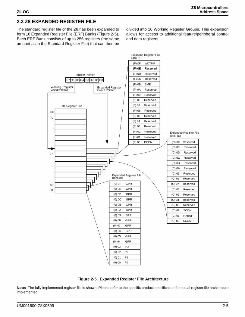
2.3 Z8 EXPANDED REGISTER FILE
The standard register file of the Z8 has been expanded toform 16 Expanded Register File (ERF) Banks (Figure 2-5).Each ERF Bank consists of up to 256 registers (the sameamount as in the Standard Register File) that can then be
divided into 16 Working Register Groups. This expansionallows for access to additional feature/peripheral controland data registers.
Note: The fully implemented register file is shown. Please refer to the specific product specification for actual register file architectureimplemented.
Figure 2-5. Expanded Register File Architecture
Z8 Register File
(F) 0F WDTMR
Expanded Register
FF
0F
7F
F0
00
Expanded Register File Bank (F)
(F) 0E Reserved
(F) 0D Reserved
(F) 0C Reserved
(F) 0B SMR
(F) 0A Reserved (F) 09 Reserved
(F) 08 Reserved
(F) 07 Reserved
(F) 06 Reserved
(F) 05 Reserved
(F) 04 Reserved
(F) 03 Reserved
(F) 0E Reserved
(F) 02 Reserved
(F) 01 Reserved
(F) 00 PCON
(0) 0F GPR
Expanded Register File Bank (0)
(0) 0E GPR
(0) 0D GPR
(0) 0C GPR
(0) 0B GPR
(0) 0A GPR
(0) 09 GPR
(0) 08 GPR
(0) 07 GPR
(0) 06 GPR
(0) 05 GPR
(0) 04 GPR
(0) 03 P3
(0) 02 P2
(0) 01 P1
(0) 00 P0
(C) 0F Reserved
Expanded Register File Bank (C)
(C) 0E Reserved
(C) 0D Reserved
(C) 0C Reserved
(C) 0B Reserved
(C) 0A Reserved
(C) 09 Reserved
(C) 08 Reserved
(C) 07 Reserved
(C) 06 Reserved
(C) 05 Reserved
(C) 04 Reserved
(C) 03 Reserved
(C) 02 SCON
(C) 01 RXBUF
(C) 00 SCOMP
D7 D6 D5 D4 D3 D2 D1 D0
Working RegisterGroup Pointer Group Pointer
Register Pointer
UM001600-Z8X0599 2-5
Z8 MicrocontrollersAddress Space ZiLOG
2.3 Z8 EXPANDED REGISTER FILE (Continued)
Currently, three out of the possible sixteen Z8 ERF Bankshave been implemented. ERF Bank 0, also known as theZ8 Standard Register File, has all 256 bytes defined (Fig-ure 2-1). Only Working Register Group 0 (register address-es 00H to 0FH) have been defined for ERF Bank C andERF Bank F (Table 2-4). All other working register groupsin ERF Banks C and F, as well as the remaining thirteenERF Banks, are not implemented. All are reserved for fu-ture use.
When an ERF Bank is selected, register addresses 00H to0FH access those sixteen ERF Bank registers – in effectreplacing the first sixteen locations of the Z8 StandardRegister File.
For example, if ERF Bank C is selected, the Z8 StandardRegisters 00H through 0FH are no longer accessible. Reg-isters 00H through 0FH are now the 16 registers from ERFBank C, Working Register Group 0. No other Z8 StandardRegisters are effected since only Working Register Group0 is implemented in ERF Bank C.
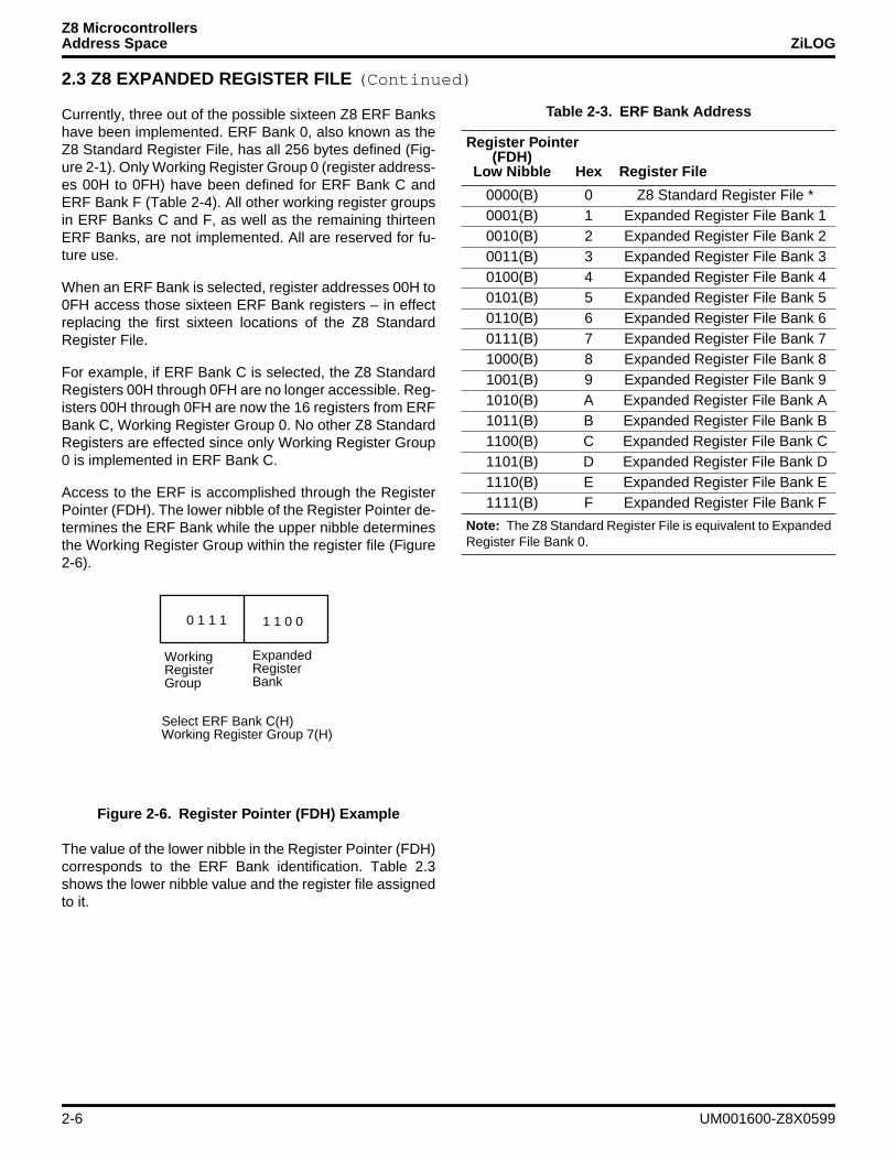
Access to the ERF is accomplished through the RegisterPointer (FDH). The lower nibble of the Register Pointer de-termines the ERF Bank while the upper nibble determinesthe Working Register Group within the register file (Figure2-6).
The value of the lower nibble in the Register Pointer (FDH)corresponds to the ERF Bank identification. Table 2.3shows the lower nibble value and the register file assignedto it.
Figure 2-6. Register Pointer (FDH) Example
0 1 1 1 1 1 0 0
Working
Select ERF Bank C(H)
RegisterGroup
ExpandedRegisterBank
Working Register Group 7(H)
Table 2-3. ERF Bank Address
Register Pointer(FDH)
Low Nibble Hex Register File
0000(B) 0 Z8 Standard Register File *0001(B) 1 Expanded Register File Bank 10010(B) 2 Expanded Register File Bank 20011(B) 3 Expanded Register File Bank 30100(B) 4 Expanded Register File Bank 40101(B) 5 Expanded Register File Bank 50110(B) 6 Expanded Register File Bank 60111(B) 7 Expanded Register File Bank 71000(B) 8 Expanded Register File Bank 81001(B) 9 Expanded Register File Bank 91010(B) A Expanded Register File Bank A1011(B) B Expanded Register File Bank B1100(B) C Expanded Register File Bank C1101(B) D Expanded Register File Bank D1110(B) E Expanded Register File Bank E1111(B) F Expanded Register File Bank F
Note: The Z8 Standard Register File is equivalent to ExpandedRegister File Bank 0.
2-6 UM001600-Z8X0599
Z8 MicrocontrollersZiLOG Address Space
The upper nibble of the register pointer selects whichgroup of 16 bytes in the Register File, out of the full 256,will be accessed as working registers.
For example:(See Figure 2-4)
Since enabling an ERF Bank (C or F) only changes regis-ter addresses 00H to 0FH, the working register pointer canbe used to access either the selected ERF Bank (Bank Cor F, Working Register Group 0) or the Z8 Standard Reg-ister File (ERF Bank 0, Working Register Groups 1 throughF).
Note: When an ERF Bank other than Bank 0 is enabled,the first 16 bytes of the Z8 Standard Register File (I/O ports0 to 3, Groups 4 to F) are no longer accessible (theselected ERF Bank, Registers 00H to 0FH are accessedinstead). It is important to re-initialize the Register Pointerto enable ERF Bank 0 when these registers are requiredfor use.
The SPI register is mapped into ERF Bank C. Access iseasily done using the following example:
Please refer to the specific product specification to deter-mine the above registers are implemented.
R253 RP = 00H ;ERF Bank 0, Working Reg. Group 0.R0 = Port 0 = 00HR1 = Port 1 = 01HR2 = Port 2 = 02HR3 = Port 3 = 03HR11 = GPR 0BHR15 = GPR 0FH
If:R253 RP = 0FH ;ERF Bank F, Working Reg. Group 0.
R0 = PCON = 00HR1 = Reserved = 01HR2 = Reserved = 02HR11 = SMR = 0BHR15 = WDTMR = 0FH
If:R253 RP = FFH ;ERF Bank F, Working Reg. Group F.
00H = PCONR0 = SI0 01H= ReservedR1 = TMR 02H= Reserved
...R2 = T1 0BH = SMR
...R15 = SPL 0FH = WDTMR
LD RP, #0CH ;Select ERF Bank C working ;register group 0 for access.
LD R2,#xx ;access SCONLD R1, #xx ;access RXBUFLD RP, #00H ;Select ERF Bank 0 so I/O ports
;are again accessible.
Table 2-4. Z8 Expanded Register File Bank Layout
ExpandedRegister File
Bank ERF
F(H) PCON, SMR, WDT,(00H, 0BH, 0FH),
Working Register Group 0 only implemented.
E(H) Not Implemented(Reserved)
D(H) Not Implemented(Reserved)
C(H) SPI Registers: SCOMP, RXBUF,
SCON (00H, 01H, 02H),Working Register Group 0
only implemented.B(H) Not Implemented
(Reserved)A(H) Not Implemented
(Reserved)9(H) Not Implemented
(Reserved)8(H) Not Implemented
(Reserved)7(H) Not Implemented
(Reserved)6(H) Not Implemented
(Reserved)5(H) Not Implemented
(Reserved)4(H) Not Implemented
(Reserved)3(H) Not Implemented
(Reserved)2(H) Not Implemented
(Reserved)1(H) Not Implemented
(Reserved)0(H) Z8 Ports 0, 1, 2, 3,
and General-Purpose Registers 04H to EFH, and control registers
F0H to FFH.
UM001600-Z8X0599 2-7
Z8 MicrocontrollersAddress Space ZiLOG
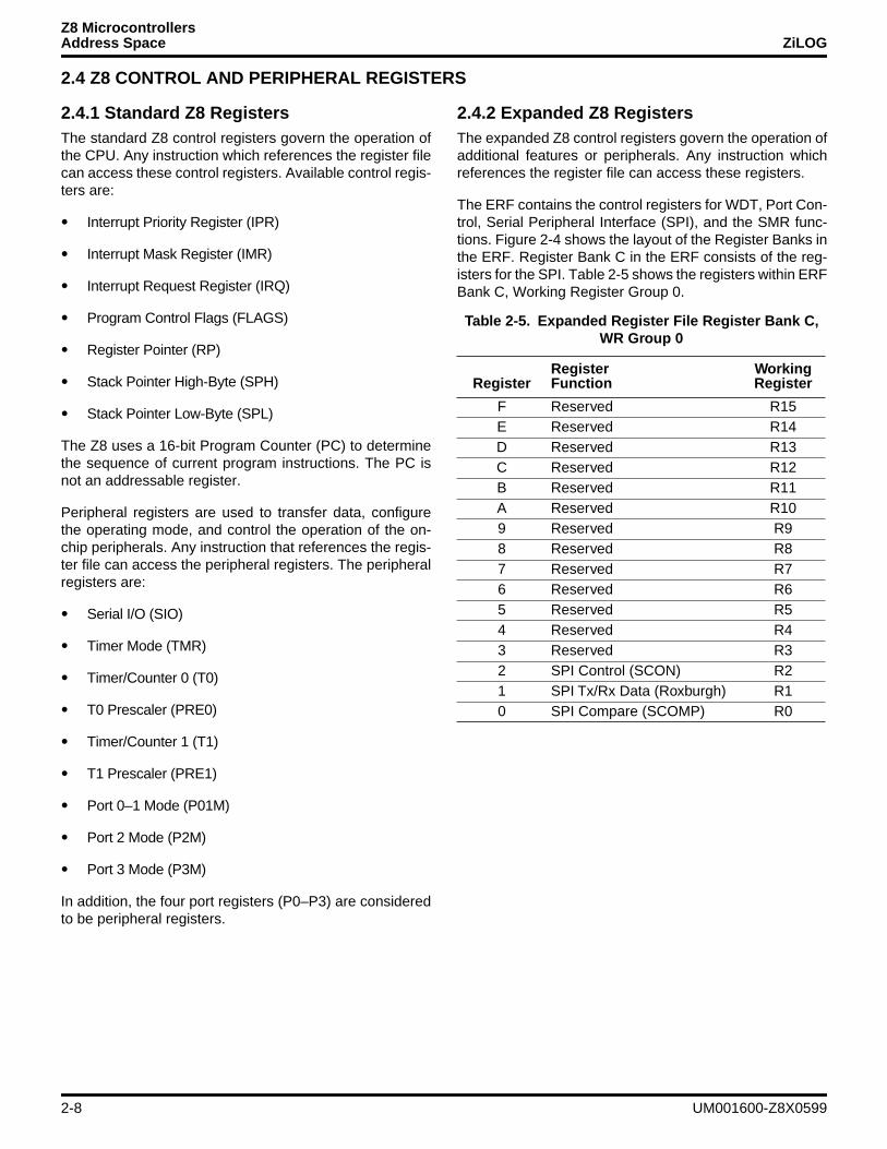
2.4 Z8 CONTROL AND PERIPHERAL REGISTERS
2.4.1 Standard Z8 RegistersThe standard Z8 control registers govern the operation ofthe CPU. Any instruction which references the register filecan access these control registers. Available control regis-ters are:
¥ Interrupt Priority Register (IPR)
¥ Interrupt Mask Register (IMR)
¥ Interrupt Request Register (IRQ)
¥ Program Control Flags (FLAGS)
¥ Register Pointer (RP)
¥ Stack Pointer High-Byte (SPH)
¥ Stack Pointer Low-Byte (SPL)
The Z8 uses a 16-bit Program Counter (PC) to determinethe sequence of current program instructions. The PC isnot an addressable register.
Peripheral registers are used to transfer data, configurethe operating mode, and control the operation of the on-chip peripherals. Any instruction that references the regis-ter file can access the peripheral registers. The peripheralregisters are:
¥ Serial I/O (SIO)
¥ Timer Mode (TMR)
¥ Timer/Counter 0 (T0)
¥ T0 Prescaler (PRE0)
¥ Timer/Counter 1 (T1)
¥ T1 Prescaler (PRE1)
¥ Port 0–1 Mode (P01M)
¥ Port 2 Mode (P2M)
¥ Port 3 Mode (P3M)
In addition, the four port registers (P0–P3) are consideredto be peripheral registers.
2.4.2 Expanded Z8 RegistersThe expanded Z8 control registers govern the operation ofadditional features or peripherals. Any instruction whichreferences the register file can access these registers.
The ERF contains the control registers for WDT, Port Con-trol, Serial Peripheral Interface (SPI), and the SMR func-tions. Figure 2-4 shows the layout of the Register Banks inthe ERF. Register Bank C in the ERF consists of the reg-isters for the SPI. Table 2-5 shows the registers within ERFBank C, Working Register Group 0.
Table 2-5. Expanded Register File Register Bank C, WR Group 0
Register WorkingRegister Function Register
F Reserved R15E Reserved R14D Reserved R13C Reserved R12B Reserved R11A Reserved R109 Reserved R98 Reserved R87 Reserved R76 Reserved R65 Reserved R54 Reserved R43 Reserved R32 SPI Control (SCON) R21 SPI Tx/Rx Data (Roxburgh) R10 SPI Compare (SCOMP) R0
2-8 UM001600-Z8X0599
Z8 MicrocontrollersZiLOG Address Space
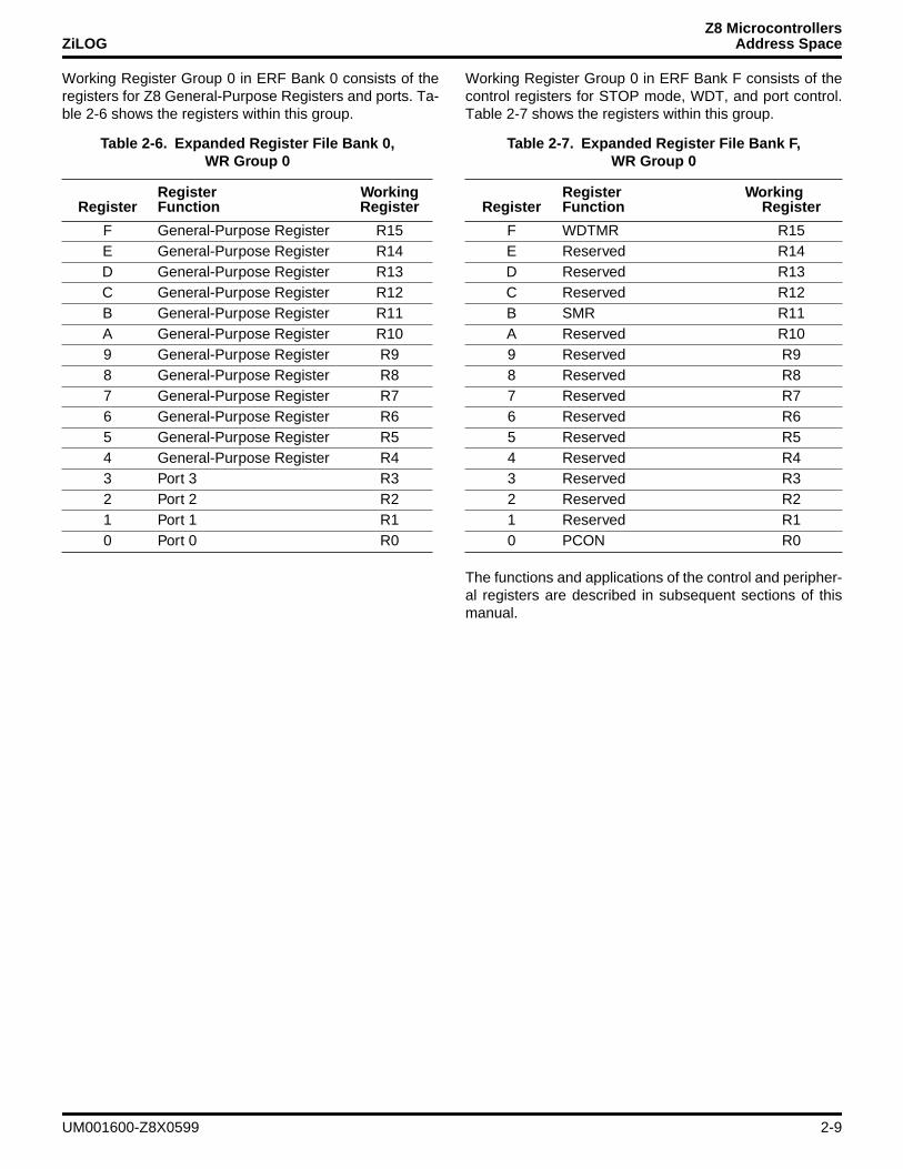
Working Register Group 0 in ERF Bank 0 consists of theregisters for Z8 General-Purpose Registers and ports. Ta-ble 2-6 shows the registers within this group.
Working Register Group 0 in ERF Bank F consists of thecontrol registers for STOP mode, WDT, and port control.Table 2-7 shows the registers within this group.
The functions and applications of the control and peripher-al registers are described in subsequent sections of thismanual.
Table 2-6. Expanded Register File Bank 0,WR Group 0
Register WorkingRegister Function Register
F General-Purpose Register R15E General-Purpose Register R14D General-Purpose Register R13C General-Purpose Register R12B General-Purpose Register R11A General-Purpose Register R109 General-Purpose Register R98 General-Purpose Register R87 General-Purpose Register R76 General-Purpose Register R65 General-Purpose Register R54 General-Purpose Register R43 Port 3 R32 Port 2 R21 Port 1 R10 Port 0 R0
Table 2-7. Expanded Register File Bank F,WR Group 0
Register WorkingRegister Function Register
F WDTMR R15E Reserved R14D Reserved R13C Reserved R12B SMR R11A Reserved R109 Reserved R98 Reserved R87 Reserved R76 Reserved R65 Reserved R54 Reserved R43 Reserved R32 Reserved R21 Reserved R10 PCON R0
UM001600-Z8X0599 2-9
Z8 MicrocontrollersAddress Space ZiLOG
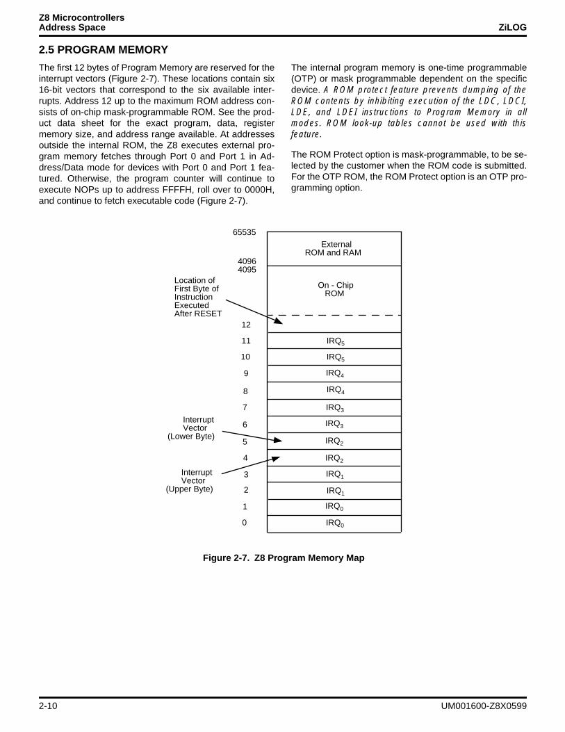
2.5 PROGRAM MEMORY
The first 12 bytes of Program Memory are reserved for theinterrupt vectors (Figure 2-7). These locations contain six16-bit vectors that correspond to the six available inter-rupts. Address 12 up to the maximum ROM address con-sists of on-chip mask-programmable ROM. See the prod-uct data sheet for the exact program, data, registermemory size, and address range available. At addressesoutside the internal ROM, the Z8 executes external pro-gram memory fetches through Port 0 and Port 1 in Ad-dress/Data mode for devices with Port 0 and Port 1 fea-tured. Otherwise, the program counter will continue toexecute NOPs up to address FFFFH, roll over to 0000H,and continue to fetch executable code (Figure 2-7).
The internal program memory is one-time programmable(OTP) or mask programmable dependent on the specificdevice. A ROM protect feature prevents dumping of theROM contents by inhibiting execution of the LDC, LDCI,LDE, and LDEI instructions to Program Memory in allmodes. ROM look-up tables cannot be used with thisfeature.
The ROM Protect option is mask-programmable, to be se-lected by the customer when the ROM code is submitted.For the OTP ROM, the ROM Protect option is an OTP pro-gramming option.
Figure 2-7. Z8 Program Memory Map
Interrupt
External
On - Chip
65535
ROM and RAM
ROM
IRQ5
4096
Interrupt
Location of
IRQ0
IRQ0
IRQ1
IRQ1
IRQ2
IRQ2
IRQ3
IRQ3
IRQ4
IRQ4
IRQ5
4095
12
1
2
3
4
5
6
7
8
9
10
11
0
First Byte ofInstructionExecutedAfter RESET
Vector(Lower Byte)
Vector(Upper Byte)
2-10 UM001600-Z8X0599
Z8 MicrocontrollersZiLOG Address Space
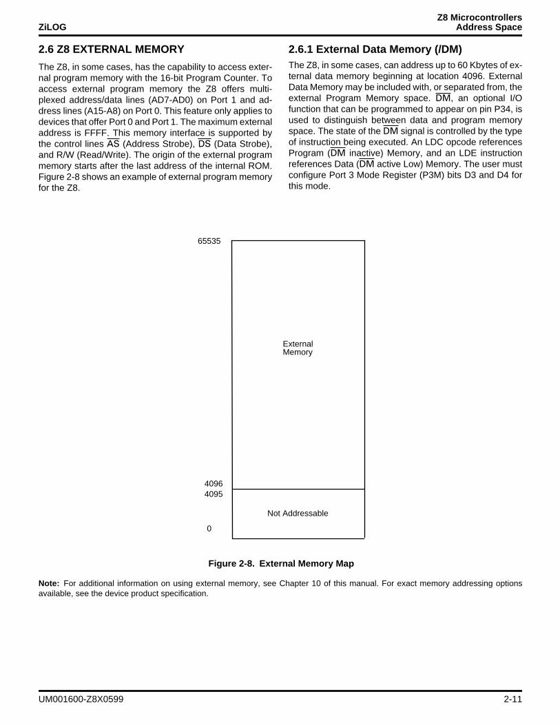
2.6 Z8 EXTERNAL MEMORY
The Z8, in some cases, has the capability to access exter-nal program memory with the 16-bit Program Counter. Toaccess external program memory the Z8 offers multi-plexed address/data lines (AD7-AD0) on Port 1 and ad-dress lines (A15-A8) on Port 0. This feature only applies todevices that offer Port 0 and Port 1. The maximum externaladdress is FFFF. This memory interface is supported bythe control lines AS (Address Strobe), DS (Data Strobe),and R/W (Read/Write). The origin of the external programmemory starts after the last address of the internal ROM.Figure 2-8 shows an example of external program memoryfor the Z8.
2.6.1 External Data Memory (/DM)The Z8, in some cases, can address up to 60 Kbytes of ex-ternal data memory beginning at location 4096. ExternalData Memory may be included with, or separated from, theexternal Program Memory space. DM, an optional I/Ofunction that can be programmed to appear on pin P34, isused to distinguish between data and program memoryspace. The state of the DM signal is controlled by the typeof instruction being executed. An LDC opcode referencesProgram (DM inactive) Memory, and an LDE instructionreferences Data (DM active Low) Memory. The user mustconfigure Port 3 Mode Register (P3M) bits D3 and D4 forthis mode.
Note: For additional information on using external memory, see Chapter 10 of this manual. For exact memory addressing optionsavailable, see the device product specification.
Figure 2-8. External Memory Map
External
65535
Memory
4096
Not Addressable
4095
0
UM001600-Z8X0599 2-11
Z8 MicrocontrollersAddress Space ZiLOG
2.7 Z8 STACKS
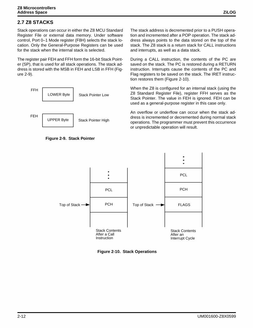
Stack operations can occur in either the Z8 MCU StandardRegister File or external data memory. Under softwarecontrol, Port 0–1 Mode register (F8H) selects the stack lo-cation. Only the General-Purpose Registers can be usedfor the stack when the internal stack is selected.
The register pair FEH and FFH form the 16-bit Stack Point-er (SP), that is used for all stack operations. The stack ad-dress is stored with the MSB in FEH and LSB in FFH (Fig-ure 2-9).
The stack address is decremented prior to a PUSH opera-tion and incremented after a POP operation. The stack ad-dress always points to the data stored on the top of thestack. The Z8 stack is a return stack for CALL instructionsand interrupts, as well as a data stack.
During a CALL instruction, the contents of the PC aresaved on the stack. The PC is restored during a RETURNinstruction. Interrupts cause the contents of the PC andFlag registers to be saved on the stack. The IRET instruc-tion restores them (Figure 2-10).
When the Z8 is configured for an internal stack (using theZ8 Standard Register File), register FFH serves as theStack Pointer. The value in FEH is ignored. FEH can beused as a general-purpose register in this case only.
An overflow or underflow can occur when the stack ad-dress is incremented or decremented during normal stackoperations. The programmer must prevent this occurrenceor unpredictable operation will result.
Figure 2-9. Stack Pointer
UPPER Byte
LOWER Byte
Stack Pointer High
FFHStack Pointer Low
FEH
Figure 2-10. Stack Operations
PCL
Top of Stack
Stack Contents
PCH
PCL
PCH
FLAGS
After anInterrupt Cycle
Stack ContentsAfter a CallInstruction
Top of Stack
2-12 UM001600-Z8X0599
USER’S MANUAL
CHAPTER 3CLOCK
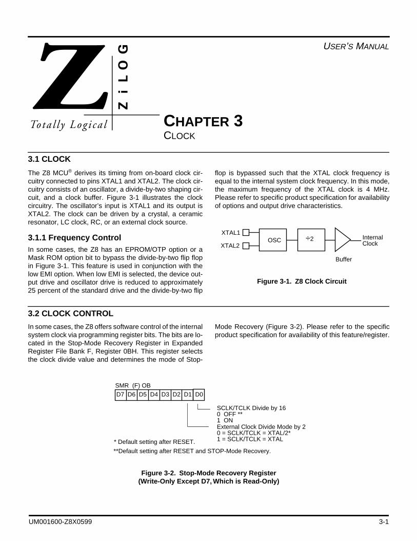
3.1 CLOCK
The Z8 MCU® derives its timing from on-board clock cir-cuitry connected to pins XTAL1 and XTAL2. The clock cir-cuitry consists of an oscillator, a divide-by-two shaping cir-cuit, and a clock buffer. Figure 3-1 illustrates the clockcircuitry. The oscillator’s input is XTAL1 and its output isXTAL2. The clock can be driven by a crystal, a ceramicresonator, LC clock, RC, or an external clock source.
3.1.1 Frequency ControlIn some cases, the Z8 has an EPROM/OTP option or aMask ROM option bit to bypass the divide-by-two flip flopin Figure 3-1. This feature is used in conjunction with thelow EMI option. When low EMI is selected, the device out-put drive and oscillator drive is reduced to approximately25 percent of the standard drive and the divide-by-two flip
flop is bypassed such that the XTAL clock frequency isequal to the internal system clock frequency. In this mode,the maximum frequency of the XTAL clock is 4 MHz.Please refer to specific product specification for availabilityof options and output drive characteristics.
3.2 CLOCK CONTROL
In some cases, the Z8 offers software control of the internalsystem clock via programming register bits. The bits are lo-cated in the Stop-Mode Recovery Register in ExpandedRegister File Bank F, Register 0BH. This register selectsthe clock divide value and determines the mode of Stop-
Mode Recovery (Figure 3-2). Please refer to the specificproduct specification for availability of this feature/register.
Figure 3-1. Z8 Clock Circuit
÷2OSCXTAL2
Internal
Buffer
XTAL1
Clock
Figure 3-2. Stop-Mode Recovery Register(Write-Only Except D7, Which is Read-Only)
D7 D6 D5 D4 D3 D2 D1 D0SMR (F) OB
SCLK/TCLK Divide by 16 0 OFF ** 1 ON External Clock Divide Mode by 2 0 = SCLK/TCLK = XTAL/2* 1 = SCLK/TCLK = XTAL * Default setting after RESET.
**Default setting after RESET and STOP-Mode Recovery.
UM001600-Z8X0599 3-1
Z8 MicrocontrollersClock ZiLOG
3.2.1 SCLK/TCLK Divide-By-16 Select (D0)This bit of the SMR controls a divide-by-16 prescalar ofSCLK/TCLK. The purpose of this control is to selectivelyreduce device power consumption during normal proces-sor execution (SCLK control) and/or HALT mode (whereTCLK sources counter/timers and interrupt logic).
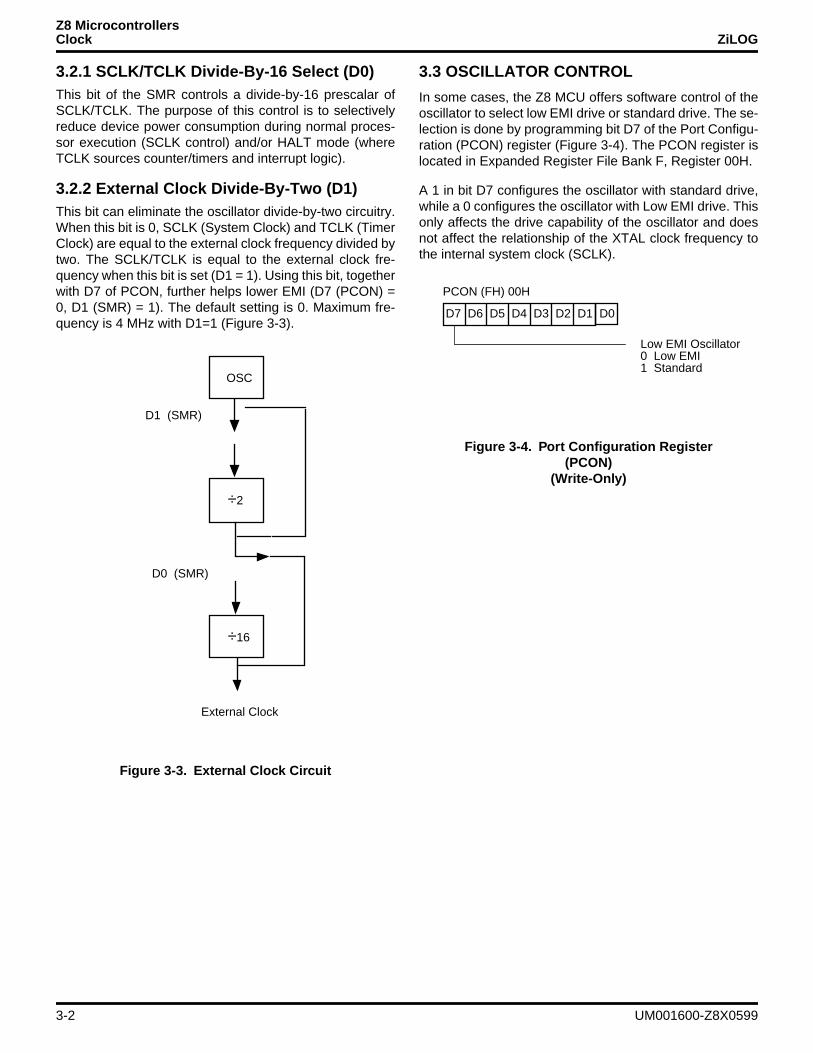
3.2.2 External Clock Divide-By-Two (D1)This bit can eliminate the oscillator divide-by-two circuitry.When this bit is 0, SCLK (System Clock) and TCLK (TimerClock) are equal to the external clock frequency divided bytwo. The SCLK/TCLK is equal to the external clock fre-quency when this bit is set (D1 = 1). Using this bit, togetherwith D7 of PCON, further helps lower EMI (D7 (PCON) =0, D1 (SMR) = 1). The default setting is 0. Maximum fre-quency is 4 MHz with D1=1 (Figure 3-3).
3.3 OSCILLATOR CONTROL
In some cases, the Z8 MCU offers software control of theoscillator to select low EMI drive or standard drive. The se-lection is done by programming bit D7 of the Port Configu-ration (PCON) register (Figure 3-4). The PCON register islocated in Expanded Register File Bank F, Register 00H.
A 1 in bit D7 configures the oscillator with standard drive,while a 0 configures the oscillator with Low EMI drive. Thisonly affects the drive capability of the oscillator and doesnot affect the relationship of the XTAL clock frequency tothe internal system clock (SCLK).
Figure 3-3. External Clock Circuit
÷2
OSC
External Clock
D1 (SMR)
÷16
D0 (SMR)
Figure 3-4. Port Configuration Register (PCON)
(Write-Only)
D7 D6 D5 D4 D3 D2 D1 D0
PCON (FH) 00H
Low EMI Oscillator 0 Low EMI 1 Standard
3-2 UM001600-Z8X0599
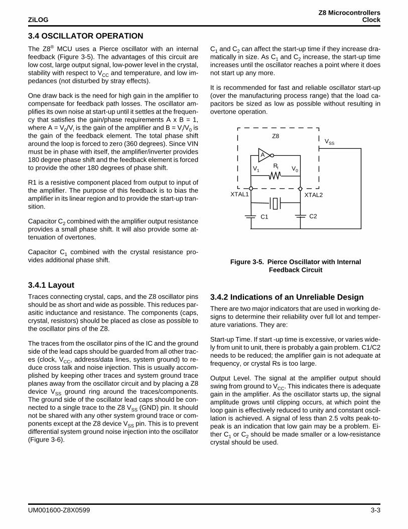
Z8 MicrocontrollersZiLOG Clock
3.4 OSCILLATOR OPERATION
The Z8® MCU uses a Pierce oscillator with an internalfeedback (Figure 3-5). The advantages of this circuit arelow cost, large output signal, low-power level in the crystal,stability with respect to VCC and temperature, and low im-pedances (not disturbed by stray effects).
One draw back is the need for high gain in the amplifier tocompensate for feedback path losses. The oscillator am-plifies its own noise at start-up until it settles at the frequen-cy that satisfies the gain/phase requirements A x B = 1,where A = V0/VI is the gain of the amplifier and B = VI/V0 isthe gain of the feedback element. The total phase shiftaround the loop is forced to zero (360 degrees). Since VINmust be in phase with itself, the amplifier/inverter provides180 degree phase shift and the feedback element is forcedto provide the other 180 degrees of phase shift.
R1 is a resistive component placed from output to input ofthe amplifier. The purpose of this feedback is to bias theamplifier in its linear region and to provide the start-up tran-sition.
Capacitor C2 combined with the amplifier output resistanceprovides a small phase shift. It will also provide some at-tenuation of overtones.
Capacitor C1 combined with the crystal resistance pro-vides additional phase shift.
C1 and C2 can affect the start-up time if they increase dra-matically in size. As C1 and C2 increase, the start-up timeincreases until the oscillator reaches a point where it doesnot start up any more.
It is recommended for fast and reliable oscillator start-up(over the manufacturing process range) that the load ca-pacitors be sized as low as possible without resulting inovertone operation.
3.4.1 LayoutTraces connecting crystal, caps, and the Z8 oscillator pinsshould be as short and wide as possible. This reduces par-asitic inductance and resistance. The components (caps,crystal, resistors) should be placed as close as possible tothe oscillator pins of the Z8.
The traces from the oscillator pins of the IC and the groundside of the lead caps should be guarded from all other trac-es (clock, VCC, address/data lines, system ground) to re-duce cross talk and noise injection. This is usually accom-plished by keeping other traces and system ground traceplanes away from the oscillator circuit and by placing a Z8device VSS ground ring around the traces/components.The ground side of the oscillator lead caps should be con-nected to a single trace to the Z8 VSS (GND) pin. It shouldnot be shared with any other system ground trace or com-ponents except at the Z8 device VSS pin. This is to preventdifferential system ground noise injection into the oscillator(Figure 3-6).
3.4.2 Indications of an Unreliable DesignThere are two major indicators that are used in working de-signs to determine their reliability over full lot and temper-ature variations. They are:
Start-up Time. If start -up time is excessive, or varies wide-ly from unit to unit, there is probably a gain problem. C1/C2needs to be reduced; the amplifier gain is not adequate atfrequency, or crystal Rs is too large.
Output Level. The signal at the amplifier output shouldswing from ground to VCC. This indicates there is adequategain in the amplifier. As the oscillator starts up, the signalamplitude grows until clipping occurs, at which point theloop gain is effectively reduced to unity and constant oscil-lation is achieved. A signal of less than 2.5 volts peak-to-peak is an indication that low gain may be a problem. Ei-ther C1 or C2 should be made smaller or a low-resistancecrystal should be used.
Figure 3-5. Pierce Oscillator with Internal Feedback Circuit
XTAL2
Z8
VSS
XTAL1
C1 C2
RI V1
A
V0
UM001600-Z8X0599 3-3
Z8 MicrocontrollersClock ZiLOG
3.4.3 Circuit Board Design RulesThe following circuit board design rules are suggested:
• To prevent induced noise the crystal and load capacitorsshould be physically located as close to the Z8® aspossible.
• Signal lines should not run parallel to the clock oscillatorinputs. In particular, the crystal input circuitry and the
internal system clock output should be separated asmuch as possible.
• VCC power lines should be separated from the clockoscillator input circuitry.
• Resistivity between XTAL1 or XTAL2 and the other pinsshould be greater than 10 Mohms.
Figure 3-6. Circuit Board Design Rules
XTAL2
VSS
XTAL1
Board Design Example
VSS
2
3
1
Layout ShouldAvoid HighLighted Areas
Signal Line
20 mmmax
Z8
Z8
Z8
C1
C2
3
2
Clock Generator Circuit
Signals A B
Signal C
(Connection to System Group Must Be Avoided)
(Parallel TracesMust Be Avoided)
(Top View)
3-4 UM001600-Z8X0599
Z8 MicrocontrollersZiLOG Clock
3.4.4 Crystals and ResonatorsCrystals and ceramic resonators (Figure 3-7) should havethe following characteristics to ensure proper oscillator op-eration:
Depending on operation frequency, the oscillator may re-quire the addition of capacitors C1 and C2 (shown in Fig-ures 3-7). The capacitance values are dependent on themanufacturer’s crystal specifications.
In most cases, the RD is 0 Ohms and RF is infinite. It is de-termined and specified by the crystal/ceramic resonatormanufacturer. The RD can be increased to decrease theamount of drive from the oscillator output to the crystal. Itcan also be used as an adjustment to avoid clipping of theoscillator signal to reduce noise. The RF can be used to im-prove the start-up of the crystal/ceramic resonator. The Z8oscillator already has an internal shunt resistor in parallelto the crystal/ceramic resonator.
It is recommended in Figures 3-7, 3-8, and 3-9 to connectthe load capacitor ground trace directly to the VSS (GND)pin of the Z8®. This ensures that no system noise is inject-ed into the Z8 clock. This trace should not be shared withany other components except at the VSS pin of the Z8.
In some cases, the Z8 XTAL1 pin also functions as one ofthe EPROM high-voltage mode programming pins or as aspecial factory test pin. In this case, applying 2 V aboveVCC on the XTAL1 pin will cause the device to enter one ofthese modes. Since this pin accepts high voltages to enterthese respective modes, the standard input protection di-ode to VCC is not on XTAL1. It is recommended that in ap-plications where the Z8 is exposed to much system noise,a diode from XTAL1 to VCC be used to prevent accidentalenabling of these modes. This diode will not affect thecrystal/ceramic resonator operation.
Please note that a parallel resonant crystal or resonatordata sheet will specify a load capacitor value that is the se-ries combination of C1 and C2, including all parasitics (PCBand holder).
Crystal Cut AT (crystal only)Mode Parallel, Fundamental ModeCrystal Capacitance <7pFLoad Capacitance 10pF < CL < 220 pF,
15 typicalResistance 100 ohms max
Figure 3-7. Crystal/Ceramic Resonator Oscillator
Figure 3-8. LC Clock
XTAL2
Z8
VSS
XTAL1
C1 C2
RF RD
XTAL2
Z8
VSS
XTAL1
C1
C2
L
Figure 3-9. External Clock
XTAL2
Z8
VSS
XTAL1
UM001600-Z8X0599 3-5
Z8 MicrocontrollersClock ZiLOG
3.5 LC OSCILLATOR
The Z8 oscillator can use a LC network to generate aXTAL clock (Figure 3-8).
The frequency stays stable over VCC and temperature. Theoscillation frequency is determined by the equation:
where L is the total inductance including parasitics and CTis the total series capacitance including the parasitics.
Simple series capacitance is calculated using the followingequation:
Sample calculation of capacitance C1 and C2 for 5.83 MHzfrequency and inductance value of 27 uH:
3.6 RC OSCILLATOR
In some cases, the Z8 has a RC oscillator option. Pleaserefer to the specific product specification for availability.The RC oscillator requires a resistor across XTAL1 andXTAL2. An additional load capacitor is required from theXTAL1 input to VSS pin (Figure 3-10).
1 Frequency = 2 π (LCT)1/2
1 = 1 + 1 CT = C1 C2
If C1 = C2
1 = 2 CT = C1
C1 = 2CT
5.83 (10^6) = 1
2π [2.7 (10-6) CT] 1/2CT = 27.6 pf
Thus C1 = 55.2 pf and C2 = 55.2 pf.
Figure 3-10. RC Clock
XTAL2
Z8
VSS
XTAL1
C1
R
3-6 UM001600-Z8X0599
USER’S MANUAL
CHAPTER 4RESET—WATCH-DOG TIMER
4.1 RESET
This section describes the Z8 MCU® reset conditions, resettiming, and register initialization procedures. Reset is gen-erated by Power-On Reset (POR), Reset Pin, Watch-DogTimer (WDT), and Stop-Mode Recovery.
A system reset overrides all other operating conditions andputs the Z8 into a known state. To initialize the chip’s inter-nal logic, the RESET input must be held Low for at least 21SCP or 5 XTAL clock cycles. The control register and portsare reset to their default conditions after a POR, a resetfrom the RESET pin, or Watch-Dog Timer timeout while in
RUN mode and HALT mode. The control registers andports are not reset to their default conditions after Stop-Mode Recovery and WDT timeout while in STOP mode.
While RESET pin is Low, AS is output at the internal clockrate, DS is forced Low, and R//W remains High. The pro-gram counter is loaded with 000CH. I/O ports and controlregisters are configured to their default reset state.
Resetting the Z8 does not effect the contents of thegeneral-purpose registers.
4.2 RESET PIN, INTERNAL POR OPERATION
In some cases, the Z8 hardware RESET pin initializes thecontrol and peripheral registers, as shown in Tables 4-1, 4-2, 4-3, and 4-4. Specific reset values are shown by 1 or 0,while bits whose states are unknown are indicated by theletter U. The Tables 4-1, 4-2, 4-3, and 4-4 show the resetconditions for the generic Z8.
Note: The register file reset state is device dependent.Please refer to the selected device product specificationsfor register availability and reset state.
UM001600-Z8X0599 4-1
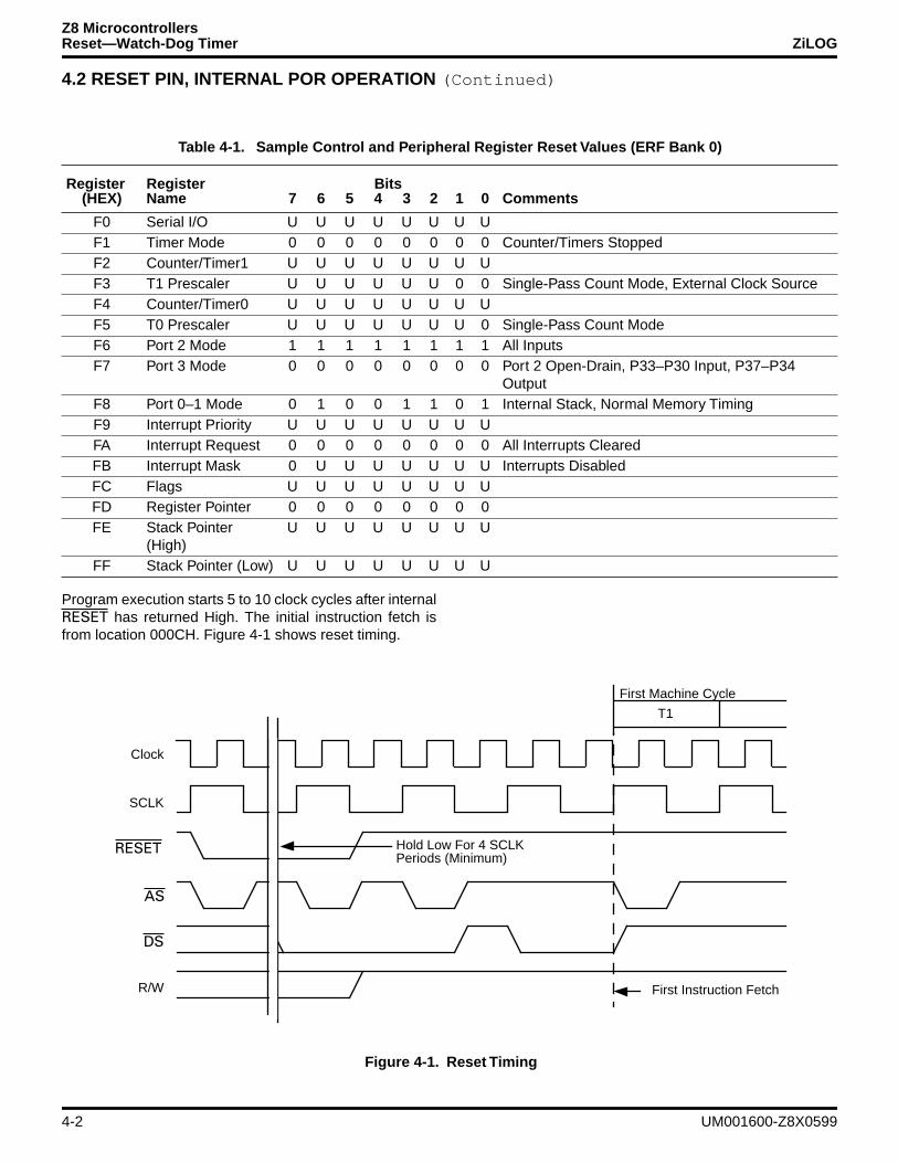
Z8 MicrocontrollersReset—Watch-Dog Timer ZiLOG
4.2 RESET PIN, INTERNAL POR OPERATION (Continued)
Program execution starts 5 to 10 clock cycles after internalRESET has returned High. The initial instruction fetch isfrom location 000CH. Figure 4-1 shows reset timing.
Table 4-1. Sample Control and Peripheral Register Reset Values (ERF Bank 0)
Register Register Bits(HEX) Name 7 6 5 4 3 2 1 0 Comments
F0 Serial I/O U U U U U U U UF1 Timer Mode 0 0 0 0 0 0 0 0 Counter/Timers StoppedF2 Counter/Timer1 U U U U U U U UF3 T1 Prescaler U U U U U U 0 0 Single-Pass Count Mode, External Clock SourceF4 Counter/Timer0 U U U U U U U UF5 T0 Prescaler U U U U U U U 0 Single-Pass Count ModeF6 Port 2 Mode 1 1 1 1 1 1 1 1 All InputsF7 Port 3 Mode 0 0 0 0 0 0 0 0 Port 2 Open-Drain, P33–P30 Input, P37–P34
OutputF8 Port 0–1 Mode 0 1 0 0 1 1 0 1 Internal Stack, Normal Memory TimingF9 Interrupt Priority U U U U U U U UFA Interrupt Request 0 0 0 0 0 0 0 0 All Interrupts Cleared FB Interrupt Mask 0 U U U U U U U Interrupts DisabledFC Flags U U U U U U U UFD Register Pointer 0 0 0 0 0 0 0 0FE Stack Pointer
(High)U U U U U U U U
FF Stack Pointer (Low) U U U U U U U U
Figure 4-1. Reset Timing
First Machine Cycle
T1
Clock
RESET
AS
DS
R/W First Instruction Fetch
Hold Low For 4 SCLKPeriods (Minimum)
SCLK
4-2 UM001600-Z8X0599
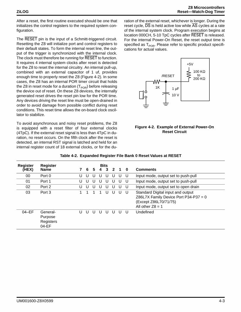
Z8 MicrocontrollersZiLOG Reset—Watch-Dog Timer
After a reset, the first routine executed should be one thatinitializes the control registers to the required system con-figuration.
The RESET pin is the input of a Schmitt-triggered circuit.Resetting the Z8 will initialize port and control registers totheir default states. To form the internal reset line, the out-put of the trigger is synchronized with the internal clock.The clock must therefore be running for RESET to function.It requires 4 internal system clocks after reset is detectedfor the Z8 to reset the internal circuitry. An internal pull-up,combined with an external capacitor of 1 uf, providesenough time to properly reset the Z8 (Figure 4-2). In somecases, the Z8 has an internal POR timer circuit that holdsthe Z8 in reset mode for a duration (TPOR) before releasingthe device out of reset. On these Z8 devices, the internallygenerated reset drives the reset pin low for the POR time.Any devices driving the reset line must be open-drained inorder to avoid damage from possible conflict during resetconditions. This reset time allows the on-board clock oscil-lator to stabilize.
To avoid asynchronous and noisy reset problems, the Z8is equipped with a reset filter of four external clocks(4TpC). If the external reset signal is less than 4TpC in du-ration, no reset occurs. On the fifth clock after the reset isdetected, an internal RST signal is latched and held for aninternal register count of 18 external clocks, or for the du-
ration of the external reset, whichever is longer. During thereset cycle, DS is held active low while AS cycles at a rateof the internal system clock. Program execution begins atlocation 000CH, 5-10 TpC cycles after RESET is released.For the internal Power-On Reset, the reset output time isspecified as TPOR. Please refer to specific product specifi-cations for actual values.
Figure 4-2. Example of External Power-On Reset Circuit
1 µF
+5V
100 KΩ/RESET
1K
to200 KΩ
10 V
Table 4-2. Expanded Register File Bank 0 Reset Values at RESET
Register Register Bits(HEX) Name 7 6 5 4 3 2 1 0 Comments
00 Port 0 U U U U U U U U Input mode, output set to push-pull01 Port 1 U U U U U U U U Input mode, output set to push-pull02 Port 2 U U U U U U U U Input mode, output set to open drain03 Port 3 1 1 1 1 U U U U Standard Digital input and output
Z86L7X Family Device Port P34-P37 = 0(Except Z86L70/71/75)All other Z8 = 1
04–EF General-PurposeRegisters04-EF
U U U U U U U U Undefined
UM001600-Z8X0599 4-3

Z8 MicrocontrollersReset—Watch-Dog Timer ZiLOG
4.2 RESET PIN, INTERNAL POR OPERATION (Continued)
Table 4-3. Sample Expanded Register File Bank C Reset Values
Register Register Bits(HEX) Name 7 6 5 4 3 2 1 0 Comments
00 SPI Compare 0 0 0 0 0 0 0 0(SCOMP)
01 Receive Buffer U U U U U U U U(RxBUF)
02 SPI Control U U U U 0 0 0 0(SCON)
Table 4-4. Sample Expanded Register File Bank F Reset Values
Register Register Bits(HEX) Name 7 6 5 4 3 2 1 0 Comments
00 Port Configuration 1 1 1 1 1 1 1 0 Comparator outputs disabled on Port 3 (PCON) Port 0 and 1 output is push-pull
Port 0, 1, 2, 3, and oscillator with standard output drive
0B STOP-Mode Recovery 0 0 1 0 0 0 0 0 Clock divide by 16 off(SMR) XTAL divide by 2
POR and / OR External ResetStop delay onStop recovery level is low, STOP flag is POR
0F Watch-Dog Timer Mode (WDTMR) U U U 0 1 1 0 1 512 TPC for WDT time out, WDT runs during
STOP
4-4 UM001600-Z8X0599
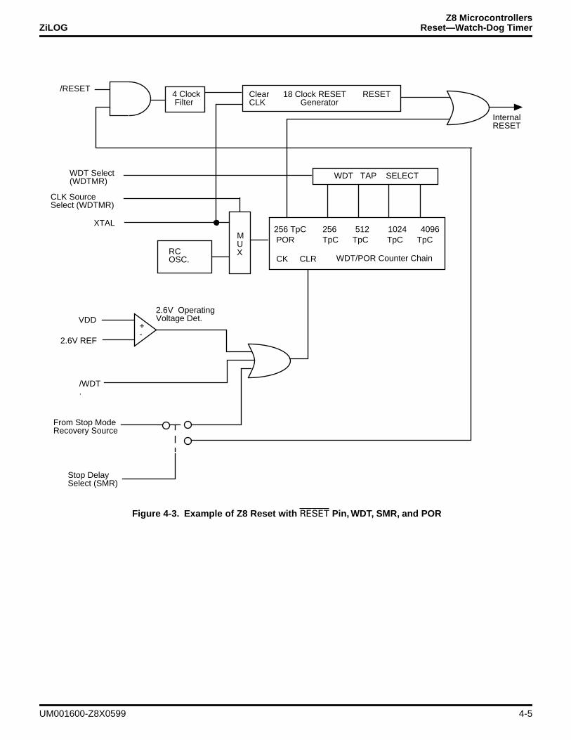
Z8 MicrocontrollersZiLOG Reset—Watch-Dog Timer
Figure 4-3. Example of Z8 Reset with RESET Pin, WDT, SMR, and POR
256 TpC 256 512 1024 4096
WDT/POR Counter Chain
POR TpC TpC TpC TpC
+-
M
WDT TAP SELECT
Clear 18 Clock RESET RESETCLK Generator
4 Clock Filter
CK CLRRCOSC.
UX
InternalRESET
2.6V OperatingVoltage Det.
/RESET
From Stop ModeRecovery Source
Stop DelaySelect (SMR)
/WDT.
VDD
XTAL
WDT Select(WDTMR)
CLK SourceSelect (WDTMR)
2.6V REF
UM001600-Z8X0599 4-5
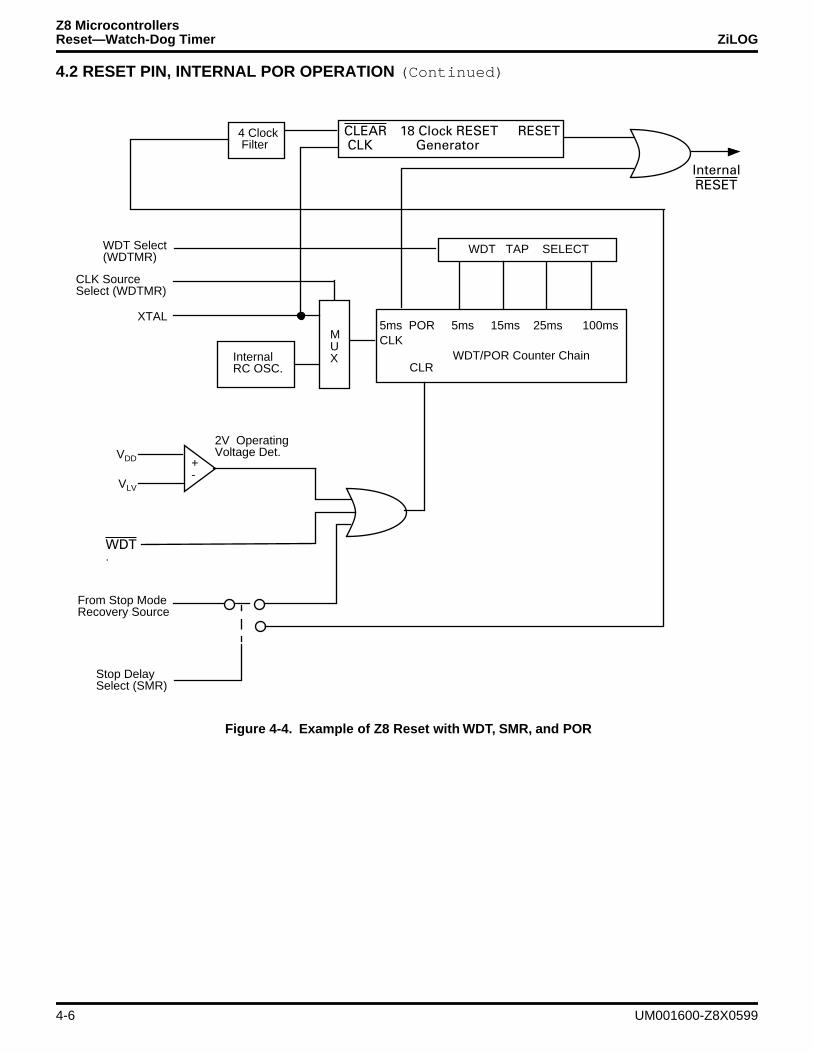
Z8 MicrocontrollersReset—Watch-Dog Timer ZiLOG
4.2 RESET PIN, INTERNAL POR OPERATION (Continued)
Figure 4-4. Example of Z8 Reset with WDT, SMR, and POR
5ms POR 5ms 15ms 25ms 100ms
WDT/POR Counter ChainCLK
+-
M
WDT TAP SELECT
4 Clock Filter
CLRInternalRC OSC.
UX
2V OperatingVoltage Det.
From Stop ModeRecovery Source
Stop DelaySelect (SMR)
WDT.
VDD
XTAL
WDT Select(WDTMR)
CLK SourceSelect (WDTMR)
VLV
InternalRESET
CLEARCLK
18 Clock RESETGenerator
RESET
4-6 UM001600-Z8X0599
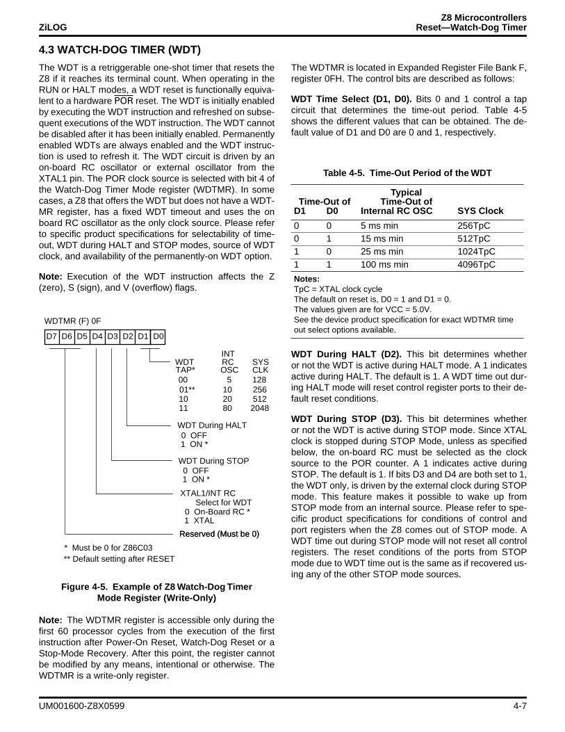
Z8 MicrocontrollersZiLOG Reset—Watch-Dog Timer
4.3 WATCH-DOG TIMER (WDT)
The WDT is a retriggerable one-shot timer that resets theZ8 if it reaches its terminal count. When operating in theRUN or HALT modes, a WDT reset is functionally equiva-lent to a hardware POR reset. The WDT is initially enabledby executing the WDT instruction and refreshed on subse-quent executions of the WDT instruction. The WDT cannotbe disabled after it has been initially enabled. Permanentlyenabled WDTs are always enabled and the WDT instruc-tion is used to refresh it. The WDT circuit is driven by anon-board RC oscillator or external oscillator from theXTAL1 pin. The POR clock source is selected with bit 4 ofthe Watch-Dog Timer Mode register (WDTMR). In somecases, a Z8 that offers the WDT but does not have a WDT-MR register, has a fixed WDT timeout and uses the onboard RC oscillator as the only clock source. Please referto specific product specifications for selectability of time-out, WDT during HALT and STOP modes, source of WDTclock, and availability of the permanently-on WDT option.
Note: Execution of the WDT instruction affects the Z(zero), S (sign), and V (overflow) flags.
Note: The WDTMR register is accessible only during thefirst 60 processor cycles from the execution of the firstinstruction after Power-On Reset, Watch-Dog Reset or aStop-Mode Recovery. After this point, the register cannotbe modified by any means, intentional or otherwise. TheWDTMR is a write-only register.
The WDTMR is located in Expanded Register File Bank F,register 0FH. The control bits are described as follows:
WDT Time Select (D1, D0). Bits 0 and 1 control a tapcircuit that determines the time-out period. Table 4-5shows the different values that can be obtained. The de-fault value of D1 and D0 are 0 and 1, respectively.
WDT During HALT (D2). This bit determines whetheror not the WDT is active during HALT mode. A 1 indicatesactive during HALT. The default is 1. A WDT time out dur-ing HALT mode will reset control register ports to their de-fault reset conditions.
WDT During STOP (D3). This bit determines whetheror not the WDT is active during STOP mode. Since XTALclock is stopped during STOP Mode, unless as specifiedbelow, the on-board RC must be selected as the clocksource to the POR counter. A 1 indicates active duringSTOP. The default is 1. If bits D3 and D4 are both set to 1,the WDT only, is driven by the external clock during STOPmode. This feature makes it possible to wake up fromSTOP mode from an internal source. Please refer to spe-cific product specifications for conditions of control andport registers when the Z8 comes out of STOP mode. AWDT time out during STOP mode will not reset all controlregisters. The reset conditions of the ports from STOPmode due to WDT time out is the same as if recovered us-ing any of the other STOP mode sources.
Figure 4-5. Example of Z8 Watch-Dog Timer Mode Register (Write-Only)
D7 D6 D5 D4 D3 D2 D1 D0
WDTMR (F) 0F
INT
00 5 128 01** 10 256
10 20 512 11 80 2048
WDT RC SYS TAP* OSC CLK
WDT During STOP 0 OFF 1 ON *
WDT During HALT 0 OFF 1 ON *
XTAL1/INT RC
0 On-Board RC * 1 XTAL
Reserved (Must be 0)
Select for WDT
* Must be 0 for Z86C03
Reserved (Must be 0)
** Default setting after RESET
Table 4-5. Time-Out Period of the WDT
TypicalTime-Out of Time-Out of
D1 D0 Internal RC OSC SYS Clock
0 0 5 ms min 256TpC0 1 15 ms min 512TpC1 0 25 ms min 1024TpC1 1 100 ms min 4096TpC
Notes: TpC = XTAL clock cycle The default on reset is, D0 = 1 and D1 = 0.The values given are for VCC = 5.0V.See the device product specification for exact WDTMR timeout select options available.
UM001600-Z8X0599 4-7
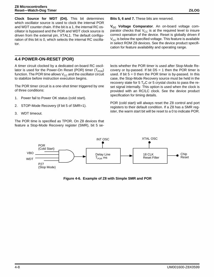
Z8 MicrocontrollersReset—Watch-Dog Timer ZiLOG
Clock Source for WDT (D4). This bit determineswhich oscillator source is used to clock the internal PORand WDT counter chain. If the bit is a 1, the internal RC os-cillator is bypassed and the POR and WDT clock source isdriven from the external pin, XTAL1. The default configu-ration of this bit is 0, which selects the internal RC oscilla-tor.
Bits 5, 6 and 7. These bits are reserved.
VCC Voltage Comparator . An on-board voltage com-parator checks that VCC is at the required level to insurecorrect operation of the device. Reset is globally driven ifVCC is below the specified voltage. This feature is availablein select ROM Z8 devices. See the device product specifi-cation for feature availability and operating range.
4.4 POWER-ON-RESET (POR)
A timer circuit clocked by a dedicated on-board RC oscil-lator is used for the Power-On Reset (POR) timer (TPOR)function. The POR time allows VCC and the oscillator circuitto stabilize before instruction execution begins.
The POR timer circuit is a one-shot timer triggered by oneof three conditions:
1. Power fail to Power OK status (cold start).
2. STOP-Mode Recovery (if bit 5 of SMR=1).
3. WDT timeout.
The POR time is specified as TPOR. On Z8 devices thatfeature a Stop-Mode Recovery register (SMR), bit 5 se-
lects whether the POR timer is used after Stop-Mode Re-covery or by-passed. If bit D5 = 1 then the POR timer isused. If bit 5 = 0 then the POR timer is by-passed. In thiscase, the Stop-Mode Recovery source must be held in therecovery state for 5 TPC or 5 crystal clocks to pass the re-set signal internally. This option is used when the clock isprovided with an RC/LC clock. See the device productspecification for timing details.
POR (cold start) will always reset the Z8 control and portregisters to their default condition. If a Z8 has a SMR reg-ister, the warm start bit will be reset to a 0 to indicate POR.
Figure 4-6. Example of Z8 with Simple SMR and POR
INT OSC
Chip
POR
Reset
P27(Stop Mode)
(Cold Start)VBO
WDTDelay LineTPOR ms
18 CLKReset Filter
XTAL OSC
4-8 UM001600-Z8X0599
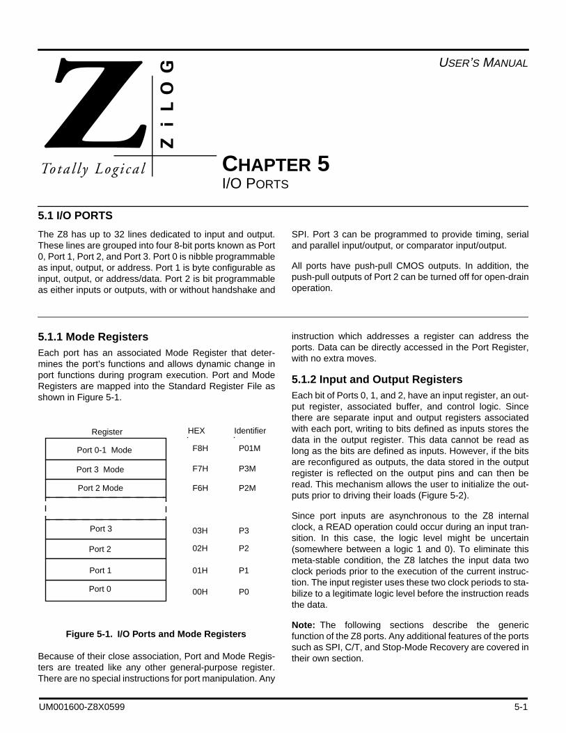
USER’S MANUAL
CHAPTER 5I/O PORTS
5.1 I/O PORTS
The Z8 has up to 32 lines dedicated to input and output.These lines are grouped into four 8-bit ports known as Port0, Port 1, Port 2, and Port 3. Port 0 is nibble programmableas input, output, or address. Port 1 is byte configurable asinput, output, or address/data. Port 2 is bit programmableas either inputs or outputs, with or without handshake and
SPI. Port 3 can be programmed to provide timing, serialand parallel input/output, or comparator input/output.
All ports have push-pull CMOS outputs. In addition, thepush-pull outputs of Port 2 can be turned off for open-drainoperation.
5.1.1 Mode RegistersEach port has an associated Mode Register that deter-mines the port’s functions and allows dynamic change inport functions during program execution. Port and ModeRegisters are mapped into the Standard Register File asshown in Figure 5-1.
Because of their close association, Port and Mode Regis-ters are treated like any other general-purpose register.There are no special instructions for port manipulation. Any
instruction which addresses a register can address theports. Data can be directly accessed in the Port Register,with no extra moves.
5.1.2 Input and Output RegistersEach bit of Ports 0, 1, and 2, have an input register, an out-put register, associated buffer, and control logic. Sincethere are separate input and output registers associatedwith each port, writing to bits defined as inputs stores thedata in the output register. This data cannot be read aslong as the bits are defined as inputs. However, if the bitsare reconfigured as outputs, the data stored in the outputregister is reflected on the output pins and can then beread. This mechanism allows the user to initialize the out-puts prior to driving their loads (Figure 5-2).
Since port inputs are asynchronous to the Z8 internalclock, a READ operation could occur during an input tran-sition. In this case, the logic level might be uncertain(somewhere between a logic 1 and 0). To eliminate thismeta-stable condition, the Z8 latches the input data twoclock periods prior to the execution of the current instruc-tion. The input register uses these two clock periods to sta-bilize to a legitimate logic level before the instruction readsthe data.
Note: The following sections describe the genericfunction of the Z8 ports. Any additional features of the portssuch as SPI, C/T, and Stop-Mode Recovery are covered intheir own section.
Figure 5-1. I/O Ports and Mode Registers
Register HEX
Port 3 Mode
Port 2 Mode
Identifier
F8H
F7H
F6H
P01M
P3M
P2M
Port 3
Port 0-1 Mode
Port 2
Port 1
Port 0
03H
02H
01H
00H
P3
P2
P1
P0
UM001600-Z8X0599 5-1

Z8 MicrocontrollersI/O Ports ZiLOG
5.2 PORT 0
This section deals with only the I/O operation of Port 0. Theport's external memory interface operation is covered later
in this manual. Figure 5-2 shows a block diagram of Port0. This diagram also applies to Ports 1 and 2.
Figure 5-2. Ports 0, 1, 2 Generic Block Diagram
Handshake Logic
InternalTiming
HandshakeSelected
RDY//DAV
/DAV/RDY
Port I/OLines
InputBuffer
InputRegister
HandshakeLogic
OutputBuffer
OutputRegister
OutputEnable
InternalBus
WritePort
ReadPort
E
88
8
8 8
8
8
5-2 UM001600-Z8X0599
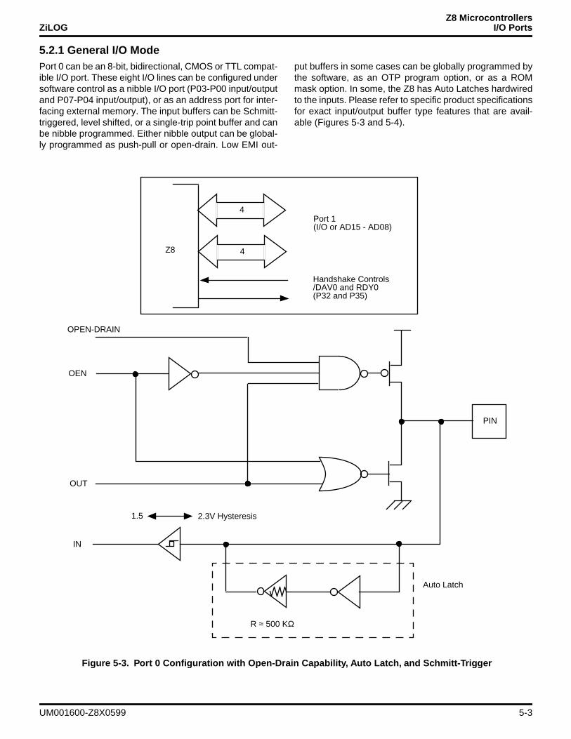
Z8 MicrocontrollersZiLOG I/O Ports
5.2.1 General I/O Mode Port 0 can be an 8-bit, bidirectional, CMOS or TTL compat-ible I/O port. These eight I/O lines can be configured undersoftware control as a nibble I/O port (P03-P00 input/outputand P07-P04 input/output), or as an address port for inter-facing external memory. The input buffers can be Schmitt-triggered, level shifted, or a single-trip point buffer and canbe nibble programmed. Either nibble output can be global-ly programmed as push-pull or open-drain. Low EMI out-
put buffers in some cases can be globally programmed bythe software, as an OTP program option, or as a ROMmask option. In some, the Z8 has Auto Latches hardwiredto the inputs. Please refer to specific product specificationsfor exact input/output buffer type features that are avail-able (Figures 5-3 and 5-4).
Figure 5-3. Port 0 Configuration with Open-Drain Capability, Auto Latch, and Schmitt-Trigger
OEN
Port 1 (I/O or AD15 - AD08)
Handshake Controls/DAV0 and RDY0
4
Z8
(P32 and P35)
PIN
OUT
IN
2.3V Hysteresis
OPEN-DRAIN
1.5
R ≈ 500 KΩ
Auto Latch
4
UM001600-Z8X0599 5-3
Z8 MicrocontrollersI/O Ports ZiLOG
5.2 PORT 0 (Continued)
5.2.2 Read/Write OperationsIn the nibble I/0 Mode, Port 0 is accessed as general-pur-pose register P0 (00H) with ERF Bank set to 0. The port iswritten by specifying P0 as an instruction's destination reg-ister. Writing to the port causes data to be stored in theport's output register.
The port is read by specifying P0 as the source register ofan instruction. When an output nibble is read, data on theexternal pins is returned. Under normal loading conditionsthis is equivalent to reading the output register. However,for Port 0 outputs defined as open–drain, the data returnedis the value forced on the output by the external system.This may not be the same as the data in the output regis-ter. Reading a nibble defined as input also returns data onthe external pins. However, input bits under handshakecontrol return data latched into the input register via the in-put strobe.
The Port 0–1 Mode resister bits D1D0 and D7D6 are usedto configure Port 0 nibbles. The lower nibble (P00–P03) canbe defined as inputs by setting bits D1 to 0 and D0 to 1, oras outputs by setting both D1 and D0 to 0. Likewise, the up-per nibble (P04–P07) can be defined as inputs by settingbits D7 to 0 and D6 to 1, or as outputs by setting both D6and D7 to 0 (Figure 5-5).
5.2.3 Handshake OperationWhen used as an I/0 port, Port 0 can be placed underhandshake control by programming the Port 3 Mode regis-ter bit D2 to 1. In this configuration, handshake control linesare DAV0 (P32) and RDY0 (P35) when Port 0 is an inputport, or RDY0 (P32) and DAV0 (P35) when Port 0 is an out-put port. (See Figure 5-6)
Handshake direction is determined by the configuration(input or output) assigned to the Port 0 upper nibble,P04–P07. The lower nibble must have the same I/0 config-uration as the upper nibble to be under handshake control.Figure 5-3 illustrates the Port 0 upper and lower nibblesand the associated handshake lines of Port 3.
Figure 5-4. Port 0 Configuration with TTL Level Shifter
OEN
PIN
OUT
IN
TTL Level Shifter
5-4 UM001600-Z8X0599
Z8 MicrocontrollersZiLOG I/O Ports
5.3 PORT 1
This section deals only with the I/0 operation. The port'sexternal memory interface operation is discussed later inthis manual. Figure 5-2 shows a block diagram of Port 1.
5.3.1 General I/O ModePort 1 can be an 8-bit, bidirectional, CMOS or TTL compat-ible port with multiplexed Address (A7–A0) and Data(D7–D0) ports. These eight I/O lines can be byte pro-grammed as inputs or outputs or can be configured undersoftware control as an Address/Data port for interfacing toexternal memory. The input buffers can be Schmitt-trig-gered, level- shifted, or a single-point buffer. In some cas-es, the output buffers can be globally programmed as ei-ther push-pull or open-drain. Low-EMI output buffers canbe globally programmed by software, as an OTP programoption, or as a ROM Mask Option. In some cases, theZ8can have auto latches hardwired to the inputs. Pleaserefer to specific product specifications for exact input/out-put buffer-type features available (Figures 5-7 and 5-8).
Figure 5-5. Port 0 I/O Operation
Figure 5-6. Port 0 Handshake Operation
D7 D6 D1 D0
(Write-Only)
01 = Input 1X = A8 - A11
P00 - P03 Mode 00 = Output
Port 0-1 Mode Register (P01M)Register F8H (P01M)
P04 - P07 Mode 00 = Output
01 = Input 1X = A12 - A15
D2
(Write-Only)
0 P32 = Input P35 = Output
Port 3 Mode Register (P3M)Register F7H
1 P32 = DAV0/RDY0 P35 = RDY0/DAV0
UM001600-Z8X0599 5-5
Z8 MicrocontrollersI/O Ports ZiLOG
5.3 PORT 1 (Continued)
Figure 5-7. Port 1 Configuration with Open-Drain Capability, Auto Latch, and Schmitt-Trigger
OEN
Port 1 (I/O or AD7 - AD0)
Handshake Controls/DAV1 and RDY1
8
Z8
(P33 and P34)
PIN
OUT
IN
2.3V Hysteresis
OPEN-DRAIN
1.5
R ≈ 500 KΩ
Auto Latch
5-6 UM001600-Z8X0599
Z8 MicrocontrollersZiLOG I/O Ports
Figure 5-8. Port 1 Configuration with TTL Level Shifter
OEN
Port 1 (I/O or AD7 - AD0)8
Z8
(P33 and P34)
PIN
OUT
IN
TTL Level Shifter
Handshake ControlsDAV1 and RDY1
UM001600-Z8X0599 5-7
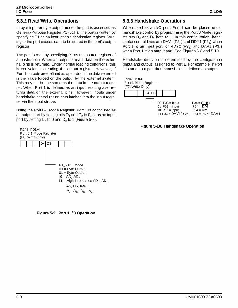
Z8 MicrocontrollersI/O Ports ZiLOG
5.3.2 Read/Write OperationsIn byte input or byte output mode, the port is accessed asGeneral-Purpose Register P1 (01H). The port is written byspecifying P1 as an instruction's destination register. Writ-ing to the port causes data to be stored in the port's outputregister.
The port is read by specifying P1 as the source register ofan instruction. When an output is read, data on the exter-nal pins is returned. Under normal loading conditions, thisis equivalent to reading the output register. However, ifPort 1 outputs are defined as open-drain, the data returnedis the value forced on the output by the external system.This may not be the same as the data in the output regis-ter. When Port 1 is defined as an input, reading also re-turns data on the external pins. However, inputs underhandshake control return data latched into the input regis-ter via the input strobe.
Using the Port 0-1 Mode Register, Port 1 is configured asan output port by setting bits D4 and D3 to 0, or as an inputport by setting D4 to 0 and D3 to 1 (Figure 5-8).
5.3.3 Handshake OperationsWhen used as an I/O port, Port 1 can be placed underhandshake control by programming the Port 3 Mode regis-ter bits D4 and D3 both to 1. In this configuration, hand-shake control lines are DAV1 (P33) and RDY1 (P34) whenPort 1 is an input port, or RDY1 (P33) and DAV1 (P34)when Port 1 is an output port. See Figures 5-8 and 5-10.
Handshake direction is determined by the configuration(input and output) assigned to Port 1. For example, if Port1 is an output port then handshake is defined as output.
Figure 5-9. Port 1 I/O Operation
D4 D3
(F8, Write-Only)
Port 0-1 Mode Register R248 P01M
01 = Byte Output
10 = AD0-AD7
00 = Byte Output P10 - P13 Mode
AS, DS, R/W, 11 = High Impedance AD0- AD7,
A8 - A11, A12 - A15
Figure 5-10. Handshake Operation
D4 D3
(F7, Write-Only)
00 P33 = Input P34 = Output 01 P33 = Input P34 = DM
Port 3 Mode RegisterR247 P3M
10 P33 = Input P34 = DM 11 P33 = DAV1/RDY1 P34 = RDY1/DAV1
5-8 UM001600-Z8X0599
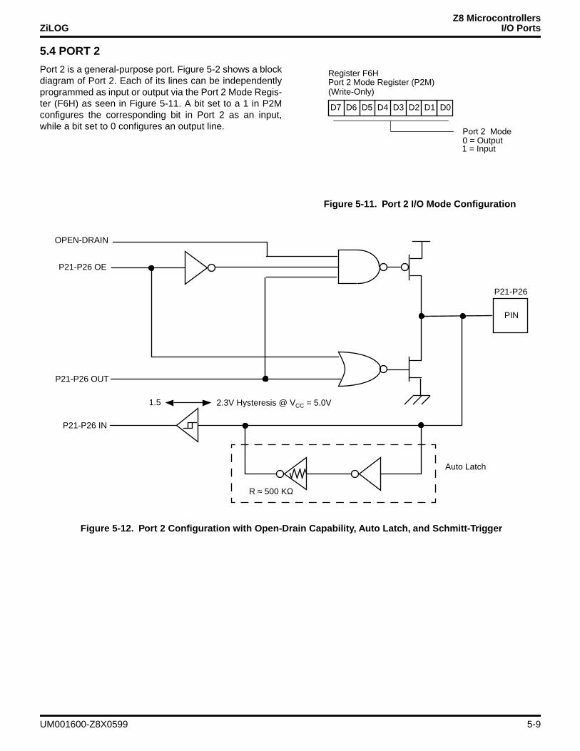
Z8 MicrocontrollersZiLOG I/O Ports
5.4 PORT 2
Port 2 is a general-purpose port. Figure 5-2 shows a blockdiagram of Port 2. Each of its lines can be independentlyprogrammed as input or output via the Port 2 Mode Regis-ter (F6H) as seen in Figure 5-11. A bit set to a 1 in P2Mconfigures the corresponding bit in Port 2 as an input,while a bit set to 0 configures an output line.
Figure 5-11. Port 2 I/O Mode Configuration
D7 D6 D5 D4 D3 D2 D1 D0
(Write-Only)
1 = Input
Port 2 Mode 0 = Output
Port 2 Mode Register (P2M)Register F6H
Figure 5-12. Port 2 Configuration with Open-Drain Capability, Auto Latch, and Schmitt-Trigger
P21-P26 OE
PIN
P21-P26 OUT
P21-P26 IN
2.3V Hysteresis @ VCC = 5.0V
OPEN-DRAIN
1.5
R ≈ 500 KΩ
Auto Latch
P21-P26
UM001600-Z8X0599 5-9
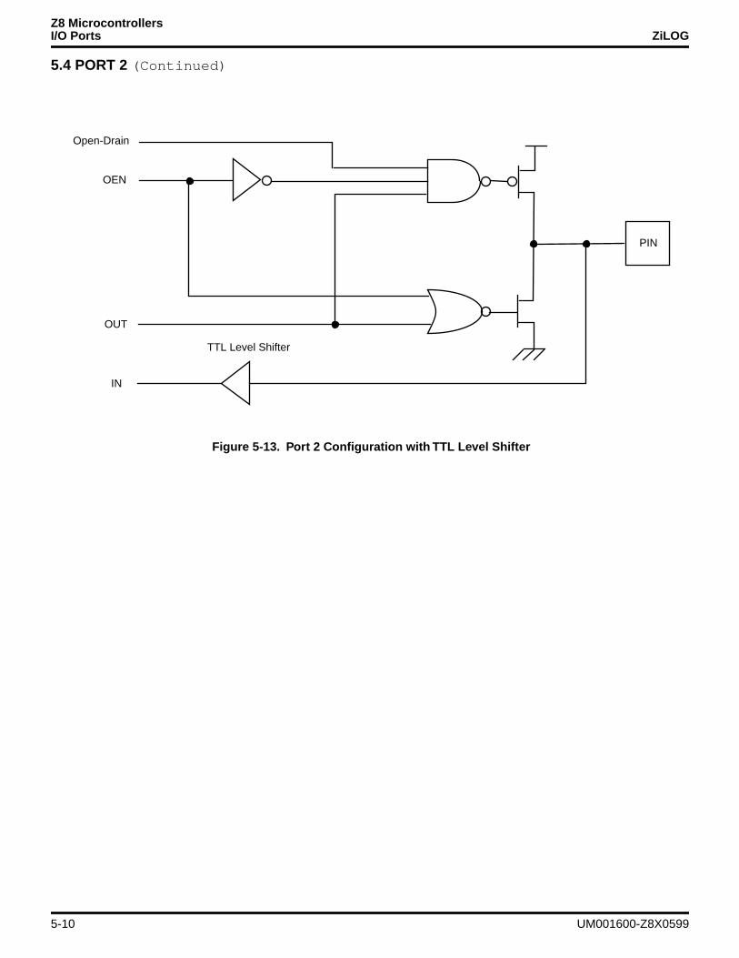
Z8 MicrocontrollersI/O Ports ZiLOG
5.4 PORT 2 (Continued)
Figure 5-13. Port 2 Configuration with TTL Level Shifter
OEN
PIN
OUT
IN
TTL Level Shifter
Open-Drain
5-10 UM001600-Z8X0599
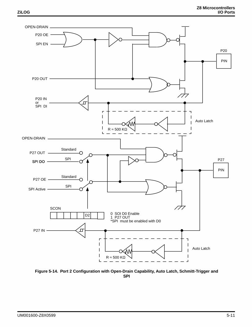
Z8 MicrocontrollersZiLOG I/O Ports
Figure 5-14. Port 2 Configuration with Open-Drain Capability, Auto Latch, Schmitt-Trigger and SPI
P27 OUT
PIN
SPI Active
P27 IN
0 SOI D0 Enable
OPEN-DRAIN
R ≈ 500 KΩ
Auto Latch
P27
P20 OE
PIN
P20 OUT
P20 IN
OPEN-DRAIN
R ≈ 500 KΩ
Auto Latch
P20
SPI EN
SPI DO
P27 OE
SPI
SPI DOSPI
Standard
Standard
1 P27 OUT*SPI must be enabled with D0
D2
SCON
orSPI DI
UM001600-Z8X0599 5-11
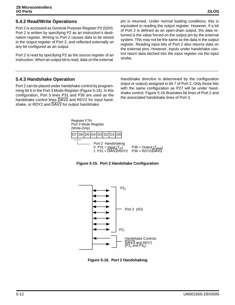
Z8 MicrocontrollersI/O Ports ZiLOG
5.4.2 Read/Write OperationsPort 2 is accessed as General-Purpose Register P2 (02H).Port 2 is written by specifying P2 as an instruction’s desti-nation register. Writing to Port 2 causes data to be storedin the output register of Port 2, and reflected externally onany bit configured as an output.
Port 2 is read by specifying P2 as the source register of aninstruction. When an output bit is read, data on the external
pin is returned. Under normal loading conditions, this isequivalent to reading the output register. However, if a bitof Port 2 is defined as an open-drain output, the data re-turned is the value forced on the output pin by the externalsystem. This may not be the same as the data in the outputregister. Reading input bits of Port 2 also returns data onthe external pins. However, inputs under handshake con-trol return data latched into the input register via the inputstrobe.
5.4.3 Handshake OperationPort 2 can be placed under handshake control by program-ming bit 6 in the Port 3 Mode Register (Figure 5-15). In thisconfiguration, Port 3 lines P31 and P36 are used as thehandshake control lines DAV2 and RDY2 for input hand-shake, or RDY2 and DAV2 for output handshake.
Handshake direction is determined by the configuration(input or output) assigned to bit 7 of Port 2. Only those bitswith the same configuration as P27 will be under hand-shake control. Figure 5-16 illustrates bit lines of Port 2 andthe associated handshake lines of Port 3.
Figure 5-15. Port 2 Handshake Configuration
D7 D6 D5 D4 D3 D2 D1 D0
(Write-Only)Port 3 Mode RegisterRegister F7H
1 P31 = DAV2/RDY2 P36 = RDY2/DAV2
0 P31 = Input (TIN) P36 = Output (TOUT) Port 2 Handshaking
Figure 5-16. Port 2 Handshaking
Handshake ControlsDAV2 and RDY2(P31 and P36)
P27
Port 2 (I/O)
P20
5-12 UM001600-Z8X0599
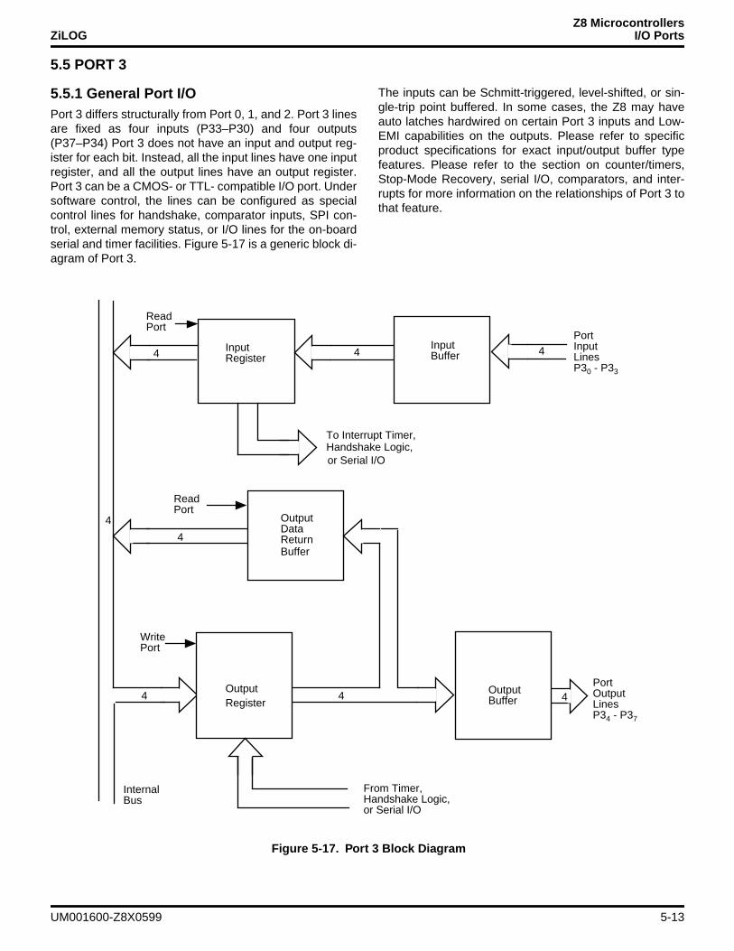
Z8 MicrocontrollersZiLOG I/O Ports
5.5 PORT 3
5.5.1 General Port I/OPort 3 differs structurally from Port 0, 1, and 2. Port 3 linesare fixed as four inputs (P33–P30) and four outputs(P37–P34) Port 3 does not have an input and output reg-ister for each bit. Instead, all the input lines have one inputregister, and all the output lines have an output register.Port 3 can be a CMOS- or TTL- compatible I/O port. Undersoftware control, the lines can be configured as specialcontrol lines for handshake, comparator inputs, SPI con-trol, external memory status, or I/O lines for the on-boardserial and timer facilities. Figure 5-17 is a generic block di-agram of Port 3.
The inputs can be Schmitt-triggered, level-shifted, or sin-gle-trip point buffered. In some cases, the Z8 may haveauto latches hardwired on certain Port 3 inputs and Low-EMI capabilities on the outputs. Please refer to specificproduct specifications for exact input/output buffer typefeatures. Please refer to the section on counter/timers,Stop-Mode Recovery, serial I/O, comparators, and inter-rupts for more information on the relationships of Port 3 tothat feature.
Figure 5-17. Port 3 Block Diagram
InputBufferInput
Register
OutputBuffer
OutputRegister
OutputRegister
WritePort
ReadPort
4
4
4
4
4 4
4 4
InternalBus
From Timer,Handshake Logic,or Serial I/O
To Interrupt Timer,Handshake Logic,or Serial I/O
PortOutputLinesP34 - P37
PortInputLinesP30 - P33
ReadPort
InputBuffer
Output
Buffer
OutputRegister
OutputBuffer
DataReturn
UM001600-Z8X0599 5-13
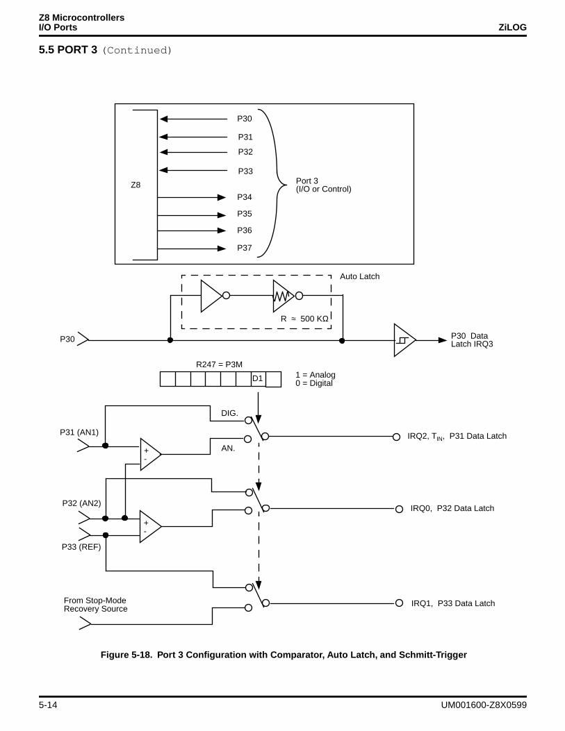
Z8 MicrocontrollersI/O Ports ZiLOG
5.5 PORT 3 (Continued)
Figure 5-18. Port 3 Configuration with Comparator, Auto Latch, and Schmitt-Trigger
P31 (AN1)
R247 = P3M
+-
IRQ2, TIN, P31 Data Latch
P30
+-
1 = Analog0 = Digital D1
R ≈ 500 KΩ
Auto Latch
Port 3(I/O or Control)
P30 DataLatch IRQ3
Z8
P34
P35
P37
P36
P30
P31
P32
P33
IRQ0, P32 Data Latch
IRQ1, P33 Data Latch
P32 (AN2)
P33 (REF)
From Stop-ModeRecovery Source
DIG.
AN.
5-14 UM001600-Z8X0599
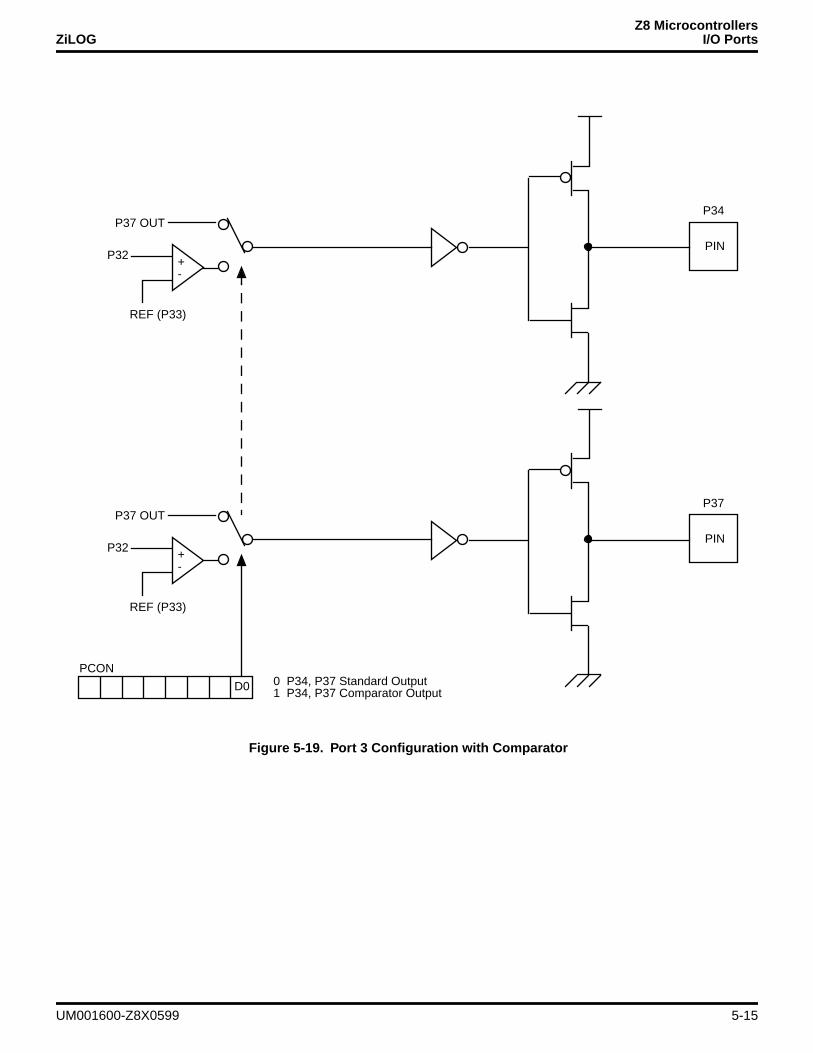
Z8 MicrocontrollersZiLOG I/O Ports
Figure 5-19. Port 3 Configuration with Comparator
PIN
P37
0 P34, P37 Standard Output1 P34, P37 Comparator Output D0
P37 OUT
PCON
P32
REF (P33)
+-
PIN
P34P37 OUT
P32
REF (P33)
+-
UM001600-Z8X0599 5-15
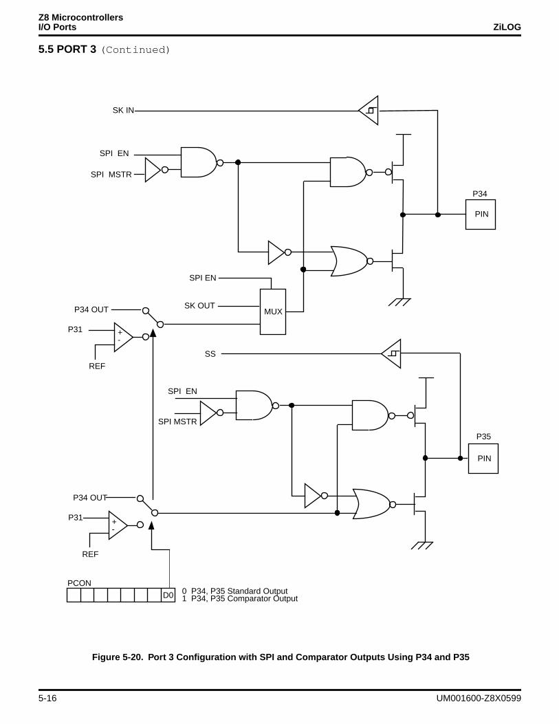
Z8 MicrocontrollersI/O Ports ZiLOG
5.5 PORT 3 (Continued)
Figure 5-20. Port 3 Configuration with SPI and Comparator Outputs Using P34 and P35
SPI MSTR
PIN
P31 +
SPI EN
P34
SK IN
SPI MSTR
PIN
P35
SPI EN
REF
SS
0 P34, P35 Standard Output1 P34, P35 Comparator Output D0
P34 OUT
PCON
P31
REF
+-
P34 OUT
-
SPI EN
SK OUTMUX
5-16 UM001600-Z8X0599
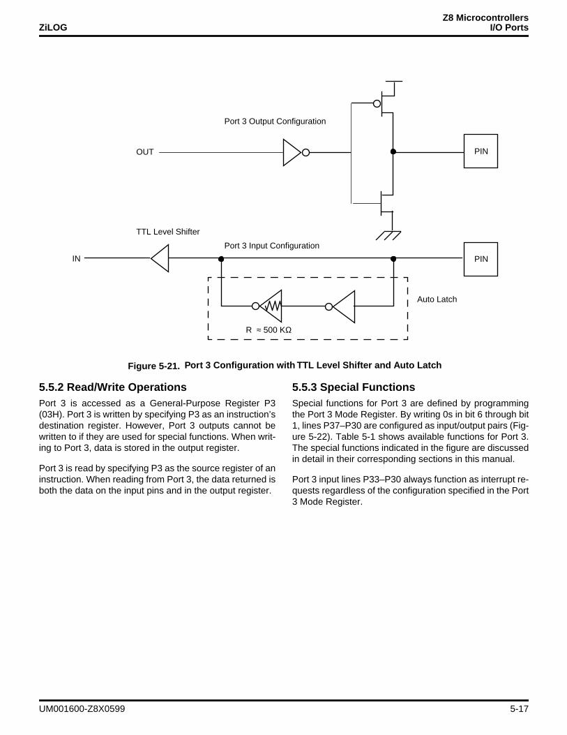
Z8 MicrocontrollersZiLOG I/O Ports
5.5.2 Read/Write OperationsPort 3 is accessed as a General-Purpose Register P3(03H). Port 3 is written by specifying P3 as an instruction’sdestination register. However, Port 3 outputs cannot bewritten to if they are used for special functions. When writ-ing to Port 3, data is stored in the output register.
Port 3 is read by specifying P3 as the source register of aninstruction. When reading from Port 3, the data returned isboth the data on the input pins and in the output register.
5.5.3 Special FunctionsSpecial functions for Port 3 are defined by programmingthe Port 3 Mode Register. By writing 0s in bit 6 through bit1, lines P37–P30 are configured as input/output pairs (Fig-ure 5-22). Table 5-1 shows available functions for Port 3.The special functions indicated in the figure are discussedin detail in their corresponding sections in this manual.
Port 3 input lines P33–P30 always function as interrupt re-quests regardless of the configuration specified in the Port3 Mode Register.
Figure 5-21. Port 3 Configuration with TTL Level Shifter and Auto Latch
PIN
PINOUT
R ≈ 500 KΩ
Auto Latch
IN
TTL Level Shifter
Port 3 Output Configuration
Port 3 Input Configuration
UM001600-Z8X0599 5-17
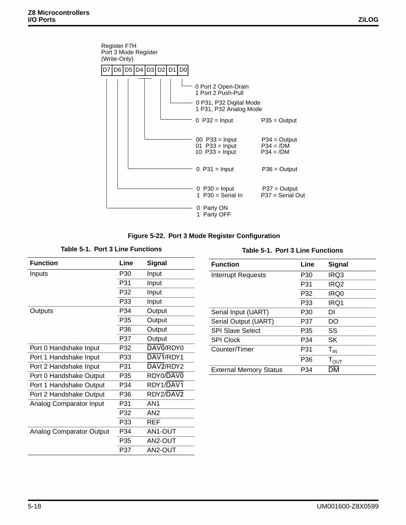
Z8 MicrocontrollersI/O Ports ZiLOG
Figure 5-22. Port 3 Mode Register Configuration
D7 D6 D5 D4 D3 D2 D1 D0
(Write-Only)
0 P31, P32 Digital Mode 1 P31, P32 Analog Mode
0 P32 = Input P35 = Output
0 Port 2 Open-Drain 1 Port 2 Push-Pull
00 P33 = Input P34 = Output 01 P33 = Input P34 = /DM
Port 3 Mode RegisterRegister F7H
10 P33 = Input P34 = /DM
0 P31 = Input P36 = Output
0 P30 = Input P37 = Output 1 P30 = Serial In P37 = Serial Out
0 Party ON 1 Party OFF
Table 5-1. Port 3 Line Functions
Function Line Signal
Inputs P30 InputP31 InputP32 InputP33 Input
Outputs P34 OutputP35 OutputP36 OutputP37 Output
Port 0 Handshake Input P32 DAV0/RDY0Port 1 Handshake Input P33 DAV1/RDY1Port 2 Handshake Input P31 DAV2/RDY2Port 0 Handshake Output P35 RDY0/DAV0Port 1 Handshake Output P34 RDY1/DAV1Port 2 Handshake Output P36 RDY2/DAV2Analog Comparator Input P31 AN1
P32 AN2P33 REF
Analog Comparator Output P34 AN1-OUTP35 AN2-OUTP37 AN2-OUT
Interrupt Requests P30 IRQ3P31 IRQ2P32 IRQ0P33 IRQ1
Serial Input (UART) P30 DISerial Output (UART) P37 DOSPI Slave Select P35 SSSPI Clock P34 SKCounter/Timer P31 TIN
P36 TOUT
External Memory Status P34 DM
Table 5-1. Port 3 Line Functions
Function Line Signal
5-18 UM001600-Z8X0599
Z8 MicrocontrollersZiLOG I/O Ports
5.6 PORT HANDSHAKE
When Ports 0, 1, and 2 are configured for handshake op-eration, a pair of lines from Port 3 are used for handshakecontrols. The handshake controls are interlocked to prop-erly time asynchronous data transfers between the Z8®and a peripheral. One control line (/DAV) functions as astrobe from the sender to indicate to the receiver that datais available. The second control line (RDY) acknowledgesreceipt of the sender’s data, and indicates when the receiv-er is ready to accept another data transfer.
In the input mode, data is latched into the Port’s input reg-ister by the first /DAV signal, and is protected from beingoverwritten if additional pulses occur on the /DAV line. Thisoverwrite protection is maintained until the port data isread. In the output mode, data written to the port is not pro-tected and can be overwritten by the Z8 during the hand-shake sequence. To avoid losing data, the software mustnot overwrite the port until the corresponding interrupt re-quest indicates that the external device has latched the da-ta.
The software can always read Port 3 output and inputhandshake lines, but cannot write to the output handshakeline.
The following is the recommended setup sequence whenconfiguring a Port for handshake operation for the first timeafter a reset:
• Load P01M or P2M to configure the port for input/output.
• Load P3 to set the Output Handshake bit to a logic 1.
• Load P3M to select the Handshake Mode for the port.
Once a data transfer begins, the configuration of the hand-shake lines should not be changed until the handshake iscompleted.
Figures 5-23 and 5-24 show detailed operation for thehandshake sequence.
UM001600-Z8X0599 5-19
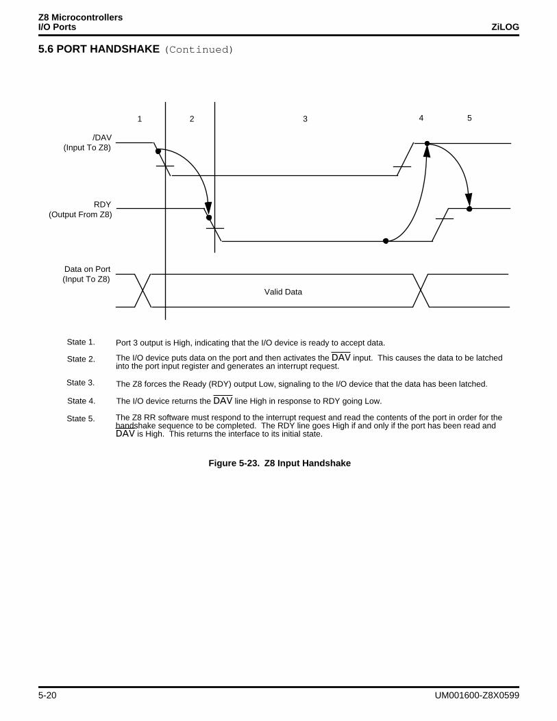
Z8 MicrocontrollersI/O Ports ZiLOG
5.6 PORT HANDSHAKE (Continued)
Figure 5-23. Z8 Input Handshake
Valid Data
(Input To Z8)
State 1.
21 3 4 5
/DAV
(Output From Z8) RDY
(Input To Z8)Data on Port
Port 3 output is High, indicating that the I/O device is ready to accept data.
State 2. The I/O device puts data on the port and then activates the DAV input. This causes the data to be latched.
State 3. The Z8 forces the Ready (RDY) output Low, signaling to the I/O device that the data has been latched.
State 4. The I/O device returns the DAV line High in response to RDY going Low.
State 5. The Z8 RR software must respond to the interrupt request and read the contents of the port in order for the
into the port input register and generates an interrupt request.
handshake sequence to be completed. The RDY line goes High if and only if the port has been read andDAV is High. This returns the interface to its initial state.
5-20 UM001600-Z8X0599
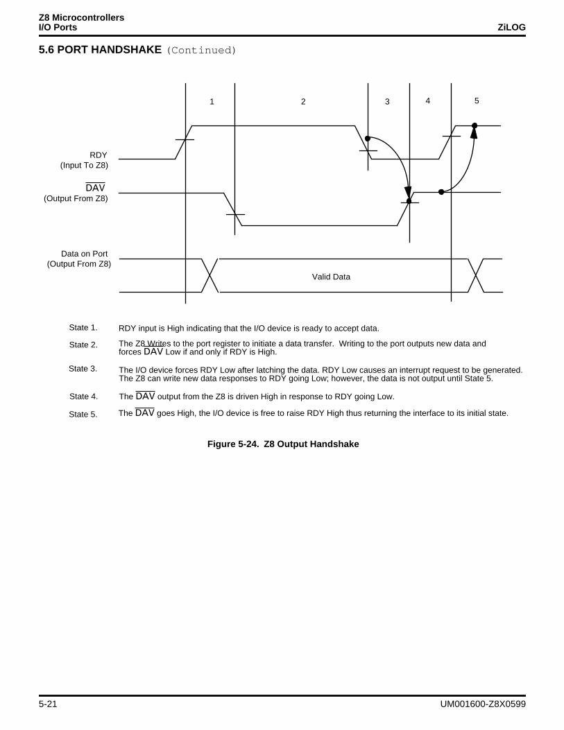
Z8 MicrocontrollersI/O Ports ZiLOG
5.6 PORT HANDSHAKE (Continued)
Figure 5-24. Z8 Output Handshake
Valid Data
(Input To Z8)
State 1.
21 3 4 5
RDY
(Output From Z8) DAV
(Output From Z8)Data on Port
RDY input is High indicating that the I/O device is ready to accept data.
State 2. The Z8 Writes to the port register to initiate a data transfer. Writing to the port outputs new data andforces DAV Low if and only if RDY is High.
State 3. The I/O device forces RDY Low after latching the data. RDY Low causes an interrupt request to be generated.The Z8 can write new data responses to RDY going Low; however, the data is not output until State 5.
State 4. The DAV output from the Z8 is driven High in response to RDY going Low.
State 5. The DAV goes High, the I/O device is free to raise RDY High thus returning the interface to its initial state.
5-21 UM001600-Z8X0599
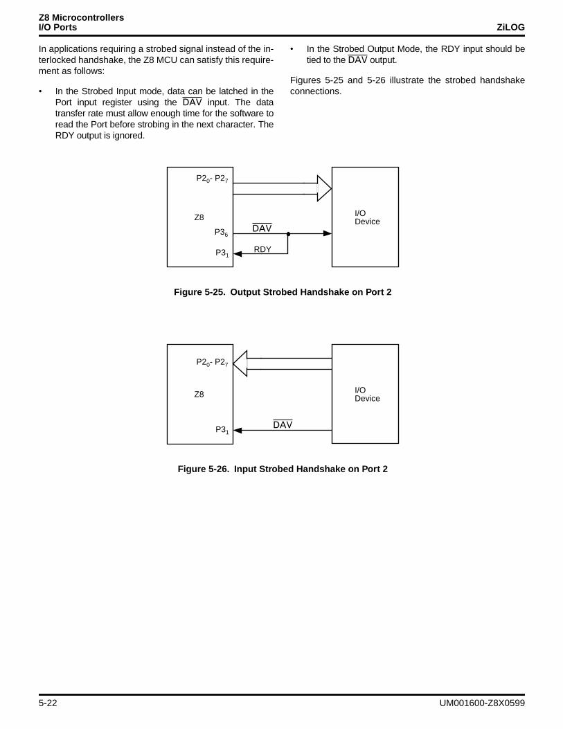
Z8 MicrocontrollersI/O Ports ZiLOG
In applications requiring a strobed signal instead of the in-terlocked handshake, the Z8 MCU can satisfy this require-ment as follows:
• In the Strobed Input mode, data can be latched in thePort input register using the DAV input. The datatransfer rate must allow enough time for the software toread the Port before strobing in the next character. TheRDY output is ignored.
• In the Strobed Output Mode, the RDY input should betied to the DAV output.
Figures 5-25 and 5-26 illustrate the strobed handshakeconnections.
Figure 5-25. Output Strobed Handshake on Port 2
P36
Z8
P20- P27
P31
I/ODevice
DAV
RDY
Figure 5-26. Input Strobed Handshake on Port 2
Z8
P20- P27
P31
I/ODevice
DAV
5-22 UM001600-Z8X0599
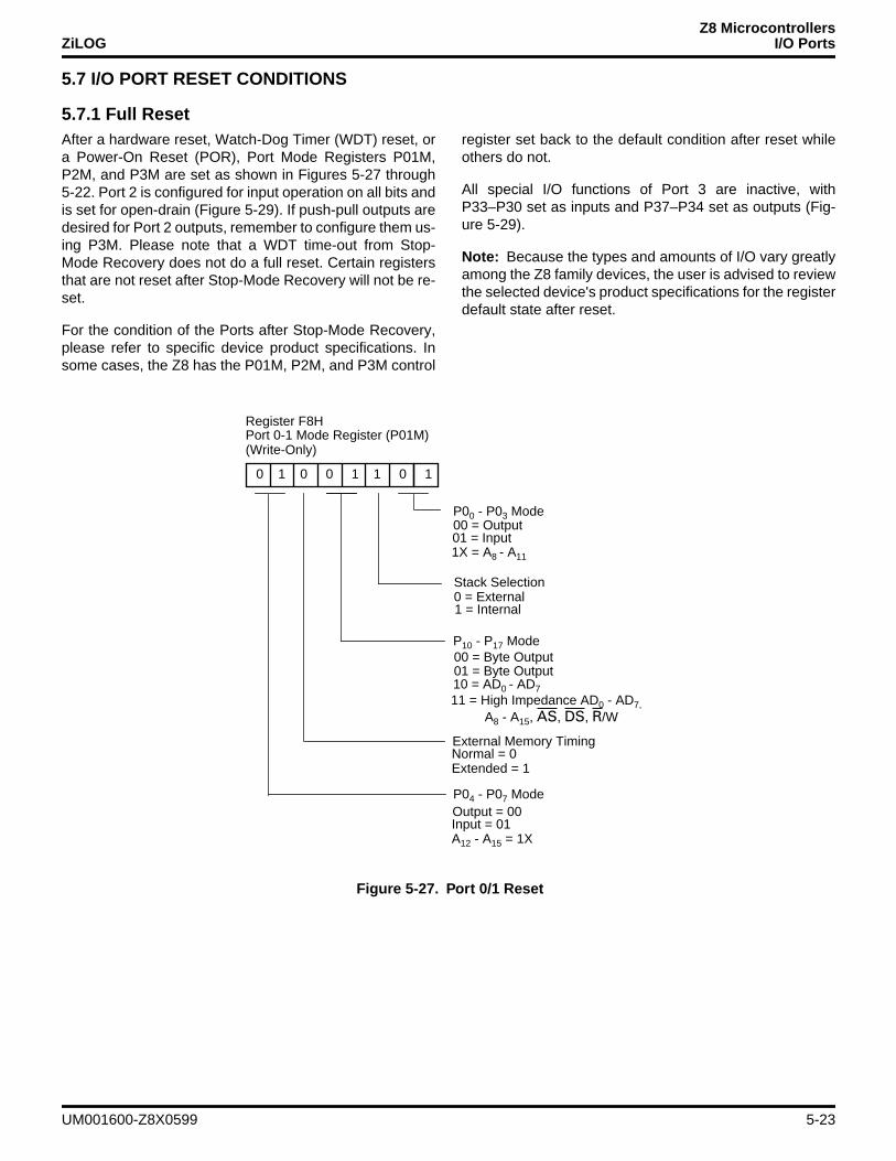
Z8 MicrocontrollersZiLOG I/O Ports
5.7 I/O PORT RESET CONDITIONS
5.7.1 Full ResetAfter a hardware reset, Watch-Dog Timer (WDT) reset, ora Power-On Reset (POR), Port Mode Registers P01M,P2M, and P3M are set as shown in Figures 5-27 through5-22. Port 2 is configured for input operation on all bits andis set for open-drain (Figure 5-29). If push-pull outputs aredesired for Port 2 outputs, remember to configure them us-ing P3M. Please note that a WDT time-out from Stop-Mode Recovery does not do a full reset. Certain registersthat are not reset after Stop-Mode Recovery will not be re-set.
For the condition of the Ports after Stop-Mode Recovery,please refer to specific device product specifications. Insome cases, the Z8 has the P01M, P2M, and P3M control
register set back to the default condition after reset whileothers do not.
All special I/O functions of Port 3 are inactive, withP33–P30 set as inputs and P37–P34 set as outputs (Fig-ure 5-29).
Note: Because the types and amounts of I/O vary greatlyamong the Z8 family devices, the user is advised to reviewthe selected device's product specifications for the registerdefault state after reset.
Figure 5-27. Port 0/1 Reset
0 1 0 0 1 1 0 1
(Write-Only)
01 = Input 1X = A8 - A11
Stack Selection 0 = External
P00 - P03 Mode 00 = Output
Port 0-1 Mode Register (P01M)Register F8H
01 = Byte Output
1 = Internal
External Memory Timing Normal = 0 Extended = 1
P04 - P07 Mode Output = 00
Input = 01 A12 - A15 = 1X
10 = AD0 - AD7
00 = Byte Output P10 - P17 Mode
A8 - A15, AS, DS, R/W 11 = High Impedance AD0 - AD7,
UM001600-Z8X0599 5-23

Z8 MicrocontrollersI/O Ports ZiLOG
Figure 5-28. Port 2 Reset
1 1 1 1 1 1 1 1
(Write-Only)
1 = Input
Port 2 Mode 0 = Output
Port 2 Mode Register (P2M)Register F6H
Figure 5-29. Port 3 Mode Reset
0 0 0 0 0 0 0 0
(Write-Only)
0 P31, P32 Digital Mode 1 P31, P32 Analog Mode
0 P32 = Input P35 = Output 1 P32 = DAV0/RDY0 P35 = RDY0/DAV0
0 Port 2 Open-Drain 1 Port 2 Push-Pull
00 P33 = Input P34 = Output 01 P33 = Input P34 = DM
Port 3 Mode Register (P3M)Register F7H
10 P33 = Input P34 = DM 11 P33 = DAV1/RDY1 P34 = RDY1/DAV1
0 P31 = Input P36 = Output 1 P32 = DAV2/RDY2 P36 = RDY2/DAV2
0 P30 = Input P37 = Output 1 P30 = Serial In P37 = Serial Out
0 Parity OFF 1 Parity ON
5-24 UM001600-Z8X0599
Z8 MicrocontrollersI/O Ports ZiLOG
5.8 ANALOG COMPARATORS (Continued)
5.8 ANALOG COMPARATORS
Select Z8 devices include two independent on-chip analogcomparators. See the device product specification for fea-ture availability and use. Port 3, Pins P31 and P32 eachhave a comparator front end. The comparator referencevoltage, pin P33, is common to both comparators. In Ana-log Mode, the P31 and P32 are the positive inputs to thecomparators and P33 is the reference voltage supplied toboth comparators. In Digital Mode, pin P33 can be used asa P33 register input or IRQ1 source. P34, P35, or P37 mayoutput the comparator outputs by software-programmingthe PCON Register bit D0 to 1.
5.8.1 Comparator DescriptionTwo on-board comparators can process analog signals onP31 and P32 with reference to the voltage on P33. The an-alog function is enabled by programming the Port 3 ModeRegister (P3M bit 1). For interrupt functions during analogmode, P31 and P32 can be programmable as rising, fall-ing, or both edge triggered interrupts (IRQ register bits 6and bit 7).
Note: P33 cannot generate an external interrupt while inthis mode. P33 can only generate interrupts in the DigitalMode.
Note: Port 3 inputs must be in digital mode if Port 3 is aStop-Mode Recovery source. The analog comparator isdisabled in STOP mode.
P31 can be used as TIN in Analog or Digital Modes, but itmust be referenced to P33, when in Analog Mode.
Figure 5-30. Port 3 Input Analog Selection
D1
(Write-Only)
0 = Digital Mode P31, P32, P33 1 = Analog Mode P31, P32, P33
Port 3 Mode Register (P3M)Register F7H
Figure 5-31. Port 3 Comparator Output Selection
D0
(Write-Only)
0 = P34, P35, or P37 Standard Outputs 1 = P34, P35, or P37 Comparator Outputs
Port Configuration Register (PCON)Register 00H
ERF Bank F
5-25 UM001600-Z8X0599
Z8 MicrocontrollersI/O Ports ZiLOG
Figure 5-32. Port Configuration of Comparator Inputs on P31, P32, and P33
P31 (AN1)
R247 = P3M
+-
IRQ2, TIN, P31 Data Latch
P30
+-
1 = Analog0 = Digital D1
R ≈ 500 KΩ
Auto Latch
Port 3(I/O or Control)
P30 DataLatch IRQ3
Z8
P34
P35
P37
P36
P30
P31
P32
P33
IRQ0, P32 Data Latch
IRQ1, P33 Data Latch
P32 (AN2)
P33 (REF)
From Stop-ModeRecovery Source
DIG.
AN.
5-26 UM001600-Z8X0599
Z8 MicrocontrollersZiLOG I/O Ports
5.8.2 Comparator ProgrammingExample of enabling analog comparator mode.
Note: X = Any Binary Number
Example of enabling analog comparator output.
Figure 5-33. Port 3 Configuration
PIN
P37
0 P34, P37 Standard Output1 P34, P37 Comparator Output D0
P37 OUT
PCON
P32
REF (P33)
+-
PIN
P34P34 OUT
P31
REF (P33)
+-
LD P3M, #XXXX XX1XB
LD RP, #%0FH ;Sets register pointer to ;working register group 0 ;and Expanded Register ;File Bank F.
LD R0, #XXXX XXX1B ;Enables comparator;outputs using PCON
;Register programming.
UM001600-Z8X0599 5-27
Z8 MicrocontrollersI/O Ports ZiLOG
5.8.3 COMPARATOR OPERATIONAfter enabling the Analog Comparator mode, P33 be-comes a common reference input for both comparators.The P33 (Ref) is hard wired to the reference inputs to bothcomparators and cannot be separated. P31 and P32 arealways connected to the positive inputs to the compara-tors. P31 is the positive input to comparator AN1 while P32is the positive input to comparator AN2. The outputs tocomparators AN1 and AN2 are AN1-out and AN2-out, re-spectively.
The comparator output reflects the relationship betweenthe positive input to the reference input.
Example: If the voltage on AN1 is higher than the voltageon Ref then AN1-out will be at a high state. If voltage onAN2 is lower than the voltage on Ref then AN2-out will beat a Low state. In this example, when the Port 3 register isread, Bits D1 = 1 and D2 = 0. If the comparator outputs areenabled to come out on P34 and P37, then P34 = 1 andP37 = 0. Please note that the previous data stored in P34and P37 is not disturbed. Once the comparator outputs arede-selected the stored values in the P34 and P37 registerbits will be reflected on these pins again.
5.8.4 InterruptsIn the example from Section 5.8.3, P32 (AN2) will generatean interrupt based on the result of the comparison beinglow and the Interrupt Request Register (IRQ FAH) havingbits D7=0 and D6=0. If IRQ D7=1 and D6=0 then both P31and P32 would generate interrupts.
5.8.5 Comparator Definitions5.8.5.1 VICR
The usable voltage range for both positive inputs and thereference input is called the common mode voltage range(VICR). The comparator is not guaranteed to work if the in-puts are outside of the VICR range.
5.8.5.2 VOFFSET
The absolute value of the voltage between the positive in-put and the reference input required to make the compar-ator output voltage switch is the input offset voltage (VOFF-
SET). If AN1 is 3.000V and Ref is 3.001V when thecomparator output switches states then the Voffset = 1mV.
5.8.5.3 IIOFor CMOS voltage comparator inputs, the input offset cur-rent (IIO) is the leakage current of the CMOS input gate.
5.8.6 RUN ModeP33 is not available as an interrupt input during AnalogMode. P31 and P32 are valid interrupt inputs in conjunc-tion with P33 (Ref) when in the Analog Mode.
P31 can still be used as TIN when the analog mode is se-lected. If comparator outputs are desired to be outputtedon the Port 3 outputs, please refer to specific productsspecification for priority of mixing when other special fea-tures are sharing those same Port 3 pins.
5.8.7 HALT ModeThe analog comparators are functional during HALT Modeif the Analog Mode has been enabled. P31 and P32, inconjunction with P33 (Ref) will be able to generate inter-rupts. Only P33 cannot generate an interrupt since the P33input goes directly to the Ref input of the comparators andis disconnected from the interrupt sensing circuits.
5.8.8 STOP ModeThe analog comparators are disabled during STOP Modeso it does not use any current at that time. If P31, P32, orP33 are used as a source for Stop-Mode Recovery, thePort 3 Digital Mode must be selected by setting bit D1=0 inthe Port 3 Mode Register. Otherwise in STOP Mode, theP31, P32, and P33 cannot be sensed. If the Analog Modewas selected when entering STOP Mode, it will still be en-abled after a valid SMR triggered reset.
5-28 UM001600-Z8X0599
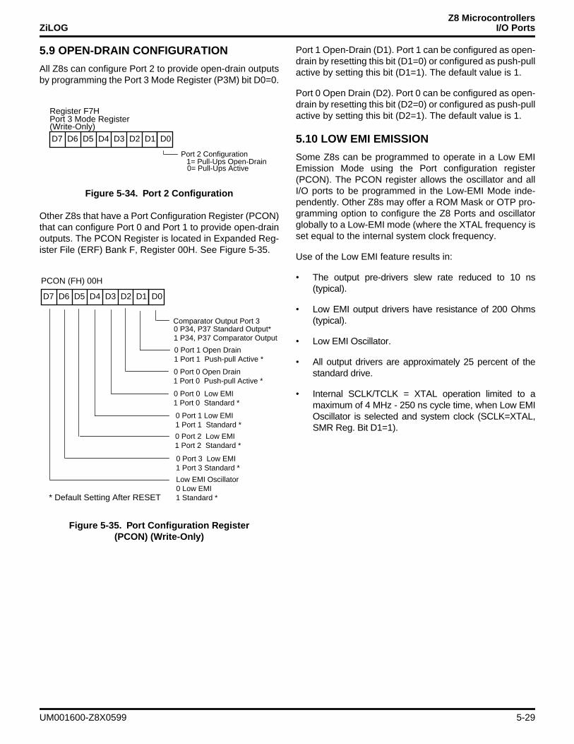
Z8 MicrocontrollersZiLOG I/O Ports
5.9 OPEN-DRAIN CONFIGURATION
All Z8s can configure Port 2 to provide open-drain outputsby programming the Port 3 Mode Register (P3M) bit D0=0.
Other Z8s that have a Port Configuration Register (PCON)that can configure Port 0 and Port 1 to provide open-drainoutputs. The PCON Register is located in Expanded Reg-ister File (ERF) Bank F, Register 00H. See Figure 5-35.
Port 1 Open-Drain (D1). Port 1 can be configured as open-drain by resetting this bit (D1=0) or configured as push-pullactive by setting this bit (D1=1). The default value is 1.
Port 0 Open Drain (D2). Port 0 can be configured as open-drain by resetting this bit (D2=0) or configured as push-pullactive by setting this bit (D2=1). The default value is 1.
5.10 LOW EMI EMISSION
Some Z8s can be programmed to operate in a Low EMIEmission Mode using the Port configuration register(PCON). The PCON register allows the oscillator and allI/O ports to be programmed in the Low-EMI Mode inde-pendently. Other Z8s may offer a ROM Mask or OTP pro-gramming option to configure the Z8 Ports and oscillatorglobally to a Low-EMI mode (where the XTAL frequency isset equal to the internal system clock frequency.
Use of the Low EMI feature results in:
• The output pre-drivers slew rate reduced to 10 ns(typical).
• Low EMI output drivers have resistance of 200 Ohms(typical).
• Low EMI Oscillator.
• All output drivers are approximately 25 percent of thestandard drive.
• Internal SCLK/TCLK = XTAL operation limited to amaximum of 4 MHz - 250 ns cycle time, when Low EMIOscillator is selected and system clock (SCLK=XTAL,SMR Reg. Bit D1=1).
Figure 5-34. Port 2 Configuration
Figure 5-35. Port Configuration Register (PCON) (Write-Only)
D7 D6 D5 D4 D3 D2 D1 D0(Write-Only)
0= Pull-Ups Active
Port 2 Configuration 1= Pull-Ups Open-Drain
Port 3 Mode RegisterRegister F7H
D7 D6 D5 D4 D3 D2 D1 D0
PCON (FH) 00H
0 Port 1 Open Drain 1 Port 1 Push-pull Active *
0 P34, P37 Standard Output* 1 P34, P37 Comparator Output
Comparator Output Port 3
Low EMI Oscillator
0 Port 0 Open Drain 1 Port 0 Push-pull Active *
0 Port 0 Low EMI 1 Port 0 Standard *
0 Port 1 Low EMI 1 Port 1 Standard *
0 Port 2 Low EMI 1 Port 2 Standard *
0 Low EMI 1 Standard *
0 Port 3 Low EMI 1 Port 3 Standard *
* Default Setting After RESET
UM001600-Z8X0599 5-29
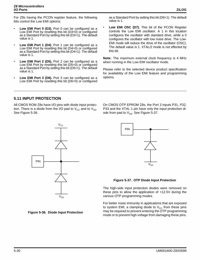
Z8 MicrocontrollersI/O Ports ZiLOG
For Z8s having the PCON register feature, the followingbits control the Low EMI options:
• Low EMI Port 0 (D3). Port 0 can be configured as aLow EMI Port by resetting this bit (D3=0) or configuredas a Standard Port by setting this bit (D3=1). The defaultvalue is 1.
• Low EMI Port 1 (D4) . Port 1 can be configured as aLow EMI Port by resetting this bit (D4=0) or configuredas a Standard Port by setting this bit (D4=1). The defaultvalue is 1.
• Low EMI Port 2 (D5). Port 2 can be configured as aLow EMI Port by resetting this bit (D5=0) or configuredas a Standard Port by setting this bit (D5=1). The defaultvalue is 1.
• Low EMI Port 3 (D6). Port 3 can be configured as aLow EMI Port by resetting this bit (D6=0) or configured
as a Standard Port by setting this bit (D6=1). The defaultvalue is 1.
• Low EMI OSC (D7). This bit of the PCON Registercontrols the Low EMI oscillator. A 1 in this locationconfigures the oscillator with standard drive, while a 0configures the oscillator with low noise drive. The Low-EMI mode will reduce the drive of the oscillator (OSC).The default value is 1. XTAL/2 mode is not effected bythis bit.
Note: The maximum external clock frequency is 4 MHzwhen running in the Low EMI oscillator mode.
Please refer to the selected device product specificationfor availability of the Low EMI feature and programmingoptions.
5.11 INPUT PROTECTION
All CMOS ROM Z8s have I/O pins with diode input protec-tion. There is a diode from the I/O pad to VCC and to VSS.See Figure 5-36.
On CMOS OTP EPROM Z8s, the Port 3 inputs P31, P32,P33 and the XTAL 1 pin have only the input protection di-ode from pad to VSS. See Figure 5-37.
The high-side input protection diodes were removed onthese pins to allow the application of +12.5V during thevarious OTP programming modes.
For better noise immunity in applications that are exposedto system EMI, a clamping diode to VCC from these pinsmay be required to prevent entering the OTP programmingmode or to prevent high voltage from damaging these pins.
Figure 5-36. Diode Input Protection
PIN
VCC
VSS
Figure 5-37. OTP Diode Input Protection
PIN
VSS
5-30 UM001600-Z8X0599
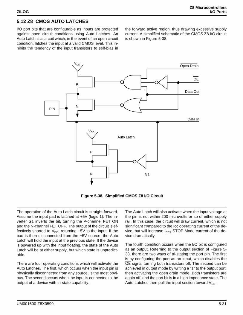
Z8 MicrocontrollersZiLOG I/O Ports
5.12 Z8 CMOS AUTO LATCHES
I/O port bits that are configurable as inputs are protectedagainst open circuit conditions using Auto Latches. AnAuto Latch is a circuit which, in the event of an open circuitcondition, latches the input at a valid CMOS level. This in-hibits the tendency of the input transistors to self-bias in
the forward active region, thus drawing excessive supplycurrent. A simplified schematic of the CMOS Z8 I/O circuitis shown in Figure 5-38.
The operation of the Auto Latch circuit is straight-forward.Assume the input pad is latched at +5V (logic 1). The in-verter G1 inverts the bit, turning the P-channel FET ONand the N-channel FET OFF. The output of the circuit is ef-fectively shorted to VDD, returning +5V to the input. If thepad is then disconnected from the +5V source, the AutoLatch will hold the input at the previous state. If the deviceis powered up with the input floating, the state of the AutoLatch will be at either supply, but which state is unpredict-able.
There are four operating conditions which will activate theAuto Latches. The first, which occurs when the input pin isphysically disconnected from any source, is the most obvi-ous. The second occurs when the input is connected to theoutput of a device with tri-state capability.
The Auto Latch will also activate when the input voltage atthe pin is not within 200 microvolts or so of either supplyrail. In this case, the circuit will draw current, which is notsignificant compared to the Icc operating current of the de-vice, but will increase ICC2 STOP Mode current of the de-vice dramatically.
The fourth condition occurs when the I/O bit is configuredas an output. Referring to the output section of Figure 5-38, there are two ways of tri-stating the port pin. The firstis by configuring the port as an input, which disables theOE signal turning both transistors off. The second can beachieved in output mode by writing a “1” to the output port,then activating the open drain mode. Both transistors areagain off, and the port bit is in a high impedance state. TheAuto Latches then pull the input section toward VDD.
Figure 5-38. Simplified CMOS Z8 I/O Circuit
Open-Drain
PIN
VDD
OE
Data Out
Data In
Auto Latch
G1
N
P
VDD
N
P
UM001600-Z8X0599 5-31
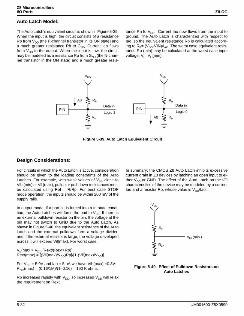
Z8 MicrocontrollersI/O Ports ZiLOG
Auto Latch Model:
The Auto Latch’s equivalent circuit is shown in Figure 5-39.When the input is high, the circuit consists of a resistanceRp from VDD (the P-channel transistor in its ON state) anda much greater resistance Rh to GND. Current Iao flowsfrom VDD to the output. When the input is low, the circuitmay be modeled as a resistance Rp from GND (the N-chan-nel transistor in the ON state) and a much greater resis-
tance Rh to VDD. Current Iao now flows from the input toground. The Auto Latch is characterized with respect toIao, so the equivalent resistance Rp is calculated accord-ing to RP= (VDD-VIN)/IAO. The worst case equivalent resis-tance Rp (min) may be calculated at the worst case inputvoltage, VI= VIH(min).
Design Considerations:
For circuits in which the Auto Latch is active, considerationshould be given to the loading constraints of the AutoLatches. For example, with weak values of VIN, close toVih (min) or Vil (max), pullup or pull-down resistances mustbe calculated using Ref = R/Rp. For best case STOPmode operation, the inputs should be within 200 mV of thesupply rails.
In output mode, if a port bit is forced into a tri-state condi-tion, the Auto Latches will force the pad to VDD. If there isan external pulldown resistor on the pin, the voltage at thepin may not switch to GND due to the Auto Latch. Asshown in Figure 5-40, the equivalent resistance of the AutoLatch and the external pulldown form a voltage divider,and if the external resistor is large, the voltage developedacross it will exceed Vil(max). For worst case:
VIL(max > VDD [Rext/(Rext+Rp)]Rext(max) = [(Vil(max)/VDD)Rp]/[1-(Vil(max)/VDD)]
For VDD = 5.0V and Iao = 5 uA we have Vih(max) =0.8V:REXT(max) = (0.16/1M)/(1–0.16) = 190 K ohms.
Rp increases rapidly with VDD, so increased VDD will relaxthe requirement on Rext.
In summary, the CMOS Z8 Auto Latch inhibits excessivecurrent drain in Z8 devices by latching an open input to ei-ther VDD or GND. The effect of the Auto Latch on the I/Ocharacteristics of the device may be modeled by a currentIao and a resistor Rp, whose value is VDD/Iao.
Figure 5-39. Auto Latch Equivalent Circuit
VDD
Data inPIN
Logic 1
A0
PIN
VDD
RP RH
RH RP
Data in
Logic 0
A0
Figure 5-40. Effect of Pulldown Resistors on Auto Latches
VLO
VIH (min.)
RP
REXT
5-32 UM001600-Z8X0599
USER’S MANUAL
CHAPTER 6COUNTER/TIMERS
6.1 INTRODUCTION
The Z8 MCU® provides up to two 8-bit counter/timers, T0and T1, each driven by its own 6-bit prescaler, PRE0 andPRE1 (Figure 6-1). Both counter/timers are independent ofthe processor instruction sequence, that relieves softwarefrom time-critical operations such as interval timing orevent counting. Some MCUs offer clock scaling using theSMR register. See the device product specification forclock available options. The following description is typical.
Each counter/timer operates in either Single-Pass or Con-tinuous mode. At the end-of-count, counting either stops orthe initial value is reloaded and counting continues. Undersoftware control, new values are loaded immediately orwhen the end-of-count is reached. Software also controlsthe counting mode, how a counter/timer is started orstopped, and its use of I/O lines. Both the counter andprescaler registers can be altered while the counter/timeris running.
Figure 6-1. Counter/Timer Block Diagram
÷2
OSC
D1 (SMR)
÷16
D0 (SMR)
Clock
÷4
Logic
InternalClock
External Clock
Internal ClockGated ClockTriggered Clock
TIN P31
÷4
6-BitDownCounter
8-BitDownCounter
PRE1Initial ValueRegister
T1Initial ValueRegister
T1Current ValueRegister
Write ReadWrite
Write ReadWrite
6-BitDownCounter
8-BitDownCounter
PRE0Initial ValueRegister
T0Initial ValueRegister
T0Current ValueRegister
÷2
Internal Data Bus
Internal Data Bus
TOUT
IRQ4
P36
IRQ5
UM001600-Z8X0599 6-1
Z8 MicrocontrollersCounter/Timers ZiLOG
Counter/timers 0 and 1 are driven by a timer clock gener-ated by dividing the internal clock by four. The divide-by-four stage, the 6-bit prescaler, and the 8-bit counter/timerform a synchronous 16-bit divide chain. Counter/timer 1can also be driven by a external input (TIN) using P31. Port3 line P36 can serve as a timer output (TOUT) throughwhich T0, T1, or the internal clock can be output. The timeroutput will toggle at the end-of-count.
The counter/timer, prescaler, and associated mode regis-ters are mapped into the register file as shown in Figure 6-2. This allows the software to treat the counter/timers asgeneral-purpose registers, and eliminates the need forspecial instructions.
6.2 PRESCALERS AND COUNTER/TIMERS
The prescalers, PRE0 (F5H) and PRE1 (F3H), each con-sist of an 8-bit register and a 6-bit down-counter as shownin Figure 6-1. The prescaler registers are write-only regis-ters. Reading the prescalers returns the value FFH. Fig-ures 6-3 and 6-4 show the prescaler registers.
The six most significant bits (D2-D7) of PRE0 or PRE1hold the prescalers count modulo, a value from 1 to 64decimal. The prescaler registers also contain control bitsthat specify T0 and T1 counting modes. These bits also in-dicate whether the clock source for T1 is internal or exter-nal. These control bits will be discussed in detail through-out this chapter.
The counter/timer registers, T0 (F4H) and T1 (F2H), eachconsist of an 8-bit down-counter, a write-only register thatholds the initial count value, and a read-only register thatholds the current count value (Figure 6-1). The initial valuecan range from 1 to 256 decimal (01H,02H,..,00H). Figure6-5 illustrates the counter/timer registers.
Figure 6-2. Counter/Timer Register Map
HEX Identifiers
T0 Prescaler
F7
Timer/Counter0
Port 3 Mode
T1 Prescaler
Time/Counter1
Timer Mode
F5
F4
F3
F2
F1
DEC
247
245
244
243
242
241
Figure 6-3. Prescaler 0 Register
Figure 6-4. Prescaler 1 Register
Figure 6-5. Counter / Timer 0 and 1 Registers
D7 D6 D5 D4 D3 D2 D1 D0
(%F5; Write-Only)
1 = T0 Modulo-n
Count Mode 0 = T0 Single Pass
Prescaler 0 RegisterR245 PRE0
01-00 HEX)
Prescaler Modulo (Range: 1-64 Decimal
Reserved (Must be 0)
U U U U U U 0 0
(%F3; Write-Only)
1 = T1 Modulo-n
Count Mode 0 = T1 Single Pass
Prescaler 1 RegisterR243 PRE1
01-00 HEX)
Prescaler Modulo (Range: 1-64 Decimal
Clock Source
0 = T1 External (TIN) 1 = T1 Internal
D7 D6 D5 D4 D3 D2 D1 D0
(%F4; Write/Read Only)
current value when read
Initial value when written (Range 1-256 decimal, 01-00 HEX)
Counter/Timer 0 RegisterR244 T0
(%F2; Write/Read Only)Counter/Timer 1 RegisterR242 T1
6-2 UM001600-Z8X0599
Z8 MicrocontrollersZiLOG Counter/Timers
6.3 COUNTER/TIMER OPERATION
Under software control, counter/timers are started andstopped via the Timer Mode Register (TMR,F1H) bits D0-D3 (Figure 6-6). Each counter/timer is associated with aLoad bit and an Enable Count bit.
6.3.1 Load and Enable Count BitsSetting the Load bit (D0 for T0 and D2 for T1) transfers theinitial value in the prescaler and the counter/timer registersinto their respective down-counters. The next internalclock resets bits D0 and D2 to 0, readying the Load bit forthe next load operation. New values may be loaded intothe down-counters at any time. If the counter/timer is run-ning, it continues to do so and starts the count over withthe new value. Therefore, the Load bit actually functions asa software re-trigger.
The counter timers remain at rest as long as the EnableCount bits are 0. To enable counting, the Enable Count bit(D1 for T0 and D3 for T1) must be set to 1. Counting actu-ally starts when the Enable Count bit is written by an in-struction. The first decrement occurs four internal clock pe-riods after the Enable Count bit has been set. If T1 isconfigured to use an external clock, the first decrement be-gins on the next clock period. The Load and Enable Countbits can be set at the same time. For example, using theinstruction:
OR TMR,#03H
sets both D0 and D1 of the TMR. This loads the initial val-ues of PRE0 and T0 into their respective counters andstarts the count after the M2T2 machine state after the op-erand is fetched (Figure 6-7).
Figure 6-6. Timer Mode Register
D3 D2 D1 D0
(% F1; Read/Write)
0 = Disable T0 Count
0 = No Function 1 = Load T0
Timer Mode RegisterR241 TMR
1 = Enable T0 Count
0 = No Function 1 = Load T1
0 = Disable T1 Count 1 = Enable T1 Count
Figure 6-7. Starting The Count
D0
(% F5; Write-Only)
Count Mode
Prescaler 0 RegisterR245 PRE0
(% F3; Write-Only)Prescaler 1 RegisterR243 PRE1
0 = T1 Single Pass 1 = T1 Modulo-n
Figure 6-8. Counting Modes
T1 T2 T3 T1 T2 T3 T1 T2 T3 T1 T2 T3
TMR is Written, Counter/Timer
First Decrement Occurs Four Clock Periods Later
is Loaded
#03H is Fetched
M3 M1 M2 Mn
UM001600-Z8X0599 6-3
Z8 MicrocontrollersCounter/Timers ZiLOG
6.3.2 Prescaler OperationsDuring counting, the programmed clock source drives the6-bit Prescaler Counter. The counter is counted down fromthe value specified by bits of the corresponding PrescalerRegister, PRE0 (bit 7 to bit 2) or PRE1 (bit 7 to bit 2). (Fig-ures 6-3, 6-4). When the Prescaler Counter reaches itsend-of-count, the initial value is reloaded and countingcontinues. The prescaler never actually reaches 0. For ex-ample, if the prescaler is set to divide-by-three, the countsequence is:
Each time the prescaler reaches its end of count a carry isgenerated, that allows the Counter/Timer to decrement byone on the next timer clock input. When the Counter/Timerand the prescaler both reach the end-of-count, an interruptrequest is generated (IRQ4 for T0, IRQ5 for T1). Depend-ing on the counting mode selected, the Counter/Timer willeither come to rest with its value at 00H (Single-PassMode) or the initial value will be automatically reloadedand counting will continue (Continuous Mode). The count-ing modes are controlled by bit 0 of PRE0 and bit 0 ofPRE1. (Figure 6-8). A 0, written to this bit configures thecounter for Single-pass counting mode, while a 1 written tothis bit configures the counter for Continuous mode.
The Counter/Timer can be stopped at any time by settingthe Enable Count bit to 0, and restarted by setting it backto 1. The Counter/Timer will continue its count value at thetime it was stopped. The current value in the Counter/Tim-er can be read at any time without affecting the countingoperation.
Note: The prescaler registers are write-only and cannotbe read.
New initial values can be written to the prescaler or theCounter/Timer registers at any time. These values will betransferred to their respective down counters on the nextload operation. If the Counter/Timer mode is continuous,the next load occurs on the timer clock following an end-of-count. New initial values should be written before the de-sired load operation, since the prescalers always effective-ly operate in Continuous count mode.
The time interval (i) until end-of-count, is given by theequation:
The internal clock frequency defaults to the external clocksource (XTAL, ceramic resonator, and others) divided by2. Some Z8 microcontrollers allow this divisor to bechanged via the Stop-Mode Recovery register. See theproduct data sheet for available clock divisor options.
Note that t is equal to eight divided-by-XTAL frequency ofthe external clock source for T1 (external clock modeonly).
p = the prescaler value (1 – 63) for T0 and T1.
The minimum prescaler count of 1 is achieved by loading000001xx. The maximum prescaler count of 63 isachieved by loading 111111xx.
v = the Counter/Timer value (1-256)
Minimum duration is achieved by loading 01H (1 prescaleroutput count), maximum duration is achieved by loading00H (256 prescaler outputs counts).
The prescaler and counter/timer are true divide-by-ncounters.
3–2–1–3–2–1–3–2–1–3...
i = t X p X v in which:t = four times the internal clock period.
6-4 UM001600-Z8X0599
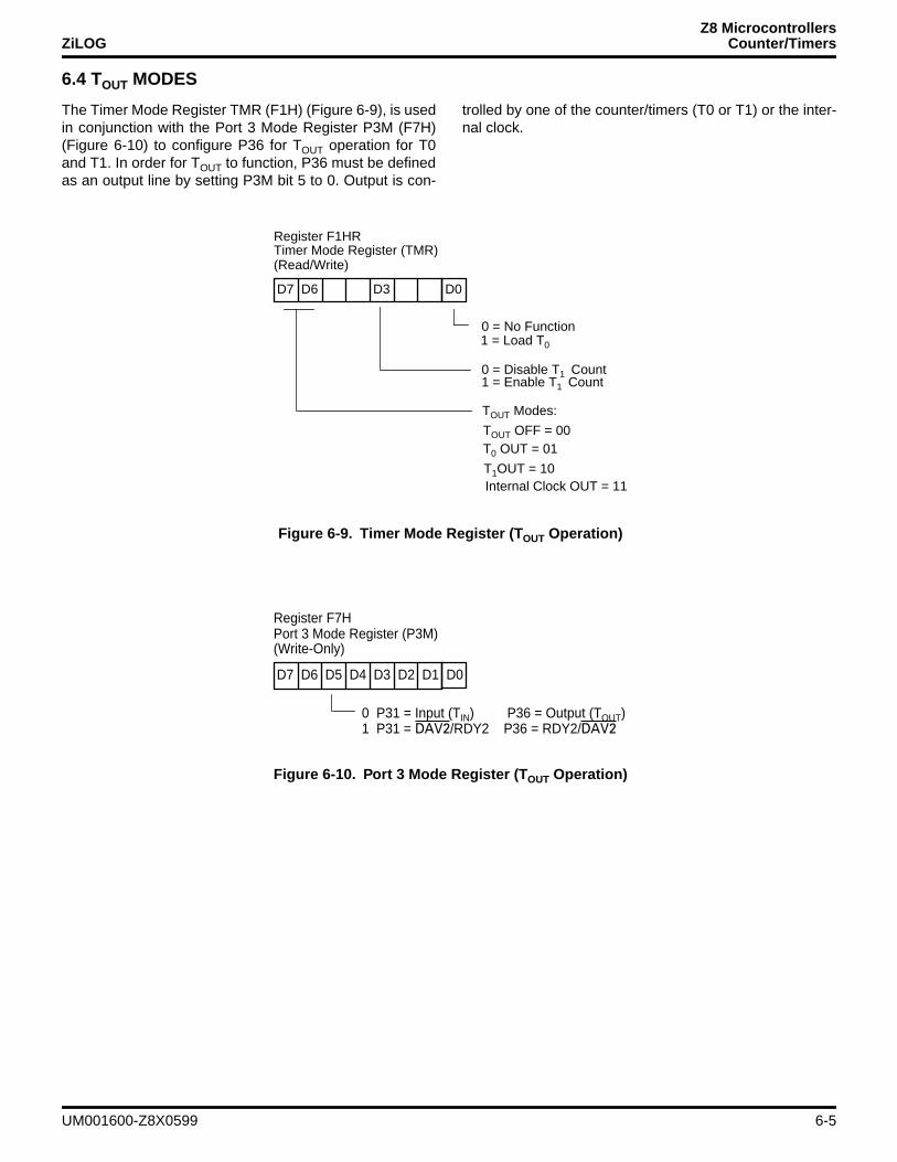
Z8 MicrocontrollersZiLOG Counter/Timers
6.4 TOUT MODES
The Timer Mode Register TMR (F1H) (Figure 6-9), is usedin conjunction with the Port 3 Mode Register P3M (F7H)(Figure 6-10) to configure P36 for TOUT operation for T0and T1. In order for TOUT to function, P36 must be definedas an output line by setting P3M bit 5 to 0. Output is con-
trolled by one of the counter/timers (T0 or T1) or the inter-nal clock.
Figure 6-9. Timer Mode Register (T OUT Operation)
D7 D6 D3 D0
(Read/Write)
0 = No Function 1 = Load T0
Timer Mode Register (TMR)Register F1HR
TOUT Modes:
0 = Disable T1 Count 1 = Enable T1 Count
TOUT OFF = 00 T0 OUT = 01
T1OUT = 10 Internal Clock OUT = 11
Figure 6-10. Port 3 Mode Register (T OUT Operation)
D7 D6 D5 D4 D3 D2 D1 D0
(Write-Only)Port 3 Mode Register (P3M)Register F7H
0 P31 = Input (TIN) P36 = Output (TOUT) 1 P31 = DAV2/RDY2 P36 = RDY2/DAV2
UM001600-Z8X0599 6-5
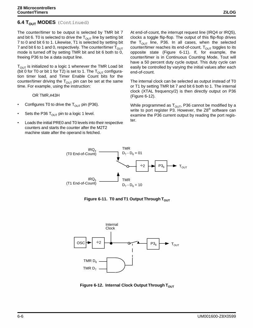
Z8 MicrocontrollersCounter/Timers ZiLOG
6.4 TOUT MODES (Continued)
The counter/timer to be output is selected by TMR bit 7and bit 6. T0 is selected to drive the TOUT line by setting bit7 to 0 and bit 6 to 1. Likewise, T1 is selected by setting bit7 and bit 6 to 1 and 0, respectively. The counter/timer TOUTmode is turned off by setting TMR bit and bit 6 both to 0,freeing P36 to be a data output line.
TOUT is initialized to a logic 1 whenever the TMR Load bit(bit 0 for T0 or bit 1 for T2) is set to 1. The TOUT configura-tion timer load, and Timer Enable Count bits for thecounter/timer driving the TOUT pin can be set at the sametime. For example, using the instruction:
OR TMR,#43H
• Configures T0 to drive the TOUT pin (P36).
• Sets the P36 TOUT pin to a logic 1 level.
• Loads the initial PRE0 and T0 levels into their respectivecounters and starts the counter after the M2T2machine state after the operand is fetched.
At end-of-count, the interrupt request line (IRQ4 or IRQ5),clocks a toggle flip-flop. The output of this flip-flop drivesthe TOUT line, P36. In all cases, when the selectedcounter/timer reaches its end-of-count, TOUT toggles to itsopposite state (Figure 6-11). If, for example, thecounter/timer is in Continuous Counting Mode, Tout willhave a 50 percent duty cycle output. This duty cycle caneasily be controlled by varying the initial values after eachend-of-count.
The internal clock can be selected as output instead of T0or T1 by setting TMR bit 7 and bit 6 both to 1. The internalclock (XTAL frequency/2) is then directly output on P36(Figure 6-12).
While programmed as TOUT, P36 cannot be modified by awrite to port register P3. However, the Z8® software canexamine the P36 current output by reading the port regis-ter.
Figure 6-11. T0 and T1 Output Through T OUT
÷2 P36 TOUT
TMRD7 - D6 = 01
IRQ4(T0 End-of-Count)
IRQ5(T1 End-of-Count)
TMRD7 - D6 = 10
Figure 6-12. Internal Clock Output Through T OUT
OSC ÷2 P36 TOUT
Internal
TMR D6
Clock
TMR D7
6-6 UM001600-Z8X0599
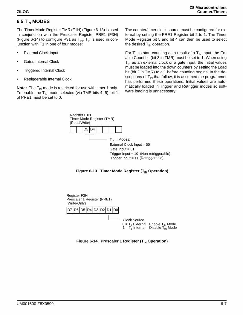
Z8 MicrocontrollersZiLOG Counter/Timers
6.5 TIN MODES
The Timer Mode Register TMR (F1H) (Figure 6-13) is usedin conjunction with the Prescaler Register PRE1 (F3H)(Figure 6-14) to configure P31 as TIN. TIN is used in con-junction with T1 in one of four modes:
• External Clock Input
• Gated Internal Clock
• Triggered Internal Clock
• Retriggerable Internal Clock
Note: The TIN mode is restricted for use with timer 1 only.To enable the TIN mode selected (via TMR bits 4- 5), bit 1of PRE1 must be set to 0.
The counter/timer clock source must be configured for ex-ternal by setting the PRE1 Register bit 2 to 1. The TimerMode Register bit 5 and bit 4 can then be used to selectthe desired TIN operation.
For T1 to start counting as a result of a TIN input, the En-able Count bit (bit 3 in TMR) must be set to 1. When usingTIN as an external clock or a gate input, the initial valuesmust be loaded into the down counters by setting the Loadbit (bit 2 in TMR) to a 1 before counting begins. In the de-scriptions of TIN that follow, it is assumed the programmerhas performed these operations. Initial values are auto-matically loaded in Trigger and Retrigger modes so soft-ware loading is unnecessary.
Figure 6-13. Timer Mode Register (T IN Operation)
D5 D4
(Read/Write)
Timer Mode Register (TMR)Register F1H
(Retriggerable)
(Non-retriggerable) Trigger Input = 10
TIN = Modes: External Clock Input = 00 Gate Input = 01
Trigger Input = 11
Figure 6-14. Prescaler 1 Register (T IN Operation)
D7 D6 D5 D4 D3 D2 D1 D0
(Write-Only)
1 = T1 Internal Disable TIN Mode
Clock Source 0 = T1 External Enable TIN Mode
Prescaler 1 Register (PRE1)Register F3H
UM001600-Z8X0599 6-7
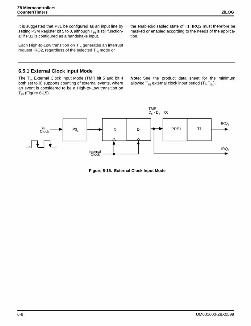
Z8 MicrocontrollersCounter/Timers ZiLOG
It is suggested that P31 be configured as an input line bysetting P3M Register bit 5 to 0, although TIN is still function-al if P31 is configured as a handshake input.
Each High-to-Low transition on TIN generates an interruptrequest IRQ2, regardless of the selected TIN mode or
the enabled/disabled state of T1. IRQ2 must therefore bemasked or enabled according to the needs of the applica-tion.
6.5.1 External Clock Input ModeThe TIN External Clock Input Mode (TMR bit 5 and bit 4both set to 0) supports counting of external events, wherean event is considered to be a High-to-Low transition onTIN (Figure 6-15).
Note: See the product data sheet for the minimumallowed TIN external clock input period (TP TIN).
Figure 6-15. External Clock Input Mode
DP31
Internal IRQ2
TMR
TINClock D PRE1 T1
IRQ5
D5 - D4 = 00
Clock
6-8 UM001600-Z8X0599
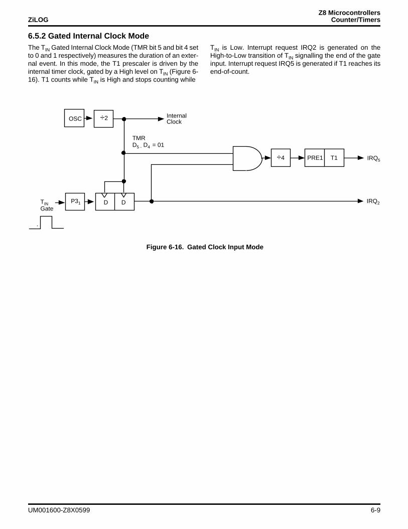
Z8 MicrocontrollersZiLOG Counter/Timers
6.5.2 Gated Internal Clock ModeThe TIN Gated Internal Clock Mode (TMR bit 5 and bit 4 setto 0 and 1 respectively) measures the duration of an exter-nal event. In this mode, the T1 prescaler is driven by theinternal timer clock, gated by a High level on TIN (Figure 6-16). T1 counts while TIN is High and stops counting while
TIN is Low. Interrupt request IRQ2 is generated on theHigh-to-Low transition of TIN signalling the end of the gateinput. Interrupt request IRQ5 is generated if T1 reaches itsend-of-count.
Figure 6-16. Gated Clock Input Mode
OSC ÷2
÷4
D D
PRE1
P31
T1
IRQ2TIN
IRQ5
Gate
Internal
TMRD5 - D4 = 01
Clock
UM001600-Z8X0599 6-9
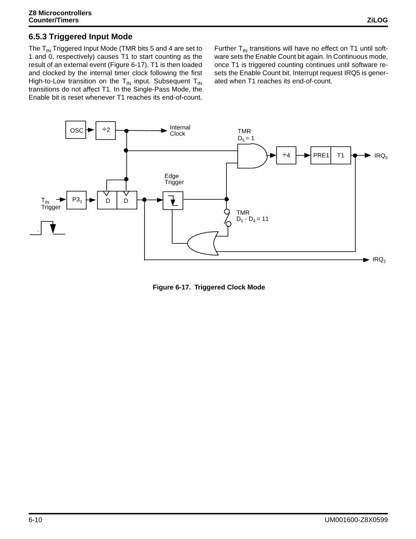
Z8 MicrocontrollersCounter/Timers ZiLOG
6.5.3 Triggered Input ModeThe TIN Triggered Input Mode (TMR bits 5 and 4 are set to1 and 0, respectively) causes T1 to start counting as theresult of an external event (Figure 6-17). T1 is then loadedand clocked by the internal timer clock following the firstHigh-to-Low transition on the TIN input. Subsequent TINtransitions do not affect T1. In the Single-Pass Mode, theEnable bit is reset whenever T1 reaches its end-of-count.
Further TIN transitions will have no effect on T1 until soft-ware sets the Enable Count bit again. In Continuous mode,once T1 is triggered counting continues until software re-sets the Enable Count bit. Interrupt request IRQ5 is gener-ated when T1 reaches its end-of-count.
Figure 6-17. Triggered Clock Mode
OSC ÷2
÷4
D D
PRE1
TMR
P31
T1
IRQ2
TIN
IRQ5
Trigger
D5 - D4 = 11
InternalTMRD5 = 1
Clock
EdgeTrigger
6-10 UM001600-Z8X0599
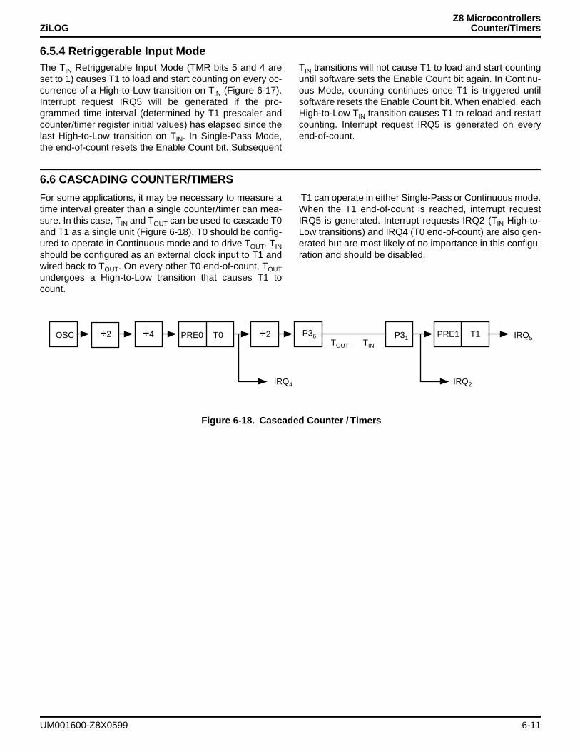
Z8 MicrocontrollersZiLOG Counter/Timers
6.5.4 Retriggerable Input ModeThe TIN Retriggerable Input Mode (TMR bits 5 and 4 areset to 1) causes T1 to load and start counting on every oc-currence of a High-to-Low transition on TIN (Figure 6-17).Interrupt request IRQ5 will be generated if the pro-grammed time interval (determined by T1 prescaler andcounter/timer register initial values) has elapsed since thelast High-to-Low transition on TIN. In Single-Pass Mode,the end-of-count resets the Enable Count bit. Subsequent
TIN transitions will not cause T1 to load and start countinguntil software sets the Enable Count bit again. In Continu-ous Mode, counting continues once T1 is triggered untilsoftware resets the Enable Count bit. When enabled, eachHigh-to-Low TIN transition causes T1 to reload and restartcounting. Interrupt request IRQ5 is generated on everyend-of-count.
6.6 CASCADING COUNTER/TIMERS
For some applications, it may be necessary to measure atime interval greater than a single counter/timer can mea-sure. In this case, TIN and TOUT can be used to cascade T0and T1 as a single unit (Figure 6-18). T0 should be config-ured to operate in Continuous mode and to drive TOUT. TINshould be configured as an external clock input to T1 andwired back to TOUT. On every other T0 end-of-count, TOUTundergoes a High-to-Low transition that causes T1 tocount.
T1 can operate in either Single-Pass or Continuous mode.When the T1 end-of-count is reached, interrupt requestIRQ5 is generated. Interrupt requests IRQ2 (TIN High-to-Low transitions) and IRQ4 (T0 end-of-count) are also gen-erated but are most likely of no importance in this configu-ration and should be disabled.
Figure 6-18. Cascaded Counter / Timers
OSC ÷2 ÷4 PRE0 T0 ÷2 PRE1
IRQ2
P31P36 T1
IRQ4
TOUT TIN
IRQ5
UM001600-Z8X0599 6-11
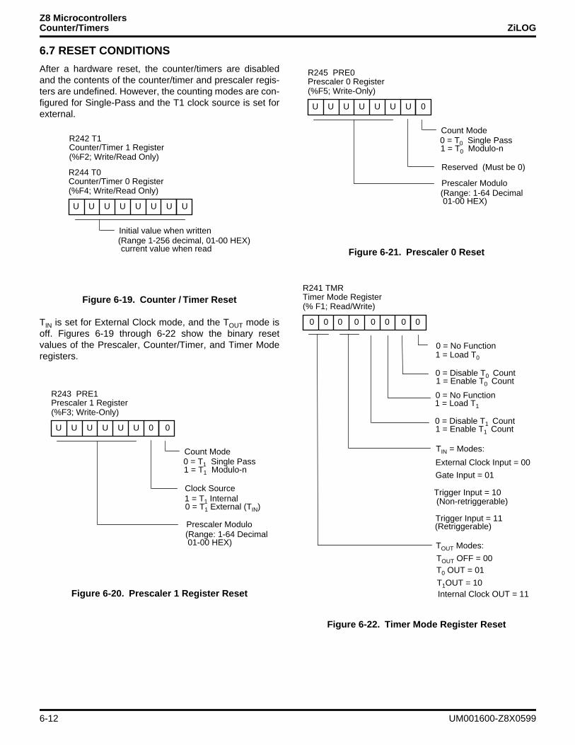
Z8 MicrocontrollersCounter/Timers ZiLOG
6.7 RESET CONDITIONS
After a hardware reset, the counter/timers are disabledand the contents of the counter/timer and prescaler regis-ters are undefined. However, the counting modes are con-figured for Single-Pass and the T1 clock source is set forexternal.
TIN is set for External Clock mode, and the TOUT mode isoff. Figures 6-19 through 6-22 show the binary resetvalues of the Prescaler, Counter/Timer, and Timer Moderegisters.
Figure 6-19. Counter / Timer Reset
Figure 6-20. Prescaler 1 Register Reset
U U U U U U U U
(%F4; Write/Read Only)
current value when read
Initial value when written (Range 1-256 decimal, 01-00 HEX)
Counter/Timer 0 RegisterR244 T0
(%F2; Write/Read Only)Counter/Timer 1 RegisterR242 T1
U U U U U U 0 0
(%F3; Write-Only)
1 = T1 Modulo-n
Count Mode 0 = T1 Single Pass
Prescaler 1 RegisterR243 PRE1
01-00 HEX)
Prescaler Modulo (Range: 1-64 Decimal
Clock Source
0 = T1 External (TIN) 1 = T1 Internal
Figure 6-21. Prescaler 0 Reset
Figure 6-22. Timer Mode Register Reset
U U U U U U U 0
(%F5; Write-Only)
1 = T0 Modulo-n
Count Mode 0 = T0 Single Pass
Prescaler 0 RegisterR245 PRE0
01-00 HEX)
Prescaler Modulo (Range: 1-64 Decimal
Reserved (Must be 0)
0 0 0 0 0 0 0 0
(% F1; Read/Write)
0 = Disable T0 Count
0 = No Function 1 = Load T0
Timer Mode RegisterR241 TMR
1 = Enable T0 Count
(Retriggerable)
TOUT Modes:
(Non-retriggerable) Trigger Input = 10
TIN = Modes:
External Clock Input = 00
Gate Input = 01
0 = No Function 1 = Load T1
0 = Disable T1 Count 1 = Enable T1 Count
TOUT OFF = 00 T0 OUT = 01
T1OUT = 10 Internal Clock OUT = 11
Trigger Input = 11
6-12 UM001600-Z8X0599
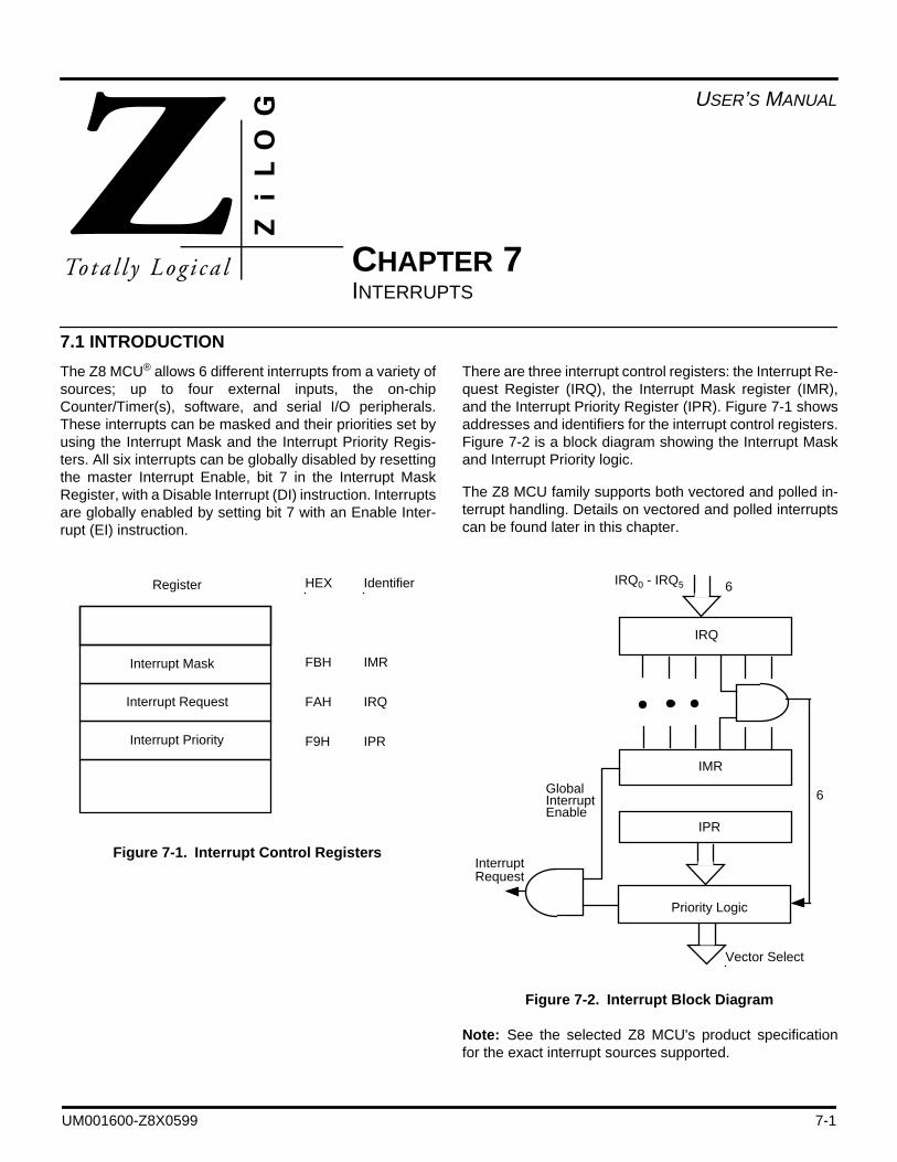
USER’S MANUAL
CHAPTER 7INTERRUPTS
7.1 INTRODUCTION
The Z8 MCU® allows 6 different interrupts from a variety ofsources; up to four external inputs, the on-chipCounter/Timer(s), software, and serial I/O peripherals.These interrupts can be masked and their priorities set byusing the Interrupt Mask and the Interrupt Priority Regis-ters. All six interrupts can be globally disabled by resettingthe master Interrupt Enable, bit 7 in the Interrupt MaskRegister, with a Disable Interrupt (DI) instruction. Interruptsare globally enabled by setting bit 7 with an Enable Inter-rupt (EI) instruction.
There are three interrupt control registers: the Interrupt Re-quest Register (IRQ), the Interrupt Mask register (IMR),and the Interrupt Priority Register (IPR). Figure 7-1 showsaddresses and identifiers for the interrupt control registers.Figure 7-2 is a block diagram showing the Interrupt Maskand Interrupt Priority logic.
The Z8 MCU family supports both vectored and polled in-terrupt handling. Details on vectored and polled interruptscan be found later in this chapter.
Note: See the selected Z8 MCU's product specificationfor the exact interrupt sources supported.
Figure 7-1. Interrupt Control Registers
Register HEX
Interrupt Mask
Interrupt Request
Interrupt Priority
Identifier
FBH
FAH
F9H
IMR
IRQ
IPR
Figure 7-2. Interrupt Block Diagram
IRQ
IRQ0 - IRQ5
Vector Select
InterruptRequest
IMR
IPR
Priority Logic
6GlobalInterruptEnable
6
UM001600-Z8X0599 7-1
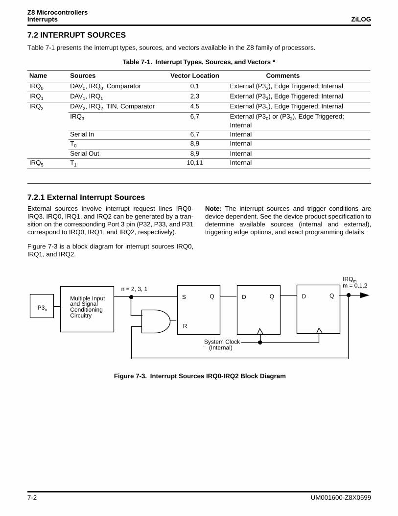
Z8 MicrocontrollersInterrupts ZiLOG
7.2 INTERRUPT SOURCES
Table 7-1 presents the interrupt types, sources, and vectors available in the Z8 family of processors.
7.2.1 External Interrupt SourcesExternal sources involve interrupt request lines IRQ0-IRQ3. IRQ0, IRQ1, and IRQ2 can be generated by a tran-sition on the corresponding Port 3 pin (P32, P33, and P31correspond to IRQ0, IRQ1, and IRQ2, respectively).
Figure 7-3 is a block diagram for interrupt sources IRQ0,IRQ1, and IRQ2.
Note: The interrupt sources and trigger conditions aredevice dependent. See the device product specification todetermine available sources (internal and external),triggering edge options, and exact programming details.
Table 7-1. Interrupt Types, Sources, and Vectors *
Name Sources Vector Location Comments
IRQ0 DAV0, IRQ0, Comparator 0,1 External (P32), Edge Triggered; Internal
IRQ1 DAV1, IRQ1 2,3 External (P33), Edge Triggered; Internal
IRQ2 DAV2, IRQ2, TIN, Comparator 4,5 External (P31), Edge Triggered; Internal
IRQ3 6,7 External (P30) or (P32), Edge Triggered; Internal
Serial In 6,7 InternalT0 8,9 Internal
Serial Out 8,9 InternalIRQ5 T1 10,11 Internal
Figure 7-3. Interrupt Sources IRQ0-IRQ2 Block Diagram
P3n
IRQm
System Clock
Multiple Input
n = 2, 3, 1
and SignalQS
R
ConditioningCircuitry
m = 0,1,2
(Internal)
QD QD
7-2 UM001600-Z8X0599
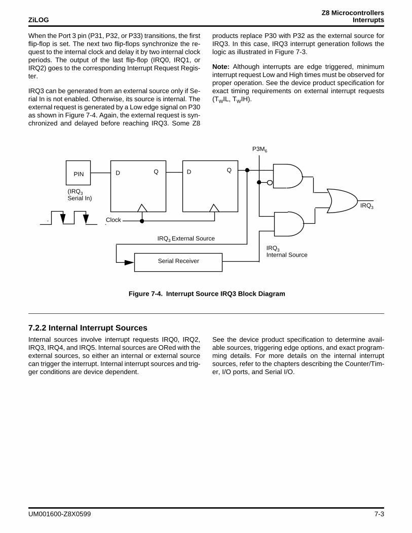
Z8 MicrocontrollersZiLOG Interrupts
When the Port 3 pin (P31, P32, or P33) transitions, the firstflip-flop is set. The next two flip-flops synchronize the re-quest to the internal clock and delay it by two internal clockperiods. The output of the last flip-flop (IRQ0, IRQ1, orIRQ2) goes to the corresponding Interrupt Request Regis-ter.
IRQ3 can be generated from an external source only if Se-rial In is not enabled. Otherwise, its source is internal. Theexternal request is generated by a Low edge signal on P30as shown in Figure 7-4. Again, the external request is syn-chronized and delayed before reaching IRQ3. Some Z8
products replace P30 with P32 as the external source forIRQ3. In this case, IRQ3 interrupt generation follows thelogic as illustrated in Figure 7-3.
Note: Although interrupts are edge triggered, minimuminterrupt request Low and High times must be observed forproper operation. See the device product specification forexact timing requirements on external interrupt requests(TWIL, TWIH).
7.2.2 Internal Interrupt SourcesInternal sources involve interrupt requests IRQ0, IRQ2,IRQ3, IRQ4, and IRQ5. Internal sources are ORed with theexternal sources, so either an internal or external sourcecan trigger the interrupt. Internal interrupt sources and trig-ger conditions are device dependent.
See the device product specification to determine avail-able sources, triggering edge options, and exact program-ming details. For more details on the internal interruptsources, refer to the chapters describing the Counter/Tim-er, I/O ports, and Serial I/O.
Figure 7-4. Interrupt Source IRQ3 Block Diagram
QPIN D
Serial Receiver
P3M6
IRQ3
Clock
IRQ3
IRQ3 External Source
(IRQ3Serial In)
Internal Source
D Q
UM001600-Z8X0599 7-3
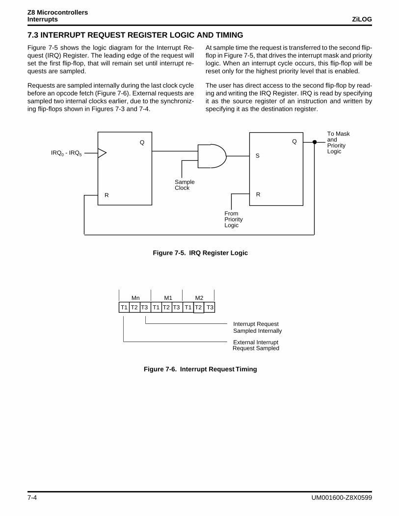
Z8 MicrocontrollersInterrupts ZiLOG
7.3 INTERRUPT REQUEST REGISTER LOGIC AND TIMING
Figure 7-5 shows the logic diagram for the Interrupt Re-quest (IRQ) Register. The leading edge of the request willset the first flip-flop, that will remain set until interrupt re-quests are sampled.
Requests are sampled internally during the last clock cyclebefore an opcode fetch (Figure 7-6). External requests aresampled two internal clocks earlier, due to the synchroniz-ing flip-flops shown in Figures 7-3 and 7-4.
At sample time the request is transferred to the second flip-flop in Figure 7-5, that drives the interrupt mask and prioritylogic. When an interrupt cycle occurs, this flip-flop will bereset only for the highest priority level that is enabled.
The user has direct access to the second flip-flop by read-ing and writing the IRQ Register. IRQ is read by specifyingit as the source register of an instruction and written byspecifying it as the destination register.
Figure 7-5. IRQ Register Logic
Q
S
From
To Mask
IRQ0 - IRQ5
R
Q
R
PriorityLogic
and PriorityLogic
SampleClock
Figure 7-6. Interrupt Request Timing
T1 T2 T3 T1 T2 T3 T1 T2 T3
External Interrupt
Interrupt Request Sampled Internally
Request Sampled
Mn M1 M2
7-4 UM001600-Z8X0599
Z8 MicrocontrollersZiLOG Interrupts
7.4 INTERRUPT INITIALIZATION
After reset, all interrupts are disabled and must be initial-ized before vectored or polled interrupt processing can be-gin. The Interrupt Priority Register (IPR), Interrupt MaskRegister (IMR), and Interrupt Request Register (IRQ) mustbe initialized, in that order, to start the interrupt process.
7.4.1 Interrupt Priority Register (IPR) Initial-izationIPR (Figure 7-7) is a write-only register that sets prioritiesfor the vectored interrupts in order to resolve simultaneousinterrupt requests. (There are 48 sequence possibilities for
interrupts.) The six interrupt levels IRQ0-IRQ5 are dividedinto three groups of two interrupt requests each. Onegroup contains IRQ3 and IRQ5. The second group con-tains IRQ0 and IRQ2, while the third group contains IRQ1and IRQ4.
Priorities can be set both within and between groups asshown in Tables 7-2 and 7-3. Bits 1, 2, and 5 define the pri-ority of the individual members within the three groups.Bits 0, 3, and 4 are encoded to define six priority orders be-tween the three groups. Bits 6 and 7 are reserved.
Figure 7-7. Interrupt Priority Register
D7 D6 D5 D4 D3 D2 D1 D0
(Write-Only)
Interrupt Priority Register (IPR)Register F9H
Interrupt Group Priority Bits Priority
000 Reserved 001 C > A > B
010 A > B > C 011 A > C > B
100 B > C > A 101 C > B > A
110 B > A > C 111 Reserved
0 = IRQ1 > IRQ4 1 = IRQ4 > IRQ1 Group C (IRQ1 and IRQ4 Priority)
Reserved (Must be 0)
0 = IRQ2 > IRQ0 1 = IRQ0 > IRQ2 Group B (IRQ0 and IRQ2 Priority)
0 = IRQ5 > IRQ3 1 = IRQ3 > IRQ5 Group A (IRQ3 and IRQ5 Priority)
Table 7-2. Interrupt Priority
PriorityGroup Bit Value Highest Lowest
C Bit 1 0 IRQ1 IRQ41 IRQ4 IRQ1
B Bit 2 0 IRQ2 IRQ01 IRQ0 IRQ2
A Bit 5 0 IRQ5 IRQ31 IRQ3 IRQ5
Table 7-3. Interrupt Group Priority
Bit Pattern Group PriorityBit 4 Bit 3 Bit 0 High Medium Low
0 0 0 Not Used0 0 1 C A B0 1 0 A B C0 1 1 A C B1 0 0 B C A1 0 1 C B A1 1 0 B A C1 1 1 Not Used
UM001600-Z8X0599 7-5
Z8 MicrocontrollersInterrupts ZiLOG
7.4 INTERRUPT INITIALIZATION (Continued)
7.4.2 Interrupt Mask Register (IMR) InitializationIMR individually or globally enables or disables the six in-terrupt requests (Figure 7-8). When bit 0 to bit 5 are set to1, the corresponding interrupt requests are enabled. Bit 7is the master enable and must be set before any of the in-dividual interrupt requests can be recognized. Resettingbit 7 globally disables all the interrupt requests. Bit 7 is setand reset by the EI and DI instructions. It is automaticallyreset during an interrupt service routine and set followingthe execution of an Interrupt Return (IRET) instruction.
Note: Bit 7 must be reset by the DI instruction before thecontents of the Interrupt Mask Register or the InterruptPriority Register are changed except:
• Immediately after a hardware reset.
• Immediately after executing an interrupt service routineand before IMR bit 7 has been set by any instruction.
Note: The RAM Protect option is selected at ROM masksubmission time or at EPROM program time. If notselected or not an available option, this bit is reserved andmust be 0.
Figure 7-8. Interrupt Mask Register
D7 D6 D5 D4 D3 D2 D1 D0
(Read/Write)
Interrupt Request Register (IMR)Register FBH
0 = Disables IRQ0 1 = Enables IRQ0
0 = Disables IRQ1 1 = Enables IRQ1
0 = Disables IRQ2 1 = Enables IRQ2
0 = Disables IRQ3 1 = Enables IRQ3
0 = Disables IRQ4 1 = Enables IRQ4
0 = Disables IRQ5 1 = Enables IRQ5
0 = Disables RAM Protect 1 = Enables RAM Protect
0 = Disables Interrupt 1 = Enables Interrupt
7-6 UM001600-Z8X0599
Z8 MicrocontrollersZiLOG Interrupts
7.4.3 Interrupt Request (IRQ) Register InitializationIRQ (Figure 7-9) is a read/write register that stores the in-terrupt requests for both vectored and polled interrupts.When an interrupt is made on any of the six, the corre-sponding bit position in the register is set to 1. Bit 0 to bit 5are assigned to interrupt requests IRQ0 to IRQ5, respec-tively.
Whenever Power-On Reset (POR) is executed, the IRQresister is reset to 00H and disabled. Before the IRQ reg-ister will accept requests, it must be enabled by executingan ENABLE INTERRUPTS (EI) instruction.
Note: Setting the Global Interrupt Enable bit in theInterrupt Mask Register (IMR, bit 7) will not enable theIRQ. Execution of the EI instruction is required (Figure 7-10).
For polled processing, IRQ must still be initialized by an EIinstruction.
To properly initialize the IRQ register, the following code isprovided:
Note: IRQ is always cleared to 00Hex and is read onlyuntil the 1st EI instruction which enables the IRQ to beread/write.
CLR IMR //make sure disabled vectored interruptsEI //enable IRQ register otherwise read
only.//not needed if interrupts were previously enabled.
DI //disable interrupt heading.
Figure 7-9. Interrupt Request Register
D7 D6 D5 D4 D3 D2 D1 D0
(Read/Write)
Reserved /Int Edge Select
Interrupt Request Register (IRQ)Register FAH
0 = IRQ0 RESET 1 = IRQ0 SET
0 = IRQ1 RESET 1 = IRQ1 SET
0 = IRQ2 RESET 1 = IRQ2 SET
0 = IRQ3 RESET 1 = IRQ3 SET
0 = IRQ4 RESET 1 = IRQ4 SET
0 = IRQ5 RESET 1 = IRQ5 SET
UM001600-Z8X0599 7-7
Z8 MicrocontrollersInterrupts ZiLOG
7.4 INTERRUPT INITIALIZATION (Continued)
IMR is cleared before the IRQ enabling sequence to insureno unexpected interrupts occur when EI is executed. Thiscode sequence should be executed prior to programmingthe application required values for IPR and IMR.
Note: IRQ bits 6 and 7 are device dependent. Whenreserved, the bits are not used and will return a 0 whenread. When used as the Interrupt Edge select bits, theconfiguration options are as show in Table 7-4.
The proper sequence for programming the interrupt edgeselect bits is (assumes IPR and IMR have been previouslyinitialized):
Table 7-4. IRQ Register Configuration
IRQ Interrupt EdgeD7 D6 P31 P32
0 0 F F0 1 F R1 0 R F1 1 R/F R/F
Notes: F = Falling EdgeR = Rising Edge
DI ;Inhibit all interrupts until input edges are configured
OR IRQ,#XX 000000B ;Configure interrupt do not disturb edges as needed - IRQ 0-5.
EI ;Re-enable interrupts.
Figure 7-10. IRQ Reset Functional Logic Diagram
S
Interrupt Request Register (IRQ, FAH)
RESET
El Instruction
POR
R
7-8 UM001600-Z8X0599
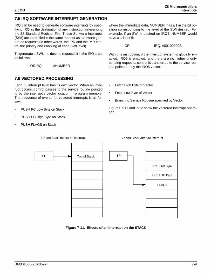
Z8 MicrocontrollersZiLOG Interrupts
7.5 IRQ SOFTWARE INTERRUPT GENERATION
IRQ can be used to generate software interrupts by spec-ifying IRQ as the destination of any instruction referencingthe Z8 Standard Register File. These Software Interrupts(SWI) are controlled in the same manner as hardware gen-erated requests (in other words, the IPR and the IMR con-trol the priority and enabling of each SWI level).
To generate a SWI, the desired request bit in the IRQ is setas follows:
where the immediate data, NUMBER, has a 1 in the bit po-sition corresponding to the level of the SWI desired. Forexample, if an SWI is desired on IRQ5, NUMBER wouldhave a 1 in bit 5:
With this instruction, if the interrupt system is globally en-abled, IRQ5 is enabled, and there are no higher prioritypending requests, control is transferred to the service rou-tine pointed to by the IRQ5 vector.
7.6 VECTORED PROCESSING
Each Z8 interrupt level has its own vector. When an inter-rupt occurs, control passes to the service routine pointedto by the interrupt’s vector location in program memory.The sequence of events for vectored interrupts is as fol-lows:
• PUSH PC Low Byte on Stack
• PUSH PC High Byte on Stack
• PUSH FLAGS on Stack
• Fetch High Byte of Vector
• Fetch Low Byte of Vector
• Branch to Service Routine specified by Vector
Figures 7-11 and 7-12 show the vectored interrupt opera-tion.
ORIRQ, #NUMBER
OR IRQ, #00100000B
Figure 7-11. Effects of an Interrupt on the STACK
SP Top of Stack
PC LOW Byte
PC HIGH Byte
FLAGS
SP and Stack after an interrupt
SP
SP and Stack before an interrupt
UM001600-Z8X0599 7-9
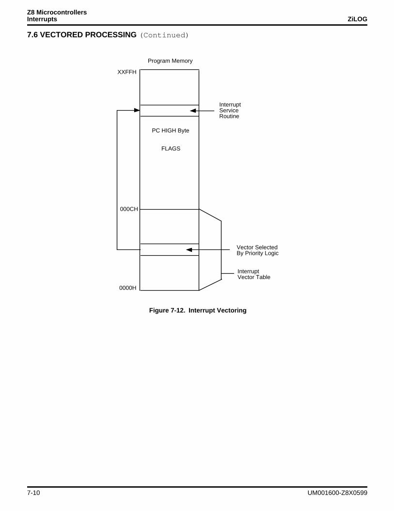
Z8 MicrocontrollersInterrupts ZiLOG
7.6 VECTORED PROCESSING (Continued)
Figure 7-12. Interrupt Vectoring
PC HIGH Byte
FLAGS
Vector Selected
000CH
Program Memory
InterruptServiceRoutine
By Priority Logic
InterruptVector Table
0000H
XXFFH
7-10 UM001600-Z8X0599
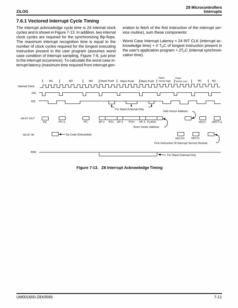
Z8 MicrocontrollersZiLOG Interrupts
7.6.1 Vectored Interrupt Cycle TimingThe interrupt acknowledge cycle time is 24 internal clockcycles and is shown in Figure 7-13. In addition, two internalclock cycles are required for the synchronizing flip-flops.The maximum interrupt recognition time is equal to thenumber of clock cycles required for the longest executinginstruction present in the user program (assumes worstcase condition of interrupt sampling, Figure 7-6, just priorto the interrupt occurrence). To calculate the worst case in-terrupt latency (maximum time required from interrupt gen-
eration to fetch of the first instruction of the interrupt ser-vice routine), sum these components:
Worst Case Interrupt Latency ≈ 24 INT CLK (interrupt ac-knowledge time) + # TPC of longest instruction present inthe user's application program + 2TPC (internal synchroni-zation time).
Figure 7-13. Z8 Interrupt Acknowledge Timing
PC
For Stack External Only
PC+1PC PCLSP-1 SP-2 PCH SP-3 FLAGS VECT VECT+1
Even Vector Address
Odd Vector Address
Op Code (Discarded)VECTH VECTL
First Instruction Of Interrupt Service Routine
For Stack External Only
A0-A7 IN
Internal Clock
/AS
/DS
A0-A7 OUT
M3M1 M2 M1 M2Stack PushFetchVector High
FetchVector LowStack Push Stack Push
R/W
UM001600-Z8X0599 7-11
Z8 MicrocontrollersInterrupts ZiLOG
7.6.2 Nesting of Vectored InterruptsNesting of vectored interrupts allows higher priority re-quests to interrupt a lower priority request. To initiate vec-tored interrupt nesting, do the following during the interruptservice routine:
• Push the old IMR on the stack.
• Load IMR with a new mask to disable lower priorityinterrupts.
• Execute EI instruction.
• Proceed with interrupt processing.
• After processing is complete, execute DI instruction.
• Restore the IMR to its original value by returning theprevious mask from the stack.
• Execute IRET.
Depending on the application, some simplification of theabove procedure may be possible.
7.7 POLLED PROCESSING
Polled interrupt processing is supported by masking off theIRQ to be polled. This is accomplished by clearing the cor-responding bits in the IMR.
To enable any interrupt, first the interrupt mechanism mustbe engaged with an EI instruction. If only polled interruptsare to be serviced, execute:
EI ;Enable interrupt mechanismDI ;Disable vectored interrupts.
To initiate polled processing, check the bits of interest inthe IRQ using the Test Under Mask (TM) instruction. If thebit is set, call or branch to the service routine. The serviceroutine services the request, resets its Request Bit in theIRQ, and branches or returns back to the main program.An example of a polling routine is as follows:
In this example, if IRQ2 is being polled, MASKA will be00000100B and MASKB will be 11111011B.
7.8 RESET CONDITIONS
Upon reset, all bits in IPR are undefined.
In IMR, bit 7 is 0 and bits 0-6 are undefined. The IRQ reg-ister is reset and held in that state until an enable interrupt(EI) instruction is executed.
TM IRQ, #MASKA ;Test for requestJR Z, NEXT ;If no request go to
NEXTCALL SERVICE ;If request is there, then
;service itNEXT:
.
.
.SERVICE: ;Process Request
.
.
.AND IRQ, #MASKB ;Clear Request BitRET ;Return to next
7-12 UM001600-Z8X0599
USER’S MANUAL
CHAPTER 8POWER-DOWN MODES
8.1 INTRODUCTION
In addition to the standard RUN mode, the Z8 MCU® sup-ports two Power-Down modes to minimize device current
consumption. The two modes supported are HALT andSTOP.
8.2 HALT MODE OPERATION
The HALT mode suspends instruction execution and turnsoff the internal CPU clock. The on-chip oscillator circuit re-mains active so the internal clock continues to run and isapplied to the Counter/Timer(s) and interrupt logic.
To enter the HALT mode, it is necessary to first flush theinstruction pipeline to avoid suspending execution in mid-instruction. To do this, the application program must exe-cute a NOP instruction (opcode = FFH) immediately beforethe HALT instruction (opcode 7FH), that is,
The HALT mode is exited by interrupts, either externally orinternally generated. Upon completion of the interrupt ser-vice routine, the user program continues from the instruc-tion after HALT.
The HALT mode may also be exited via a POR/RESET ac-tivation or a Watch-Dog Timer (WDT) timeout. (See theproduct data sheet for WDT availability). In this case, pro-gram execution will restart at the reset restart address000CH.
To further reduce power consumption in the HALT mode,some Z8 family devices allow dynamic internal clock scal-ing. Clock scaling may be accomplished on the fly by re-programming bit 0 and/or bit1 of the STOP-Mode Recov-ery register (SMR). See Figure 8-1.
Note: Internal clock scaling directly effectsCounter/Timer operation — adjustment of the prescalerand downcounter values may be required. To determinethe actual HALT mode current (ICC1) value for the variousoptional modes available, see the related Z8 device’sproduct specification.
FF NOP ;clear the instruction pipeline7F HALT ;enter HALT mode
UM001600-Z8X0599 8-1
Z8 MicrocontrollersPower-Down Modes ZiLOG
8.3 STOP MODE OPERATION
The STOP mode provides the lowest possible devicestandby current. This instruction turns off the on-chip oscil-lator and internal system clock.
To enter the STOP mode, it is necessary to first flush theinstruction pipeline to avoid suspending execution in mid-instruction. To do this, the application program must exe-cute a NOP instruction (opcode=FFH) immediately beforethe STOP instruction (opcode=6FH), that is,
The STOP mode is exited by any one of the following re-sets: Power-On Reset activation, WDT time out (if avail-able), or a STOP-Mode Recovery source. Upon reset gen-eration, the processor will always restart the applicationprogram at address 000CH.
POR/RESET activation is present on all Z8 devices and isimplemented as a reset pin and/or an on-chip power on re-set circuit.
Some Z8 devices allow for the on-chip WDT to run in theSTOP mode. If so activated, the WDT timeout will gener-ate a reset some fixed time period after entering the STOPmode.
Note: STOP-Mode Recovery by the WDT will increasethe STOP mode standby current (ICC2). This is due to theWDT clock and divider circuitry that is now enabled andrunning to support this recovery mode. See the productdata sheet for actual ICC2 values.
All Z8 devices provide some form of dedicated STOP-Mode Recovery (SMR) circuitry. Two SMR methods areimplemented — a single fixed input pin or a flexible, pro-grammable set of inputs. The selected Z8 device productspecification should be reviewed to determine the SMRoptions available for use.
Note: For devices that support SPI, the slave modecompare feature also serves as a SMR source.
In the simple case, a low level applied to input pin P27 willtrigger a SMR. To use this mode, pin P27 (I/O Port 2, bit 7)must be configured as an input before the STOP mode isentered. The low level on P27 must meet a minimum pulsewidth TWSM. (See the product data sheet) to trigger the de-vice reset mode). Some Z8 devices provide multiple SMRinput sources. The desired SMR source is selected via theSMR Register.
Note: Use of specialized SMR modes (P2.7 input orSMR register based) or the WDT timeout (only when in theSTOP mode) provide a unique reset operation. Somecontrol registers are initialized differently for a SMR/WDTtriggered POR than a standard reset operation. See theproduct specification (register file map) for exact details.
To determine the actual STOP mode current (ICC2) valuefor the optional SMR modes available, see the selected Z8device’s product data sheet.
Note: The STOP mode current (ICC2) will be minimizedwhen:
• VCC is at the low end of the devices operating range.
• WDT is off in the STOP mode.
• Output current sourcing is minimized.
• All inputs (digital and analog) are at the low or high railvoltages.
FF NOP ;clear the instruction pipeline6F STOP ;enter STOP mode
8-2 UM001600-Z8X0599
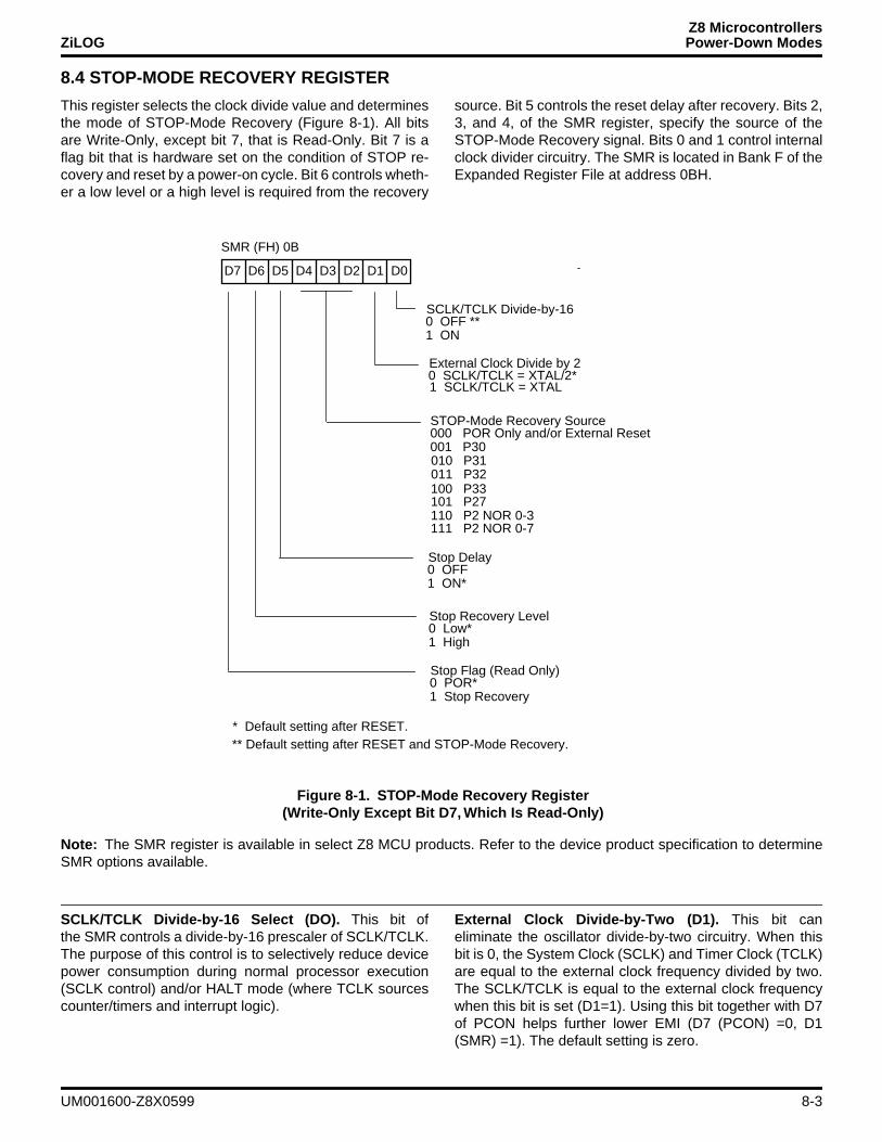
Z8 MicrocontrollersZiLOG Power-Down Modes
8.4 STOP-MODE RECOVERY REGISTER
This register selects the clock divide value and determinesthe mode of STOP-Mode Recovery (Figure 8-1). All bitsare Write-Only, except bit 7, that is Read-Only. Bit 7 is aflag bit that is hardware set on the condition of STOP re-covery and reset by a power-on cycle. Bit 6 controls wheth-er a low level or a high level is required from the recovery
source. Bit 5 controls the reset delay after recovery. Bits 2,3, and 4, of the SMR register, specify the source of theSTOP-Mode Recovery signal. Bits 0 and 1 control internalclock divider circuitry. The SMR is located in Bank F of theExpanded Register File at address 0BH.
Note: The SMR register is available in select Z8 MCU products. Refer to the device product specification to determineSMR options available.
SCLK/TCLK Divide-by-16 Select (DO). This bit ofthe SMR controls a divide-by-16 prescaler of SCLK/TCLK.The purpose of this control is to selectively reduce devicepower consumption during normal processor execution(SCLK control) and/or HALT mode (where TCLK sourcescounter/timers and interrupt logic).
External Clock Divide-by-Two (D1). This bit caneliminate the oscillator divide-by-two circuitry. When thisbit is 0, the System Clock (SCLK) and Timer Clock (TCLK)are equal to the external clock frequency divided by two.The SCLK/TCLK is equal to the external clock frequencywhen this bit is set (D1=1). Using this bit together with D7of PCON helps further lower EMI (D7 (PCON) =0, D1(SMR) =1). The default setting is zero.
Figure 8-1. STOP-Mode Recovery Register (Write-Only Except Bit D7, Which Is Read-Only)
D7 D6 D5 D4 D3 D2 D1 D0
SMR (FH) 0B
STOP-Mode Recovery Source
000 POR Only and/or External Reset 001 P30
010 P31 011 P32
100 P33 101 P27
110 P2 NOR 0-3 111 P2 NOR 0-7
0 OFF ** 1 ON SCLK/TCLK Divide-by-16
0 OFF 1 ON* Stop Delay
0 POR* 1 Stop Recovery Stop Flag (Read Only)
0 SCLK/TCLK = XTAL/2* External Clock Divide by 2
0 Low* 1 High Stop Recovery Level
1 SCLK/TCLK = XTAL
* Default setting after RESET. ** Default setting after RESET and STOP-Mode Recovery.
UM001600-Z8X0599 8-3
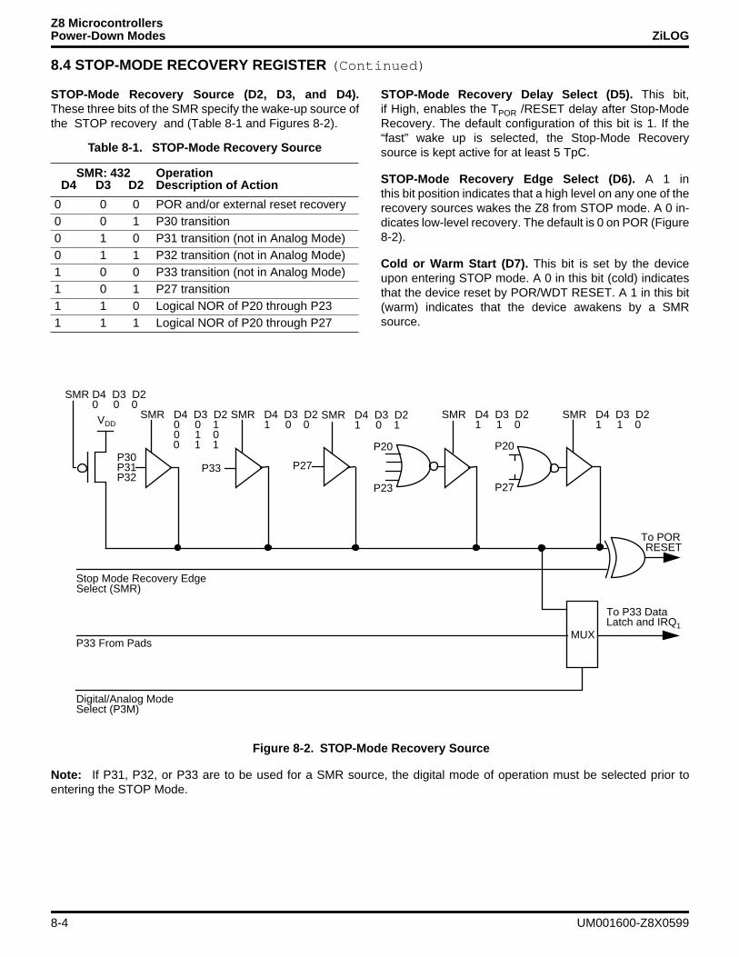
Z8 MicrocontrollersPower-Down Modes ZiLOG
8.4 STOP-MODE RECOVERY REGISTER (Continued)
STOP-Mode Recovery Source (D2, D3, and D4).These three bits of the SMR specify the wake-up source ofthe STOP recovery and (Table 8-1 and Figures 8-2).
STOP-Mode Recovery Delay Select (D5). This bit,if High, enables the TPOR /RESET delay after Stop-ModeRecovery. The default configuration of this bit is 1. If the“fast” wake up is selected, the Stop-Mode Recoverysource is kept active for at least 5 TpC.
STOP-Mode Recovery Edge Select (D6). A 1 inthis bit position indicates that a high level on any one of therecovery sources wakes the Z8 from STOP mode. A 0 in-dicates low-level recovery. The default is 0 on POR (Figure8-2).
Cold or Warm Start (D7). This bit is set by the deviceupon entering STOP mode. A 0 in this bit (cold) indicatesthat the device reset by POR/WDT RESET. A 1 in this bit(warm) indicates that the device awakens by a SMRsource.
Note: If P31, P32, or P33 are to be used for a SMR source, the digital mode of operation must be selected prior toentering the STOP Mode.
Table 8-1. STOP-Mode Recovery Source
SMR: 432 Operation D4 D3 D2 Description of Action
0 0 0 POR and/or external reset recovery0 0 1 P30 transition0 1 0 P31 transition (not in Analog Mode)0 1 1 P32 transition (not in Analog Mode)1 0 0 P33 transition (not in Analog Mode)1 0 1 P27 transition1 1 0 Logical NOR of P20 through P231 1 1 Logical NOR of P20 through P27
Figure 8-2. STOP-Mode Recovery Source
SMR D4 D3 D2 0 0 0
SMR D4 D3 D2 0 0 1 0 1 0 0 1 1
SMR D4 D3 D2 1 0 0
SMR D4 D3 D2 1 0 1
SMR D4 D3 D2 1 1 0
SMR D4 D3 D2 1 1 0VDD
P20
P23
P20
P27
P30P33 P27P31
P32
MUX
To PORRESET
To P33 DataLatch and IRQ1
Stop Mode Recovery EdgeSelect (SMR)
P33 From Pads
Digital/Analog ModeSelect (P3M)
8-4 UM001600-Z8X0599
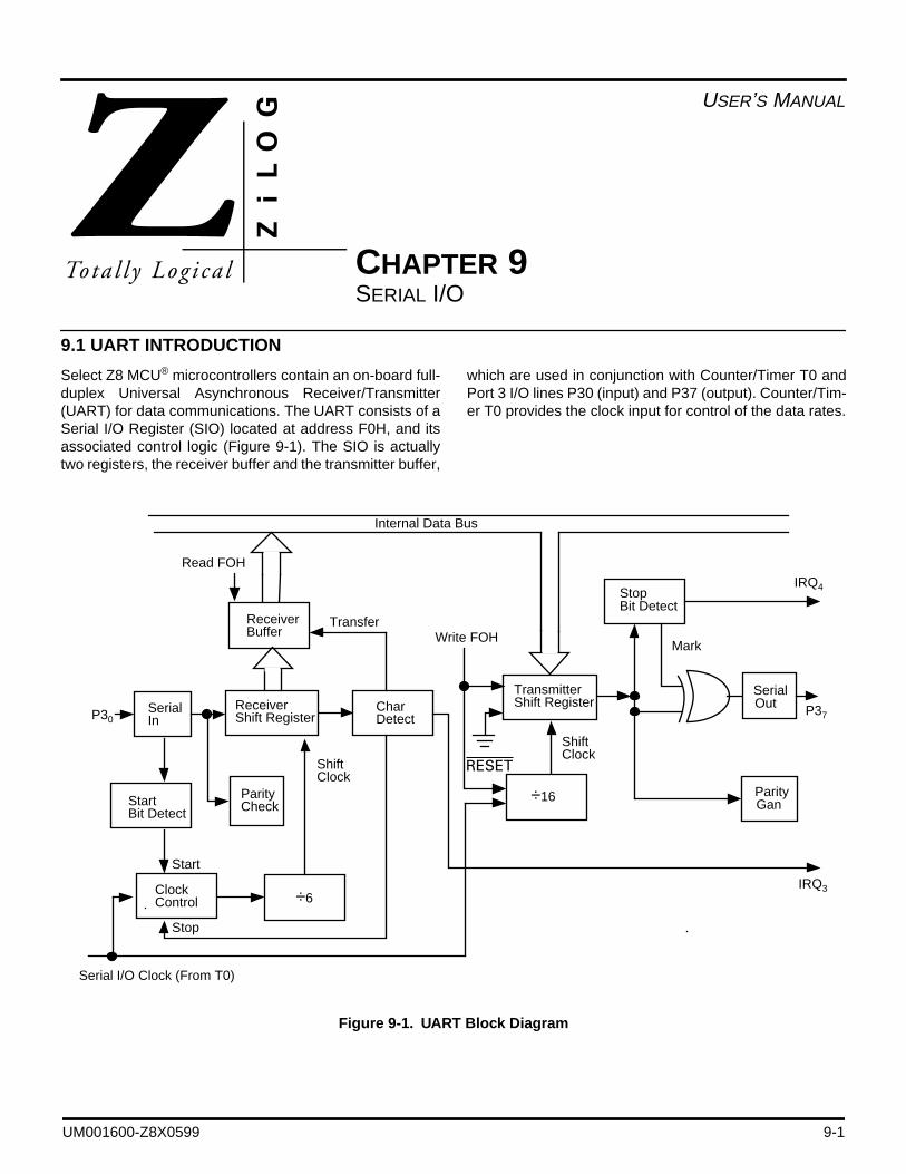
USER’S MANUAL
CHAPTER 9SERIAL I/O
9.1 UART INTRODUCTION
Select Z8 MCU® microcontrollers contain an on-board full-duplex Universal Asynchronous Receiver/Transmitter(UART) for data communications. The UART consists of aSerial I/O Register (SIO) located at address F0H, and itsassociated control logic (Figure 9-1). The SIO is actuallytwo registers, the receiver buffer and the transmitter buffer,
which are used in conjunction with Counter/Timer T0 andPort 3 I/O lines P30 (input) and P37 (output). Counter/Tim-er T0 provides the clock input for control of the data rates.
Figure 9-1. UART Block Diagram
StopBit Detect
TransmitterShift Register
÷6
ParityGan
SerialOutChar
Detect
Receiver Buffer
ReceiverShift Register
SerialIn
StartBit Detect
ClockControl
ParityCheck
ShiftClock
ShiftClock
÷16
Transfer
Stop
Start
Write FOH
RESET
Read FOH
Mark
Serial I/O Clock (From T0)
IRQ4
Internal Data Bus
IRQ3
P37P30
UM001600-Z8X0599 9-1
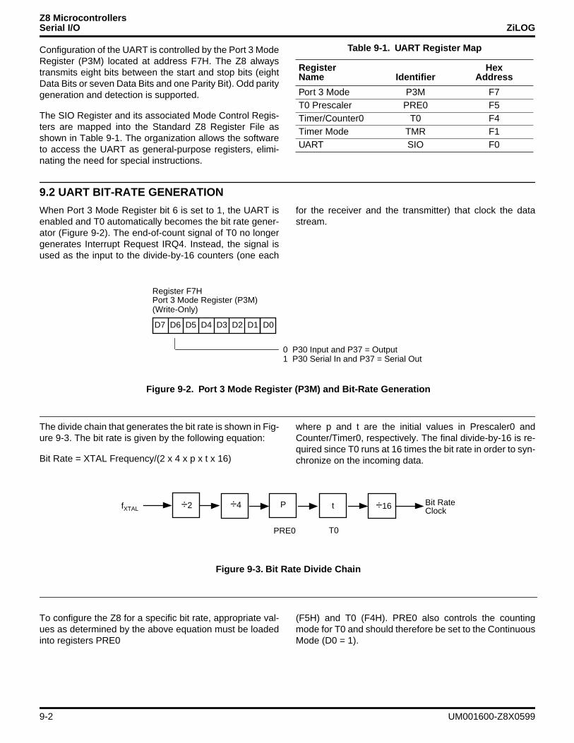
Z8 MicrocontrollersSerial I/O ZiLOG
Configuration of the UART is controlled by the Port 3 ModeRegister (P3M) located at address F7H. The Z8 alwaystransmits eight bits between the start and stop bits (eightData Bits or seven Data Bits and one Parity Bit). Odd paritygeneration and detection is supported.
The SIO Register and its associated Mode Control Regis-ters are mapped into the Standard Z8 Register File asshown in Table 9-1. The organization allows the softwareto access the UART as general-purpose registers, elimi-nating the need for special instructions.
9.2 UART BIT-RATE GENERATION
When Port 3 Mode Register bit 6 is set to 1, the UART isenabled and T0 automatically becomes the bit rate gener-ator (Figure 9-2). The end-of-count signal of T0 no longergenerates Interrupt Request IRQ4. Instead, the signal isused as the input to the divide-by-16 counters (one each
for the receiver and the transmitter) that clock the datastream.
The divide chain that generates the bit rate is shown in Fig-ure 9-3. The bit rate is given by the following equation:
Bit Rate = XTAL Frequency/(2 x 4 x p x t x 16)
where p and t are the initial values in Prescaler0 andCounter/Timer0, respectively. The final divide-by-16 is re-quired since T0 runs at 16 times the bit rate in order to syn-chronize on the incoming data.
To configure the Z8 for a specific bit rate, appropriate val-ues as determined by the above equation must be loadedinto registers PRE0
(F5H) and T0 (F4H). PRE0 also controls the countingmode for T0 and should therefore be set to the ContinuousMode (D0 = 1).
Table 9-1. UART Register Map
Register HexName Identifier Address
Port 3 Mode P3M F7T0 Prescaler PRE0 F5Timer/Counter0 T0 F4Timer Mode TMR F1UART SIO F0
Figure 9-2. Port 3 Mode Register (P3M) and Bit-Rate Generation
D7 D6 D5 D4 D3 D2 D1 D0
(Write-Only)
Port 3 Mode Register (P3M)Register F7H
0 P30 Input and P37 = Output 1 P30 Serial In and P37 = Serial Out
Figure 9-3. Bit Rate Divide Chain
P t ÷16 Bit Rate ÷4 ÷2Clock
PRE0 T0
fXTAL
9-2 UM001600-Z8X0599
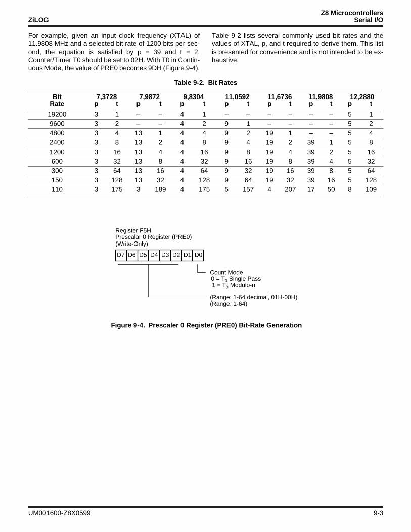
Z8 MicrocontrollersZiLOG Serial I/O
For example, given an input clock frequency (XTAL) of11.9808 MHz and a selected bit rate of 1200 bits per sec-ond, the equation is satisfied by p = 39 and t = 2.Counter/Timer T0 should be set to 02H. With T0 in Contin-uous Mode, the value of PRE0 becomes 9DH (Figure 9-4).
Table 9-2 lists several commonly used bit rates and thevalues of XTAL, p, and t required to derive them. This listis presented for convenience and is not intended to be ex-haustive.
Table 9-2. Bit Rates
Bit 7,3728 7,9872 9,8304 11,0592 11,6736 11,9808 12,2880Rate p t p t p t p t p t p t p t
19200 3 1 – – 4 1 – – – – – – 5 19600 3 2 – – 4 2 9 1 – – – – 5 24800 3 4 13 1 4 4 9 2 19 1 – – 5 42400 3 8 13 2 4 8 9 4 19 2 39 1 5 81200 3 16 13 4 4 16 9 8 19 4 39 2 5 16600 3 32 13 8 4 32 9 16 19 8 39 4 5 32300 3 64 13 16 4 64 9 32 19 16 39 8 5 64150 3 128 13 32 4 128 9 64 19 32 39 16 5 128110 3 175 3 189 4 175 5 157 4 207 17 50 8 109
Figure 9-4. Prescaler 0 Register (PRE0) Bit-Rate Generation
D7 D6 D5 D4 D3 D2 D1 D0
(Write-Only)
Prescalar 0 Register (PRE0)Register F5H
Count Mode 0 = T0 Single Pass
(Range: 1-64 decimal, 01H-00H) (Range: 1-64)
1 = T0 Modulo-n
UM001600-Z8X0599 9-3
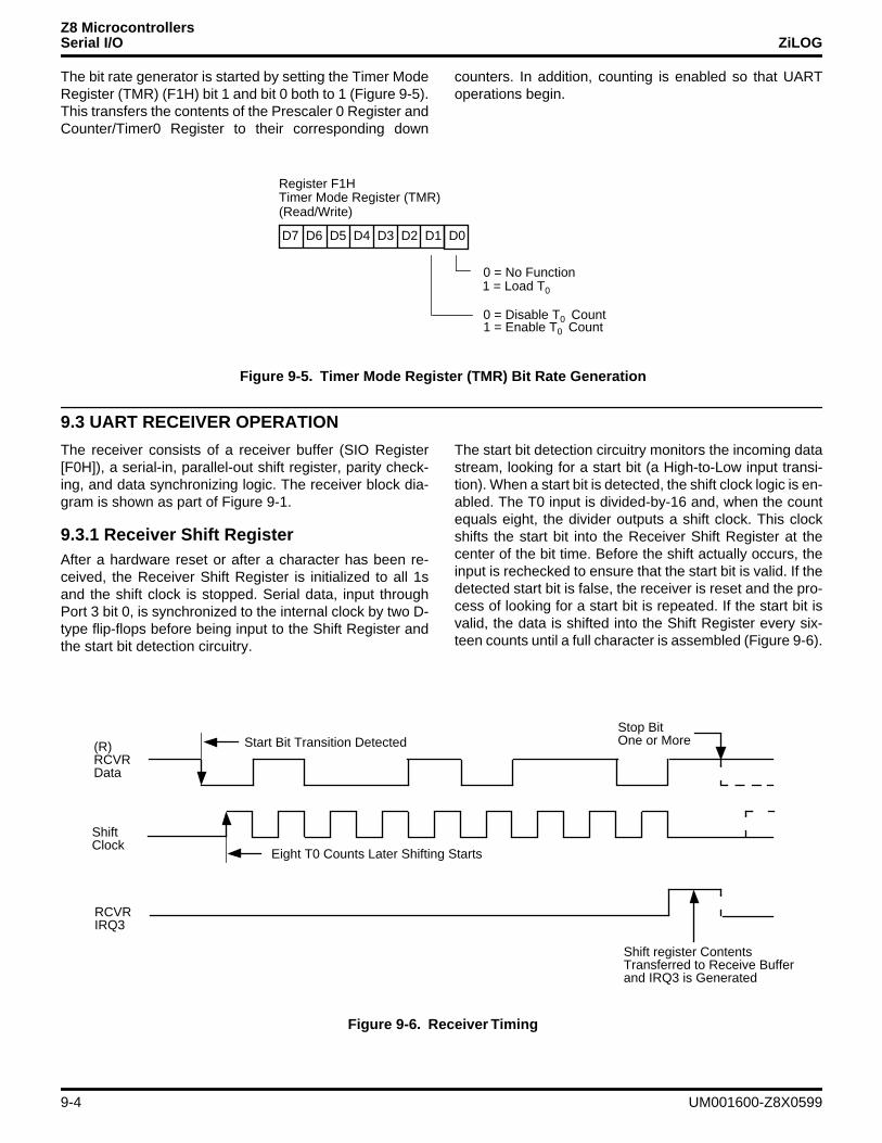
Z8 MicrocontrollersSerial I/O ZiLOG
The bit rate generator is started by setting the Timer ModeRegister (TMR) (F1H) bit 1 and bit 0 both to 1 (Figure 9-5).This transfers the contents of the Prescaler 0 Register andCounter/Timer0 Register to their corresponding down
counters. In addition, counting is enabled so that UARToperations begin.
9.3 UART RECEIVER OPERATION
The receiver consists of a receiver buffer (SIO Register[F0H]), a serial-in, parallel-out shift register, parity check-ing, and data synchronizing logic. The receiver block dia-gram is shown as part of Figure 9-1.
9.3.1 Receiver Shift RegisterAfter a hardware reset or after a character has been re-ceived, the Receiver Shift Register is initialized to all 1sand the shift clock is stopped. Serial data, input throughPort 3 bit 0, is synchronized to the internal clock by two D-type flip-flops before being input to the Shift Register andthe start bit detection circuitry.
The start bit detection circuitry monitors the incoming datastream, looking for a start bit (a High-to-Low input transi-tion). When a start bit is detected, the shift clock logic is en-abled. The T0 input is divided-by-16 and, when the countequals eight, the divider outputs a shift clock. This clockshifts the start bit into the Receiver Shift Register at thecenter of the bit time. Before the shift actually occurs, theinput is rechecked to ensure that the start bit is valid. If thedetected start bit is false, the receiver is reset and the pro-cess of looking for a start bit is repeated. If the start bit isvalid, the data is shifted into the Shift Register every six-teen counts until a full character is assembled (Figure 9-6).
Figure 9-5. Timer Mode Register (TMR) Bit Rate Generation
D7 D6 D5 D4 D3 D2 D1 D0
(Read/Write)
0 = No Function 1 = Load T0
Timer Mode Register (TMR)Register F1H
0 = Disable T0 Count 1 = Enable T0 Count
Figure 9-6. Receiver Timing
Shift register Contents
(R)
Shift
RCVR
Start Bit Transition Detected
Eight T0 Counts Later Shifting Starts
Stop BitOne or More
Transferred to Receive Bufferand IRQ3 is Generated
RCVRData
Clock
IRQ3
9-4 UM001600-Z8X0599
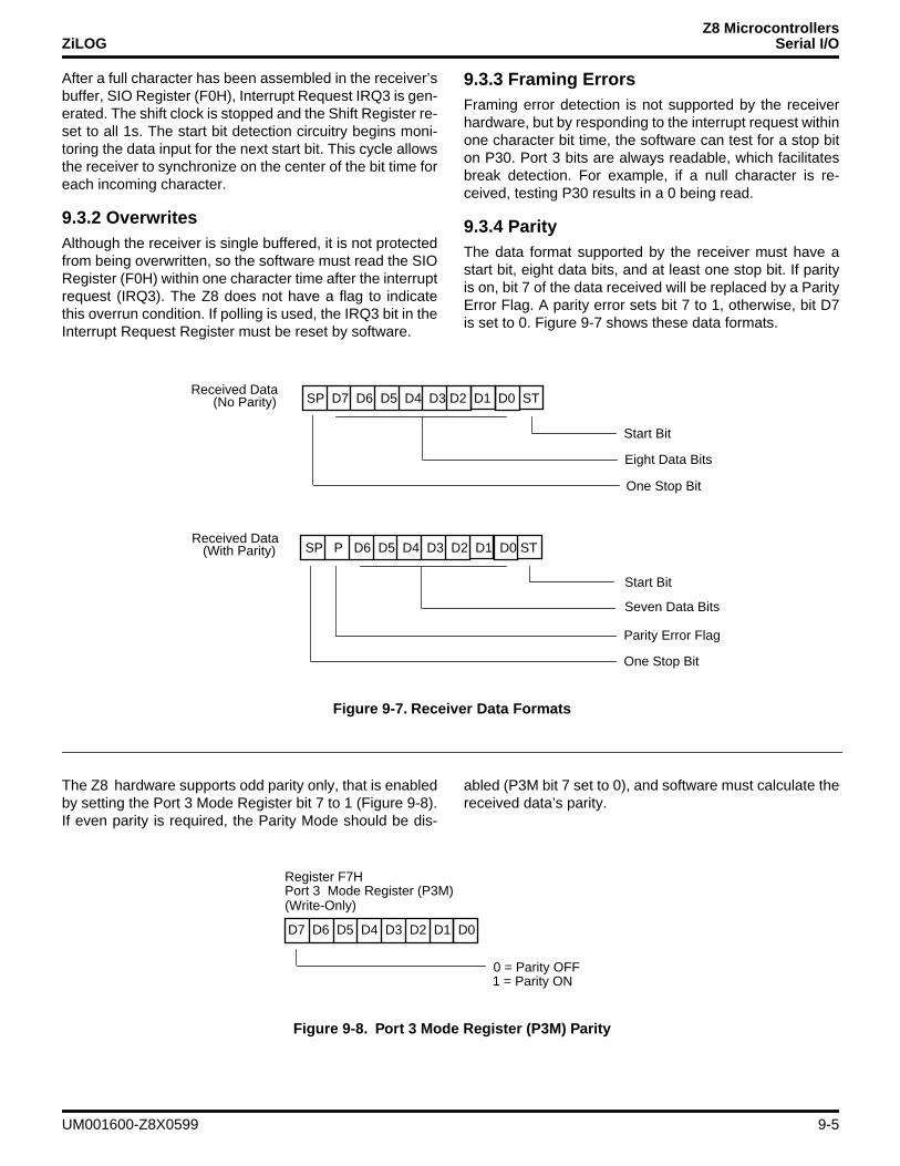
Z8 MicrocontrollersZiLOG Serial I/O
After a full character has been assembled in the receiver’sbuffer, SIO Register (F0H), Interrupt Request IRQ3 is gen-erated. The shift clock is stopped and the Shift Register re-set to all 1s. The start bit detection circuitry begins moni-toring the data input for the next start bit. This cycle allowsthe receiver to synchronize on the center of the bit time foreach incoming character.
9.3.2 OverwritesAlthough the receiver is single buffered, it is not protectedfrom being overwritten, so the software must read the SIORegister (F0H) within one character time after the interruptrequest (IRQ3). The Z8 does not have a flag to indicatethis overrun condition. If polling is used, the IRQ3 bit in theInterrupt Request Register must be reset by software.
9.3.3 Framing ErrorsFraming error detection is not supported by the receiverhardware, but by responding to the interrupt request withinone character bit time, the software can test for a stop biton P30. Port 3 bits are always readable, which facilitatesbreak detection. For example, if a null character is re-ceived, testing P30 results in a 0 being read.
9.3.4 ParityThe data format supported by the receiver must have astart bit, eight data bits, and at least one stop bit. If parityis on, bit 7 of the data received will be replaced by a ParityError Flag. A parity error sets bit 7 to 1, otherwise, bit D7is set to 0. Figure 9-7 shows these data formats.
The Z8 hardware supports odd parity only, that is enabledby setting the Port 3 Mode Register bit 7 to 1 (Figure 9-8).If even parity is required, the Parity Mode should be dis-
abled (P3M bit 7 set to 0), and software must calculate thereceived data’s parity.
Figure 9-7. Receiver Data Formats
SP D7 D6 D5 D4 D3 D2 D1 D0 ST
Eight Data Bits
Start Bit
Start Bit
Seven Data Bits
One Stop Bit
SP P D6 D5 D4 D3 D2 D1 D0 ST
Parity Error Flag
One Stop Bit
Received Data (No Parity)
Received Data (With Parity)
Figure 9-8. Port 3 Mode Register (P3M) Parity
D7 D6 D5 D4 D3 D2 D1 D0
(Write-Only)
0 = Parity OFF 1 = Parity ON
Port 3 Mode Register (P3M)Register F7H
UM001600-Z8X0599 9-5
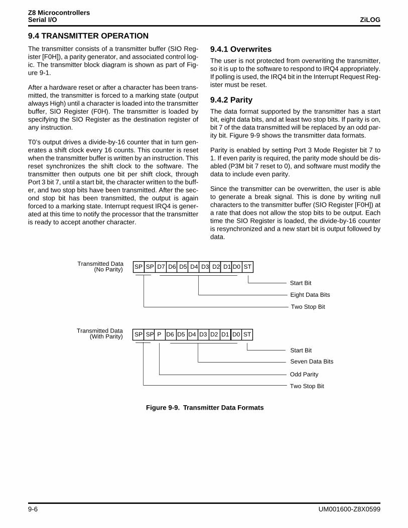
Z8 MicrocontrollersSerial I/O ZiLOG
9.4 TRANSMITTER OPERATION
The transmitter consists of a transmitter buffer (SIO Reg-ister [F0H]), a parity generator, and associated control log-ic. The transmitter block diagram is shown as part of Fig-ure 9-1.
After a hardware reset or after a character has been trans-mitted, the transmitter is forced to a marking state (outputalways High) until a character is loaded into the transmitterbuffer, SIO Register (F0H). The transmitter is loaded byspecifying the SIO Register as the destination register ofany instruction.
T0’s output drives a divide-by-16 counter that in turn gen-erates a shift clock every 16 counts. This counter is resetwhen the transmitter buffer is written by an instruction. Thisreset synchronizes the shift clock to the software. Thetransmitter then outputs one bit per shift clock, throughPort 3 bit 7, until a start bit, the character written to the buff-er, and two stop bits have been transmitted. After the sec-ond stop bit has been transmitted, the output is againforced to a marking state. Interrupt request IRQ4 is gener-ated at this time to notify the processor that the transmitteris ready to accept another character.
9.4.1 OverwritesThe user is not protected from overwriting the transmitter,so it is up to the software to respond to IRQ4 appropriately.If polling is used, the IRQ4 bit in the Interrupt Request Reg-ister must be reset.
9.4.2 ParityThe data format supported by the transmitter has a startbit, eight data bits, and at least two stop bits. If parity is on,bit 7 of the data transmitted will be replaced by an odd par-ity bit. Figure 9-9 shows the transmitter data formats.
Parity is enabled by setting Port 3 Mode Register bit 7 to1. If even parity is required, the parity mode should be dis-abled (P3M bit 7 reset to 0), and software must modify thedata to include even parity.
Since the transmitter can be overwritten, the user is ableto generate a break signal. This is done by writing nullcharacters to the transmitter buffer (SIO Register [F0H]) ata rate that does not allow the stop bits to be output. Eachtime the SIO Register is loaded, the divide-by-16 counteris resynchronized and a new start bit is output followed bydata.
Figure 9-9. Transmitter Data Formats
SP SP D7 D6 D5 D4 D3 D2 D1 D0 ST
Eight Data Bits
Start Bit
Start Bit
Seven Data Bits
Two Stop Bit
SP SP P D6 D5 D4 D3 D2 D1 D0 ST
Odd Parity
Two Stop Bit
Transmitted Data (No Parity)
Transmitted Data (With Parity)
9-6 UM001600-Z8X0599
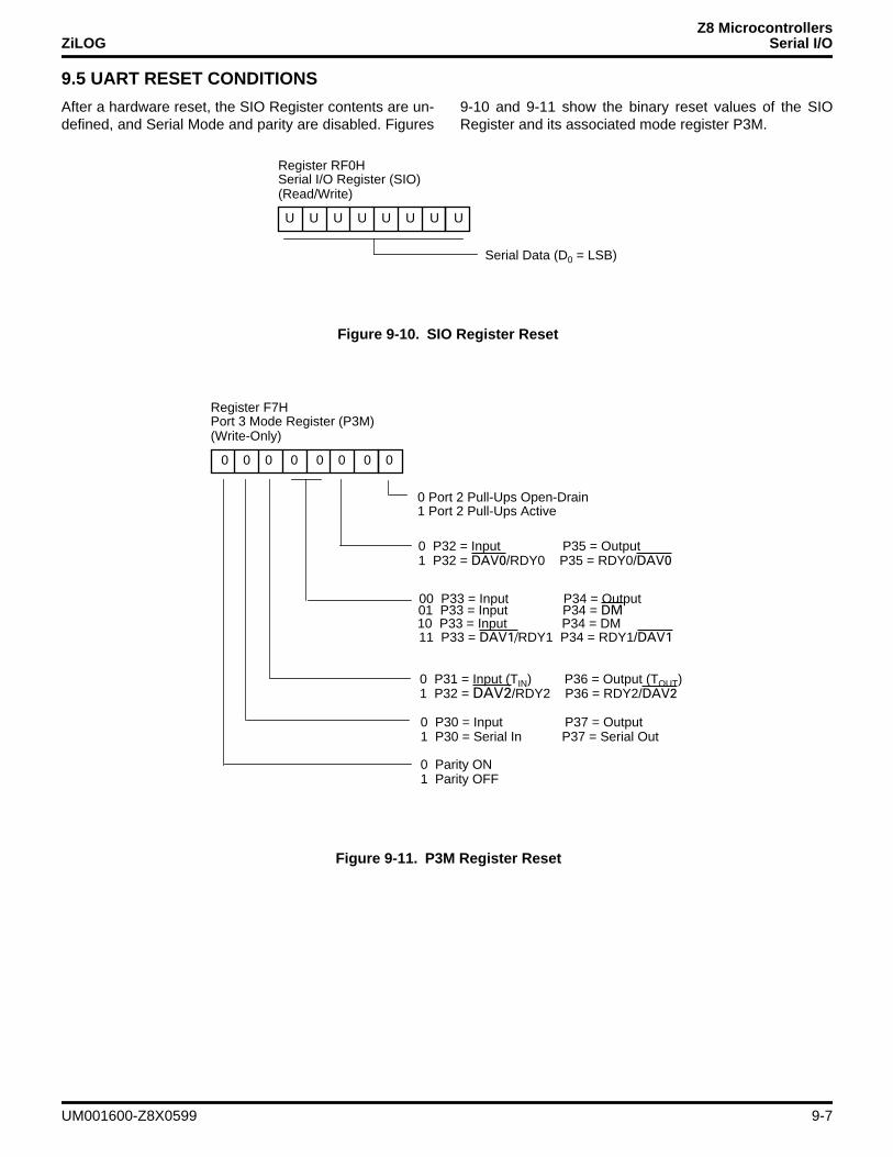
Z8 MicrocontrollersZiLOG Serial I/O
9.5 UART RESET CONDITIONS
After a hardware reset, the SIO Register contents are un-defined, and Serial Mode and parity are disabled. Figures
9-10 and 9-11 show the binary reset values of the SIORegister and its associated mode register P3M.
Figure 9-10. SIO Register Reset
U U U U U U U U
(Read/Write)
Serial Data (D0 = LSB)
Serial I/O Register (SIO)Register RF0H
Figure 9-11. P3M Register Reset
0 0 0 0 0 0 0 0
(Write-Only)
0 P32 = Input P35 = Output 1 P32 = DAV0/RDY0 P35 = RDY0/DAV0
0 Port 2 Pull-Ups Open-Drain 1 Port 2 Pull-Ups Active
00 P33 = Input P34 = Output 01 P33 = Input P34 = DM
Port 3 Mode Register (P3M)Register F7H
10 P33 = Input P34 = DM 11 P33 = DAV1/RDY1 P34 = RDY1/DAV1
0 P31 = Input (TIN) P36 = Output (TOUT) 1 P32 = DAV2/RDY2 P36 = RDY2/DAV2
0 P30 = Input P37 = Output 1 P30 = Serial In P37 = Serial Out
0 Parity ON 1 Parity OFF
UM001600-Z8X0599 9-7
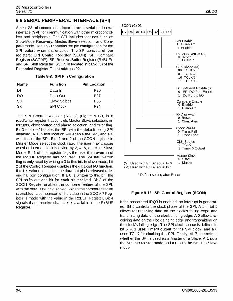
Z8 MicrocontrollersSerial I/O ZiLOG
9.6 SERIAL PERIPHERAL INTERFACE (SPI)
Select Z8 microcontrollers incorporate a serial peripheralinterface (SPI) for communication with other microcontrol-lers and peripherals. The SPI includes features such asStop-Mode Recovery, Master/Slave selection, and Com-pare mode. Table 9-3 contains the pin configuration for theSPI feature when it is enabled. The SPI consists of fourregisters: SPI Control Register (SCON), SPI CompareRegister (SCOMP), SPI Receive/Buffer Register (RxBUF),and SPI Shift Register. SCON is located in bank (C) of theExpanded Register File at address 02.
The SPI Control Register (SCON) (Figure 9-12), is aread/write register that controls Master/Slave selection, in-terrupts, clock source and phase selection, and error flag.Bit 0 enables/disables the SPI with the default being SPIdisabled. A 1 in this location will enable the SPI, and a 0will disable the SPI. Bits 1 and 2 of the SCON register inMaster Mode select the clock rate. The user may choosewhether internal clock is divide-by-2, 4, 8, or 16. In SlaveMode, Bit 1 of this register flags the user if an overrun ofthe RxBUF Register has occurred. The RxCharOverrunflag is only reset by writing a 0 to this bit. In slave mode, bit2 of the Control Register disables the data-out I/O function.If a 1 is written to this bit, the data-out pin is released to itsoriginal port configuration. If a 0 is written to this bit, theSPI shifts out one bit for each bit received. Bit 3 of theSCON Register enables the compare feature of the SPI,with the default being disabled. When the compare featureis enabled, a comparison of the value in the SCOMP Reg-ister is made with the value in the RxBUF Register. Bit 4signals that a receive character is available in the RxBUFRegister.
If the associated IRQ3 is enabled, an interrupt is generat-ed. Bit 5 controls the clock phase of the SPI. A 1 in bit 5allows for receiving data on the clock’s falling edge andtransmitting data on the clock’s rising edge. A 0 allows re-ceiving data on the clock’s rising edge and transmitting onthe clock’s falling edge. The SPI clock source is defined inbit 6. A 1 uses Timer0 output for the SPI clock, and a 0uses TCLK for clocking the SPI. Finally, bit 7 determineswhether the SPI is used as a Master or a Slave. A 1 putsthe SPI into Master mode and a 0 puts the SPI into Slavemode.
Table 9-3. SPI Pin Configuration
Name Function Pin Location
DI Data-In P20DO Data-Out P27SS Slave Select P35SK SPI Clock P34
Figure 9-12. SPI Control Register (SCON)
D7 D6 D5 D4 D3 D2 D1 D0
SCON (C) 02
CLK Divide (M)
00 TCLK/2 01 TCLK/4
10 TCLK/8 11 TCLK/16
DO SPI Port Enable (S) 0 SPI DO Port Enable
1 Do Port to I/O
0 Disable * 1 Enable SPI Enable
0 Enable 1 Disable * Compare Enable
0 Trans/Fall 1 Trans/Rise Clock Phase
0 Reset RxCharOverrun (S)
0 Reset 1 Char. Avail RxCharAvail
1 Overrun
(M) Used with Bit D7 equal to 1
* Default setting after Reset
0 TCLK 1 Timer 0 Output CLK Source
0 Slave 1 Master Master Slave
(S) Used with Bit D7 equal to 0
9-8 UM001600-Z8X0599
Z8 MicrocontrollersZiLOG Serial I/O
9.7 SPI OPERATION
The SPI is used in one of two modes: either as systemslave, or as system master. Several of the possible systemconfigurations are shown in Figure 9-13. In the slavemode, data transfer starts when the slave select (SS) pingoes active. Data is transferred into the slave’s SPI ShiftRegister through the DI pin, which has the same addressas the RxBUF Register. After a byte of data has been re-ceived by the SPI Shift Register, a Receive CharacterAvailable (RCA/IRQ3) flag and interrupt is generated. Thenext byte of data will be received at this time. The RxBUFRegister must be cleared, or a Receive Character Overrun(RxCharOverrun) flag will be set in the SCON Register,and the data in the RxBUF Register will be overwritten.When the communication between the master and slave iscomplete, the SS goes inactive.When the SPI is activatedas a slave, it operates in all system modes: STOP, HALT,and RUN.
Unless disconnected, for every bit that is transferred intothe slave through the DI pin, a bit is transferred out throughthe D0 pin on the opposite clock edge. During slave oper-ation, the SPI clock pin (SK) is an input. In master mode,the CPU must first activate a SS through one of its I/Oports. Next, data is transferred through the master’s D0 pinone bit per master clock cycle. Loading data into the shiftregister initiates the transfer. In master mode, the master’sclock will drive the slave’s clock. At the conclusion of atransfer, a Receive Character Available (RCA/IRQ3) flagand interrupt is generated. Before data is transferred viathe D0 pin, the SPI Enable bit in the SCON Register mustbe enabled.
9.8 SPI COMPARE
When the SPI Compare Enable bit, D3 of the SCON Reg-ister is set to 1, the SPI Compare feature is enabled. Thecompare feature is only valid for slave mode. A comparetransaction begins when the (SS) line goes active. Data isreceived as if it were a normal transaction, but there is nodata transmitted to avoid bus contention with other slavedevices. When the compare byte is received, IRQ3 is notgenerated. Instead, the data is compared with the contentsof the SCOMP Register. If the data does not match, DO re-mains inactive and the slave ignores all data until the (SS)signal is reset. If the data received matches the data in theSCOMP register, then a SMR signal is generated. DO isactivated if it is not tri-stated by D2 in the SCON Register,and data is received the same as any other SPI slavetransaction.
Slaves’ not comparing remain in their current mode,whereas slaves’ comparing wake from a STOP mode bymeans of an SMR
9.9 SPI CLOCK
The SPI clock maybe driven by three sources: Timer0, adivision of the internal system clock, or the external masterwhen in slave mode. Bit D6 of the SCON Register controlswhat source drives the SPI clock. A 0 in bit D6 of the SCONRegister determines the division of the internal systemclock if this is used as the SPI clock source. Divide by 2, 4,8, or 16 is chosen as the scaler.
UM001600-Z8X0599 9-9
Z8 MicrocontrollersSerial I/O ZiLOG
Figure 9-13. SPI System Configuration
ss sk do di
Slave
Multiple slaves may have the same address
ss1
ss4
do
ss2ss3
sk
di
Master
Three Wire Compare Setup
ss sk do di
Slave
ss sk do di
Slave
ss sk do di
Slave
ss
sk
do
di
Master
ss sk do di
Slave
Setup For Compare
ss sk do di
Slave
ss sk do di
Slave
ss sk do di
Slave
ss
sk
do
di
Master
Up to 256 slaves per SS line(1) (2) (255) (256)
ss sk do di
Slave
ss sk do di
Slave
ss sk do di
Slave
ss sk do di
Slave
Standard Parallel Setup
ss sk do di
Slave
Standard Serial Setup
ss sk do di
Slave
ss sk do di
Slave
ss sk do di
Slave
ss
sk
do
di
Master
9-10 UM001600-Z8X0599
Z8 MicrocontrollersZiLOG Serial I/O
9.10 RECEIVE CHARACTER AVAILABLE AND OVERRUN
When a complete data stream is received, an interrupt isgenerated and the RxCharAvail bit in the SCON Registeris set. Bit 4 in the SCON Register is for enabling or dis-abling the RxCharAvail interrupt. The RxCharAvail bit isavailable for interrupt polling purposes and is reset whenthe RxBUF Register is read. RxCharAvail is generated inboth master and slave modes. While in slave mode, if theRxBUF is not read before the next data stream is receivedand loaded into the RxBUF Register, Receive CharacterOverrun (RxCharOverrun) occurs. Since there is no needfor clock control in slave mode, bit D1 in the SPI Control
Register is used to log any RxCharOverrun (Figure 9-14and Figure 9-15).
No Parameter Min Units
1 DI to SK Setup 10 ns2 SK to D0 Valid 15 ns3 SS to SK Setup .5 Tsk ns4 SS to D0 Valid 15 ns5 SK to DI Hold Time 10 ns
Figure 9-14. SPI Timing
TSK
SS
SK
D0
DI
1
2
3
4
5
UM001600-Z8X0599 9-11
Z8 MicrocontrollersSerial I/O ZiLOG
9.10 RECEIVE CHARACTER AVAILABLE AND OVERRUN (Continued)
Figure 9-15. SPI Logic
SPI Compare Register (SCOMP) SS
D0
DI
SK
Port
TCLK
SMRBit Control
SPI Control
SPI Receive Buffer (RxBUF)
SPI Shift Register
/InterruptControl
IRQ3 SCLK + n
SPIClock
Control
9-12 UM001600-Z8X0599
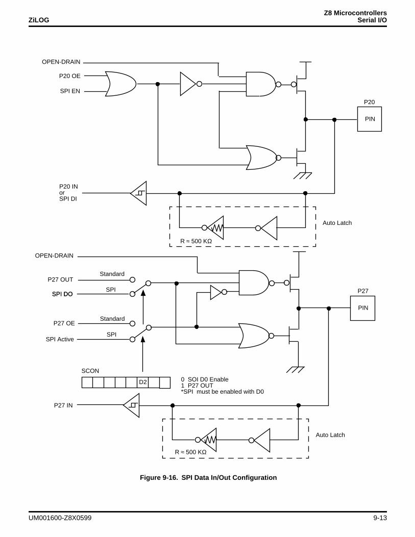
Z8 MicrocontrollersZiLOG Serial I/O
Figure 9-16. SPI Data In/Out Configuration
P27 OUT
PIN
SPI Active
P27 IN
0 SOI D0 Enable
OPEN-DRAIN
Auto Latch
P27
P20 OE
PIN
P20 IN
OPEN-DRAIN
R ≈ 500 KΩ
Auto Latch
P20
SPI EN
SPI DO
P27 OE
SPI
SPI DOSPI
Standard
Standard
1 P27 OUT*SPI must be enabled with D0
D2
SCON
orSPI DI
R ≈ 500 KΩ
UM001600-Z8X0599 9-13

Z8 MicrocontrollersSerial I/O ZiLOG
9.10 RECEIVE CHARACTER AVAILABLE AND OVERRUN (Continued)
Figure 9-17. SPI Clock / SPI Slave Select Output Configuration
SPI MSTR
PIN
P31 +
SPI EN
P34
SK IN
SPI MSTR
PIN
P35
SPI EN
REF SS
0 P34, P35 Standard Output1 P34, P35 Comparator Output D0
P35 OUT
PCON
P32
REF
+-
P34 OUT
-
SPI EN
SK OUTMUX
9-14 UM001600-Z8X0599
Z8 MicrocontrollersZiLOG Serial I/O
UM001600-Z8X0599 9-15
Z8 MicrocontrollersSerial I/O ZiLOG
9-16 UM001600-Z8X0599
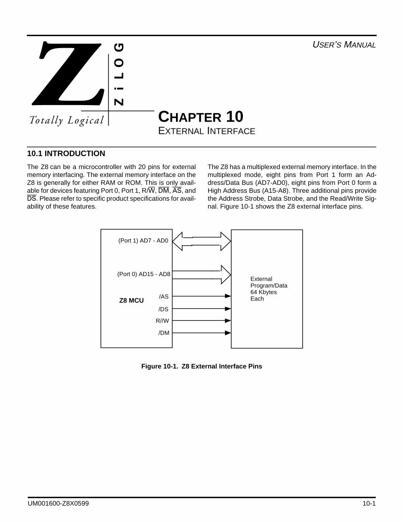
USER’S MANUAL
CHAPTER 10EXTERNAL INTERFACE
10.1 INTRODUCTION
The Z8 can be a microcontroller with 20 pins for externalmemory interfacing. The external memory interface on theZ8 is generally for either RAM or ROM. This is only avail-able for devices featuring Port 0, Port 1, R/W, DM, AS, andDS. Please refer to specific product specifications for avail-ability of these features.
The Z8 has a multiplexed external memory interface. In themultiplexed mode, eight pins from Port 1 form an Ad-dress/Data Bus (AD7-AD0), eight pins from Port 0 form aHigh Address Bus (A15-A8). Three additional pins providethe Address Strobe, Data Strobe, and the Read/Write Sig-nal. Figure 10-1 shows the Z8 external interface pins.
Figure 10-1. Z8 External Interface Pins
External
Z8 MCU
Program/Data64 KbytesEach
(Port 1) AD7 - AD0
(Port 0) AD15 - AD8
/AS
/DS
R//W
/DM
UM001600-Z8X0599 10-1
Z8 MicrocontrollersExternal Interface ZiLOG
10.2 PIN DESCRIPTIONS
The following sections briefly describe the pins associatedwith the Z8 MCU® external memory interface.
10.2.1 /AS Address Strobe (output, active Low). Address Strobe ispulsed Low once at the beginning of each machine cycle.The rising edge of AS indicates the address, Read/Write(R/W), and Data Memory (DM) signals are valid for pro-gram or data memory transfers. In some cases, the Z8 ad-dress strobe is pulsed low regardless of accessing exter-nal or internal memory. Please refer to specific productspecifications for AS operation.
10.2.2 DS Data Strobe (Output, Active Low). Data Strobe providesthe timing for data movement to or from the Address/Databus for each external memory transfer. During a Write Cy-cle, data out is valid at the leading edge of the DS. Duringa Read Cycle, data in must be valid prior to the trailingedge of the DS.
10.2.3 R/W Read/Write (Output). Read/Write determines the directionof data transfer for memory transactions. R/W is Low whenwriting to program or data memory, and High for all othertransactions.
10.2.4 DMData Memory (Output). Data Memory provides a signal toseparate External Program Memory from External DataMemory. It is a programmable function on pin P34. Datamemory is active low for External Data Memory accessesand high for External Program Memory accesses.
10.2.5 P07 - P00 High Address Lines A15 -A8 (Outputs can be CMOS- orTTL- compatible. Please refer to product specifications foractual type). A15-A8 provide the High Address lines for thememory interface. Port 0 - 1 mode register must have bitsD7 = 1 and D1 = 1 to configure Port 0 as A15 - A8 (Figure10-2).
10.2.6 P17 - P10Address/Data Lines AD7 - AD0 (inputs/outputs, TTL-com-patible). AD7-AD0 is a multiplexed Address/Data memoryinterface. The lower eight Address lines (A7-A0) are multi-plexed with Data lines (D7-D0). Port 0 - 1 mode registermust have bits D4 = 1 and D3 = 0 to configure Port 1 asAD7 - AD0 (Figure 10-2).
10.2.7 /RESET Reset (input, active Low). RESET initializes the Z8. WhenRESET is deactivated, program execution begins fromprogram location 000CH. If held Low, RESET acts as aregister file protect during power-down and power-upsequences. To avoid asynchronous and noisy resetproblems, the Z8 is equipped with a reset filter of fourexternal clocks (4TPC). If the external RESET signal is lessthan 4TPC in duration, no reset will occur. On the fifth clockafter the RESET is detected, an internal reset signal islatched and held for an internal register count of 18 ormore external clocks, or for the duration of the externalRESET, whichever is longer. Please refer to specificproduct specifications for length of reset delay time.
10.2.8 XTAL1, XTAL2. Crystal1, Crystal2 (Oscillator input and output). These pinsconnect a parallel-resonant crystal, ceramic resonator, LC,RC network, or external single-phase clock to the on-chiposcillator input. Please refer to the device product specifi-cations for information on availability of RC oscillator fea-tures.
10-2 UM001600-Z8X0599
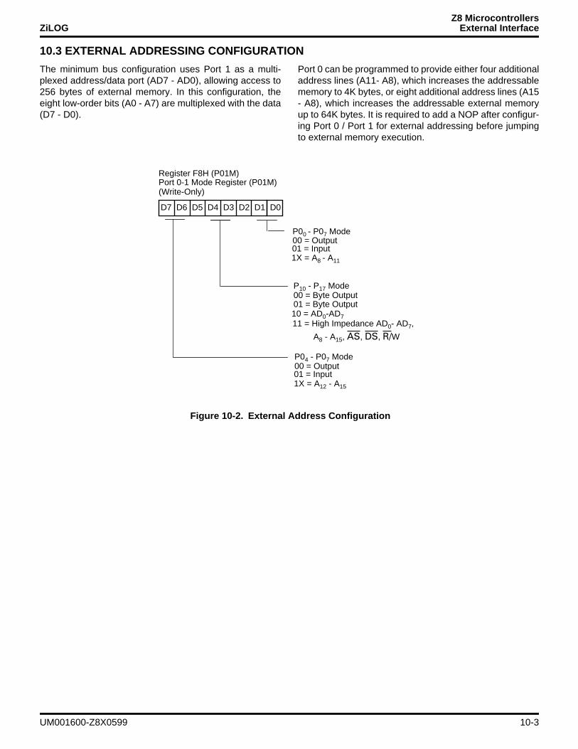
Z8 MicrocontrollersZiLOG External Interface
10.3 EXTERNAL ADDRESSING CONFIGURATION
The minimum bus configuration uses Port 1 as a multi-plexed address/data port (AD7 - AD0), allowing access to256 bytes of external memory. In this configuration, theeight low-order bits (A0 - A7) are multiplexed with the data(D7 - D0).
Port 0 can be programmed to provide either four additionaladdress lines (A11- A8), which increases the addressablememory to 4K bytes, or eight additional address lines (A15- A8), which increases the addressable external memoryup to 64K bytes. It is required to add a NOP after configur-ing Port 0 / Port 1 for external addressing before jumpingto external memory execution.
Figure 10-2. External Address Configuration
D7 D6 D5 D4 D3 D2 D1 D0
(Write-Only)
01 = Input 1X = A8 - A11
P00 - P07 Mode 00 = Output
Port 0-1 Mode Register (P01M)Register F8H (P01M)
01 = Byte Output
P04 - P07 Mode 00 = Output
01 = Input 1X = A12 - A15
10 = AD0-AD7
00 = Byte Output P10 - P17 Mode
A8 - A15, AS, DS, R/W 11 = High Impedance AD0- AD7,
UM001600-Z8X0599 10-3
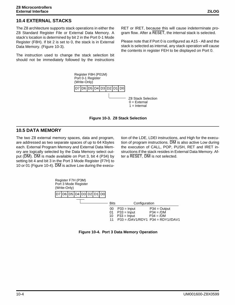
Z8 MicrocontrollersExternal Interface ZiLOG
10.4 EXTERNAL STACKS
The Z8 architecture supports stack operations in either theZ8 Standard Register File or External Data Memory. Astack’s location is determined by bit 2 in the Port 0-1 ModeRegister (F8H). If bit 2 is set to 0, the stack is in ExternalData Memory. (Figure 10-3).
The instruction used to change the stack selection bitshould not be immediately followed by the instructions
RET or IRET, because this will cause indeterminate pro-gram flow. After a RESET, the internal stack is selected.
Please note that if Port 0 is configured as A15 - A8 and thestack is selected as internal, any stack operation will causethe contents in register FEH to be displayed on Port 0.
10.5 DATA MEMORY
The two Z8 external memory spaces, data and program,are addressed as two separate spaces of up to 64 Kbyteseach. External Program Memory and External Data Mem-ory are logically selected by the Data Memory select out-put (DM). DM is made available on Port 3, bit 4 (P34) bysetting bit 4 and bit 3 in the Port 3 Mode Register (F7H) to10 or 01 (Figure 10-4). DM is active Low during the execu-
tion of the LDE, LDEI instructions, and High for the execu-tion of program instructions. DM is also active Low duringthe execution of CALL, POP, PUSH, RET and IRET in-structions if the stack resides in External Data Memory. Af-ter a RESET, DM is not selected.
Figure 10-3. Z8 Stack Selection
D7 D6 D5 D4 D3 D2 D1 D0
(Write-Only)
Port 0-1 Register Register F8H (P01M)
Z8 Stack Selection 0 = External
1 = Internal
Figure 10-4. Port 3 Data Memory Operation
D7 D6 D5 D4 D3 D2 D1 D0
(Write-Only)
Bits Configuration
00 P33 = Input P34 = Output 01 P33 = Input P34 = /DM
Port 3 Mode RegisterRegister F7H (P3M)
10 P33 = Input P34 = /DM 11 P33 = /DAV1/RDY1 P34 = RDY1//DAV1
10-4 UM001600-Z8X0599
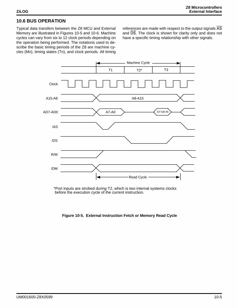
Z8 MicrocontrollersZiLOG External Interface
10.6 BUS OPERATION
Typical data transfers between the Z8 MCU and ExternalMemory are illustrated in Figures 10-5 and 10-6. Machinecycles can vary from six to 12 clock periods depending onthe operation being performed. The notations used to de-scribe the basic timing periods of the Z8 are machine cy-cles (Mn), timing states (Tn), and clock periods. All timing
references are made with respect to the output signals ASand DS. The clock is shown for clarity only and does nothave a specific timing relationship with other signals.
Figure 10-5. External Instruction Fetch or Memory Read Cycle
Machine Cycle
T1 T2* T3
Clock
A15-A8
AD7-AD0
/AS
/DS
R/W
/DM
Read Cycle
A8-A15
A7-A0 D7-D0 IN
*Port inputs are strobed during T2, which is two internal systems clocksbefore the execution cycle of the current instruction.
UM001600-Z8X0599 10-5
Z8 MicrocontrollersExternal Interface ZiLOG
10.6 BUS OPERATION (Continued)
10.6.1 Address Strobe ( AS)All transactions start with AS driven Low and then raisedHigh by the Z8 MCU. The rising edge of AS indicates thatR/W, DM (if used), and the address outputs are valid. Theaddress outputs (AD7-AD0), remain valid only duringMnT1 and typically need to be latched using AS. Addressoutputs (A15-A8) remain stable throughout the machinecycle, regardless of the addressing mode.
10.6.2 Data Strobe (/DS)The Z8 uses DS to time the actual data transfer. For Writeoperations (R/W = Low), a Low on DS indicates that validdata is on the AD7-AD0 lines. For Read operations (R/W =High), the bus is placed in a high-impedance state beforedriving DS Low, so the addressed device can put its dataon the bus. The Z8 samples this data prior to raising DSHigh.
Figure 10-6. External Memory Write Cycle
Machine Cycle
T1 T2 T3
Clock
A15-A8
AD7-AD0
/AS
/DS
R/W
/DM
Write Cycle
A8-A15
A7-A0 D7-D0 OUT
10-6 UM001600-Z8X0599
Z8 MicrocontrollersZiLOG External Interface
10.7 EXTENDED BUS TIMING
Some products can accommodate slow memory accesstime by automatically inserting an additional software con-trolled state time (Tx). This stretches the DS timing by two
clock periods. Figures 10-7 and 10-8 illustrate extendedexternal memory Read and Write cycles.
Figure 10-7. Extended External Instruction Fetch or Memory Read Cycle
Machine Cycle
T2* TX T3
Clock
A15-A8
AD7-AD0
/AS
/DS
R/W
/DM
Read Cycle
A15-A8
A7-A0 D7-D0 IN
T1
*Port inputs are strobed during T2, which is two internal system clocksbefore the execution of the current instruction.
UM001600-Z8X0599 10-7
Z8 MicrocontrollersExternal Interface ZiLOG
Timing is extended by setting bit D5 in the Port 0-1 ModeRegister (F8H) to 1 (Figure 10-9). After a RESET, this bit isset to 0.
Figure 10-8. Extended External Memory Write Cycle
Machine Cycle
T2 TX T3
Clock
A15-A8
AD7-AD0
AS
DS
R/W
DM
Write Cycle
A15-A8
A7-A0 D7-D0 OUT
T1
Figure 10-9. Extended Bus Timing
D7 D6 D5 D4 D3 D2 D1 D0
(Write-Only)
Port 0-1 Register Register F8H (P01M)
External Memory Timing 0 = Normal
1 = Extended
10-8 UM001600-Z8X0599
Z8 MicrocontrollersZiLOG External Interface
10.8 INSTRUCTION TIMING
The High throughput of the Z8 is due, in part, to the use ofan instruction pipeline, in which the instruction fetch andexecution cycles are overlapped. During the execution ofthe current instruction, the opcode of the next instruction isfetched. Instruction pipelining is illustrated in Figure 10-10.
Figures 10-10 and 10-11 show typical instruction cycle tim-ing for instructions fetched from memory. For those in-
structions that require execution time longer than that ofthe overlapped fetch, or reference program or data mem-ory as part of their execution, the pipe must be flushed.
Figures 10-10 and 10-11 assume the XTAL/2 clock modeis selected.
Figure 10-10. Instruction Cycle Timing (One-Byte Instructions)
T1 T2 T3 T3 T1
/DS
/AS
R/W
T1 T2 T2
Fetch 1st Byte
T3
M1 M2 M3
A15-A8A15-A8A15-A8
A7-A0 A7-A0A7-A0A7-A0A7-A0
Fetch 1st Byte Of Next Instruction
* Port inputs are strobed during T2, which is two internal system clocks before the execution cycle of the current installation
Clock
UM001600-Z8X0599 10-9
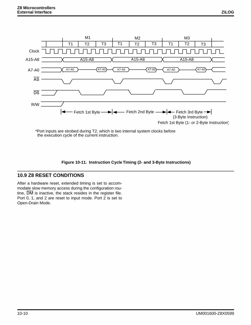
Z8 MicrocontrollersExternal Interface ZiLOG
10.9 Z8 RESET CONDITIONS
After a hardware reset, extended timing is set to accom-modate slow memory access during the configuration rou-tine, DM is inactive, the stack resides in the register file.Port 0, 1, and 2 are reset to input mode. Port 2 is set toOpen-Drain Mode.
Figure 10-11. Instruction Cycle Timing (2- and 3-Byte Instructions)
T1 T2 T3 T3 T1
DS
AS
R/W
T1 T2 T2
Fetch 1st Byte
T3
M1 M2 M3
A15-A8A15-A8A15-A8
A7-A0 A7-A0A7-A0A7-A0A7-A0
Fetch 2nd Byte Fetch 3rd Byte
Fetch 1st Byte (1- or 2-Byte Instruction)(3-Byte Instruction)
A15-A8
A7-A0 A7-A0
Clock
*Port inputs are strobed during T2, which is two internal system clocks beforethe execution cycle of the current instruction.
10-10 UM001600-Z8X0599
USER’S MANUAL
CHAPTER 11ADDRESSING MODES
11.1 INTRODUCTION
11.1.1 Z8 Addressing ModesThe Z8 microcontroller provides six addressing modes:
• Register (R)
• Indirect Register (IR)
• Indexed (X)
• Direct (D)
• Relative (RA)
• Immediate (IM)
With the exception of immediate data and condition codes,all operands are expressed as register file, Program Mem-ory, or Data Memory addresses. Registers are accessedusing 8-bit addresses in the range of 00H-FFH. The Pro-gram Memory or Data Memory is accessed using 16-bitaddresses (register pairs) in the range of 0000H-FFFFH.
Working Registers are accessed using 4-bit addresses inthe range of 0-15 (0H-FH). The address of the register be-ing accessed is formed by the combination of the upperfour bits in the Register Pointer (R253) and the 4-bit work-ing register address supplied by the instruction.
Registers can be used in pairs to designate 16-bit valuesor memory addresses. A Register Pair must be specifiedas an even-numbered address in the range of 0, 2,...., 14for Working Registers, or 4, 6,....238 for actual registers.
In the following definitions of Z8 Addressing Modes, theuse of'register' can also imply register pair, working regis-ter, or working register pair, depending on the context.
Note: See the product data sheet for exact program, data,and register memory types and address ranges available.
UM001600-Z8X0599 11-1
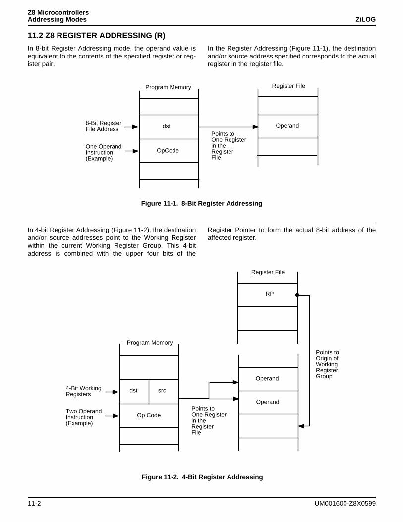
Z8 MicrocontrollersAddressing Modes ZiLOG
11.2 Z8 REGISTER ADDRESSING (R)
In 8-bit Register Addressing mode, the operand value isequivalent to the contents of the specified register or reg-ister pair.
In the Register Addressing (Figure 11-1), the destinationand/or source address specified corresponds to the actualregister in the register file.
In 4-bit Register Addressing (Figure 11-2), the destinationand/or source addresses point to the Working Registerwithin the current Working Register Group. This 4-bitaddress is combined with the upper four bits of the
Register Pointer to form the actual 8-bit address of theaffected register.
Figure 11-1. 8-Bit Register Addressing
OpCodeOne Operand
Register File
Operand
Program Memory
Points todst8-Bit Register
One Registerin theRegisterFile
Instruction(Example)
File Address
Figure 11-2. 4-Bit Register Addressing
Op CodeTwo Operand
Register File
Operand
Program Memory
Points to
src4-Bit Working
One Registerin theRegisterFile
Instruction(Example)
Registers
Operand
RP
dst
Points toOrigin ofWorkingRegisterGroup
11-2 UM001600-Z8X0599
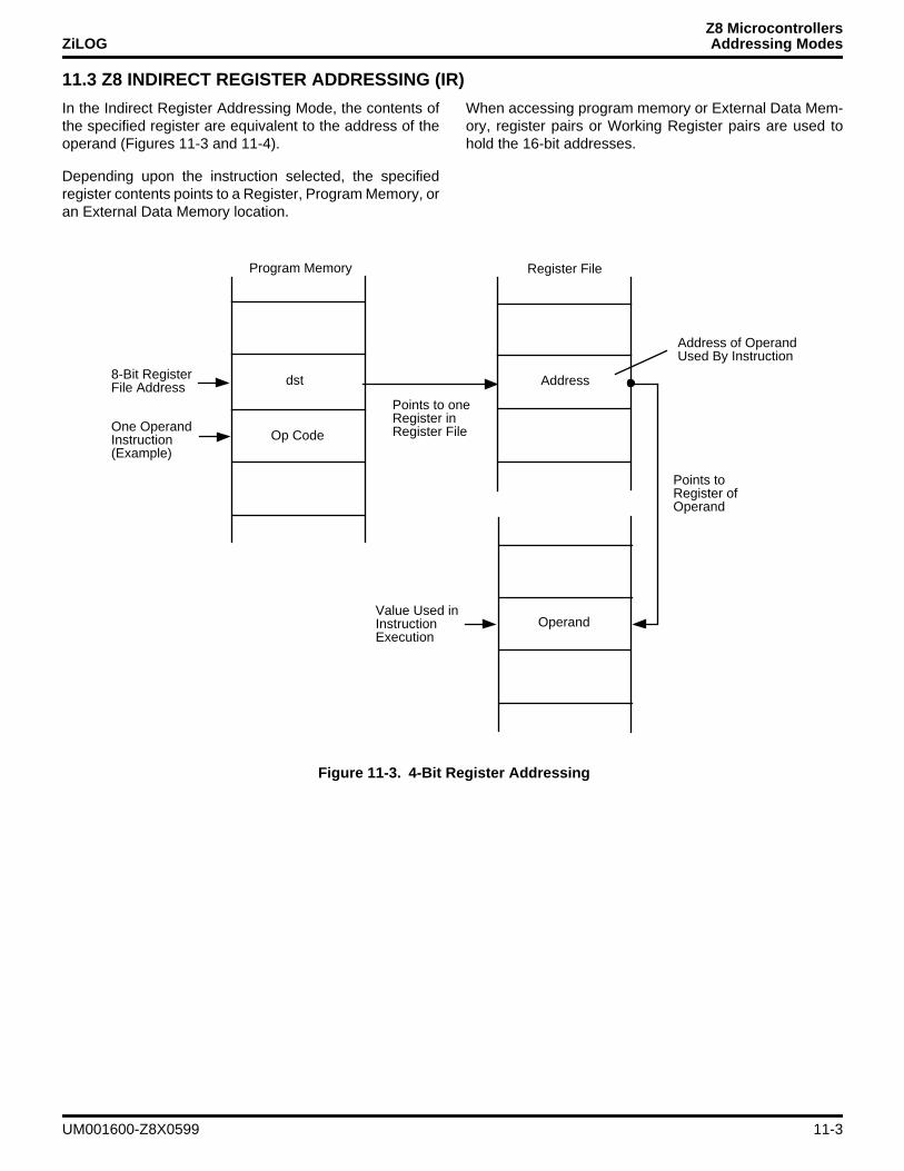
Z8 MicrocontrollersZiLOG Addressing Modes
11.3 Z8 INDIRECT REGISTER ADDRESSING (IR)
In the Indirect Register Addressing Mode, the contents ofthe specified register are equivalent to the address of theoperand (Figures 11-3 and 11-4).
Depending upon the instruction selected, the specifiedregister contents points to a Register, Program Memory, oran External Data Memory location.
When accessing program memory or External Data Mem-ory, register pairs or Working Register pairs are used tohold the 16-bit addresses.
Figure 11-3. 4-Bit Register Addressing
Op CodeOne Operand
Register File
Operand
Program Memory
Points to one
8-Bit Register
Value Used in
Address of Operand
Instruction(Example)
File Address Addressdst
Points toRegister ofOperand
Register inRegister File
InstructionExecution
Used By Instruction
UM001600-Z8X0599 11-3
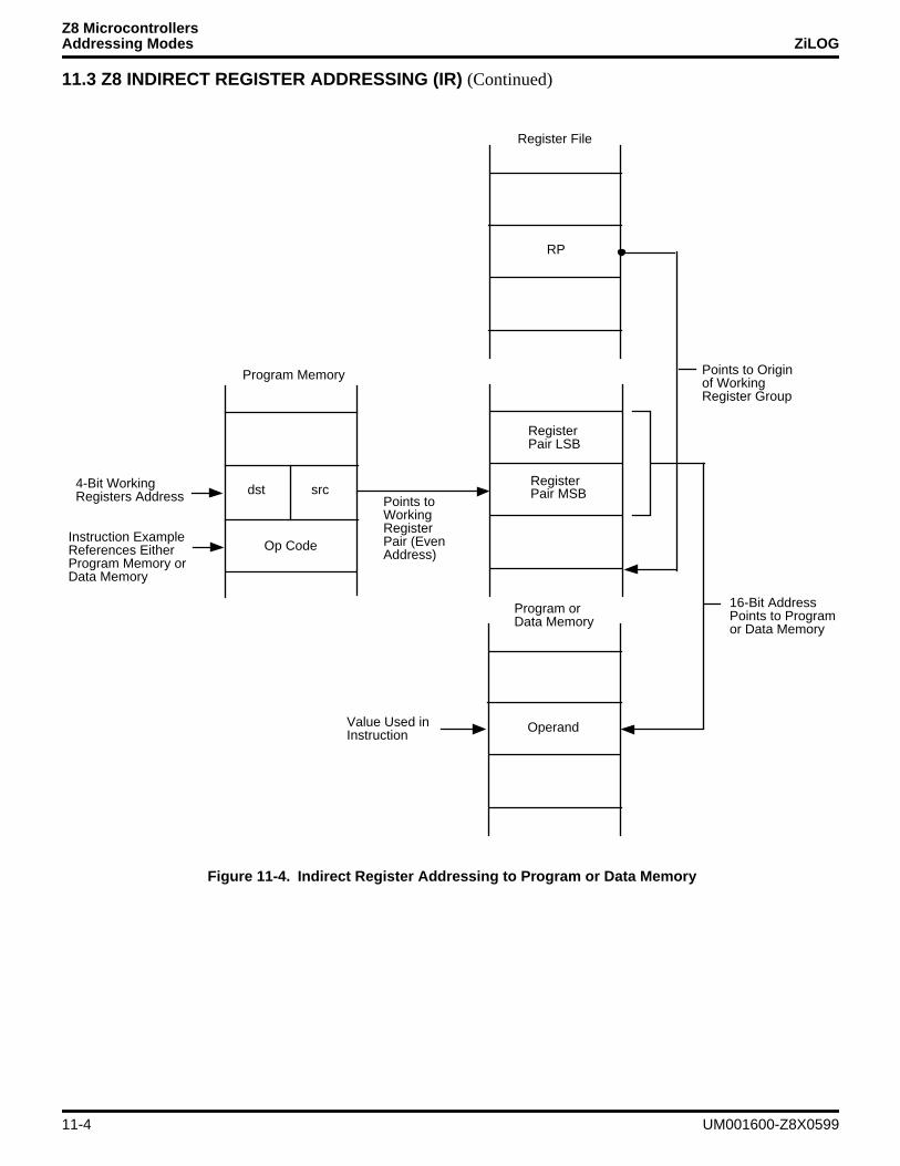
Z8 MicrocontrollersAddressing Modes ZiLOG
11.3 Z8 INDIRECT REGISTER ADDRESSING (IR) (Continued)
Figure 11-4. Indirect Register Addressing to Program or Data Memory
Op CodeInstruction Example
Program or
Register File
Program Memory
Points tosrc4-Bit Working
Points to Origin
Registers Address
Register
dst
RP
Operand
Pair LSB
RegisterPair MSB
Data Memory
WorkingRegisterPair (EvenAddress)
of WorkingRegister Group
16-Bit AddressPoints to Programor Data Memory
References EitherProgram Memory orData Memory
Value Used inInstruction
11-4 UM001600-Z8X0599
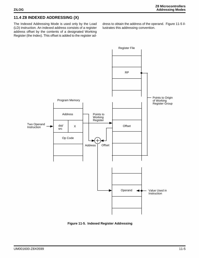
Z8 MicrocontrollersZiLOG Addressing Modes
11.4 Z8 INDEXED ADDRESSING (X)
The Indexed Addressing Mode is used only by the Load(LD) instruction. An indexed address consists of a registeraddress offset by the contents of a designated WorkingRegister (the Index). This offset is added to the register ad-
dress to obtain the address of the operand. Figure 11-5 il-lustrates this addressing convention.
Figure 11-5. Indexed Register Addressing
Op Code
Register File
Program Memory
Points to
src
Two Operand
Points to Origin
Instruction dst/
RP
Operand
Offset
WorkingRegister
OffsetAddress
of WorkingRegister Group
Value Used inInstruction
Address
X
UM001600-Z8X0599 11-5
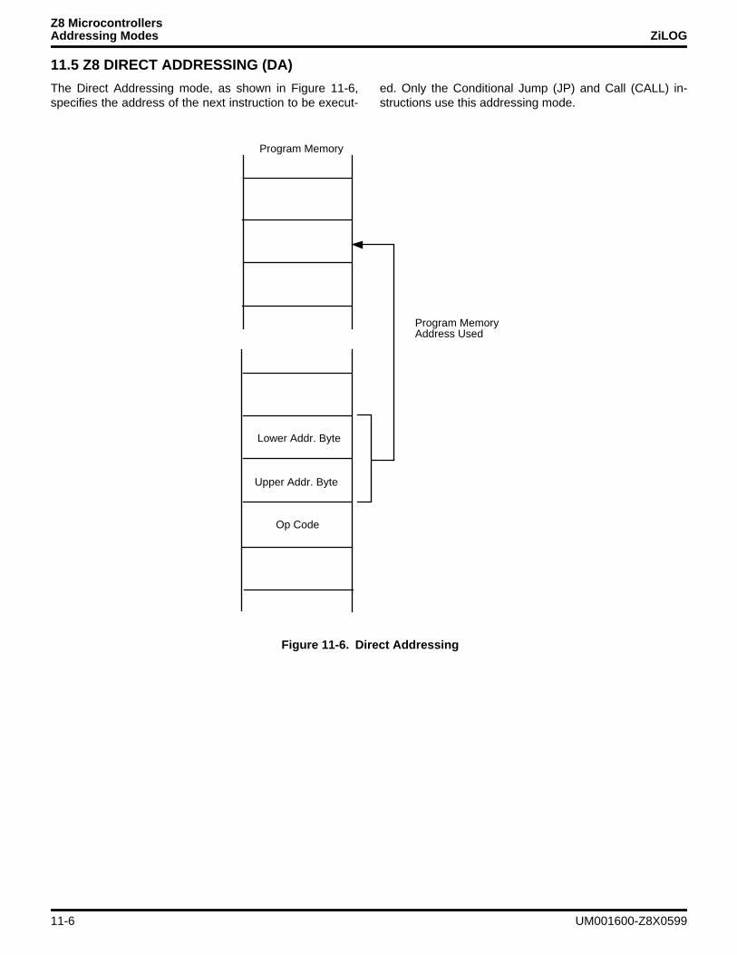
Z8 MicrocontrollersAddressing Modes ZiLOG
11.5 Z8 DIRECT ADDRESSING (DA)
The Direct Addressing mode, as shown in Figure 11-6,specifies the address of the next instruction to be execut-
ed. Only the Conditional Jump (JP) and Call (CALL) in-structions use this addressing mode.
Figure 11-6. Direct Addressing
Op Code
Upper Addr. Byte
Lower Addr. Byte
Program Memory
Program MemoryAddress Used
11-6 UM001600-Z8X0599
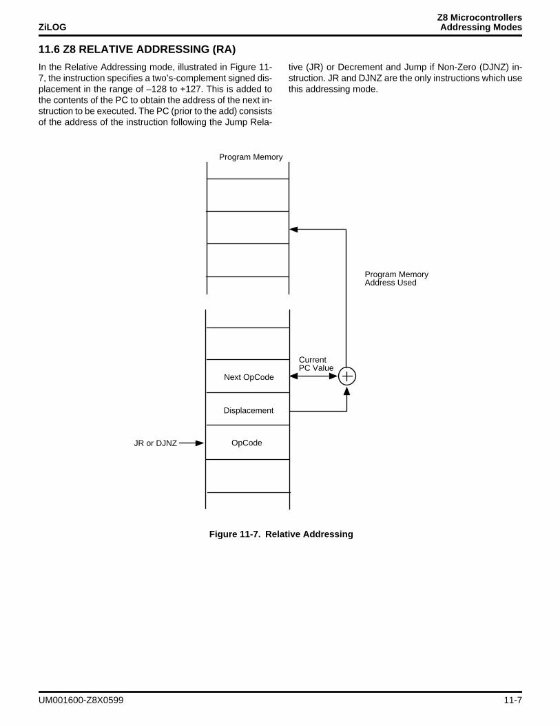
Z8 MicrocontrollersZiLOG Addressing Modes
11.6 Z8 RELATIVE ADDRESSING (RA)
In the Relative Addressing mode, illustrated in Figure 11-7, the instruction specifies a two’s-complement signed dis-placement in the range of –128 to +127. This is added tothe contents of the PC to obtain the address of the next in-struction to be executed. The PC (prior to the add) consistsof the address of the instruction following the Jump Rela-
tive (JR) or Decrement and Jump if Non-Zero (DJNZ) in-struction. JR and DJNZ are the only instructions which usethis addressing mode.
Figure 11-7. Relative Addressing
OpCode
Displacement
Next OpCode
Current
JR or DJNZ
Program Memory
Program MemoryAddress Used
PC Value
UM001600-Z8X0599 11-7
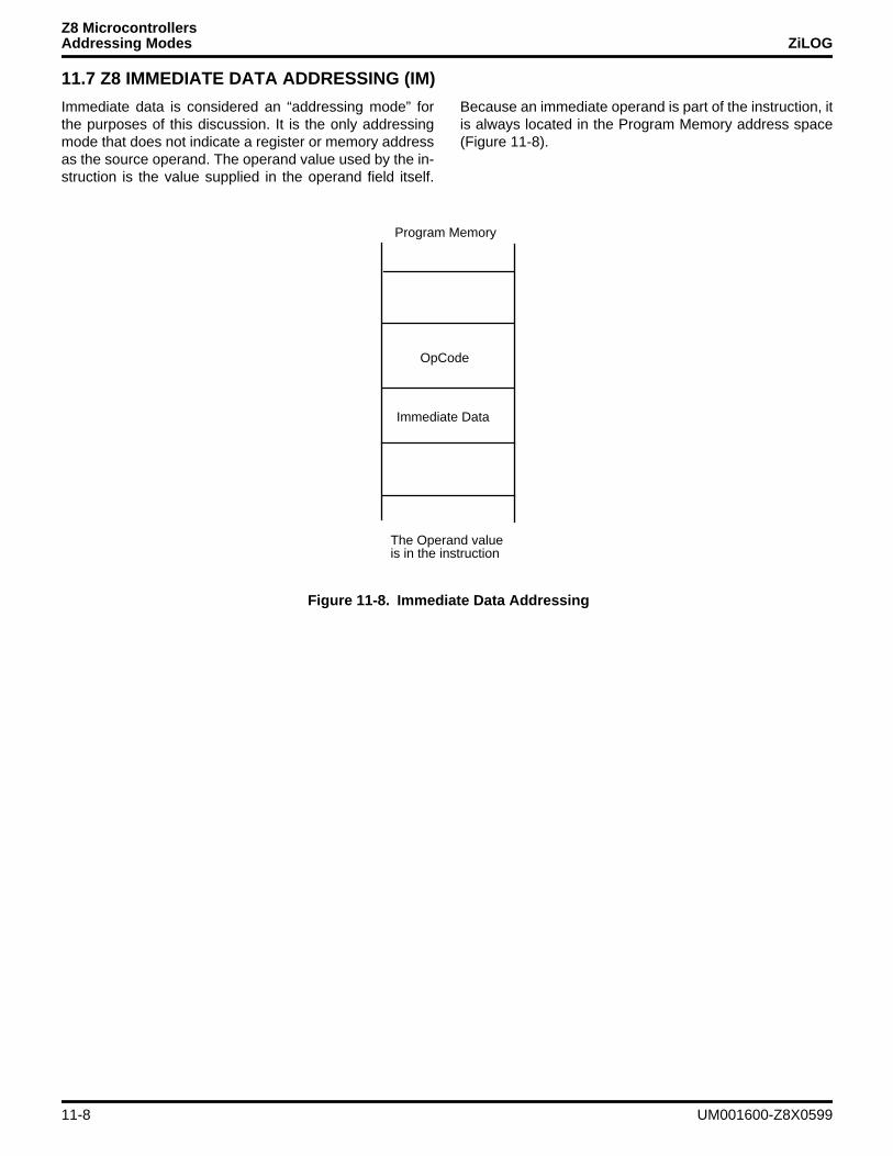
Z8 MicrocontrollersAddressing Modes ZiLOG
11.7 Z8 IMMEDIATE DATA ADDRESSING (IM)
Immediate data is considered an “addressing mode” forthe purposes of this discussion. It is the only addressingmode that does not indicate a register or memory addressas the source operand. The operand value used by the in-struction is the value supplied in the operand field itself.
Because an immediate operand is part of the instruction, itis always located in the Program Memory address space(Figure 11-8).
Figure 11-8. Immediate Data Addressing
OpCode
Immediate Data
Program Memory
The Operand valueis in the instruction
11-8 UM001600-Z8X0599
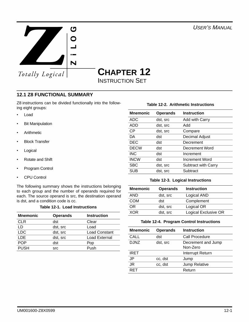
USER’S MANUAL
CHAPTER 12INSTRUCTION SET
12.1 Z8 FUNCTIONAL SUMMARY
Z8 instructions can be divided functionally into the follow-ing eight groups:
• Load
• Bit Manipulation
• Arithmetic
• Block Transfer
• Logical
• Rotate and Shift
• Program Control
• CPU Control
The following summary shows the instructions belongingto each group and the number of operands required foreach. The source operand is src, the destination operandis dst, and a condition code is cc.
Table 12-1. Load Instructions
Mnemonic Operands Instruction
CLR dst ClearLD dst, src LoadLDC dst, src Load ConstantLDE dst, src Load ExternalPOP dst PopPUSH src Push
Table 12-2. Arithmetic Instructions
Mnemonic Operands Instruction
ADC dst, src Add with CarryADD dst, src AddCP dst, src CompareDA dst Decimal AdjustDEC dst DecrementDECW dst Decrement WordINC dst IncrementINCW dst Increment WordSBC dst, src Subtract with CarrySUB dst, src Subtract
Table 12-3. Logical Instructions
Mnemonic Operands Instruction
AND dst, src Logical ANDCOM dst ComplementOR dst, src Logical ORXOR dst, src Logical Exclusive OR
Table 12-4. Program Control Instructions
Mnemonic Operands Instruction
CALL dst Call ProcedureDJNZ dst, src Decrement and Jump
Non-ZeroIRET Interrupt ReturnJP cc, dst JumpJR cc, dst Jump RelativeRET Return
UM001600-Z8X0599 12-1
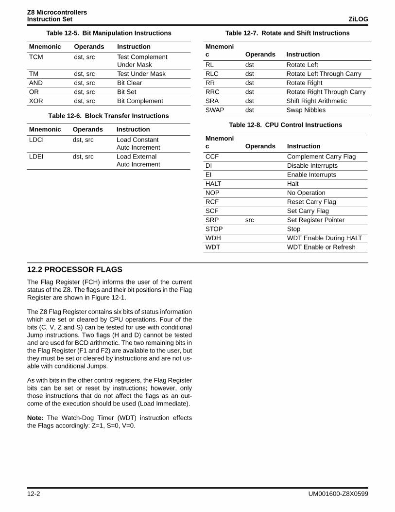
Z8 MicrocontrollersInstruction Set ZiLOG
12.2 PROCESSOR FLAGS
The Flag Register (FCH) informs the user of the currentstatus of the Z8. The flags and their bit positions in the FlagRegister are shown in Figure 12-1.
The Z8 Flag Register contains six bits of status informationwhich are set or cleared by CPU operations. Four of thebits (C, V, Z and S) can be tested for use with conditionalJump instructions. Two flags (H and D) cannot be testedand are used for BCD arithmetic. The two remaining bits inthe Flag Register (F1 and F2) are available to the user, butthey must be set or cleared by instructions and are not us-able with conditional Jumps.
As with bits in the other control registers, the Flag Registerbits can be set or reset by instructions; however, onlythose instructions that do not affect the flags as an out-come of the execution should be used (Load Immediate).
Note: The Watch-Dog Timer (WDT) instruction effectsthe Flags accordingly: Z=1, S=0, V=0.
Table 12-5. Bit Manipulation Instructions
Mnemonic Operands Instruction
TCM dst, src Test ComplementUnder Mask
TM dst, src Test Under MaskAND dst, src Bit ClearOR dst, src Bit SetXOR dst, src Bit Complement
Table 12-6. Block Transfer Instructions
Mnemonic Operands Instruction
LDCI dst, src Load ConstantAuto Increment
LDEI dst, src Load External Auto Increment
Table 12-7. Rotate and Shift Instructions
Mnemonic Operands Instruction
RL dst Rotate LeftRLC dst Rotate Left Through CarryRR dst Rotate RightRRC dst Rotate Right Through CarrySRA dst Shift Right ArithmeticSWAP dst Swap Nibbles
Table 12-8. CPU Control Instructions
Mnemonic Operands Instruction
CCF Complement Carry FlagDI Disable InterruptsEI Enable InterruptsHALT HaltNOP No OperationRCF Reset Carry FlagSCF Set Carry FlagSRP src Set Register PointerSTOP StopWDH WDT Enable During HALTWDT WDT Enable or Refresh
12-2 UM001600-Z8X0599
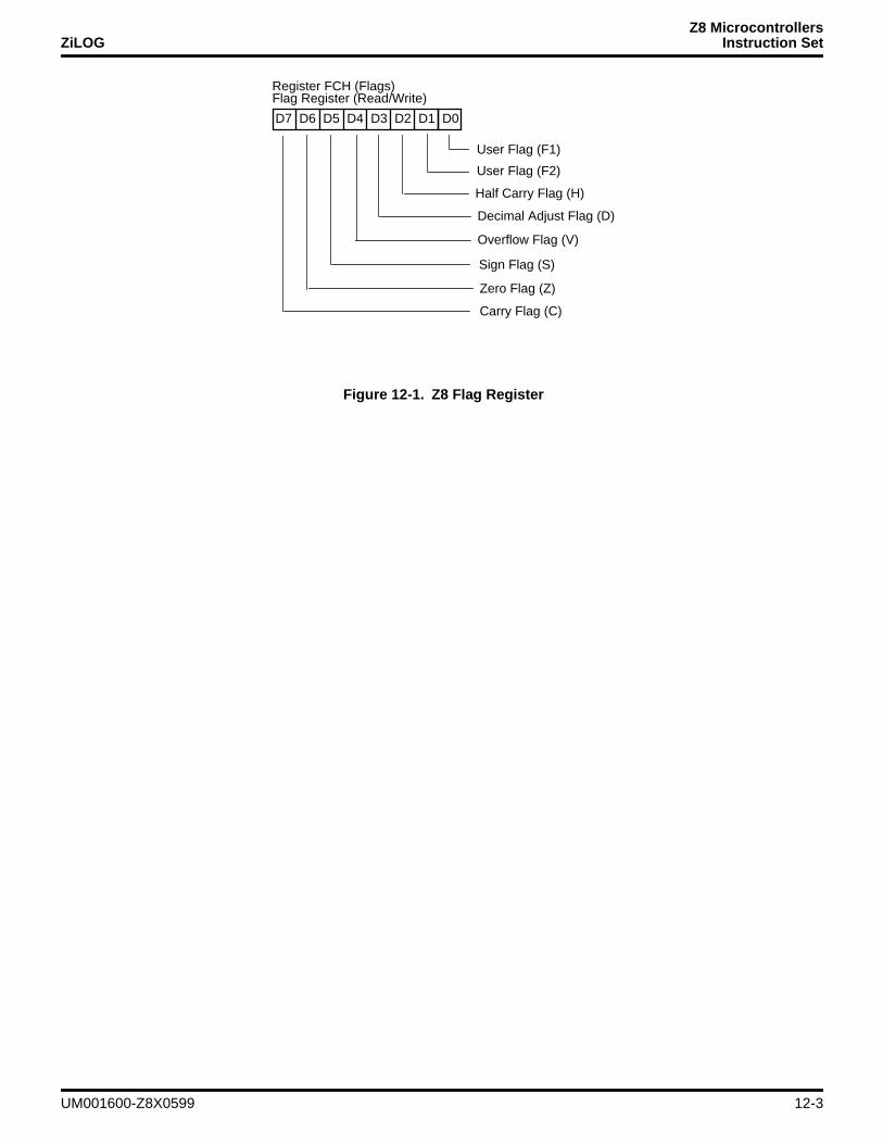
Z8 MicrocontrollersZiLOG Instruction Set
Figure 12-1. Z8 Flag Register
D7 D6 D5 D4 D3 D2 D1 D0
Flag Register (Read/Write)
Half Carry Flag (H)
User Flag (F1)
User Flag (F2)
Register FCH (Flags)
Overflow Flag (V)
Carry Flag (C)
Decimal Adjust Flag (D)
Zero Flag (Z)
Sign Flag (S)
UM001600-Z8X0599 12-3
Z8 MicrocontrollersInstruction Set ZiLOG
12.2.1 Carry Flag (C)The Carry Flag is set to 1 whenever the result of an arith-metic operation generates a carry or a borrow the high or-der bit 7. Otherwise, the Carry Flag is cleared to 0.
Following Rotate and Shift instructions, the Carry Flagcontains the last value shifted out of the specified register.
An instruction can set, reset, or complement the CarryFlag.
IRET may change the value of the Carry Flag when theFlag Register, saved in the Stack, is restored.
12.2.2 Zero Flag (Z)For arithmetic and logical operations, the Zero Flag is setto 1 if the result is zero. Otherwise, the Zero Flag is clearedto 0.
If the result of testing bits in a register is 00H, the Zero Flagis set to 1. Otherwise the Zero Flag is cleared to 0.
If the result of a Rotate or Shift operation is 00H, the ZeroFlag is set to 1. Otherwise, the Zero Flag is cleared to 0.
IRET changes the value of the Zero Flag when the FlagRegister saved in the Stack is restored. The WDT Instruc-tion sets the Zero Flag to a 1.
12.2.3 Sign Flag (S)The Sign Flag stores the value of the most significant bit ofa result following an arithmetic, logical, Rotate, or Shift op-eration.
When performing arithmetic operations on signed num-bers, binary two’s-complement notation is used to repre-sent and process information. A positive number is identi-fied by a 0 in the most significant bit position (bit 7);therefore, the Sign Flag is also 0.
A negative number is identified by a 1 in the most signifi-cant bit position (bit 7); therefore, the Sign Flag is also 1.
IRET changes the value of the Sign Flag when the FlagRegister saved in the Stack is restored.
12.2.4 Overflow Flag (V)For signed arithmetic, Rotate, and Shift operations, theOverflow Flag is set to 1 when the result is greater than themaximum possible number (>127) or less than the mini-mum possible number (<–128) that can be represented intwo’s-complement form. The Overflow Flag is set to 0 if nooverflow occurs.
Following logical operations the Overflow Flag is set to 0.
IRET changes the value of the Overflow Flag when theFlag Register saved in the Stack is restored.
12.2.5 Decimal Adjust Flag (D)The Decimal Adjust Flag is used for BCD arithmetic. Sincethe algorithm for correcting BCD operations is different foraddition and subtraction, this flag specifies what type of in-struction was last executed so that the subsequent Deci-mal Adjust (DA) operation can function properly. Normally,the Decimal Adjust Flag cannot be used as a test condi-tion.
After a subtraction, the Decimal Adjust Flag is set to 1. Fol-lowing an addition it is cleared to 0.
IRET changes the value of the Decimal Adjust Flag whenthe Flag Register saved in the Stack is restored.
12.2.6 Half Carry Flag (H)The Half Carry Flag is set to 1 whenever an addition gen-erates a carry bit 3 (Overflow) or a subtraction generates aborrow bit 3. The Half Carry Flag is used by the DecimalAdjust (DA) instruction to convert the binary result of a pre-vious addition or subtraction into the correct decimal(BCD) result. As in the case of the Decimal Adjust Flag, theuser does not normally access this flag.
IRET changes the value of the Half Carry Flag when theFlag Register saved in the Stack is restored.
12-4 UM001600-Z8X0599
Z8 MicrocontrollersZiLOG Instruction Set
12.3 CONDITION CODES
The C, Z, S, and V Flags control the operation of the ‘Con-ditional’ Jump instructions. Sixteen frequently useful func-tions of the flag settings are encoded in a 4-bit field calledthe condition code (cc), which forms bits 4-7 of the condi-tional instructions.
Condition codes and flag settings are summarized in Ta-bles 12-9, 12-10, and 12-11. Notation for the flags and howthey are affected are as follows:
Table 12-9. Z8 Flag Definitions
Flag Description
C Carry FlagZ Zero FlagS Sign FlagV Overflow FlagD Decimal Adjust FlagH Half Carry Flag
Table 12-10. Flag Settings Definitions
Symbol Definition
0 Cleared to 01 Set to 1* Set or cleared according to operation– UnaffectedX Undefined
Table 12-11. Condition Codes
Binary HEX Mnemonic Definition Flag Settings
0000 0 F Always False –1000 8 (blank) Always True –0111 7 C Carry C = 11111 F NC No Carry C = 00110 6 Z Zero Z = 11110 E NZ Non-Zero Z = 01101 D PL Plus S = 00101 5 Ml Minus S = 10100 4 OV Overflow V = 11100 C NOV No Overflow V = 00110 6 EQ Equal Z = 11110 E NE Not Equal Z = 01001 9 GE Greater Than or Equal (S XOR V) = 00001 1 LT Less Than (S XOR V) = 11010 A GT Greater Than (Z OR (S XOR V)) = 00010 2 LE Less Than or Equal (Z OR (S XOR V)) = 11111 F UGE Unsigned Greater Than or Equal C = 00111 7 ULT Unsigned Less Than C = 11011 B UGT Unsigned Greater Than (C = 0 AND Z = 0) = 10011 3 ULE Unsigned Less Than or Equal (C OR Z) = 1
UM001600-Z8X0599 12-5
Z8 MicrocontrollersInstruction Set ZiLOG
12.4 NOTATION AND BINARY ENCODING
In the detailed instruction descriptions that make up therest of this chapter, operands and status flags are repre-sented by a notational shorthand. Operands, condition
codes, address modes, and their notations are as follows(Table 12-12):
Table 12-12. Notational Shorthand
Notation Address Mode Operand Range *
cc Condition Code See condition codes r Working Register Rn n = 0 – 15R Register Reg Reg. represents a number in the range of 00H to FFH
orWorking Register Rn n = 0 – 15
RR Register Pair Reg Reg. represents an even number in the range of 00H to FEHorWorking Register Pair RRp p = 0, 2, 4, 6, 8, 10, 12, or 14
Ir Indirect Working Register @Rn n = 0 –15IR Indirect Register @Reg Reg. represents a number in the range of 00H to FFH
orIndirect Working Register @Rn n = 0– 15
Irr Indirect Working Register Pair
@RRp p = 0, 2, 4, 6, 8, 10, 12, or 14
IRR Indirect Register Pair @Reg Reg. represents an even number in the range 00H to FFHorWorking Register Pair @RRp p = 0, 2, 4, 6, 8, 10, 12, or 14
X Indexed Reg (Rn) Reg. represents a number in the range of 00H to FFH and n = 0 – 15
DA Direct Address Addrs Addrs. represents a number in the range of 00H to FFHRA Relative Address Addrs Addrs. represents a number in the range of +127 to –128
which is an offset relative to the address of the next instructionIM Immediate #Data Data is a number between 00H to FFH
*See the device product specification to determine the exact register file range available. The register file size varies by the devicetype.
12-6 UM001600-Z8X0599
Z8 MicrocontrollersZiLOG Instruction Set
Additional symbols used are:
Assignment of a value is indicated by the symbol “¨”. Forexample,
dst ¨ dst + src
indicates the source data is added to the destination dataand the result is stored in the destination location.
The notation 'addr(n)' is used to refer to bit'n' of a given lo-cation. For example,
dst (7)
refers to bit 7 of the destination operand.
12.4.1 Assembly Language SyntaxFor proper instruction execution, Z8 assembly languagesyntax requires ‘dst, src’ be specified, in that order. The fol-lowing instruction descriptions show the format of the ob-ject code produced by the assembler. This binary formatshould be followed by users who prefer manual programcoding or who intend to implement their own assembler.
Example : If the contents of registers 43H and 08H areadded and the result is stored in 43H, the assembly syntaxand resulting object code is:
In general, whenever an instruction format requires an 8-bit register address, that address can specify any registerlocation in the range 0 - 255 or a Working Register R0 -R15. If, in the above example, register 08H is a WorkingRegister, the assembly syntax and resulting object codewould be:
Note: See the device product specification to determinethe exact register file range available. The register file sizevaries by device type
Table 12-13. Additional Symbols
Symbol Definition
dst Destination Operandsrc Source Operand@ Indirect Address PrefixSP Stack PointerPC Program CounterFLAGS Flag Register (FCH)RP Register Pointer (FDH) IMR Interrupt Mask Register (FBH)# Immediate Operand Prefix% Hexadecimal Number PrefixH Hexadecimal Number SuffixB Binary Number SuffixOPC Opcode
ASM: ADD 43H, 08H (ADD dst, src)OBJ: 04 08 43 (OPC src, dst)
ASM: ADD 43H, 08H (ADD dst, src)OBJ: 04 08 43 (OPC src, dst)
UM001600-Z8X0599 12-7
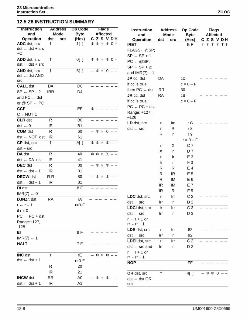
Z8 MicrocontrollersInstruction Set ZiLOG
12.5 Z8 INSTRUCTION SUMMARYInstruction
and Operation
AddressMode
Op CodeByte (Hex)
Flags Affected
dst src C Z S V D HADC dst, srcdst ← dst + src +C
† 1[ ] 0
ADD dst, srcdst ← dst + src
† 0[ ] 0
AND dst, srcdst ← dst AND src
† 5[ ] – 0 – –
CALL dst DA D6 – – – – – –SP ← SP – 2 IRR D4and PC ← dstor @ SP ← PCCCF EF – – – – –C ←NOT CCLR dst R B0 – – – – – –dst ← 0 IR B1COM dst R 60 – 0 – –dst ← NOT dst IR 61CP dst, src † A[ ] – –dst − srcDA dst R 40 X – –dst ← DA dst IR 41DEC dst R 00 – – –dst ← dst – 1 IR 01DECW dst R R 80 – – –dst ← dst – 1 IR 81DI dst 8 F – – – – – –IMR(7) ← 0DJNZr, dst RA rA – – – – – –r ← r – 1 r=0-Fif r ≠ 0PC ← PC + dstRange:+127,-128EI 9 F – – – – – –IMR(7) ← 1HALT 7 F – – – – – –
INC dstdst ← dst + 1
r rE – – –r=0-F
R 20IR 21
INCW dst RR A0 – – –dst ← dst + 1 IR A1
Instructionand
Operation
AddressMode
Op CodeByte (Hex)
Flags Affected
dst src C Z S V D HIRET B F
FLAGS←@SP;SP ← SP + 1PC ← @SP;SP ← SP + 2;and IMR(7) – 1JP cc, dst DA cD – – – – – –if cc is true, c = 0 – Fthen PC ← dst IRR 30JR cc, dst RA cB – – – – – –if cc is true, c = 0 – FPC ← PC + dstRange: +127, –128LD dst, src r Im r C – – – – – –dst ← src r R r 8
R r r 9r = 0 – F
r X C 7X r D 7r Ir E 3Ir r F 3R R E 4R IR E 5R IM E 6IR IM E 7IR R F 5
LDC dst, src r Irr C 2 – – – – – –dst ← src lrr r D 2LDCI dst, src Ir Irr C 3 – – – – – –dst ← src lrr r D 3r ← r + 1 orrr ←rr + 1LDE dst, src r Irr 82 – – – – – –dst ← src lrr r 92LDEI dst, src r Irr C 2 – – – – – –dst ← src and lrr r D 2r ← r + 1 orrr ←rr + 1NOP FF – – – – – –
OR dst, src † 4[ ] – 0 – –dst ← dst OR src
12-8 UM001600-Z8X0599
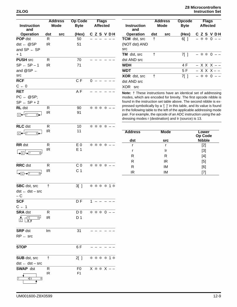
Z8 MicrocontrollersZiLOG Instruction Set
InstructionAddress
ModeOp Code
ByteFlags
Affectedand
Operation dst src (Hex) C Z S V D HPOP dst R 50 – – – – – –dst ← @SP IR 51and SP ← SP + 1PUSH src R 70 – – – – – –SP ← SP – 1 IR 71and @SP ← srcRCF C F 0 – – – – –C ← 0RET A F – – – – – –PC ← @SP;SP ← SP + 2RL dst R
IR9091
– –
RLC dst RIR
1011
– –
RR dst RIR
E 0E 1
– –
RRC dst R C 0 – –IR C 1
SBC dst, src † 3[ ] 1
dst ← dst – src – CSCF D F 1 – – – – –C ← 1SRA dst R D 0 0 – –
IR D 1
SRP dst Im 31 – – – – – –RP ← src
STOP 6 F – – – – – –
SUB dst, src † 2[ ] 1
dst ← dst – srcSWAP dst R
IRF0F1
X X – –
C 7 0
C 7 0
C 7 0
C 7 0
C7 0
7 4 3 0
InstructionAddress
ModeOpcode
ByteFlags
Affectedand
Operation dst src (Hex) C Z S V D HTCM dst, src † 6[ ] – 0 – –(NOT dst) AND srcTM dst, src † 7[ ] – 0 – –dst AND srcWDH 4 F – X X X – –WDT 5 F – X X X – –XOR dst, src † 7[ ] – 0 – –dst AND srcXOR src
Note: † These instructions have an identical set of addressingmodes, which are encoded for brevity. The first opcode nibble isfound in the instruction set table above. The second nibble is ex-pressed symbolically by a ‘[ ]’ in this table, and its value is foundin the following table to the left of the applicable addressing modepair. For example, the opcode of an ADC instruction using the ad-dressing modes r (destination) and Ir (source) is 13.
Address Mode Lower
dst srcOp Code
Nibbler r [2]r Ir [3]R R [4]R IR [5]R IM [6]IR IM [7]
UM001600-Z8X0599 12-9
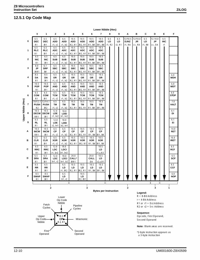
Z8 MicrocontrollersInstruction Set ZiLOG
12.5.1 Op Code Map
10.5CP
R , R1
6.5DECR1
6.5DECIR1
6.5ADDr1, r2
6.5ADDr1, Ir2
10.5ADD
R2, R1
10.5ADD
IR2, R1
10.5ADD
R1, IM
10.5ADD
IR1, IM
0 1 2 3 4 5 6 7 8 9 A B C D E F
0
1
2
3
4
5
6
7
8
9
A
B
C
D
E
F
Lower Nibble (Hex)
Bytes per Instruction2 3 2 3 1
6.5RLCR1
6.5RLCIR1
6.5ADCr1, r2
6.5ADCr1, Ir2
10.5ADC
R2, R1
10.5ADC
IR2, R1
10.5ADC
R1, IM
10.5ADC
IR1, IM6.5INCR1
6.5INCIR1
6.5SUBr1, r2
6.5SUBr1, Ir2
10.5SUB
R2, R1
10.5SUB
IR2, R1
10.5SUB
R1, IM
10.5SUB
IR1, IM
10.5DECWRR1
10.5DECW
IR16.5RLR1
6.5RLIR1
10.5INCWRR1
10.5INCW
IR1
6.5CP
r1, r2
6.5CP
r1, Ir2
10.5CP
R2, R1
10.5CP
IR2, R1
10.5CP
R1, IM
10.5CP
IR1, IM6.5
CLRR1
6.5CLRIR1
6.5XORr1, r2
6.5XORr1, Ir2
10.5XOR
R2, R1
10.5XOR
IR2, R1
10.5XOR
R1, IM
10.5XOR
IR1, IM6.5
RRCR1
6.5RRCIR1
12.0LDC
r1, Irr2
18.0LDCI
Ir1, Irr2
10.5LD
r1,x,R26.5
SRAR1
6.5SRAIR1
20.0CALL*IRR1
20.0CALL
DA
10.5LD
r2,x,R16.5RRR1
6.5RRIR1
6.5LD
r1, IR2
10.5LD
R2, R1
10.5LD
IR2, R1
10.5LD
R1, IM
10.5LD
IR1, IM8.5
SWAPR1
8.5SWAP
IR1
6.5LD
Ir1, r2
10.5LD
R2, IR1
6.5LD
r1, R2
6.5LD
r2, R1
12/10.5DJNZr1, RA
12/10.0JR
cc, RA
6.5LD
r1, IM
12.10.0JP
cc, DA
6.5INCr1
6.0STOP
7.0HALT
6.1DI
6.1EI
14.0RET
16.0IRET
6.5RCF
6.5SCF
6.5CCF
6.0NOP
2
4
A
LowerOp CodeNibble
PipelineCycles
Mnemonic
SecondOperand
FetchCycles
UpperOp Code
Nibble
FirstOperand
Legend:R = 8-Bit Addressr = 4-Bit AddressR1 or r1 = Dst AddressR2 or r2 = Src Address
Sequence:Opcode, First Operand,Second Operand
Note: Blank areas are reserved.
*2-byte instruction appears as a 3-byte instruction
8.0JP
IRR1
6.1SRPIM
6.5SBCr1, r2
6.5SBCr1, Ir2
10.5SBC
R2, R1
10.5SBC
IR2, R1
10.5SBC
R1, IM
10.5SBC
IR1, IM8.5DAR1
8.5DAIR1
6.5OR
r1, r2
6.5OR
r1, Ir2
10.5OR
R2, R1
10.5OR
IR2, R1
10.5OR
R1, IM
10.5OR
IR1, IM10.5POPR1
10.5POPIR1
6.5ANDr1, r2
6.5ANDr1, Ir2
10.5AND
R2, R1
10.5AND
IR2, R1
10.5AND
R1, IM
10.5AND
IR1, IM6.5
COMR1
6.5COMIR1
6.5TCMr1, r2
6.5TCMr1, Ir2
10.5TCM
R2, R1
10.5TCM
IR2, R1
10.5TCM
R1, IM
10.5TCM
IR1, IM10/12.1PUSH
R2
12/14.1PUSH
IR2
6.5TM
r1, r2
6.5TM
r1, Ir2
10.5TM
R2, R1
10.5TM
IR2, R1
10.5TM
R1, IM
10.5TM
IR1, IM
6.0WDT
6.0WDH
Upp
er N
ibbl
e (H
ex)
12.0LDC
lrr1, r2
18.0LDCI
lrr1, Ir2
12.0LDE
r1, lrr2
18.0LDEI
lr1, lrr212.0LDE
r2, lrr1
18.0LDEI
lr2, lrr1
12-10 UM001600-Z8X0599
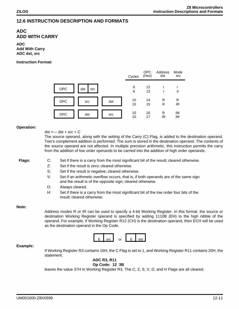
Z8 MicrocontrollersZiLOG Instruction Descriptions and Formats
12.6 INSTRUCTION DESCRIPTION AND FORMATS
ADCADD WITH CARRY
ADCAdd With CarryADC dst, src
Instruction Format:
Operation: dst <— dst + src + CThe source operand, along with the setting of the Carry (C) Flag, is added to the destination operand.Two’s complement addition is performed. The sum is stored in the destination operand. The contents ofthe source operand are not affected. In multiple precision arithmetic, this instruction permits the carryfrom the addition of low order operands to be carried into the addition of high order operands.
Note:Address modes R or IR can be used to specify a 4-bit Working Register. In this format, the source ordestination Working Register operand is specified by adding 1110B (EH) to the high nibble of theoperand. For example, if Working Register R12 (CH) is the destination operand, then ECH will be usedas the destination operand in the Op Code.
Example:If Working Register R3 contains 16H, the C Flag is set to 1, and Working Register R11 contains 20H, thestatement:
ADC R3, R11Op Code: 12 3B
leaves the value 37H in Working Register R3. The C, Z, S, V, D, and H Flags are all cleared.
Flags: C: Set if there is a carry from the most significant bit of the result; cleared otherwise.Z: Set if the result is zero; cleared otherwise.S: Set if the result is negative; cleared otherwise.V: Set if an arithmetic overflow occurs, that is, if both operands are of the same sign
and the result is of the opposite sign; cleared otherwise.D: Always cleared.H: Set if there is a carry from the most significant bit of the low order four bits of the
result; cleared otherwise.
dst srcOPC
OPC
OPC
src
dst
dst
src
6
CyclesOPC(Hex)
Addressdst
Modesrc
12 r r6 13 r Ir
10 14 R R10 15 R IR
10 16 R IM10 17 IR IM
E src E dstor
UM001600-Z8X0599 12-11
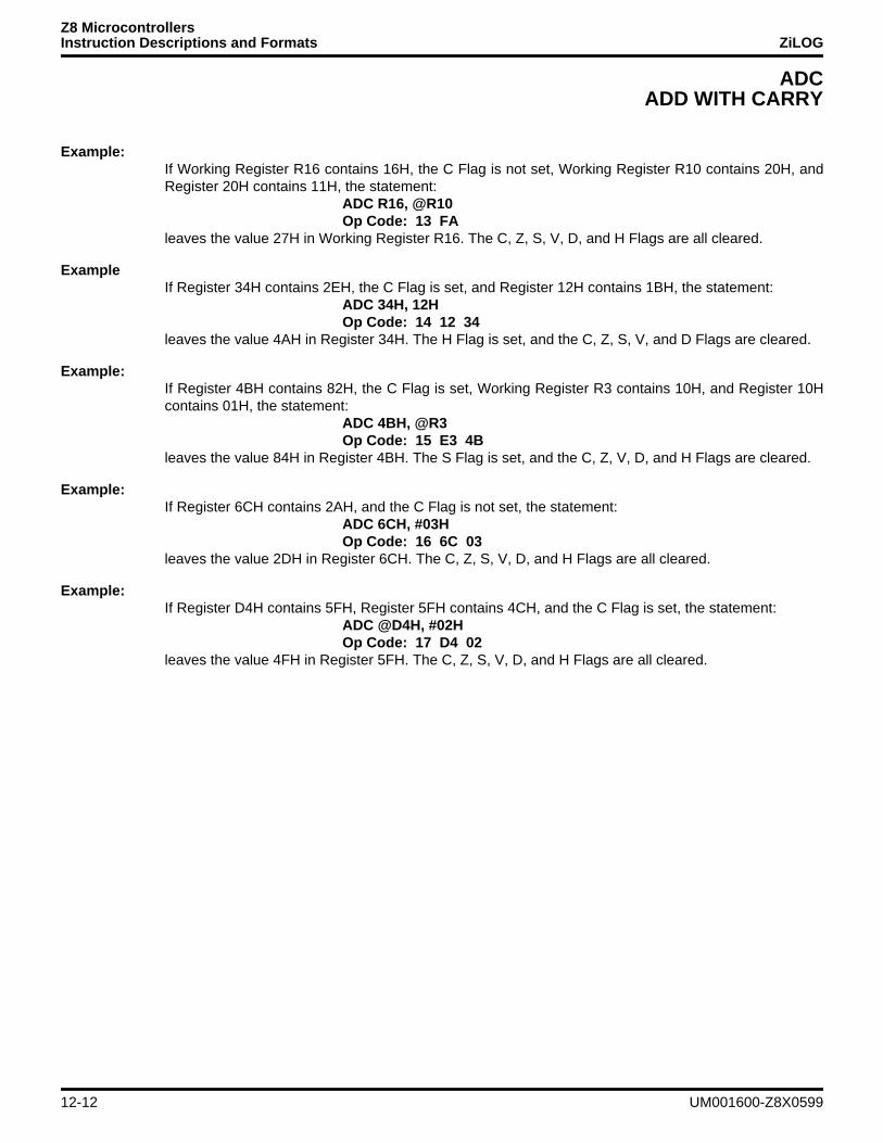
Z8 MicrocontrollersInstruction Descriptions and Formats ZiLOG
ADCADD WITH CARRY
Example: If Working Register R16 contains 16H, the C Flag is not set, Working Register R10 contains 20H, andRegister 20H contains 11H, the statement:
ADC R16, @R10Op Code: 13 FA
leaves the value 27H in Working Register R16. The C, Z, S, V, D, and H Flags are all cleared.
ExampleIf Register 34H contains 2EH, the C Flag is set, and Register 12H contains 1BH, the statement:
ADC 34H, 12HOp Code: 14 12 34
leaves the value 4AH in Register 34H. The H Flag is set, and the C, Z, S, V, and D Flags are cleared.
Example:If Register 4BH contains 82H, the C Flag is set, Working Register R3 contains 10H, and Register 10Hcontains 01H, the statement:
ADC 4BH, @R3Op Code: 15 E3 4B
leaves the value 84H in Register 4BH. The S Flag is set, and the C, Z, V, D, and H Flags are cleared.
Example:If Register 6CH contains 2AH, and the C Flag is not set, the statement:
ADC 6CH, #03HOp Code: 16 6C 03
leaves the value 2DH in Register 6CH. The C, Z, S, V, D, and H Flags are all cleared.
Example:If Register D4H contains 5FH, Register 5FH contains 4CH, and the C Flag is set, the statement:
ADC @D4H, #02HOp Code: 17 D4 02
leaves the value 4FH in Register 5FH. The C, Z, S, V, D, and H Flags are all cleared.
12-12 UM001600-Z8X0599
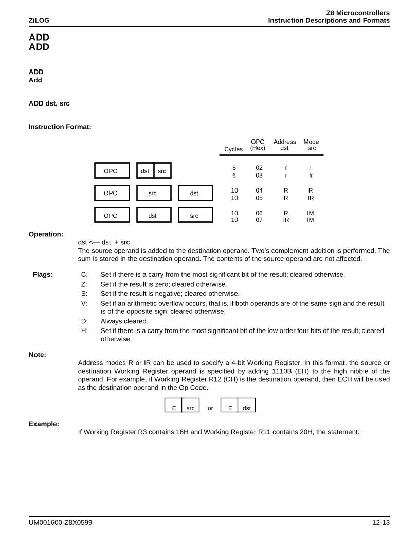
Z8 MicrocontrollersZiLOG Instruction Descriptions and Formats
ADDADD
ADDAdd
ADD dst, src
Instruction Format:
Operation:dst <— dst + src The source operand is added to the destination operand. Two’s complement addition is performed. Thesum is stored in the destination operand. The contents of the source operand are not affected.
Note:Address modes R or IR can be used to specify a 4-bit Working Register. In this format, the source ordestination Working Register operand is specified by adding 1110B (EH) to the high nibble of theoperand. For example, if Working Register R12 (CH) is the destination operand, then ECH will be usedas the destination operand in the Op Code.
Example:If Working Register R3 contains 16H and Working Register R11 contains 20H, the statement:
dst srcOPC
OPC
OPC
src
dst
dst
src
6
CyclesOPC(Hex)
Addressdst
Modesrc
02 r r6 03 r Ir
10 04 R R10 05 R IR
10 06 R IM10 07 IR IM
Flags : C: Set if there is a carry from the most significant bit of the result; cleared otherwise.Z: Set if the result is zero; cleared otherwise.S: Set if the result is negative; cleared otherwise.V: Set if an arithmetic overflow occurs, that is, if both operands are of the same sign and the result
is of the opposite sign; cleared otherwise.D: Always cleared.H: Set if there is a carry from the most significant bit of the low order four bits of the result; cleared
otherwise.
E src E dstor
UM001600-Z8X0599 12-13
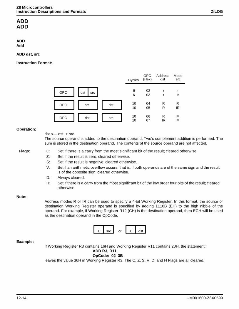
Z8 MicrocontrollersInstruction Descriptions and Formats ZiLOG
ADDADD
ADDAdd
ADD dst, src
Instruction Format:
Operation:dst <— dst + src The source operand is added to the destination operand. Two’s complement addition is performed. Thesum is stored in the destination operand. The contents of the source operand are not affected.
Note:Address modes R or IR can be used to specify a 4-bit Working Register. In this format, the source ordestination Working Register operand is specified by adding 1110B (EH) to the high nibble of theoperand. For example, if Working Register R12 (CH) is the destination operand, then ECH will be usedas the destination operand in the OpCode.
Example:If Working Register R3 contains 16H and Working Register R11 contains 20H, the statement:
ADD R3, R11OpCode: 02 3B
leaves the value 36H in Working Register R3. The C, Z, S, V, D, and H Flags are all cleared.
Flags : C: Set if there is a carry from the most significant bit of the result; cleared otherwise.Z: Set if the result is zero; cleared otherwise.S: Set if the result is negative; cleared otherwise.V: Set if an arithmetic overflow occurs, that is, if both operands are of the same sign and the result
is of the opposite sign; cleared otherwise.D: Always cleared.H: Set if there is a carry from the most significant bit of the low order four bits of the result; cleared
otherwise.
dst srcOPC
OPC
OPC
src
dst
dst
src
6
CyclesOPC(Hex)
Addressdst
Modesrc
02 r r6 03 r Ir
10 04 R R10 05 R IR
10 06 R IM10 07 IR IM
E src E dstor
12-14 UM001600-Z8X0599

Z8 MicrocontrollersZiLOG Instruction Descriptions and Formats
ADDADD
Example:If Working Register R16 contains 16H, Working Register R10 contains 20H, and Register 20H contains11H, the statement:
ADD R16, @R10Op Code: 03 FA
leaves the value 27H in Working Register R16. The C, Z, S, V, D, and H Flags are all cleared.
Example:If Register 34H contains 2EH and Register 12H contains 1BH, the statement:
ADD 34H, 12HOp Code: 04 12 34
leaves the value 49H in Register 34H. The H Flag is set, and the C, Z, S, V, and D Flags are cleared.
ExampleIf Register 4BH contains 82H, Working Register R3 contains 10H, and Register 10H contains 01H, thestatement:
ADD 3EH, @R3Op Code: 05 E3 4B
leaves the value 83H in Register 4BH. The S Flag is set, and the C, Z, V, D, and H Flags are cleared.
Example:If Register 6CH contains 2AH, the statement:
ADD 6CH, #03HOp Code: 06 6C 03
leaves the value 2DH in Register 6CH. The C, Z, S, V, D, and H Flags are all cleared.
Example:If Register D4H contains 5FH and Register 5FH contains 4CH, the statement:
ADD @D4H, #02HOp Code: 07 D4 02
leaves the value 4EH in Register 5FH. The C, Z, S, V, D, and H Flags are all cleared.
UM001600-Z8X0599 12-15
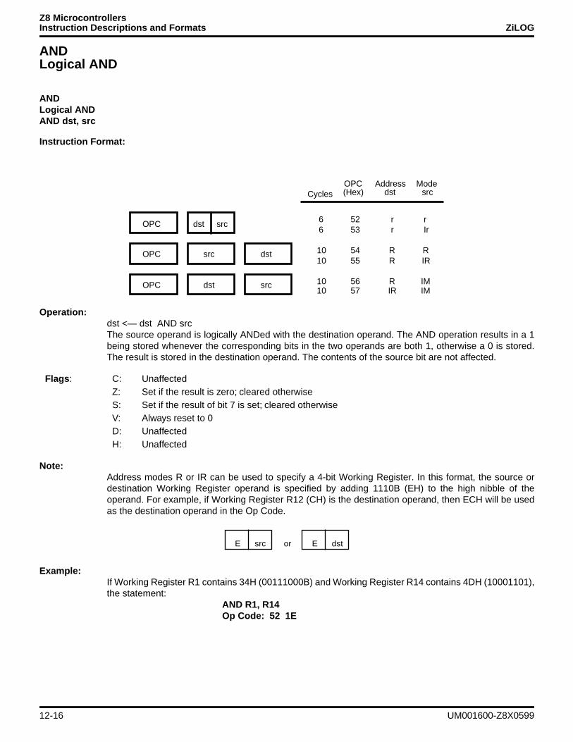
Z8 MicrocontrollersInstruction Descriptions and Formats ZiLOG
ANDLogical AND
ANDLogical ANDAND dst, src
Instruction Format:
Operation:dst <— dst AND src The source operand is logically ANDed with the destination operand. The AND operation results in a 1being stored whenever the corresponding bits in the two operands are both 1, otherwise a 0 is stored.The result is stored in the destination operand. The contents of the source bit are not affected.
Note:Address modes R or IR can be used to specify a 4-bit Working Register. In this format, the source ordestination Working Register operand is specified by adding 1110B (EH) to the high nibble of theoperand. For example, if Working Register R12 (CH) is the destination operand, then ECH will be usedas the destination operand in the Op Code.
Example:If Working Register R1 contains 34H (00111000B) and Working Register R14 contains 4DH (10001101),the statement:
AND R1, R14Op Code: 52 1E
dst srcOPC
OPC
OPC
src
dst
dst
src
6
CyclesOPC(Hex)
Addressdst
Modesrc
52 r r6 53 r Ir
10 54 R R10 55 R IR
10 56 R IM10 57 IR IM
Flags : C: UnaffectedZ: Set if the result is zero; cleared otherwiseS: Set if the result of bit 7 is set; cleared otherwiseV: Always reset to 0D: UnaffectedH: Unaffected
E src E dstor
12-16 UM001600-Z8X0599
Z8 MicrocontrollersZiLOG Instruction Descriptions and Formats
ADDADD
ADDAdd:
ADD dst, src:
Instruction Format:
Operation: dst <— dst + src The source operand is added to the destination operand. Two’s complement addition is performed. Thesum is stored in the destination operand. The contents of the source operand are not affected.
Note: Address modes R or IR can be used to specify a 4-bit Working Register. In this format, the source ordestination Working Register operand is specified by adding 1110B (EH) to the high nibble of theoperand. For example, if Working Register R12 (CH) is the destination operand, then ECH will be usedas the destination operand in the OpCode.
Example: If Working Register R3 contains 16H and Working Register R11 contains 20H, the statement:ADD R3, R11OpCode: 02 3B
leaves the value 36H in Working Register R3. The C, Z, S, V, D, and H Flags are all cleared.
dst srcOPC
OPC
OPC
src
dst
dst
src
6
CyclesOPC(Hex)
Addressdst
Modesrc
02 r r6 03 r Ir
10 04 R R10 05 R IR
10 06 R IM10 07 IR IM
Flags : C: Set if there is a carry from the most significant bit of the result; cleared otherwise.Z: Set if the result is zero; cleared otherwise.S: Set if the result is negative; cleared otherwise.V: Set if an arithmetic overflow occurs, that is, if both operands are of the same sign and the result
is of the opposite sign; cleared otherwise.D: Always cleared.H: Set if there is a carry from the most significant bit of the low order four bits of the result; cleared
otherwise.
E src E dstor
UM001600-Z8X0599 12-17
Z8 MicrocontrollersInstruction Descriptions and Formats ZiLOG
ANDLogical AND
Example:If Working Register R4 contains F9H (11111001B), Working Register R13 contains 7BH, and Register7BH contains 6AH (01101010B), the statement:
AND R4, @R13Op Code: 53 4D
leaves the value 68H (01101000B) in Working Register R4. The Z, V, and S Flags are cleared.
Example:If Register 3AH contains the value F5H (11110101B) and Register 42H contains the value 0AH(00001010), the statement:
AND 3AH, 42HOp Code: 54 42 3A
leaves the value 00H (00000000B) in Register 3AH. The Z Flag is set, and the V and S Flags are cleared.
Example:If Working Register R5 contains F0H (11110000B), Register 45H contains 3AH, and Register 3AHcontains 7FH (01111111B), the statement:
AND R5, @45HOp Code: 55 45 E5
leaves the value 70H (01110000B) in Working Register R5. The Z, V, and S Flags are cleared.
Example:If Register 7AH contains the value F7H (11110111B), the statement:
AND 7AH, #F0HOp Code: 56 7A F0
leaves the value F0H (11110000B) in Register 7AH. The S Flag is set, and the Z and V Flags are cleared.
Example:If Working Register R3 contains the value 3EH and Register 3EH contains the value ECH (11101100B),the statement:
AND @R3, #05HOp Code: 57 E3 05
leaves the value 04H (00000100B) in Register 3EH. The Z, V, and S Flags are cleared.
12-18 UM001600-Z8X0599
Z8 MicrocontrollersZiLOG Instruction Descriptions and Formats
CALLCALL PROCEDURE
CALLCall ProcedureCALL dst
Instruction Format:
Operation:SP <— SP - 2@SP <— PCPC <— dstThe Stack pointer is decremented by two, the current contents of the Program Counter (PC) (address ofthe first instruction following the CALL instruction) are pushed onto the top of the Stack, and the specifieddestination address is then loaded into the PC. The PC now points to the first instruction of the procedure.At the end of the procedure a RET (return) instruction can be used to return to the original program flow.RET will pop the top of the Stack and replace the original value into the PC.
Note:Address mode IRR can be used to specify a 4-bit Working Register Pair. In this format, the destinationWorking Register Pair operand is specified by adding 1110B (EH) to the high nibble of the operand. Forexample, if Working Register Pair RR12 (CH) is the destination operand, then ECH will be used as thedestination operand in the Op Code.
dstOPC
OPC dst
20
CyclesOPC(Hex)
Address Modedst
D6 DA
20 D4 IRR
Flags: C: UnaffectedZ: UnaffectedS: UnaffectedV: UnaffectedD: UnaffectedH: Unaffected
E dst
UM001600-Z8X0599 12-19
Z8 MicrocontrollersInstruction Descriptions and Formats ZiLOG
CALLCall Procedure
Example:If the contents of the PC are 1A47H and the contents of the SP (Registers FEH and FFH) are 3002H, thestatement:
CALL 3521HOp Code: D6 35 21
causes the SP to be decremented to 3000H, 1A4AH (the address following the CALL instruction) to bestored in external data memory 3000 and 3001H, and the PC to be loaded with 3521H. The PC nowpoints to the address of the first statement in the procedure to be executed.
Example:If the contents of the PC are 1A47H, the contents of the SP (Register FFH) are 72H, the contents ofRegister A4H are 34H, and the contents of Register Pair 34H are 3521H, the statement:
CALL @A4HOp Code: D4 A4
causes the SP to be decremented to 70H, 1A4AH (the address following the CALL instruction) to bestored in R70H and 71H, and the PC to be loaded with 3521H. The PC now points to the address of thefirst statement in the procedure to be executed.
12-20 UM001600-Z8X0599
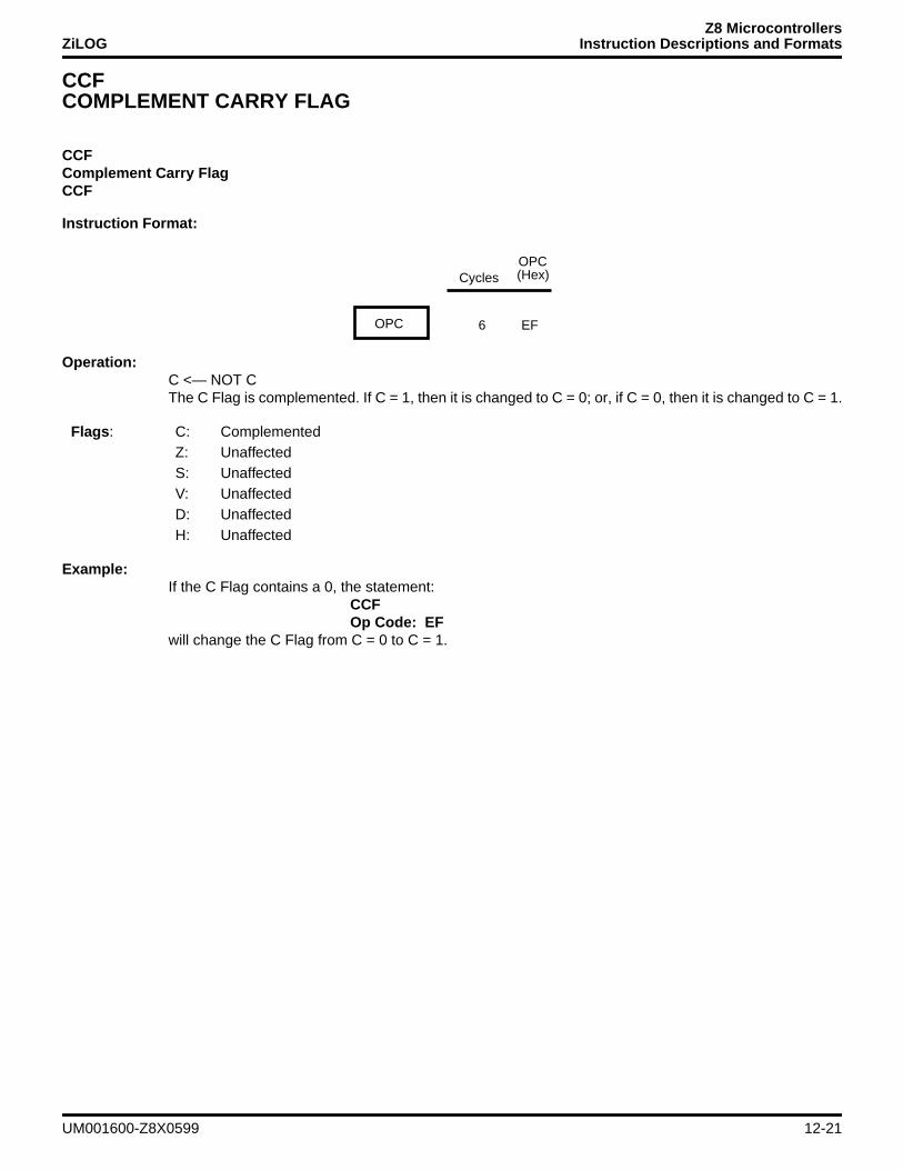
Z8 MicrocontrollersZiLOG Instruction Descriptions and Formats
CCFCOMPLEMENT CARRY FLAG
CCFComplement Carry FlagCCF
Instruction Format:
Operation:C <— NOT CThe C Flag is complemented. If C = 1, then it is changed to C = 0; or, if C = 0, then it is changed to C = 1.
Example:If the C Flag contains a 0, the statement:
CCFOp Code: EF
will change the C Flag from C = 0 to C = 1.
OPC 6
CyclesOPC(Hex)
EF
Flags : C: ComplementedZ: UnaffectedS: UnaffectedV: UnaffectedD: UnaffectedH: Unaffected
UM001600-Z8X0599 12-21
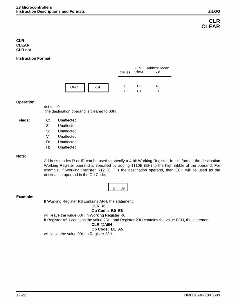
Z8 MicrocontrollersInstruction Descriptions and Formats ZiLOG
CLRCLEAR
CLRCLEARCLR dst
Instruction Format:
Operation:dst <— 0The destination operand is cleared to 00H.
Note:Address modes R or IR can be used to specify a 4-bit Working Register. In this format, the destinationWorking Register operand is specified by adding 1110B (EH) to the high nibble of the operand. Forexample, if Working Register R12 (CH) is the destination operand, then ECH will be used as thedestination operand in the Op Code.
Example:If Working Register R6 contains AFH, the statement:
CLR R6Op Code: B0 E6
will leave the value 00H in Working Register R6.If Register A5H contains the value 23H, and Register 23H contains the value FCH, the statement:
CLR @A5HOp Code: B1 A5
will leave the value 00H in Register 23H.
OPC dst 6
CyclesOPC(Hex)
Address Modedst
B0 R6 B1 IR
Flags: C: UnaffectedZ: UnaffectedS: UnaffectedV: UnaffectedD: UnaffectedH: Unaffected
E dst
12-22 UM001600-Z8X0599
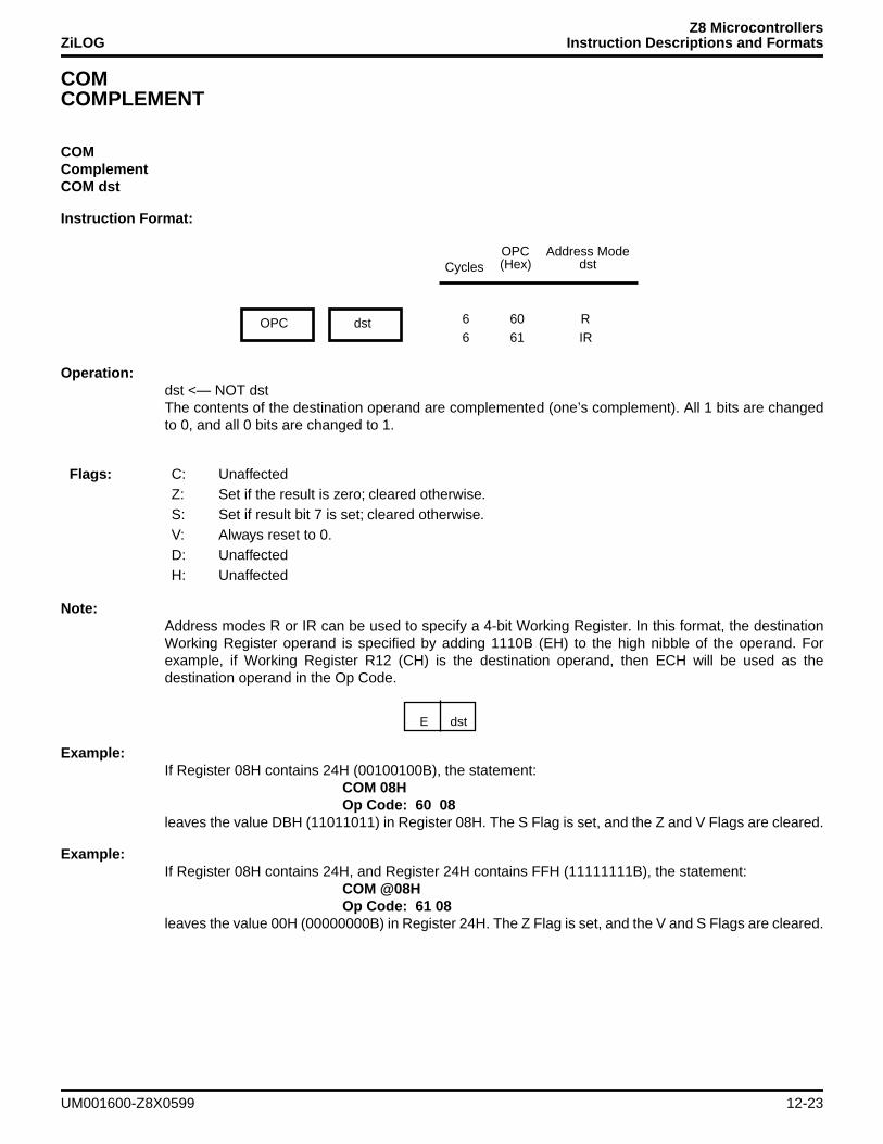
Z8 MicrocontrollersZiLOG Instruction Descriptions and Formats
COMCOMPLEMENT
COMComplementCOM dst
Instruction Format:
Operation:dst <— NOT dstThe contents of the destination operand are complemented (one’s complement). All 1 bits are changedto 0, and all 0 bits are changed to 1.
Note:Address modes R or IR can be used to specify a 4-bit Working Register. In this format, the destinationWorking Register operand is specified by adding 1110B (EH) to the high nibble of the operand. Forexample, if Working Register R12 (CH) is the destination operand, then ECH will be used as thedestination operand in the Op Code.
Example:If Register 08H contains 24H (00100100B), the statement:
COM 08HOp Code: 60 08
leaves the value DBH (11011011) in Register 08H. The S Flag is set, and the Z and V Flags are cleared.
Example:If Register 08H contains 24H, and Register 24H contains FFH (11111111B), the statement:
COM @08HOp Code: 61 08
leaves the value 00H (00000000B) in Register 24H. The Z Flag is set, and the V and S Flags are cleared.
OPC dst 6
CyclesOPC(Hex)
Address Modedst
60 R6 61 IR
Flags: C: UnaffectedZ: Set if the result is zero; cleared otherwise.S: Set if result bit 7 is set; cleared otherwise.V: Always reset to 0.D: UnaffectedH: Unaffected
E dst
UM001600-Z8X0599 12-23
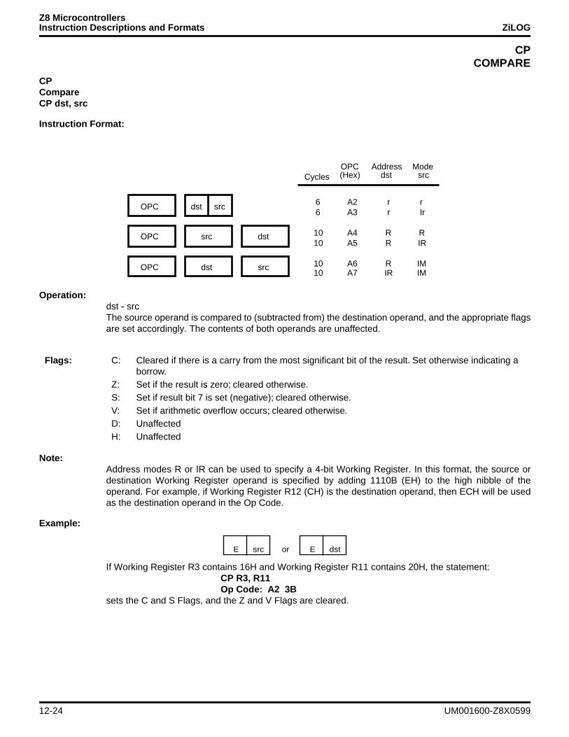
Z8 MicrocontrollersInstruction Descriptions and Formats ZiLOG
CPCOMPARE
CPCompareCP dst, src
Instruction Format:
Operation:dst - srcThe source operand is compared to (subtracted from) the destination operand, and the appropriate flagsare set accordingly. The contents of both operands are unaffected.
Note:Address modes R or IR can be used to specify a 4-bit Working Register. In this format, the source ordestination Working Register operand is specified by adding 1110B (EH) to the high nibble of theoperand. For example, if Working Register R12 (CH) is the destination operand, then ECH will be usedas the destination operand in the Op Code.
Example:
If Working Register R3 contains 16H and Working Register R11 contains 20H, the statement:CP R3, R11Op Code: A2 3B
sets the C and S Flags, and the Z and V Flags are cleared.
dst srcOPC
OPC
OPC
src
dst
dst
src
6
CyclesOPC(Hex)
Addressdst
Modesrc
A2 r r6 A3 r Ir
10 A4 R R10 A5 R IR
10 A6 R IM10 A7 IR IM
Flags: C: Cleared if there is a carry from the most significant bit of the result. Set otherwise indicating a borrow.
Z: Set if the result is zero; cleared otherwise.S: Set if result bit 7 is set (negative); cleared otherwise.V: Set if arithmetic overflow occurs; cleared otherwise.D: UnaffectedH: Unaffected
E src E dstor
12-24 UM001600-Z8X0599
Z8 MicrocontrollersZiLOG Instruction Descriptions and Formats
CPCOMPARE
Example:If Working Register R15 contains 16H, Working Register R10 contains 20H, and Register 20H contains11H, the statement:
CP R16, @R10Op Code: A3 FA
clears the C, Z, S, and V Flags.
Example:If Register 34H contains 2EH and Register 12H contains 1BH, the statement:
CP 34H,12HOp Code: A4 12 34
clears the C, Z, S, and V Flags.
Example:If Register 4BH contains 82H, Working Register R3 contains 10H, and Register 10H contains 01H, thestatement:
CP 4BH, @R3Op Code: A5 E3 4B
sets the S Flag, and clears the C, Z, and V Flags.
Example:If Register 6CH contains 2AH, the statement:
CP 6CH, #2AHOp Code: A6 6C 2A
sets the Z Flag, and the C, S, and V Flags are all cleared.
Example:If Register D4H contains FCH, and Register FCH contains 8FH, the statement:
CP @D4H, 7FHOp Code: A7 D4 FF
sets the V Flag, and the C, Z, and S Flags are all cleared.
UM001600-Z8X0599 12-25
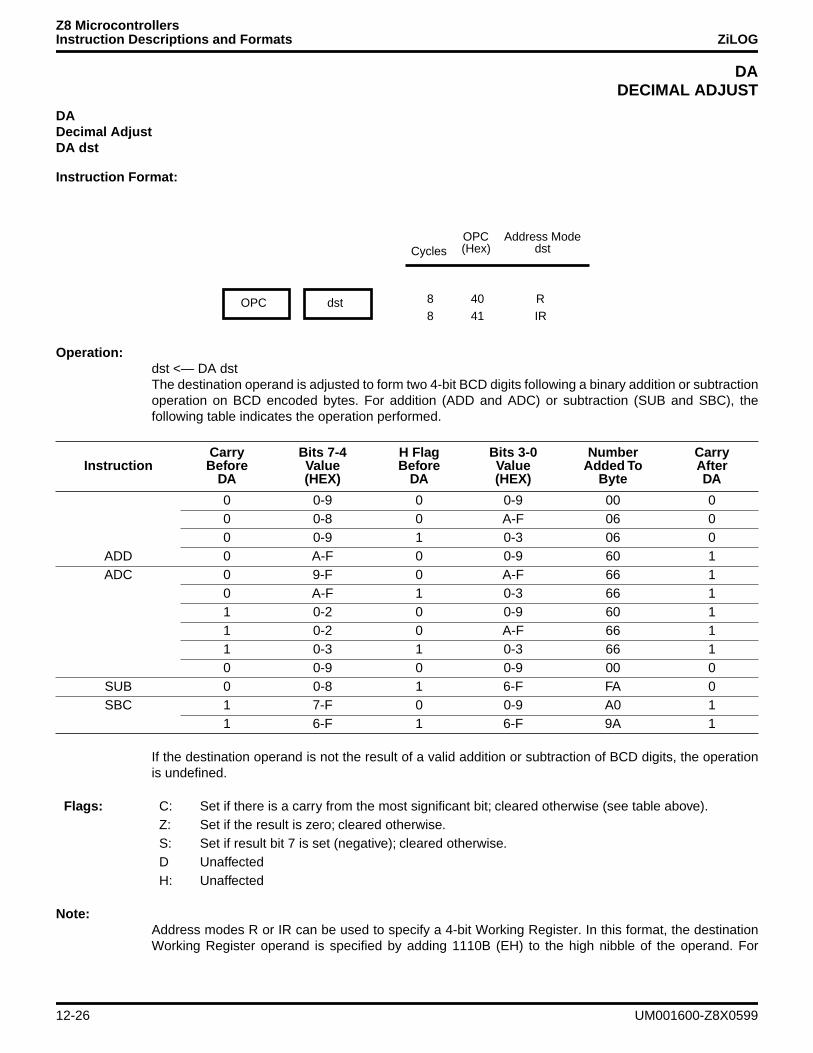
Z8 MicrocontrollersInstruction Descriptions and Formats ZiLOG
DADECIMAL ADJUST
DADecimal AdjustDA dst
Instruction Format:
Operation:dst <— DA dstThe destination operand is adjusted to form two 4-bit BCD digits following a binary addition or subtractionoperation on BCD encoded bytes. For addition (ADD and ADC) or subtraction (SUB and SBC), thefollowing table indicates the operation performed.
If the destination operand is not the result of a valid addition or subtraction of BCD digits, the operationis undefined.
Note:Address modes R or IR can be used to specify a 4-bit Working Register. In this format, the destinationWorking Register operand is specified by adding 1110B (EH) to the high nibble of the operand. For
Carry Bits 7-4 H Flag Bits 3-0 Number CarryInstruction Before Value Before Value Added To After
DA (HEX) DA (HEX) Byte DA
0 0-9 0 0-9 00 00 0-8 0 A-F 06 00 0-9 1 0-3 06 0
ADD 0 A-F 0 0-9 60 1ADC 0 9-F 0 A-F 66 1
0 A-F 1 0-3 66 11 0-2 0 0-9 60 11 0-2 0 A-F 66 11 0-3 1 0-3 66 10 0-9 0 0-9 00 0
SUB 0 0-8 1 6-F FA 0SBC 1 7-F 0 0-9 A0 1
1 6-F 1 6-F 9A 1
Flags: C: Set if there is a carry from the most significant bit; cleared otherwise (see table above).Z: Set if the result is zero; cleared otherwise.S: Set if result bit 7 is set (negative); cleared otherwise.D UnaffectedH: Unaffected
OPC dst 8
CyclesOPC(Hex)
Address Modedst
40 R8 41 IR
12-26 UM001600-Z8X0599
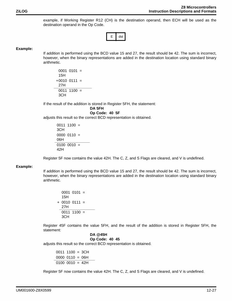
Z8 MicrocontrollersZiLOG Instruction Descriptions and Formats
example, if Working Register R12 (CH) is the destination operand, then ECH will be used as thedestination operand in the Op Code.
Example:If addition is performed using the BCD value 15 and 27, the result should be 42. The sum is incorrect,however, when the binary representations are added in the destination location using standard binaryarithmetic.
If the result of the addition is stored in Register 5FH, the statement:DA 5FHOp Code: 40 5F
adjusts this result so the correct BCD representation is obtained.
Register 5F now contains the value 42H. The C, Z, and S Flags are cleared, and V is undefined.
Example:If addition is performed using the BCD value 15 and 27, the result should be 42. The sum is incorrect,however, when the binary representations are added in the destination location using standard binaryarithmetic.
Register 45F contains the value 5FH, and the result of the addition is stored in Register 5FH, thestatement:
DA @45HOp Code: 40 45
adjusts this result so the correct BCD representation is obtained.
Register 5F now contains the value 42H. The C, Z, and S Flags are cleared, and V is undefined.
E dst
0001 0101 = 15H
+0010 0111 = 27H0011 1100 = 3CH
0011 1100 = 3CH0000 0110 = 06H0100 0010 = 42H
0001 0101 = 15H
+ 0010 0111 = 27H0011 1100 = 3CH
0011 1100 = 3CH0000 0110 = 06H0100 0010 = 42H
UM001600-Z8X0599 12-27
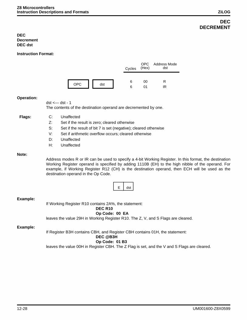
Z8 MicrocontrollersInstruction Descriptions and Formats ZiLOG
DECDECREMENT
DECDecrementDEC dst
Instruction Format:
Operation:dst <— dst - 1The contents of the destination operand are decremented by one.
Note:Address modes R or IR can be used to specify a 4-bit Working Register. In this format, the destinationWorking Register operand is specified by adding 1110B (EH) to the high nibble of the operand. Forexample, if Working Register R12 (CH) is the destination operand, then ECH will be used as thedestination operand in the Op Code.
Example:If Working Register R10 contains 2A%, the statement:
DEC R10Op Code: 00 EA
leaves the value 29H in Working Register R10. The Z, V, and S Flags are cleared.
Example:If Register B3H contains CBH, and Register CBH contains 01H, the statement:
DEC @B3HOp Code: 01 B3
leaves the value 00H in Register CBH. The Z Flag is set, and the V and S Flags are cleared.
OPC dst6
CyclesOPC(Hex)
Address Modedst
00 R6 01 IR
Flags: C: UnaffectedZ: Set if the result is zero; cleared otherwiseS: Set if the result of bit 7 is set (negative); cleared otherwiseV: Set if arithmetic overflow occurs; cleared otherwiseD: UnaffectedH: Unaffected
E dst
12-28 UM001600-Z8X0599
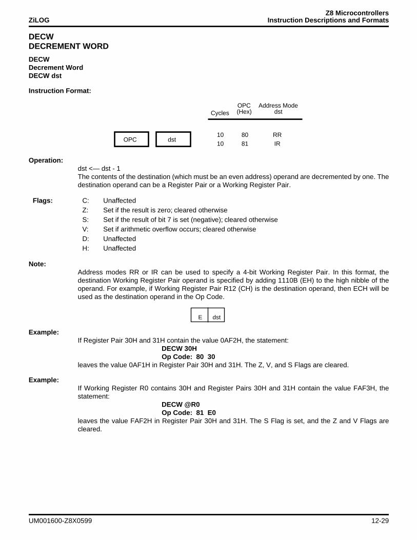
Z8 MicrocontrollersZiLOG Instruction Descriptions and Formats
DECWDECREMENT WORD
DECWDecrement WordDECW dst
Instruction Format:
Operation:dst <— dst - 1The contents of the destination (which must be an even address) operand are decremented by one. Thedestination operand can be a Register Pair or a Working Register Pair.
Note:Address modes RR or IR can be used to specify a 4-bit Working Register Pair. In this format, thedestination Working Register Pair operand is specified by adding 1110B (EH) to the high nibble of theoperand. For example, if Working Register Pair R12 (CH) is the destination operand, then ECH will beused as the destination operand in the Op Code.
Example:If Register Pair 30H and 31H contain the value 0AF2H, the statement:
DECW 30HOp Code: 80 30
leaves the value 0AF1H in Register Pair 30H and 31H. The Z, V, and S Flags are cleared.
Example:If Working Register R0 contains 30H and Register Pairs 30H and 31H contain the value FAF3H, thestatement:
DECW @R0Op Code: 81 E0
leaves the value FAF2H in Register Pair 30H and 31H. The S Flag is set, and the Z and V Flags arecleared.
OPC dst10
CyclesOPC(Hex)
Address Modedst
80 RR10 81 IR
Flags: C: UnaffectedZ: Set if the result is zero; cleared otherwiseS: Set if the result of bit 7 is set (negative); cleared otherwiseV: Set if arithmetic overflow occurs; cleared otherwiseD: UnaffectedH: Unaffected
E dst
UM001600-Z8X0599 12-29
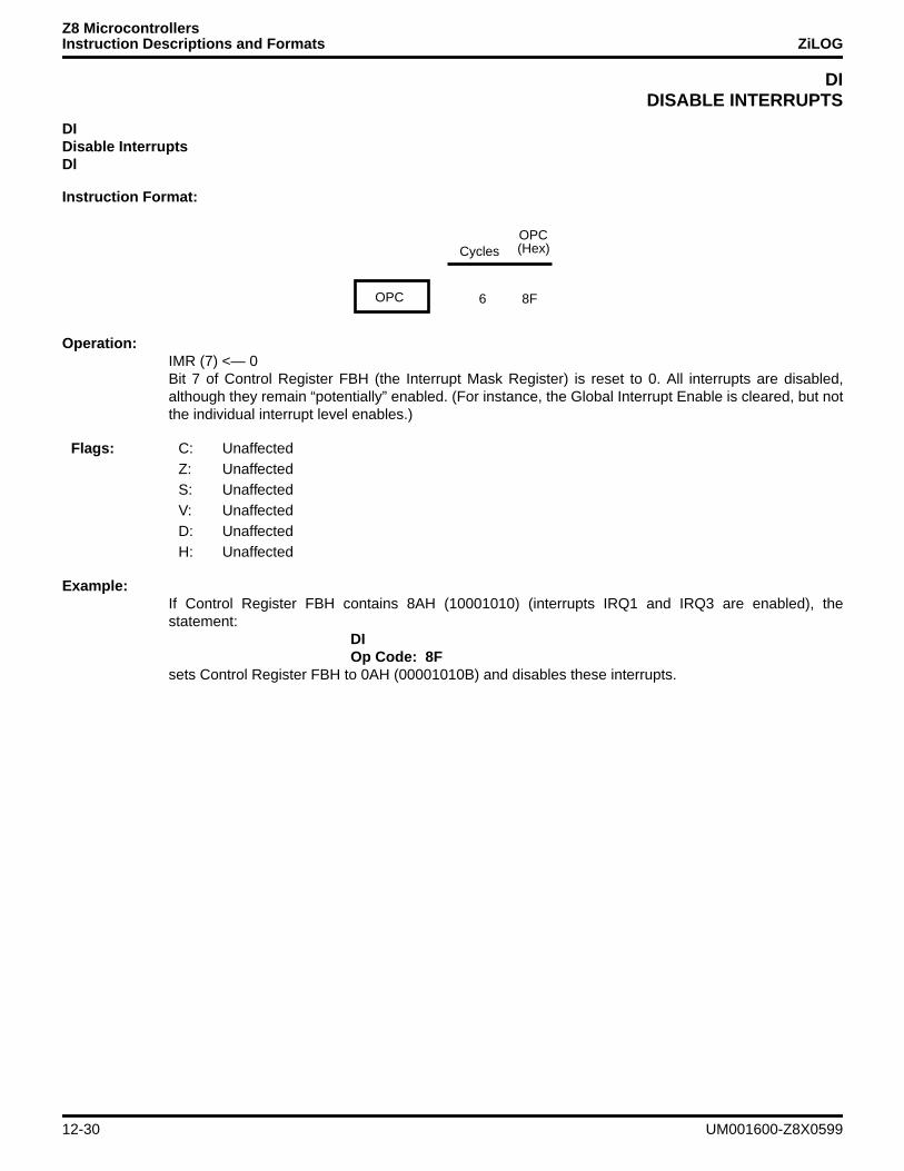
Z8 MicrocontrollersInstruction Descriptions and Formats ZiLOG
DIDISABLE INTERRUPTS
DIDisable InterruptsDl
Instruction Format:
Operation:IMR (7) <— 0Bit 7 of Control Register FBH (the Interrupt Mask Register) is reset to 0. All interrupts are disabled,although they remain “potentially” enabled. (For instance, the Global Interrupt Enable is cleared, but notthe individual interrupt level enables.)
Example:If Control Register FBH contains 8AH (10001010) (interrupts IRQ1 and IRQ3 are enabled), thestatement:
DIOp Code: 8F
sets Control Register FBH to 0AH (00001010B) and disables these interrupts.
OPC 6
CyclesOPC(Hex)
8F
Flags: C: UnaffectedZ: UnaffectedS: UnaffectedV: UnaffectedD: UnaffectedH: Unaffected
12-30 UM001600-Z8X0599
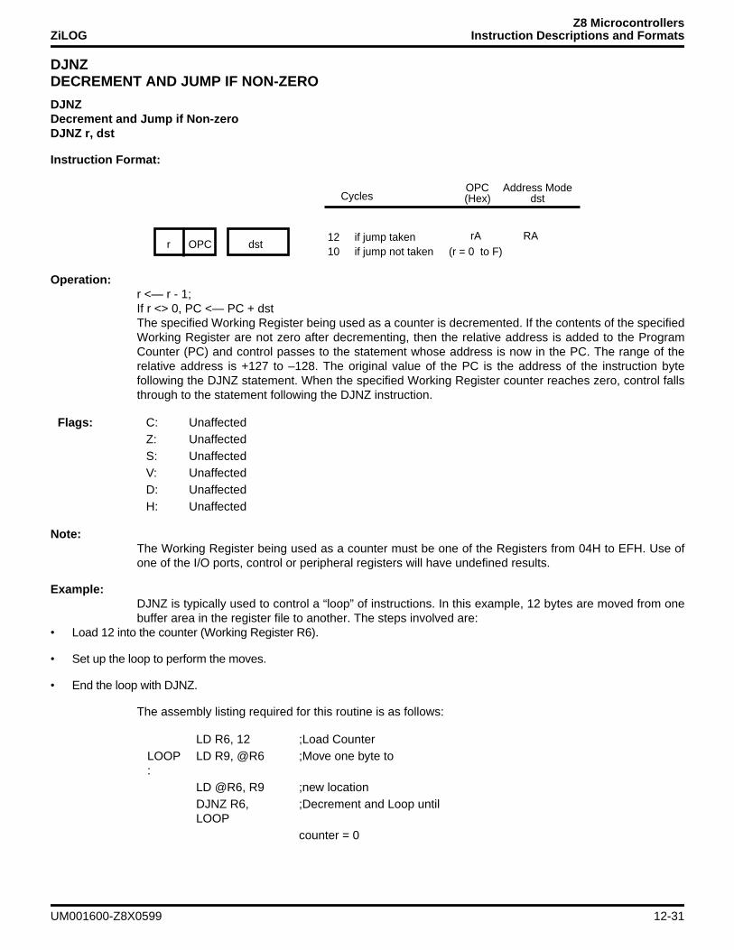
Z8 MicrocontrollersZiLOG Instruction Descriptions and Formats
DJNZDECREMENT AND JUMP IF NON-ZERO
DJNZDecrement and Jump if Non-zeroDJNZ r, dst
Instruction Format:
Operation:r <— r - 1;If r <> 0, PC <— PC + dstThe specified Working Register being used as a counter is decremented. If the contents of the specifiedWorking Register are not zero after decrementing, then the relative address is added to the ProgramCounter (PC) and control passes to the statement whose address is now in the PC. The range of therelative address is +127 to –128. The original value of the PC is the address of the instruction bytefollowing the DJNZ statement. When the specified Working Register counter reaches zero, control fallsthrough to the statement following the DJNZ instruction.
Note:The Working Register being used as a counter must be one of the Registers from 04H to EFH. Use ofone of the I/O ports, control or peripheral registers will have undefined results.
Example:DJNZ is typically used to control a “loop” of instructions. In this example, 12 bytes are moved from onebuffer area in the register file to another. The steps involved are:
• Load 12 into the counter (Working Register R6).
• Set up the loop to perform the moves.
• End the loop with DJNZ.
The assembly listing required for this routine is as follows:
r dst12 if jump taken
CyclesOPC(Hex)
Address Modedst
rA RA10 if jump not taken (r = 0 to F)
OPC
Flags: C: UnaffectedZ: UnaffectedS: UnaffectedV: UnaffectedD: UnaffectedH: Unaffected
LD R6, 12 ;Load Counter LOOP:
LD R9, @R6 ;Move one byte to
LD @R6, R9 ;new locationDJNZ R6, LOOP
;Decrement and Loop until
counter = 0
UM001600-Z8X0599 12-31

Z8 MicrocontrollersInstruction Descriptions and Formats ZiLOG
EIENABLE INTERRUPTS
EIEnable InterruptsEI
Instruction Format:
Operation:IMR (7) <— 0Bit 7 of Control Register FBH (the Interrupt Mask Register) is set to 1. This allows potentially enabledinterrupts to become enabled.
Example:If Control Register FBH contains 0AH (00001010) (interrupts IRQ1 and IRQ3 are selected), thestatement:
EIOp Code: 9F
sets Control Register FBH to 8AH (10001010B) and enables IRQ1 and IRQ3.
OPC 6
CyclesOPC(Hex)
9F
Flags: C: UnaffectedZ: UnaffectedS: UnaffectedV: UnaffectedD: UnaffectedH: Unaffected
12-32 UM001600-Z8X0599
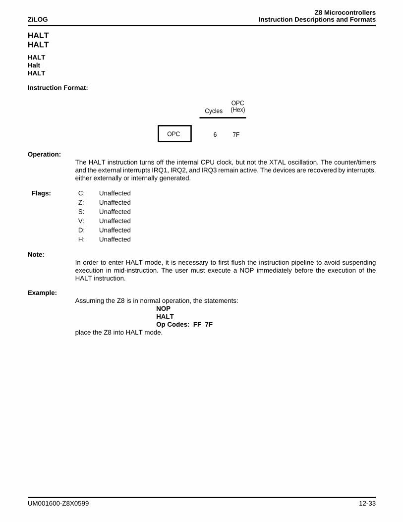
Z8 MicrocontrollersZiLOG Instruction Descriptions and Formats
HALTHALT
HALTHaltHALT
Instruction Format:
Operation:The HALT instruction turns off the internal CPU clock, but not the XTAL oscillation. The counter/timersand the external interrupts IRQ1, IRQ2, and IRQ3 remain active. The devices are recovered by interrupts,either externally or internally generated.
Note:In order to enter HALT mode, it is necessary to first flush the instruction pipeline to avoid suspendingexecution in mid-instruction. The user must execute a NOP immediately before the execution of theHALT instruction.
Example:Assuming the Z8 is in normal operation, the statements:
NOPHALTOp Codes: FF 7F
place the Z8 into HALT mode.
OPC 6
CyclesOPC(Hex)
7F
Flags: C: UnaffectedZ: UnaffectedS: UnaffectedV: UnaffectedD: UnaffectedH: Unaffected
UM001600-Z8X0599 12-33
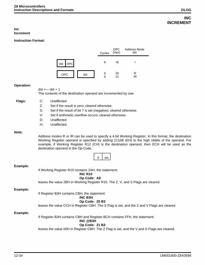
Z8 MicrocontrollersInstruction Descriptions and Formats ZiLOG
INCINCREMENT
IncIncrement
Instruction Format:
Operation:dst <— dst + 1The contents of the destination operand are incremented by one.
Note:Address modes R or IR can be used to specify a 4-bit Working Register. In this format, the destinationWorking Register operand is specified by adding 1110B (EH) to the high nibble of the operand. Forexample, if Working Register R12 (CH) is the destination operand, then ECH will be used as thedestination operand in the Op Code.
Example:If Working Register R10 contains 2AH, the statement:
INC R10Op Code: AE
leaves the value 2BH in Working Register R10. The Z, V, and S Flags are cleared.
Example:If Register B3H contains CBH, the statement:
INC B3HOp Code: 20 B3
leaves the value CCH in Register CBH. The S Flag is set, and the Z and V Flags are cleared.
Example:If Register B3H contains CBH and Register BCH contains FFH, the statement:
INC @B3HOp Code: 21 B3
leaves the value 00H in Register CBH. The Z Flag is set, and the V and S Flags are cleared.
dst OPC
OPC dst
6
CyclesOPC(Hex)
Address Modedst
rE r
6 20 R6 21 IR
Flags: C: UnaffectedZ: Set if the result is zero; cleared otherwise.S: Set if the result of bit 7 is set (negative); cleared otherwise.V: Set if arithmetic overflow occurs; cleared otherwise.D: UnaffectedH: Unaffected
E dst
12-34 UM001600-Z8X0599
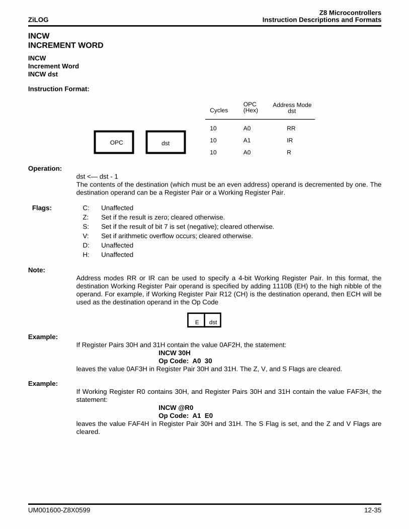
Z8 MicrocontrollersZiLOG Instruction Descriptions and Formats
INCWINCREMENT WORD
INCWIncrement WordINCW dst
Instruction Format:
Operation:dst <— dst - 1The contents of the destination (which must be an even address) operand is decremented by one. Thedestination operand can be a Register Pair or a Working Register Pair.
Note:Address modes RR or IR can be used to specify a 4-bit Working Register Pair. In this format, thedestination Working Register Pair operand is specified by adding 1110B (EH) to the high nibble of theoperand. For example, if Working Register Pair R12 (CH) is the destination operand, then ECH will beused as the destination operand in the Op Code
Example:If Register Pairs 30H and 31H contain the value 0AF2H, the statement:
INCW 30HOp Code: A0 30
leaves the value 0AF3H in Register Pair 30H and 31H. The Z, V, and S Flags are cleared.
Example:If Working Register R0 contains 30H, and Register Pairs 30H and 31H contain the value FAF3H, thestatement:
INCW @R0Op Code: A1 E0
leaves the value FAF4H in Register Pair 30H and 31H. The S Flag is set, and the Z and V Flags arecleared.
OPC dst
CyclesOPC Address Mode(Hex) dst
10
10
10
A0
A1
A0
RR
IR
R
Flags: C: UnaffectedZ: Set if the result is zero; cleared otherwise.S: Set if the result of bit 7 is set (negative); cleared otherwise.V: Set if arithmetic overflow occurs; cleared otherwise.D: UnaffectedH: Unaffected
E dst
UM001600-Z8X0599 12-35
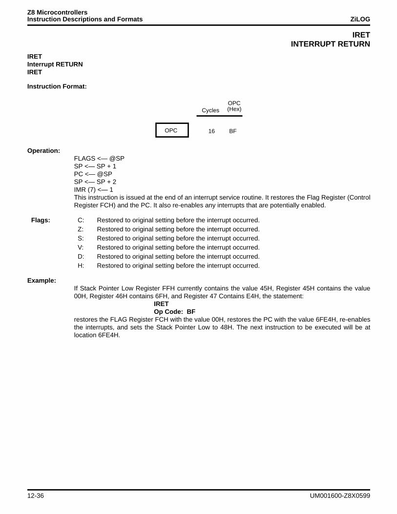
Z8 MicrocontrollersInstruction Descriptions and Formats ZiLOG
IRETINTERRUPT RETURN
IRETInterrupt RETURNIRET
Instruction Format:
Operation:FLAGS <— @SPSP <— SP + 1PC <— @SPSP <— SP + 2IMR (7) <— 1This instruction is issued at the end of an interrupt service routine. It restores the Flag Register (ControlRegister FCH) and the PC. It also re-enables any interrupts that are potentially enabled.
Example:If Stack Pointer Low Register FFH currently contains the value 45H, Register 45H contains the value00H, Register 46H contains 6FH, and Register 47 Contains E4H, the statement:
IRETOp Code: BF
restores the FLAG Register FCH with the value 00H, restores the PC with the value 6FE4H, re-enablesthe interrupts, and sets the Stack Pointer Low to 48H. The next instruction to be executed will be atlocation 6FE4H.
OPC 16
CyclesOPC(Hex)
BF
Flags: C: Restored to original setting before the interrupt occurred.Z: Restored to original setting before the interrupt occurred.S: Restored to original setting before the interrupt occurred.V: Restored to original setting before the interrupt occurred.D: Restored to original setting before the interrupt occurred.H: Restored to original setting before the interrupt occurred.
12-36 UM001600-Z8X0599
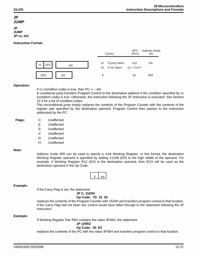
Z8 MicrocontrollersZiLOG Instruction Descriptions and Formats
JPJUMP
JPJUMPJP cc, dst
Instruction Format:
Operation:If cc (condition code) is true, then PC <— dstA conditional jump transfers Program Control to the destination address if the condition specified by cc(condition code) is true. Otherwise, the instruction following the JP instruction is executed. See Section12.3 for a list of condition codes.The unconditional jump simply replaces the contents of the Program Counter with the contents of theregister pair specified by the destination operand. Program Control then passes to the instructionaddressed by the PC.
Note:Address mode IRR can be used to specify a 4-bit Working Register. In this format, the destinationWorking Register operand is specified by adding 1110B (EH) to the high nibble of the operand. Forexample, if Working Register R12 (CH) is the destination operand, then ECH will be used as thedestination operand in the Op Code.
Example:If the Carry Flag is set, the statement:
JP C, 1520HOp Code: 7D 15 20
replaces the contents of the Program Counter with 1520H and transfers program control to that location.If the Carry Flag had not been set, control would have fallen through to the statement following the JPinstruction.
Example:If Working Register Pair RR2 contains the value 3F45H, the statement:
JP @RR2Op Code: 30 E2
replaces the contents of the PC with the value 3F45H and transfers program control to that location.
dstOPC
OPC dst
Cycles
12 if jump taken
8
10 if not taken
OPC(Hex)
Address Modedst
ccD DA
30 IRR
cc = 0 to Fcc
Flags: C: UnaffectedZ: UnaffectedS: UnaffectedV: UnaffectedD: UnaffectedH: Unaffected
E dst
UM001600-Z8X0599 12-37
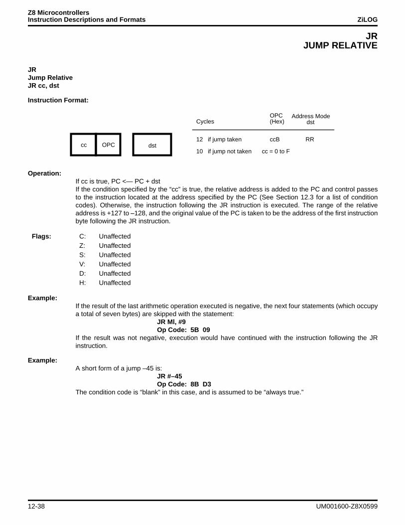
Z8 MicrocontrollersInstruction Descriptions and Formats ZiLOG
JRJUMP RELATIVE
JRJump RelativeJR cc, dst
Instruction Format:
Operation:If cc is true, PC <— PC + dstIf the condition specified by the “cc” is true, the relative address is added to the PC and control passesto the instruction located at the address specified by the PC (See Section 12.3 for a list of conditioncodes). Otherwise, the instruction following the JR instruction is executed. The range of the relativeaddress is +127 to –128, and the original value of the PC is taken to be the address of the first instructionbyte following the JR instruction.
Example:If the result of the last arithmetic operation executed is negative, the next four statements (which occupya total of seven bytes) are skipped with the statement:
JR Ml, #9Op Code: 5B 09
If the result was not negative, execution would have continued with the instruction following the JRinstruction.
Example:A short form of a jump –45 is:
JR #–45Op Code: 8B D3
The condition code is “blank” in this case, and is assumed to be “always true.”
dst
CyclesOPC Address Mode(Hex) dst
12 if jump taken
10 if jump not taken
ccB
cc = 0 to F
RR cc OPC
Flags: C: UnaffectedZ: UnaffectedS: UnaffectedV: UnaffectedD: UnaffectedH: Unaffected
12-38 UM001600-Z8X0599
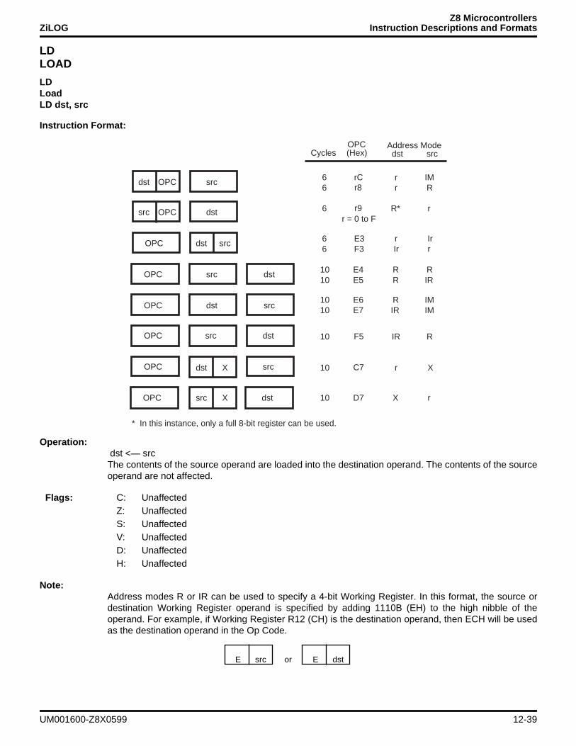
Z8 MicrocontrollersZiLOG Instruction Descriptions and Formats
LDLOAD
LDLoadLD dst, src
Instruction Format:
Operation: dst <— srcThe contents of the source operand are loaded into the destination operand. The contents of the sourceoperand are not affected.
Note:Address modes R or IR can be used to specify a 4-bit Working Register. In this format, the source ordestination Working Register operand is specified by adding 1110B (EH) to the high nibble of theoperand. For example, if Working Register R12 (CH) is the destination operand, then ECH will be usedas the destination operand in the Op Code.
dst OPC src 6
CyclesOPC(Hex)
Address Mode dst src
rC r IM6 r8 r R
OPC
dst 6 r9 R* rr = 0 to F
6 E3 r Ir6 F3 Ir r
OPC
OPC
src
dst
dst
src
10 E4 R R10 E5 R IR
10 E6 R IM10 E7 IR IM
OPC
OPC
src dst
src
OPC dst
src OPC
dst src
dst X
src X
10 F5 IR R
10 r X
10 D7 X r
* In this instance, only a full 8-bit register can be used.
C7
Flags: C: UnaffectedZ: UnaffectedS: UnaffectedV: UnaffectedD: UnaffectedH: Unaffected
E src E dstor
UM001600-Z8X0599 12-39
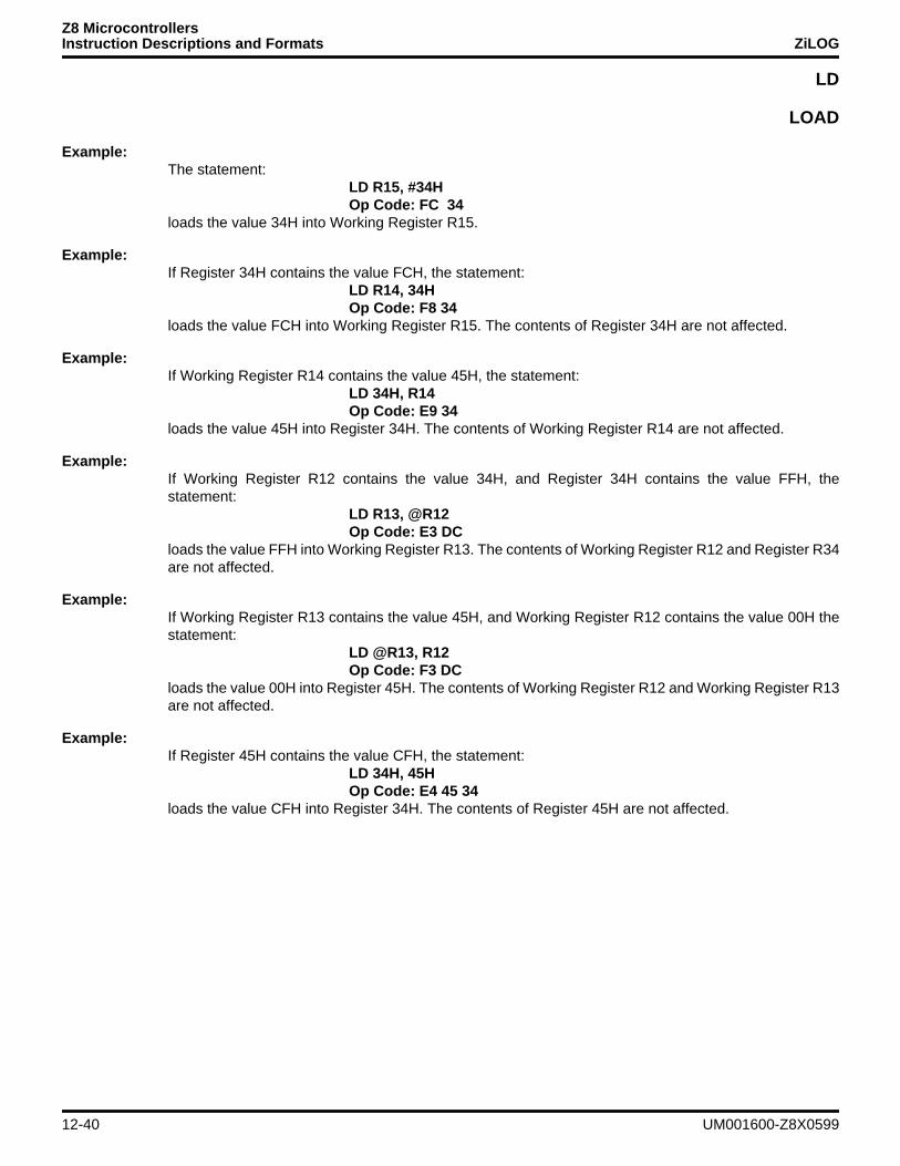
Z8 MicrocontrollersInstruction Descriptions and Formats ZiLOG
LD
LOAD
Example:The statement:
LD R15, #34HOp Code: FC 34
loads the value 34H into Working Register R15.
Example:If Register 34H contains the value FCH, the statement:
LD R14, 34HOp Code: F8 34
loads the value FCH into Working Register R15. The contents of Register 34H are not affected.
Example:If Working Register R14 contains the value 45H, the statement:
LD 34H, R14Op Code: E9 34
loads the value 45H into Register 34H. The contents of Working Register R14 are not affected.
Example:If Working Register R12 contains the value 34H, and Register 34H contains the value FFH, thestatement:
LD R13, @R12Op Code: E3 DC
loads the value FFH into Working Register R13. The contents of Working Register R12 and Register R34are not affected.
Example:If Working Register R13 contains the value 45H, and Working Register R12 contains the value 00H thestatement:
LD @R13, R12Op Code: F3 DC
loads the value 00H into Register 45H. The contents of Working Register R12 and Working Register R13are not affected.
Example:If Register 45H contains the value CFH, the statement:
LD 34H, 45HOp Code: E4 45 34
loads the value CFH into Register 34H. The contents of Register 45H are not affected.
12-40 UM001600-Z8X0599
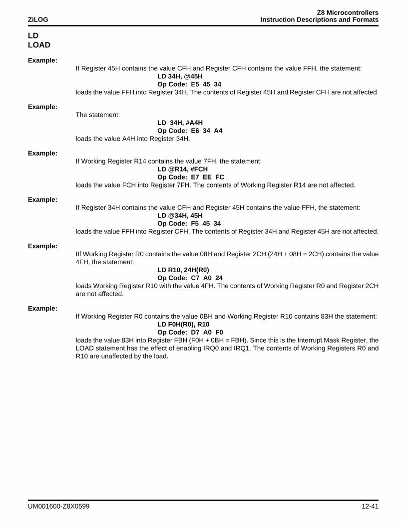
Z8 MicrocontrollersZiLOG Instruction Descriptions and Formats
LDLOAD
Example:If Register 45H contains the value CFH and Register CFH contains the value FFH, the statement:
LD 34H, @45HOp Code: E5 45 34
loads the value FFH into Register 34H. The contents of Register 45H and Register CFH are not affected.
Example:The statement:
LD 34H, #A4HOp Code: E6 34 A4
loads the value A4H into Register 34H.
Example:If Working Register R14 contains the value 7FH, the statement:
LD @R14, #FCHOp Code: E7 EE FC
loads the value FCH into Register 7FH. The contents of Working Register R14 are not affected.
Example:If Register 34H contains the value CFH and Register 45H contains the value FFH, the statement:
LD @34H, 45HOp Code: F5 45 34
loads the value FFH into Register CFH. The contents of Register 34H and Register 45H are not affected.
Example:IIf Working Register R0 contains the value 08H and Register 2CH (24H + 08H = 2CH) contains the value4FH, the statement:
LD R10, 24H(R0)Op Code: C7 A0 24
loads Working Register R10 with the value 4FH. The contents of Working Register R0 and Register 2CHare not affected.
Example:If Working Register R0 contains the value 0BH and Working Register R10 contains 83H the statement:
LD F0H(R0), R10Op Code: D7 A0 F0
loads the value 83H into Register FBH (F0H + 0BH = FBH). Since this is the Interrupt Mask Register, theLOAD statement has the effect of enabling IRQ0 and IRQ1. The contents of Working Registers R0 andR10 are unaffected by the load.
UM001600-Z8X0599 12-41
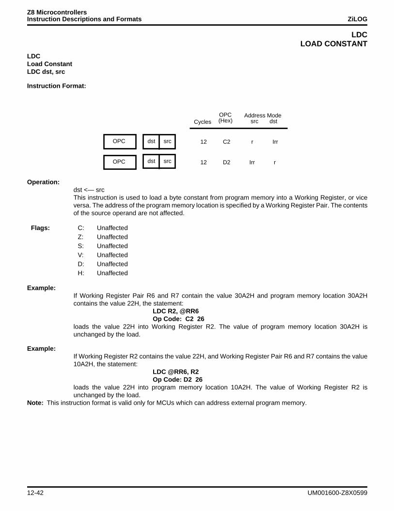
Z8 MicrocontrollersInstruction Descriptions and Formats ZiLOG
LDCLOAD CONSTANT
LDCLoad ConstantLDC dst, src
Instruction Format:
Operation:dst <— srcThis instruction is used to load a byte constant from program memory into a Working Register, or viceversa. The address of the program memory location is specified by a Working Register Pair. The contentsof the source operand are not affected.
Example:If Working Register Pair R6 and R7 contain the value 30A2H and program memory location 30A2Hcontains the value 22H, the statement:
LDC R2, @RR6Op Code: C2 26
loads the value 22H into Working Register R2. The value of program memory location 30A2H isunchanged by the load.
Example:If Working Register R2 contains the value 22H, and Working Register Pair R6 and R7 contains the value10A2H, the statement:
LDC @RR6, R2Op Code: D2 26
loads the value 22H into program memory location 10A2H. The value of Working Register R2 isunchanged by the load.
Note: This instruction format is valid only for MCUs which can address external program memory.
12
CyclesOPC(Hex)
Address Mode src dst
C2 r Irr
12 D2 Irr r
dst srcOPC
OPC dst src
Flags: C: UnaffectedZ: UnaffectedS: UnaffectedV: UnaffectedD: UnaffectedH: Unaffected
12-42 UM001600-Z8X0599
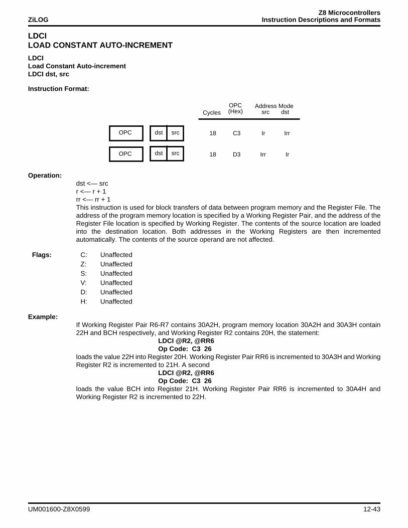
Z8 MicrocontrollersZiLOG Instruction Descriptions and Formats
LDCILOAD CONSTANT AUTO-INCREMENT
LDCILoad Constant Auto-incrementLDCI dst, src
Instruction Format:
Operation:dst <— srcr <— r + 1rr <— rr + 1This instruction is used for block transfers of data between program memory and the Register File. Theaddress of the program memory location is specified by a Working Register Pair, and the address of theRegister File location is specified by Working Register. The contents of the source location are loadedinto the destination location. Both addresses in the Working Registers are then incrementedautomatically. The contents of the source operand are not affected.
Example:If Working Register Pair R6-R7 contains 30A2H, program memory location 30A2H and 30A3H contain22H and BCH respectively, and Working Register R2 contains 20H, the statement:
LDCI @R2, @RR6Op Code: C3 26
loads the value 22H into Register 20H. Working Register Pair RR6 is incremented to 30A3H and WorkingRegister R2 is incremented to 21H. A second
LDCI @R2, @RR6Op Code: C3 26
loads the value BCH into Register 21H. Working Register Pair RR6 is incremented to 30A4H andWorking Register R2 is incremented to 22H.
18
CyclesOPC(Hex)
Address Mode src dst
C3 Ir Irr
18 D3 Irr Ir
dst srcOPC
OPC dst src
Flags: C: UnaffectedZ: UnaffectedS: UnaffectedV: UnaffectedD: UnaffectedH: Unaffected
UM001600-Z8X0599 12-43

Z8 MicrocontrollersInstruction Descriptions and Formats ZiLOG
LDCILOAD CONSTANT AUTO-INCREMENT
Example:If Working Register R2 contains 20H, Register 20H contains 22H, Register 21H contains BCH, andWorking Register Pair R6-R7 contains 30A2H, the statement:
LDCI @RR6, @R2Op Code: D3 26
loads the value 22H into program memory location 30A2H. Working Register R2 is incremented to 21Hand Working Register Pair R6-R7 is incremented to 30A3H. A second
LDCI @RR6, @R2Op Code: D3 26
loads the value BCH into program memory location 30A3H. Working Register R2 is incremented to 22Hand Working Register Pair R6-R7 is incremented to 30A4H.
12-44 UM001600-Z8X0599
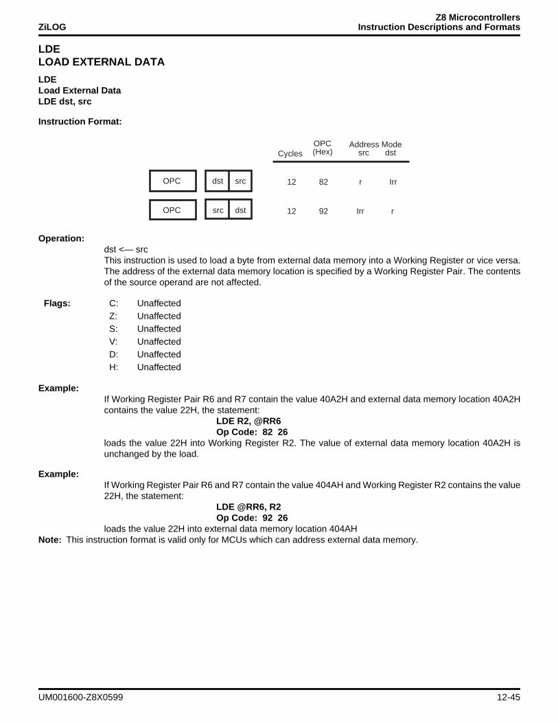
Z8 MicrocontrollersZiLOG Instruction Descriptions and Formats
LDELOAD EXTERNAL DATA
LDELoad External DataLDE dst, src
Instruction Format:
Operation:dst <— srcThis instruction is used to load a byte from external data memory into a Working Register or vice versa.The address of the external data memory location is specified by a Working Register Pair. The contentsof the source operand are not affected.
Example:If Working Register Pair R6 and R7 contain the value 40A2H and external data memory location 40A2Hcontains the value 22H, the statement:
LDE R2, @RR6Op Code: 82 26
loads the value 22H into Working Register R2. The value of external data memory location 40A2H isunchanged by the load.
Example:If Working Register Pair R6 and R7 contain the value 404AH and Working Register R2 contains the value22H, the statement:
LDE @RR6, R2Op Code: 92 26
loads the value 22H into external data memory location 404AHNote: This instruction format is valid only for MCUs which can address external data memory.
12
CyclesOPC(Hex)
Address Mode src dst
82 r Irr
12 92 Irr r
dst srcOPC
OPC dstsrc
Flags: C: UnaffectedZ: UnaffectedS: UnaffectedV: UnaffectedD: UnaffectedH: Unaffected
UM001600-Z8X0599 12-45
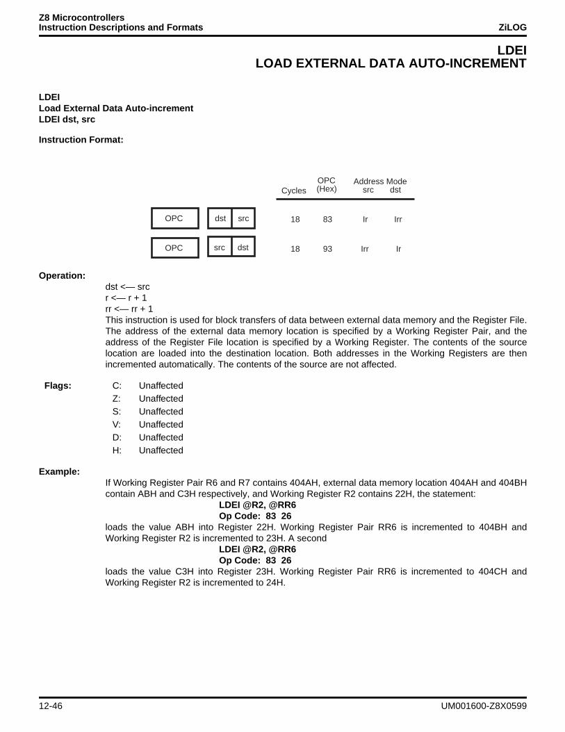
Z8 MicrocontrollersInstruction Descriptions and Formats ZiLOG
LDEILOAD EXTERNAL DATA AUTO-INCREMENT
LDEILoad External Data Auto-incrementLDEI dst, src
Instruction Format:
Operation:dst <— srcr <— r + 1rr <— rr + 1This instruction is used for block transfers of data between external data memory and the Register File.The address of the external data memory location is specified by a Working Register Pair, and theaddress of the Register File location is specified by a Working Register. The contents of the sourcelocation are loaded into the destination location. Both addresses in the Working Registers are thenincremented automatically. The contents of the source are not affected.
Example:If Working Register Pair R6 and R7 contains 404AH, external data memory location 404AH and 404BHcontain ABH and C3H respectively, and Working Register R2 contains 22H, the statement:
LDEI @R2, @RR6Op Code: 83 26
loads the value ABH into Register 22H. Working Register Pair RR6 is incremented to 404BH andWorking Register R2 is incremented to 23H. A second
LDEI @R2, @RR6Op Code: 83 26
loads the value C3H into Register 23H. Working Register Pair RR6 is incremented to 404CH andWorking Register R2 is incremented to 24H.
18
CyclesOPC(Hex)
Address Mode src dst
83 Ir Irr
18 93 Irr Ir
dst srcOPC
OPC dstsrc
Flags: C: UnaffectedZ: UnaffectedS: UnaffectedV: UnaffectedD: UnaffectedH: Unaffected
12-46 UM001600-Z8X0599
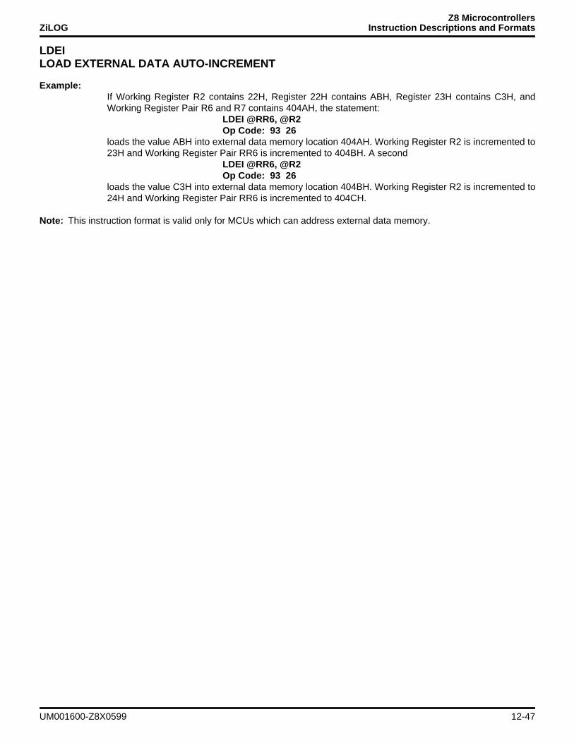
Z8 MicrocontrollersZiLOG Instruction Descriptions and Formats
LDEILOAD EXTERNAL DATA AUTO-INCREMENT
Example:If Working Register R2 contains 22H, Register 22H contains ABH, Register 23H contains C3H, andWorking Register Pair R6 and R7 contains 404AH, the statement:
LDEI @RR6, @R2Op Code: 93 26
loads the value ABH into external data memory location 404AH. Working Register R2 is incremented to23H and Working Register Pair RR6 is incremented to 404BH. A second
LDEI @RR6, @R2Op Code: 93 26
loads the value C3H into external data memory location 404BH. Working Register R2 is incremented to24H and Working Register Pair RR6 is incremented to 404CH.
Note: This instruction format is valid only for MCUs which can address external data memory.
UM001600-Z8X0599 12-47
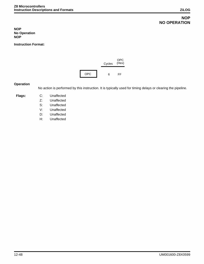
Z8 MicrocontrollersInstruction Descriptions and Formats ZiLOG
NOPNO OPERATION
NOPNo OperationNOP
Instruction Format:
OperationNo action is performed by this instruction. It is typically used for timing delays or clearing the pipeline.
OPC 6
CyclesOPC(Hex)
FF
Flags: C: UnaffectedZ: UnaffectedS: UnaffectedV: UnaffectedD: UnaffectedH: Unaffected
12-48 UM001600-Z8X0599
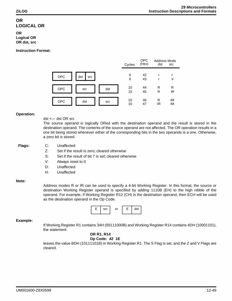
Z8 MicrocontrollersZiLOG Instruction Descriptions and Formats
ORLOGICAL OR
ORLogical OROR dst, src
Instruction Format:
Operation:dst <— dst OR srcThe source operand is logically ORed with the destination operand and the result is stored in thedestination operand. The contents of the source operand are not affected. The OR operation results in aone bit being stored whenever either of the corresponding bits in the two operands is a one. Otherwise,a zero bit is stored.
Note:Address modes R or IR can be used to specify a 4-bit Working Register. In this format, the source ordestination Working Register operand is specified by adding 1110B (EH) to the high nibble of theoperand. For example, if Working Register R12 (CH) is the destination operand, then ECH will be usedas the destination operand in the Op Code.
Example:If Working Register R1 contains 34H (00111000B) and Working Register R14 contains 4DH (10001101),the statement:
OR R1, R14Op Code: 42 1E
leaves the value BDH (10111101B) in Working Register R1. The S Flag is set, and the Z and V Flags arecleared.
dst srcOPC
OPC
OPC
src
dst
dst
src
6
CyclesOPC(Hex)
Address Mode dst src
42 r r6 43 r Ir
10 44 R R10 45 R IR
10 46 R IM10 47 IR IM
Flags: C: UnaffectedZ: Set if the result is zero; cleared otherwiseS: Set if the result of bit 7 is set; cleared otherwiseV: Always reset to 0D: UnaffectedH: Unaffected
E src E dstor
UM001600-Z8X0599 12-49
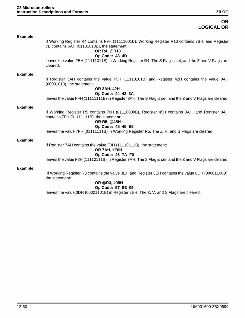
Z8 MicrocontrollersInstruction Descriptions and Formats ZiLOG
ORLOGICAL OR
Example:If Working Register R4 contains F9H (11111001B), Working Register R13 contains 7BH, and Register7B contains 6AH (01101010B), the statement:
OR R4, @R13Op Code: 43 4D
leaves the value FBH (11111011B) in Working Register R4. The S Flag is set, and the Z and V Flags arecleared.
Example:If Register 3AH contains the value F5H (11110101B) and Register 42H contains the value 0AH(00001010), the statement:
OR 3AH, 42HOp Code: 44 42 3A
leaves the value FFH (11111111B) in Register 3AH. The S Flag is set, and the Z and V Flags are cleared.
Example:If Working Register R5 contains 70H (01110000B), Register 45H contains 3AH, and Register 3AHcontains 7FH (01111111B), the statement:
OR R5, @45HOp Code: 45 45 E5
leaves the value 7FH (01111111B) in Working Register R5. The Z, V, and S Flags are cleared.
Example:If Register 7AH contains the value F3H (11110111B), the statement:
OR 7AH, #F0HOp Code: 46 7A F0
leaves the value F3H (11110111B) in Register 7AH. The S Flag is set, and the Z and V Flags are cleared.
Example: If Working Register R3 contains the value 3EH and Register 3EH contains the value 0CH (00001100B),the statement:
OR @R3, #05HOp Code: 57 E3 05
leaves the value 0DH (00001101B) in Register 3EH. The Z, V, and S Flags are cleared.
12-50 UM001600-Z8X0599

Z8 MicrocontrollersZiLOG Instruction Descriptions and Formats
POPPOP
POPPopPOP dst
Instruction Format:
Operation:dst <— @SPSP <— SP + 1The contents of the location specified by the SP (Stack Pointer) are loaded into the destination operand.The SP is then incremented automatically.
Note:Address modes R or IR can be used to specify a 4-bit Working Register. In this format, the destinationWorking Register operand is specified by adding 1110B (EH) to the high nibble of the operand. Forexample, if Working Register R12 (CH) is the destination operand, then ECH will be used as thedestination operand in the Op Code.
Example:If the SP (Control Registers FEH and FFH) contains the value 70H and Register 70H contains 44H, thestatement:
POP 34HOp Code: 50 34
loads the value 44H into Register 34H. After the POP operation, the SP contains 71H. The contents ofRegister 70 are not affected.
Example: If the SP (Control Registers FEH and FFH) contains the value 1000H, external data memory location1000H contains 55H, and Working Register R6 contains 22H, the statement:
POP @R6Op Code: 51 E6
loads the value 55H into Register 22H. After the POP operation, the SP contains 1001H. The contentsof Working Register R6 are not affected.
OPC dst 10
CyclesOPC(Hex)
Address Modedst
50 R10 51 IR
Flags: C: UnaffectedZ: UnaffectedS: UnaffectedV: UnaffectedD: UnaffectedH: Unaffected
E dst
UM001600-Z8X0599 12-51
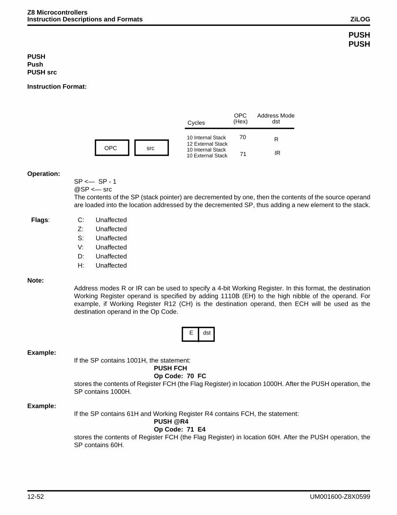
Z8 MicrocontrollersInstruction Descriptions and Formats ZiLOG
PUSHPUSH
PUSHPushPUSH src
Instruction Format:
Operation:SP <— SP - 1@SP <— srcThe contents of the SP (stack pointer) are decremented by one, then the contents of the source operandare loaded into the location addressed by the decremented SP, thus adding a new element to the stack.
Note:Address modes R or IR can be used to specify a 4-bit Working Register. In this format, the destinationWorking Register operand is specified by adding 1110B (EH) to the high nibble of the operand. Forexample, if Working Register R12 (CH) is the destination operand, then ECH will be used as thedestination operand in the Op Code.
Example:If the SP contains 1001H, the statement:
PUSH FCHOp Code: 70 FC
stores the contents of Register FCH (the Flag Register) in location 1000H. After the PUSH operation, theSP contains 1000H.
Example:If the SP contains 61H and Working Register R4 contains FCH, the statement:
PUSH @R4Op Code: 71 E4
stores the contents of Register FCH (the Flag Register) in location 60H. After the PUSH operation, theSP contains 60H.
OPC src
CyclesOPC(Hex)
Address Modedst
R
IR
10 Internal Stack12 External Stack10 Internal Stack10 External Stack
70
71
Flags : C: UnaffectedZ: UnaffectedS: UnaffectedV: UnaffectedD: UnaffectedH: Unaffected
E dst
12-52 UM001600-Z8X0599

Z8 MicrocontrollersZiLOG Instruction Descriptions and Formats
RCFRESET CARRY FLAG
RCFReset Carry FlagRCF
Instruction Format:
Operation:C <— 0The C Flag is reset to 0, regardless of its previous value.
Example: If the C Flag is currently set, the statement:
RCFOp Code: CF
resets the Carry Flag to 0.
OPC 6
CyclesOPC(Hex)
CF
Flags: C: Reset to 0Z: UnaffectedS: UnaffectedV: UnaffectedD: UnaffectedH: Unaffected
UM001600-Z8X0599 12-53
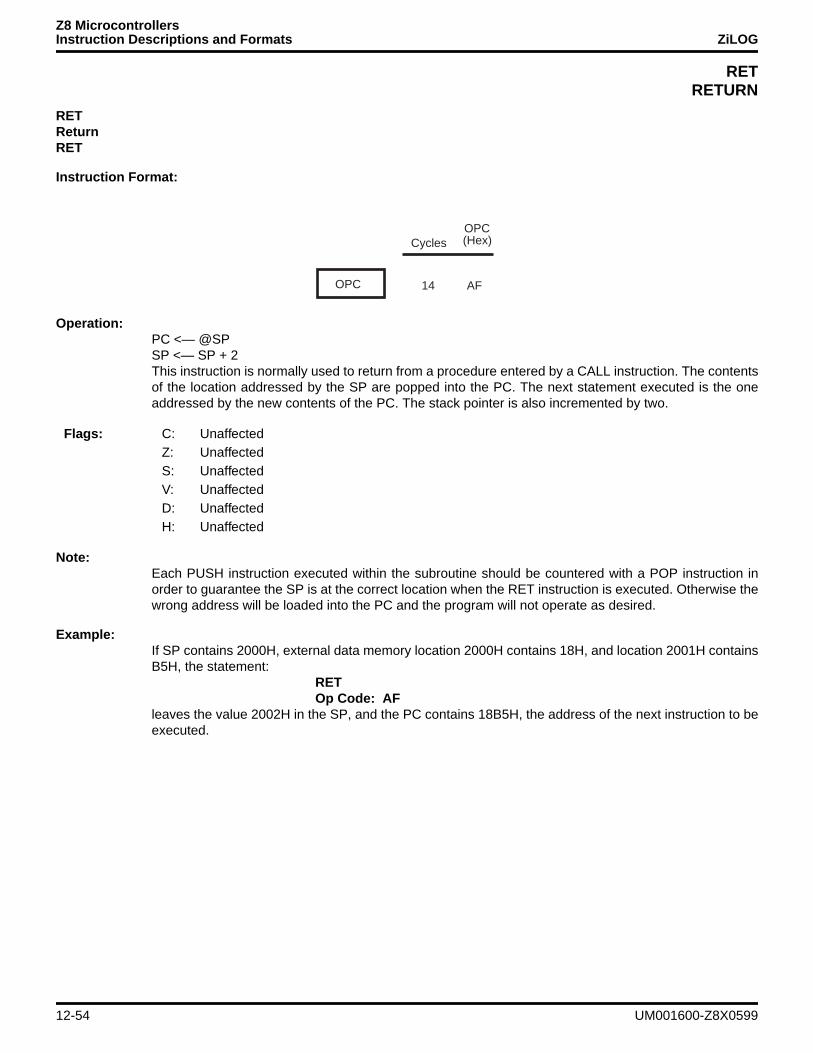
Z8 MicrocontrollersInstruction Descriptions and Formats ZiLOG
RETRETURN
RETReturnRET
Instruction Format:
Operation:PC <— @SPSP <— SP + 2This instruction is normally used to return from a procedure entered by a CALL instruction. The contentsof the location addressed by the SP are popped into the PC. The next statement executed is the oneaddressed by the new contents of the PC. The stack pointer is also incremented by two.
Note:Each PUSH instruction executed within the subroutine should be countered with a POP instruction inorder to guarantee the SP is at the correct location when the RET instruction is executed. Otherwise thewrong address will be loaded into the PC and the program will not operate as desired.
Example:If SP contains 2000H, external data memory location 2000H contains 18H, and location 2001H containsB5H, the statement:
RETOp Code: AF
leaves the value 2002H in the SP, and the PC contains 18B5H, the address of the next instruction to beexecuted.
OPC 14
CyclesOPC(Hex)
AF
Flags: C: UnaffectedZ: UnaffectedS: UnaffectedV: UnaffectedD: UnaffectedH: Unaffected
12-54 UM001600-Z8X0599
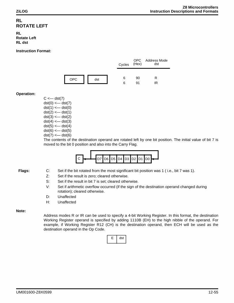
Z8 MicrocontrollersZiLOG Instruction Descriptions and Formats
RLROTATE LEFT
RLRotate LeftRL dst
Instruction Format:
Operation:C <— dst(7)dst(0) <— dst(7)dst(1) <— dst(0)dst(2) <— dst(1)dst(3) <— dst(2)dst(4) <— dst(3)dst(5) <— dst(4)dst(6) <— dst(5)dst(7) <— dst(6)The contents of the destination operand are rotated left by one bit position. The initial value of bit 7 ismoved to the bit 0 position and also into the Carry Flag.
Note:Address modes R or IR can be used to specify a 4-bit Working Register. In this format, the destinationWorking Register operand is specified by adding 1110B (EH) to the high nibble of the operand. Forexample, if Working Register R12 (CH) is the destination operand, then ECH will be used as thedestination operand in the Op Code.
OPC dst 6
CyclesOPC(Hex)
Address Modedst
90 R6 91 IR
D7 D6 D5 D4 D3 D2 D1 D0C
Flags: C: Set if the bit rotated from the most significant bit position was 1 ( i.e., bit 7 was 1).Z: Set if the result is zero; cleared otherwise.S: Set if the result in bit 7 is set; cleared otherwise.V: Set if arithmetic overflow occurred (if the sign of the destination operand changed during
rotation); cleared otherwise.D: UnaffectedH: Unaffected
E dst
UM001600-Z8X0599 12-55
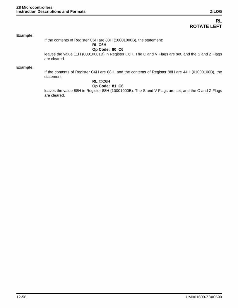
Z8 MicrocontrollersInstruction Descriptions and Formats ZiLOG
RLROTATE LEFT
Example:If the contents of Register C6H are 88H (10001000B), the statement:
RL C6HOp Code: 80 C6
leaves the value 11H (00010001B) in Register C6H. The C and V Flags are set, and the S and Z Flagsare cleared.
Example:If the contents of Register C6H are 88H, and the contents of Register 88H are 44H (01000100B), thestatement:
RL @C6HOp Code: 81 C6
leaves the value 88H in Register 88H (10001000B). The S and V Flags are set, and the C and Z Flagsare cleared.
12-56 UM001600-Z8X0599
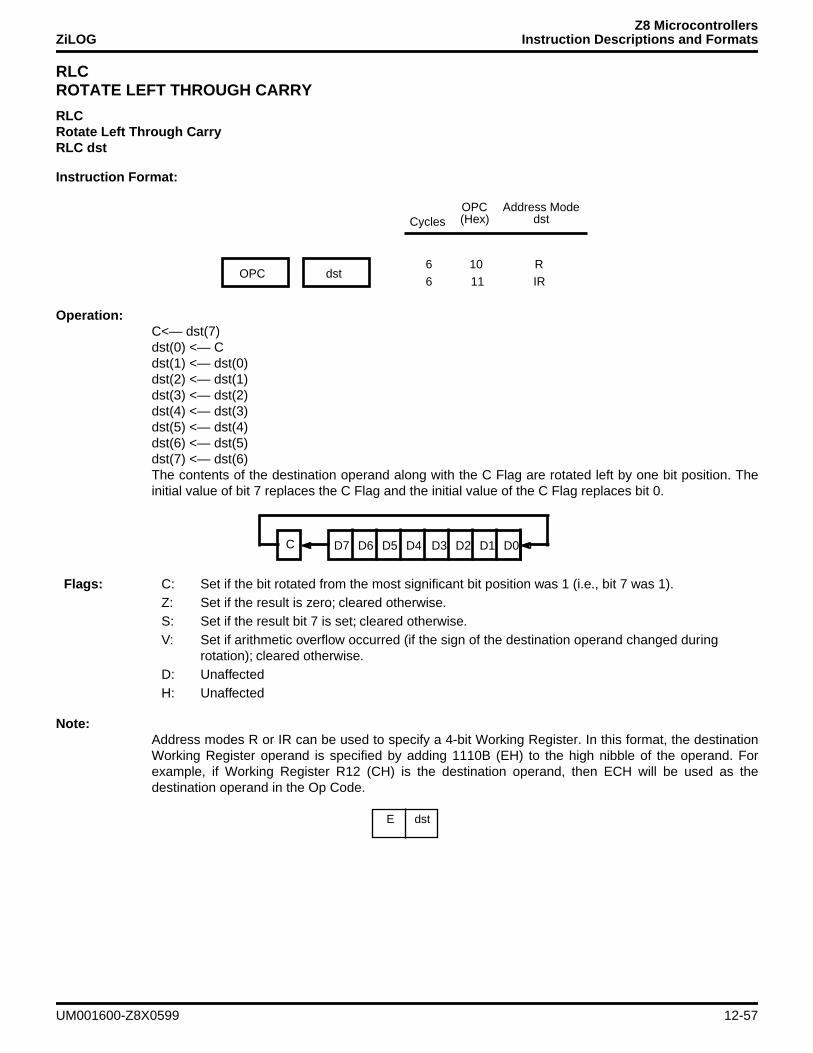
Z8 MicrocontrollersZiLOG Instruction Descriptions and Formats
RLCROTATE LEFT THROUGH CARRY
RLCRotate Left Through CarryRLC dst
Instruction Format:
Operation:C<— dst(7)dst(0) <— Cdst(1) <— dst(0)dst(2) <— dst(1)dst(3) <— dst(2)dst(4) <— dst(3)dst(5) <— dst(4)dst(6) <— dst(5)dst(7) <— dst(6)The contents of the destination operand along with the C Flag are rotated left by one bit position. Theinitial value of bit 7 replaces the C Flag and the initial value of the C Flag replaces bit 0.
Note:Address modes R or IR can be used to specify a 4-bit Working Register. In this format, the destinationWorking Register operand is specified by adding 1110B (EH) to the high nibble of the operand. Forexample, if Working Register R12 (CH) is the destination operand, then ECH will be used as thedestination operand in the Op Code.
OPC dst6
CyclesOPC(Hex)
Address Modedst
10 R6 11 IR
D7 D6 D5 D4 D3 D2 D1 D0C
Flags: C: Set if the bit rotated from the most significant bit position was 1 (i.e., bit 7 was 1).Z: Set if the result is zero; cleared otherwise.S: Set if the result bit 7 is set; cleared otherwise.V: Set if arithmetic overflow occurred (if the sign of the destination operand changed during
rotation); cleared otherwise.D: UnaffectedH: Unaffected
E dst
UM001600-Z8X0599 12-57
Z8 MicrocontrollersInstruction Descriptions and Formats ZiLOG
RLCROTATE LEFT THROUGH CARRY
Example:If the C Flag is reset and Register C6 contains 8F (10001111B), the statement:
RLC C6Op Code: 10 C6
leaves Register C6 with the value 1EH (00011110B). The C and V Flags are set, and S and Z Flags arecleared.
Example:If the C Flag is reset, Working Register R4 contains C6H, and Register C6 contains 8F (10001111B), thestatement:
RLC @R4Op Code: 11 E4
leaves Register C6 with the value 1EH (00011110B). The C and V Flags are set, and S and Z Flags arecleared.
12-58 UM001600-Z8X0599
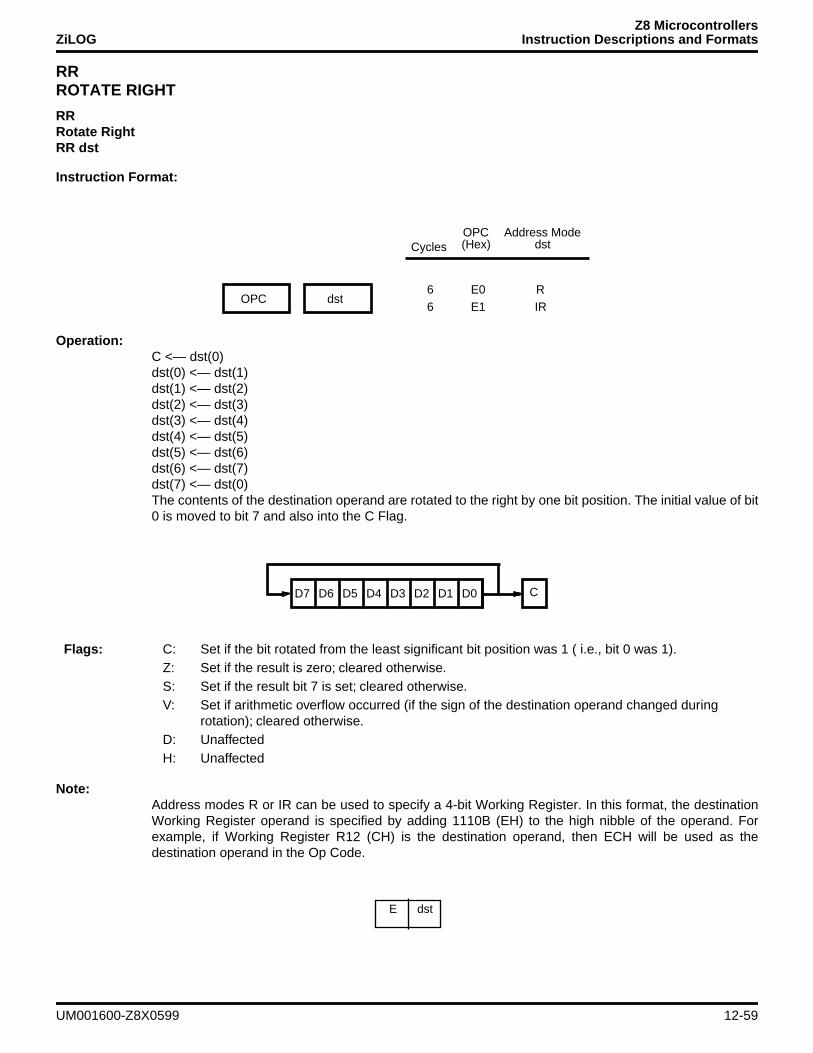
Z8 MicrocontrollersZiLOG Instruction Descriptions and Formats
RRROTATE RIGHT
RRRotate RightRR dst
Instruction Format:
Operation:C <— dst(0)dst(0) <— dst(1)dst(1) <— dst(2)dst(2) <— dst(3)dst(3) <— dst(4)dst(4) <— dst(5)dst(5) <— dst(6)dst(6) <— dst(7)dst(7) <— dst(0)The contents of the destination operand are rotated to the right by one bit position. The initial value of bit0 is moved to bit 7 and also into the C Flag.
Note:Address modes R or IR can be used to specify a 4-bit Working Register. In this format, the destinationWorking Register operand is specified by adding 1110B (EH) to the high nibble of the operand. Forexample, if Working Register R12 (CH) is the destination operand, then ECH will be used as thedestination operand in the Op Code.
OPC dst6
CyclesOPC(Hex)
Address Modedst
E0 R6 E1 IR
D7 D6 D5 D4 D3 D2 D1 D0 C
Flags: C: Set if the bit rotated from the least significant bit position was 1 ( i.e., bit 0 was 1).Z: Set if the result is zero; cleared otherwise.S: Set if the result bit 7 is set; cleared otherwise.V: Set if arithmetic overflow occurred (if the sign of the destination operand changed during
rotation); cleared otherwise.D: UnaffectedH: Unaffected
E dst
UM001600-Z8X0599 12-59
Z8 MicrocontrollersInstruction Descriptions and Formats ZiLOG
RRROTATE RIGHT
Example:If the contents of Working Register R6 are 31H (00110001B), the statement:
RR R6Op Code: E0 E6
leaves the value 98H (10011000) in Working Register R6. The C, V, and S Flags are set, and the Z Flagis cleared.
Example:If the contents of Register C6 are 31H and the contents of Register 31H are 7EH (01111110B), thestatement:
RR @C6Op Code: E1 C6
leaves the value 4FH (00111111) in Register 31H. The C, Z, V, and S Flags are cleared.
12-60 UM001600-Z8X0599
Z8 MicrocontrollersZiLOG Instruction Descriptions and Formats
RRCROTATE RIGHT THROUGH CARRY
RRCRotate Right Through CarryRRC dst
Instruction Format:
Operation:C <— dst(0)dst(0) <— dst(1)dst(1) <— dst(2)dst(2) <— dst(3)dst(3) <— dst(4)dst(4) <— dst(5)dst(5) <— dst(6)dst(6) <— dst(7)dst(7) <— CThe contents of the destination operand with the C Flag are rotated right by one bit position. The initialvalue of bit 0 replaces the C Flag and the initial value of the C Flag replaces bit 7.
Note:Address modes R or IR can be used to specify a 4-bit Working Register. In this format, the destinationWorking Register operand is specified by adding 1110B (EH) to the high nibble of the operand. Forexample, if Working Register R12 (CH) is the destination operand, then ECH will be used as thedestination operand in the Op Code.
OPC dst6
CyclesOPC(Hex)
Address Modedst
C0 R6 C1 IR
D7 D6 D5 D4 D3 D2 D1 D0 C
Flags: C: Set if the bit rotated from the least significant bit position was 1 (i.e., bit 0 was 1).Z: Set if the result is zero; cleared otherwise.S: Set if the result bit 7 is set; cleared otherwise.V: Set if arithmetic overflow occurred (if the sign of the destination operand changed during
rotation); cleared otherwise.D: UnaffectedH: Unaffected
E dst
UM001600-Z8X0599 12-61
Z8 MicrocontrollersInstruction Descriptions and Formats ZiLOG
RRCROTATE RIGHT THROUGH CARRY
Example:If the contents of Register C6H are DDH (11011101B) and the C Flag is reset, the statement:
RRC C6HOp Code: C0 C6
leaves the value 6EH (01101110B) in register C6H. The C and V Flags are set, and the Z and S Flagsare cleared.
Example:If the contents of Register 2C are EDH, the contents of Register EDH is 00H (00000000B), and the CFlag is reset, the statement:
RRC @2CHOp Code: C1 2C
leaves the value 02H (00000010B) in Register EDH. The C, Z, S, and V Flags are reset.
12-62 UM001600-Z8X0599
Z8 MicrocontrollersZiLOG Instruction Descriptions and Formats
SBCSUBTRACT WITH CARRY
SBCSubtract With CarrySBC dst, src
Instruction Format:
Operation:dst <— dst - src - CThe source operand, along with the setting of the C Flag, is subtracted from the destination operand andthe result is stored in the destination operand. The contents of the source operand are not affected.Subtraction is performed by adding the two’s complement of the source operand to the destinationoperand. In multiple precision arithmetic, this instruction permits the carry (borrow) from the subtractionof low order operands to be subtracted from the subtraction of high order operands.
Note:Address modes R or IR can be used to specify a 4-bit Working Register. In this format, the source ordestination Working Register operand is specified by adding 1110B (EH) to the high nibble of theoperand. For example, if Working Register R12 (CH) is the destination operand, then ECH will be usedas the destination operand in the Op Code.
dst srcOPC
OPC
OPC
src
dst
dst
src
6
CyclesOPC(Hex)
Addressdst
Modesrc
32 r r6 33 r Ir
10 34 R R10 35 R IR
10 36 R IM10 37 IR IM
Flags: C: Cleared if there is a carry from the most significant bit of the result; set otherwise, indicating a “borrow.”
Z: Set if the result is 0; cleared otherwise.V: Set if arithmetic overflow occurred (if the operands were of opposite sign and the sign of the
result is the same as the sign of the source); reset otherwise.S: Set if the result is negative; cleared otherwise.H: Cleared if there is a carry from the most significant bit of the low order four bits of the result;
set otherwise indicating a “borrow.”D: Always set to 1.
E src E dstor
UM001600-Z8X0599 12-63
Z8 MicrocontrollersInstruction Descriptions and Formats ZiLOG
SBCSUBTRACT WITH CARRY
Example: Working Register R3 contains 16H, the C Flag is set to 1, and Working Register R11 contains 20H, thestatement:
SBC R3, R11Op Code: 32 3B
leaves the value F5H in Working Register R3. The C, S, and D Flags are set, and the Z, V, and H Flagsare all cleared.
Example:If Working Register R15 contains 16H, the C Flag is not set, Working Register R10 contains 20H, andRegister 20H contains 11H, the statement:
SBC R16, @R10Op Code: 33 FA
leaves the value 05H in Working Register R15. The D Flag is set, and the C, Z, S, V, and H Flags arecleared.
Example:If Register 34H contains 2EH, the C Flag is set, and Register 12H contains 1BH, the statement:
SBC 34H, 12HOp Code: 34 12 34
leaves the value 13H in Register 34H. The D Flag is set, and the C, Z, S, V, and H Flags are cleared.
Example:If Register 4BH contains 82H, the C Flag is set, Working Register R3 contains 10H, and Register 10Hcontains 01H, the statement:
SBC 4BH, @R3Op Code: 35 E3 4B
leaves the value 80H in Register 4BH. The D Flag is set, and the C, Z, S, V, and H Flags are cleared.
Example:If Register 6CH contains 2AH, and the C Flag is not set, the statement:
SBC 6CH, #03HOp Code: 36 6C 03
leaves the value 27H in Register 6CH. The D Flag is set, and the C, Z, S, V, and H Flags are cleared.
Example:If Register D4H contains 5FH, Register 5FH contains 4CH, and the C Flag is set, the statement:
SBC @D4H, #02HOp Code: 37 D4 02
leaves the value 4AH in Register 5FH. The D Flag is set, and the C, Z, S, V, and H Flags are cleared.
12-64 UM001600-Z8X0599
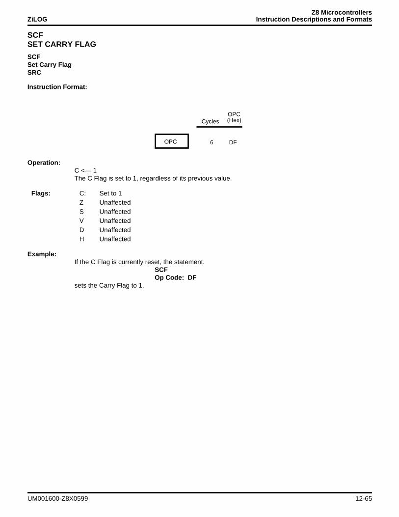
Z8 MicrocontrollersZiLOG Instruction Descriptions and Formats
SCFSET CARRY FLAG
SCFSet Carry FlagSRC
Instruction Format:
Operation:C <— 1The C Flag is set to 1, regardless of its previous value.
Example:If the C Flag is currently reset, the statement:
SCFOp Code: DF
sets the Carry Flag to 1.
OPC 6
CyclesOPC(Hex)
DF
Flags: C: Set to 1Z UnaffectedS UnaffectedV UnaffectedD UnaffectedH Unaffected
UM001600-Z8X0599 12-65
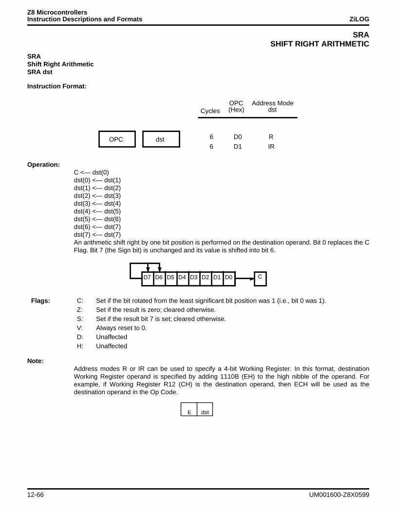
Z8 MicrocontrollersInstruction Descriptions and Formats ZiLOG
SRASHIFT RIGHT ARITHMETIC
SRAShift Right ArithmeticSRA dst
Instruction Format:
Operation:C <— dst(0)dst(0) <— dst(1)dst(1) <— dst(2)dst(2) <— dst(3)dst(3) <— dst(4)dst(4) <— dst(5)dst(5) <— dst(6)dst(6) <— dst(7)dst(7) <— dst(7)An arithmetic shift right by one bit position is performed on the destination operand. Bit 0 replaces the CFlag. Bit 7 (the Sign bit) is unchanged and its value is shifted into bit 6.
Note:Address modes R or IR can be used to specify a 4-bit Working Register. In this format, destinationWorking Register operand is specified by adding 1110B (EH) to the high nibble of the operand. Forexample, if Working Register R12 (CH) is the destination operand, then ECH will be used as thedestination operand in the Op Code.
OPC dst 6
CyclesOPC(Hex)
Address Modedst
D0 R
6 D1 IR
D7 D6 D5 D4 D3 D2 D1 D0 C
Flags: C: Set if the bit rotated from the least significant bit position was 1 (i.e., bit 0 was 1).Z: Set if the result is zero; cleared otherwise.S: Set if the result bit 7 is set; cleared otherwise.V: Always reset to 0.D: UnaffectedH: Unaffected
E dst
12-66 UM001600-Z8X0599
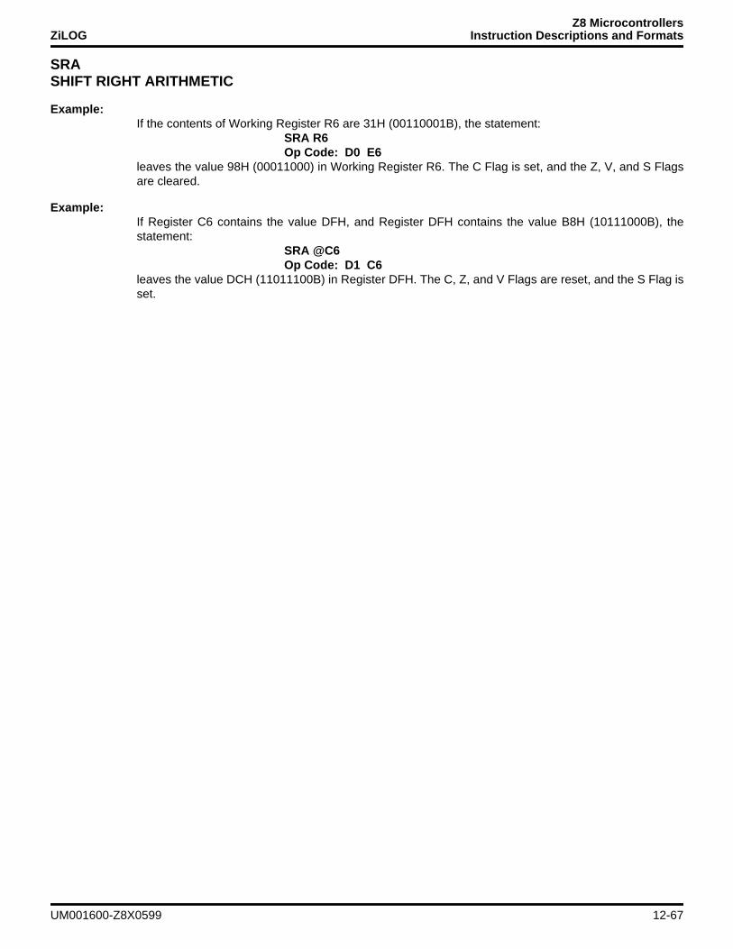
Z8 MicrocontrollersZiLOG Instruction Descriptions and Formats
SRASHIFT RIGHT ARITHMETIC
Example:If the contents of Working Register R6 are 31H (00110001B), the statement:
SRA R6Op Code: D0 E6
leaves the value 98H (00011000) in Working Register R6. The C Flag is set, and the Z, V, and S Flagsare cleared.
Example:If Register C6 contains the value DFH, and Register DFH contains the value B8H (10111000B), thestatement:
SRA @C6Op Code: D1 C6
leaves the value DCH (11011100B) in Register DFH. The C, Z, and V Flags are reset, and the S Flag isset.
UM001600-Z8X0599 12-67
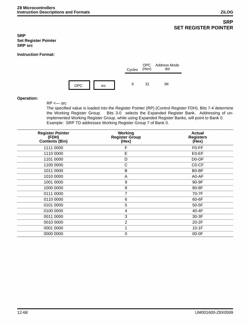
Z8 MicrocontrollersInstruction Descriptions and Formats ZiLOG
SRPSET REGISTER POINTER
SRPSet Register PointerSRP src
Instruction Format:
Operation:RP <— srcThe specified value is loaded into the Register Pointer (RP) (Control Register FDH). Bits 7-4 determinethe Working Register Group. Bits 3-0 selects the Expanded Register Bank. Addressing of un-implemented Working Register Group, while using Expanded Register Banks, will point to Bank 0. Example: SRP TD addresses Working Register Group 7 of Bank 0.
OPC src 6
CyclesOPC(Hex)
Address Modedst
31 IM
Register Pointer Working Actual(FDH) Register Group Registers
Contents (Bin) (Hex) (Hex)
1111 0000 F F0-FF1110 0000 E E0-EF1101 0000 D D0-DF1100 0000 C C0-CF1011 0000 B B0-BF1010 0000 A A0-AF1001 0000 9 90-9F1000 0000 8 80-8F0111 0000 7 70-7F0110 0000 6 60-6F0101 0000 5 50-5F0100 0000 4 40-4F0011 0000 3 30-3F0010 0000 2 20-2F0001 0000 1 10-1F0000 0000 0 00-0F
12-68 UM001600-Z8X0599
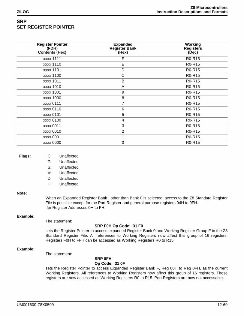
Z8 MicrocontrollersZiLOG Instruction Descriptions and Formats
SRPSET REGISTER POINTER
Note:When an Expanded Register Bank , other than Bank 0 is selected, access to the Z8 Standard RegisterFile is possible except for the Port Register and general purpose registers 04H to 0FH. fpr Register Addresses 0H to FH.
Example:The statement:
SRP F0H Op Code: 31 F0sets the Register Pointer to access expanded Register Bank 0 and Working Register Group F in the Z8Standard Register File. All references to Working Registers now affect this group of 16 registers.Registers F0H to FFH can be accessed as Working Registers R0 to R15
Example:The statement:
SRP 0FHOp Code: 31 0F
sets the Register Pointer to access Expanded Register Bank F, Reg 00H to Reg 0FH, as the currentWorking Registers. All references to Working Registers now affect this group of 16 registers. Theseregisters are now accessed as Working Registers R0 to R15. Port Registers are now not accessable.
Register Pointer Expanded Working(FDH) Register Bank Registers
Contents (Hex) (Hex) (Dec)
xxxx 1111 F R0-R15xxxx 1110 E R0-R15xxxx 1101 D R0-R15xxxx 1100 C R0-R15xxxx 1011 B R0-R15xxxx 1010 A R0-R15xxxx 1001 9 R0-R15xxxx 1000 8 R0-R15xxxx 0111 7 R0-R15xxxx 0110 6 R0-R15xxxx 0101 5 R0-R15xxxx 0100 4 R0-R15xxxx 0011 3 R0-R15xxxx 0010 2 R0-R15xxxx 0001 1 R0-R15xxxx 0000 0 R0-R15
Flags: C: UnaffectedZ: UnaffectedS: UnaffectedV: UnaffectedD: UnaffectedH: Unaffected
UM001600-Z8X0599 12-69
Z8 MicrocontrollersInstruction Descriptions and Formats ZiLOG
SRPSET REGISTER POINTER
Example:Assume the RP currently addresses the Control and Peripheral Working Register Group and the programhas just entered an interrupt service routine. The statement:
SRP 70HOp Code: 31 70
retains the contents of the Control and Peripheral Registers by setting the RP to 70H (01110000B). Anyreference to Working Registers in the interrupt routine will point to registers 70H to 7FH.
12-70 UM001600-Z8X0599
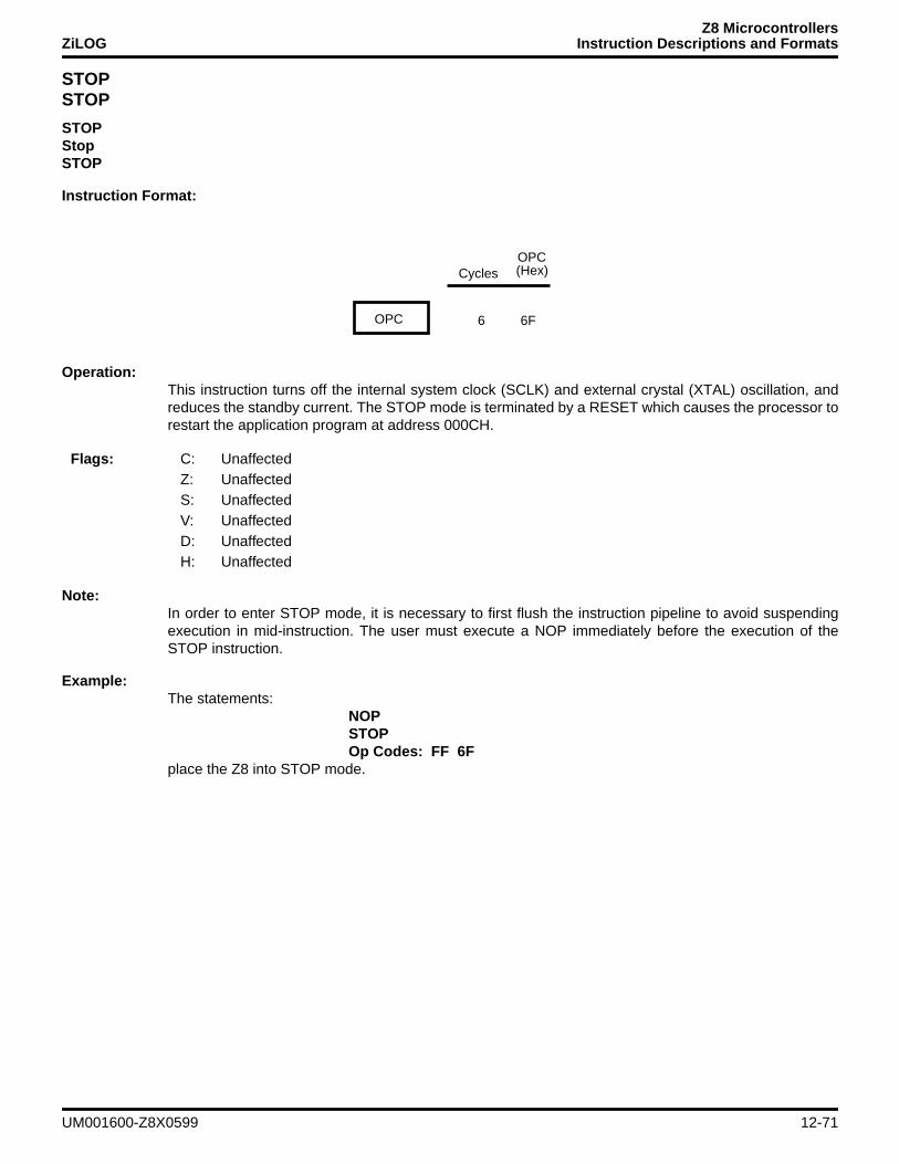
Z8 MicrocontrollersZiLOG Instruction Descriptions and Formats
STOPSTOP
STOPStopSTOP
Instruction Format:
Operation:This instruction turns off the internal system clock (SCLK) and external crystal (XTAL) oscillation, andreduces the standby current. The STOP mode is terminated by a RESET which causes the processor torestart the application program at address 000CH.
Note:In order to enter STOP mode, it is necessary to first flush the instruction pipeline to avoid suspendingexecution in mid-instruction. The user must execute a NOP immediately before the execution of theSTOP instruction.
Example:The statements:
NOPSTOPOp Codes: FF 6F
place the Z8 into STOP mode.
OPC 6
CyclesOPC(Hex)
6F
Flags: C: UnaffectedZ: UnaffectedS: UnaffectedV: UnaffectedD: UnaffectedH: Unaffected
UM001600-Z8X0599 12-71
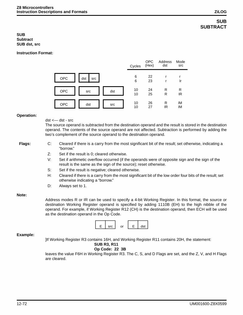
Z8 MicrocontrollersInstruction Descriptions and Formats ZiLOG
SUBSUBTRACT
SUBSubtractSUB dst, src
Instruction Format:
Operation:dst <— dst - srcThe source operand is subtracted from the destination operand and the result is stored in the destinationoperand. The contents of the source operand are not affected. Subtraction is performed by adding thetwo’s complement of the source operand to the destination operand.
Note:Address modes R or IR can be used to specify a 4-bit Working Register. In this format, the source ordestination Working Register operand is specified by adding 1110B (EH) to the high nibble of theoperand. For example, if Working Register R12 (CH) is the destination operand, then ECH will be usedas the destination operand in the Op Code.
Example:]If Working Register R3 contains 16H, and Working Register R11 contains 20H, the statement:
SUB R3, R11Op Code: 22 3B
leaves the value F6H in Working Register R3. The C, S, and D Flags are set, and the Z, V, and H Flagsare cleared.
dst srcOPC
OPC
OPC
src
dst
dst
src
6
CyclesOPC(Hex)
Addressdst
Modesrc
22 r r6 23 r Ir
10 24 R R10 25 R IR
10 26 R IM10 27 IR IM
Flags: C: Cleared if there is a carry from the most significant bit of the result; set otherwise, indicating a “borrow.”
Z: Set if the result is 0; cleared otherwise.V: Set if arithmetic overflow occurred (if the operands were of opposite sign and the sign of the
result is the same as the sign of the source); reset otherwise.S: Set if the result is negative; cleared otherwise.H: Cleared if there is a carry from the most significant bit of the low order four bits of the result; set
otherwise indicating a “borrow.”D: Always set to 1.
E src E dstor
12-72 UM001600-Z8X0599
Z8 MicrocontrollersZiLOG Instruction Descriptions and Formats
SUBSUBTRACT
Example:If Working Register R15 contains 16H, Working Register R10 contains 20H, and Register 20H contains11H, the statement:
SUB R16, @R10Op Code: 23 FA
leaves the value 05H in Working Register R15. The D Flag is set, and the C, Z, S, V, and H Flags arecleared.
Example:If Register 34H contains 2EH, and Register 12H contains 1BH, the statement:
SUB 34H, 12HOp Code: 24 12 34
leaves the value 13H in Register 34H. The D Flag is set, and the C, Z, S, V, and H Flags are cleared.
Example:If Register 4BH contains 82H, Working Register R3 contains 10H, and Register 10H contains 01H, thestatement:
SUB 4BH, @R3Op Code: 25 E3 4B
leaves the value 81H in Register 4BH. The D Flag is set, and the C, Z, S, V, and H Flags are cleared.
Example:If Register 6CH contains 2AH, the statement:
SUB 6CH, #03HOp Code: 26 6C 03
leaves the value 27H in Register 6CH. The D Flag is set, and the C, Z, S, V, and H Flags are cleared.
Example:If Register D4H contains 5FH, Register 5FH contains 4CH, the statement:
SUB @D4H, #02HOp Code: 17 D4 02
leaves the value 4AH in Register 5FH. The D Flag is set, and the C, Z, S, V, and H Flags are cleared.
UM001600-Z8X0599 12-73
Z8 MicrocontrollersInstruction Descriptions and Formats ZiLOG
SWAPSWAP NIBBLES
SWAPSwap NibblesSWAP dst
Instruction Format:
Operation:dst(7-4) <—> dst(3-0)The contents of the lower four bits and upper four bits of the destination operand are swapped.
Note:Address modes R or IR can be used to specify a 4-bit Working Register. In this format, destinationWorking Register operand is specified by adding 1110B (EH) to the high nibble of the operand. Forexample, if Working Register R12 (CH) is the destination operand, then ECH will be used as thedestination operand in the Op Code.
Example:If Register BCH contains B3H (10110011B), the statement:
SWAP B3HOp Code: F0 B3
will leave the value 3BH (00111011B) in Register BCH. The Z and S Flags are cleared.
Example:If Working Register R5 contains BCH and Register BCH contains B3H (10110011B), the statement:
SWAP @R5HOp Code: F1 E5
will leave the value 3BH (00111011B) in Register BCH. The Z and S Flags are cleared.
Flags: C: UnaffectedZ: Set if the result is zero; cleared otherwise.S: Set if the result bit 7 is set; cleared otherwise.V: UndefinedD: UnaffectedH: Unaffected
OPC dst 6
CyclesOPC(Hex)
Address Modedst
F0 R6 F1 IR
E dst
12-74 UM001600-Z8X0599
Z8 MicrocontrollersZiLOG Instruction Descriptions and Formats
TCMTEST COMPLEMENT UNDER MASK
TCMTest Complement Under MaskTCM dst, src
Instruction Format:
Operation:(NOT dst) AND srcThis instruction tests selected bits in the destination operand for a logical 1 value. The bits to be testedare specified by setting a 1 bit in the corresponding bit position in the source operand (the mask). TheTCM instruction complements the destination operand, and then ANDs it with the source mask(operand). The Zero (Z) Flag can then be checked to determine the result. If the Z Flag is set, then thetested bits were 1. When the TCM operation is complete, the destination and source operands stillcontain their original values.
Note:Address modes R or IR can be used to specify a 4-bit Working Register. In this format, the source ordestination Working Register operand is specified by adding 1110B (EH) to the high nibble of theoperand. For example, if Working Register R12 (CH) is the destination operand, then ECH will be usedas the destination operand in the Op Code.
dst srcOPC
OPC
OPC
src
dst
dst
src
6
CyclesOPC(Hex)
Addressdst
Modesrc
62 r r6 63 r Ir
10 64 R R10 65 R IR
10 66 R IM10 67 IR IM
Flags : C: UnaffectedZ: Set if the result is zero; cleared otherwise.S: Set if the result bit 7 is set; cleared otherwise.V: Always reset to 0.D: UnaffectedH: Unaffected
E src E dstor
UM001600-Z8X0599 12-75
Z8 MicrocontrollersInstruction Descriptions and Formats ZiLOG
TCMTEST COMPLEMENT UNDER MASK
Example:If Working Register R3 contains 45H (01000101B) and Working Register R7 contains the value 01H(00000001B) (bit 0 is being tested if it is 1), the statement:
TCM R3, R7Op Code: 62 37
will set the Z Flag indicating bit 0 in the destination operand is 1. The V and S Flags are cleared.
Example:If Working Register R14 contains the value F3H (11110011B), Working Register R5 contains CBH, andRegister CBH contains 88H (10001000B) (bit 7 and bit 3 are being tested if they are 1), the statement:
TCM R14, @R5Op Code: 63 E5
will reset the Z Flag, because bit 3 in the destination operand is not a 1. The V and S Flags are alsocleared.
Example:If Register D4H contains the value 04H (000001000B), and Working Register R0 contains the value 80H(10000000B) (bit 7 is being tested if it is 1), the statement:
TCM D4H, R0Op Code: 64 E0 D4
will reset the Z Flag, because bit 7 in the destination operand is not a 1. The S Flag will be set, and theV Flag will be cleared.
Example:If Register DFH contains the value FFH (11111111B), Register 07H contains the value 1FH, and Register1FH contains the value BDH (10111101B) (bit 7, bit 5, bit 4, bit 3, bit 2, and bit 0 are being tested if theyare 1), the statement:
TCM DFH, @07HOp Code: 65 07 DF
will set the Z Flag indicating the tested bits in the destination operand are 1. The S and V Flags arecleared.
Example:If Working Register R13 contains the value F2H (11110010B), the statement:
TCM R13, #02HOp Code: 66 ED, 02
tests bit 1 of the destination operand for 1. The Z Flag will be set indicating bit 1 in the destination operandwas 1. The S and V Flags are cleared.
Example:If Register 5DH contains A0H, and Register A0H contains 0FH (00001111B), the statement:
TCM @5D, #10HOp Code: 67 5D 10
tests bit 4 of the Register A0H for 1. The Z Flag will be reset indicating bit 1 in the destination operandwas not 1. The S and V Flags are cleared.
12-76 UM001600-Z8X0599
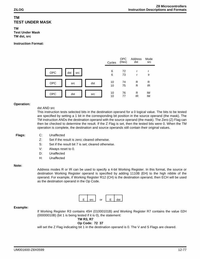
Z8 MicrocontrollersZiLOG Instruction Descriptions and Formats
TMTEST UNDER MASK
TMTest Under MaskTM dst, src
Instruction Format:
Operation:dst AND srcThis instruction tests selected bits in the destination operand for a 0 logical value. The bits to be testedare specified by setting a 1 bit in the corresponding bit position in the source operand (the mask). TheTM instruction ANDs the destination operand with the source operand (the mask). The Zero (Z) Flag canthen be checked to determine the result. If the Z Flag is set, then the tested bits were 0. When the TMoperation is complete, the destination and source operands still contain their original values.
Note:Address modes R or IR can be used to specify a 4-bit Working Register. In this format, the source ordestination Working Register operand is specified by adding 1110B (EH) to the high nibble of theoperand. For example, if Working Register R12 (CH) is the destination operand, then ECH will be usedas the destination operand in the Op Code.
Example:If Working Register R3 contains 45H (01000101B) and Working Register R7 contains the value 02H(00000010B) (bit 1 is being tested if it is 0), the statement:
TM R3, R7Op Code: 72 37
will set the Z Flag indicating bit 1 in the destination operand is 0. The V and S Flags are cleared.
dst srcOPC
OPC
OPC
src
dst
dst
src
6
CyclesOPC(Hex)
Addressdst
Modesrc
72 r r6 73 r Ir
10 74 R R10 75 R IR
10 76 R IM10 77 IR IM
Flags: C: UnaffectedZ: Set if the result is zero; cleared otherwise.S: Set if the result bit 7 is set; cleared otherwise.V: Always reset to 0.D: UnaffectedH: Unaffected
E src E dstor
UM001600-Z8X0599 12-77
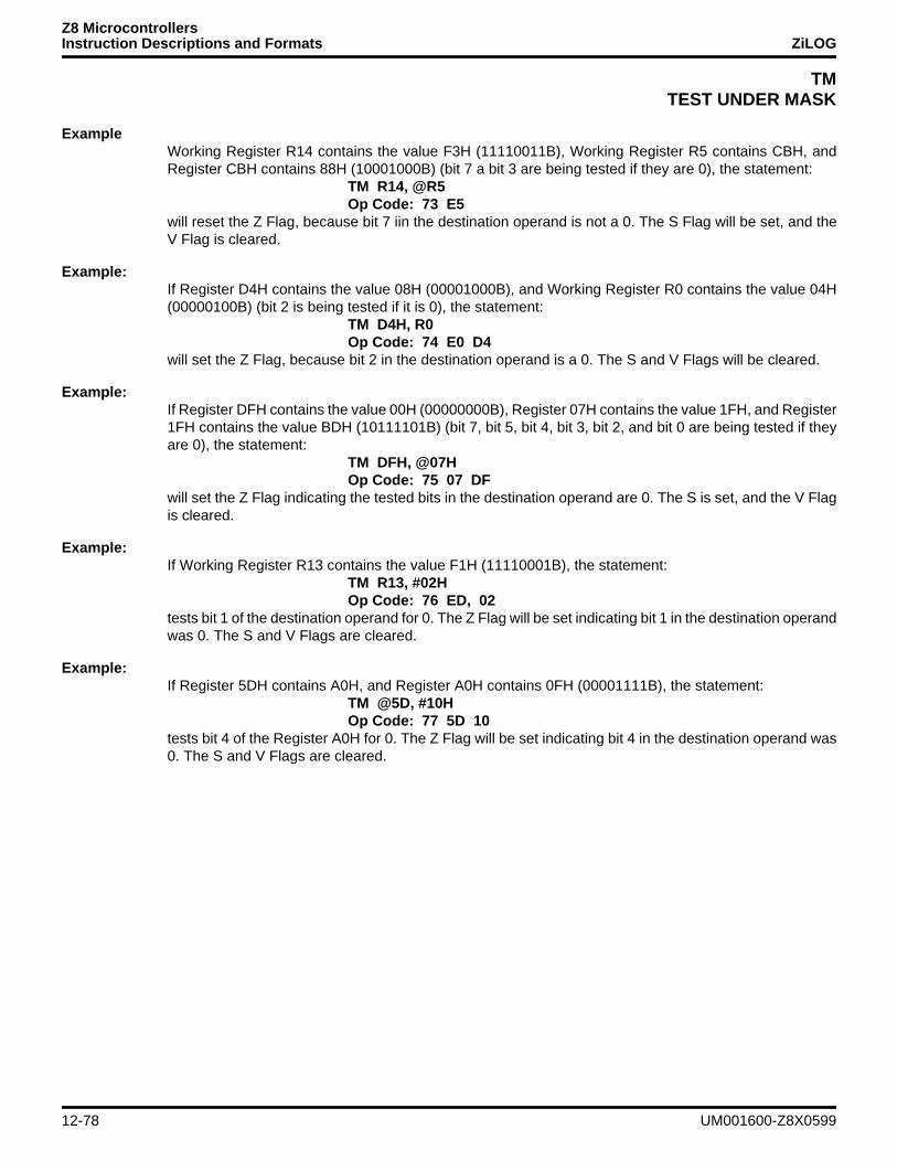
Z8 MicrocontrollersInstruction Descriptions and Formats ZiLOG
TMTEST UNDER MASK
ExampleWorking Register R14 contains the value F3H (11110011B), Working Register R5 contains CBH, andRegister CBH contains 88H (10001000B) (bit 7 a bit 3 are being tested if they are 0), the statement:
TM R14, @R5Op Code: 73 E5
will reset the Z Flag, because bit 7 iin the destination operand is not a 0. The S Flag will be set, and theV Flag is cleared.
Example:If Register D4H contains the value 08H (00001000B), and Working Register R0 contains the value 04H(00000100B) (bit 2 is being tested if it is 0), the statement:
TM D4H, R0Op Code: 74 E0 D4
will set the Z Flag, because bit 2 in the destination operand is a 0. The S and V Flags will be cleared.
Example:If Register DFH contains the value 00H (00000000B), Register 07H contains the value 1FH, and Register1FH contains the value BDH (10111101B) (bit 7, bit 5, bit 4, bit 3, bit 2, and bit 0 are being tested if theyare 0), the statement:
TM DFH, @07HOp Code: 75 07 DF
will set the Z Flag indicating the tested bits in the destination operand are 0. The S is set, and the V Flagis cleared.
Example:If Working Register R13 contains the value F1H (11110001B), the statement:
TM R13, #02HOp Code: 76 ED, 02
tests bit 1 of the destination operand for 0. The Z Flag will be set indicating bit 1 in the destination operandwas 0. The S and V Flags are cleared.
Example:If Register 5DH contains A0H, and Register A0H contains 0FH (00001111B), the statement:
TM @5D, #10HOp Code: 77 5D 10
tests bit 4 of the Register A0H for 0. The Z Flag will be set indicating bit 4 in the destination operand was0. The S and V Flags are cleared.
12-78 UM001600-Z8X0599
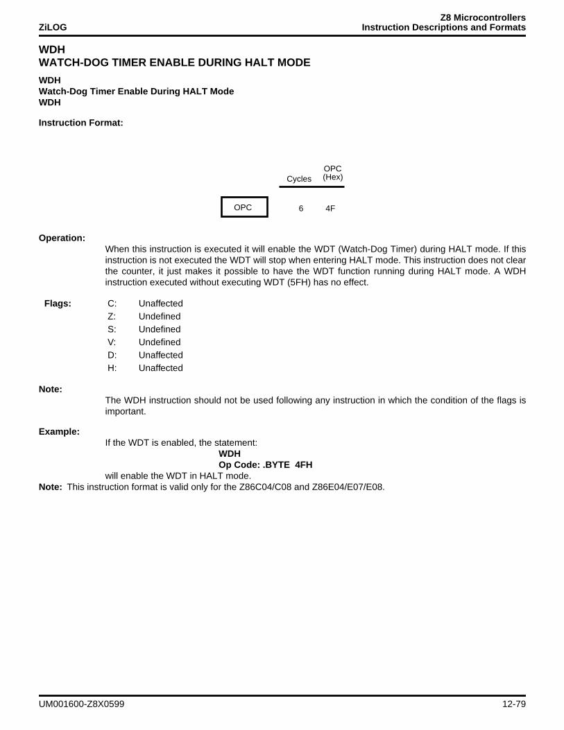
Z8 MicrocontrollersZiLOG Instruction Descriptions and Formats
WDHWATCH-DOG TIMER ENABLE DURING HALT MODE
WDHWatch-Dog Timer Enable During HALT ModeWDH
Instruction Format:
Operation:When this instruction is executed it will enable the WDT (Watch-Dog Timer) during HALT mode. If thisinstruction is not executed the WDT will stop when entering HALT mode. This instruction does not clearthe counter, it just makes it possible to have the WDT function running during HALT mode. A WDHinstruction executed without executing WDT (5FH) has no effect.
Note:The WDH instruction should not be used following any instruction in which the condition of the flags isimportant.
Example:If the WDT is enabled, the statement:
WDHOp Code: .BYTE 4FH
will enable the WDT in HALT mode.Note: This instruction format is valid only for the Z86C04/C08 and Z86E04/E07/E08.
OPC 6
CyclesOPC(Hex)
4F
Flags: C: UnaffectedZ: UndefinedS: UndefinedV: UndefinedD: UnaffectedH: Unaffected
UM001600-Z8X0599 12-79
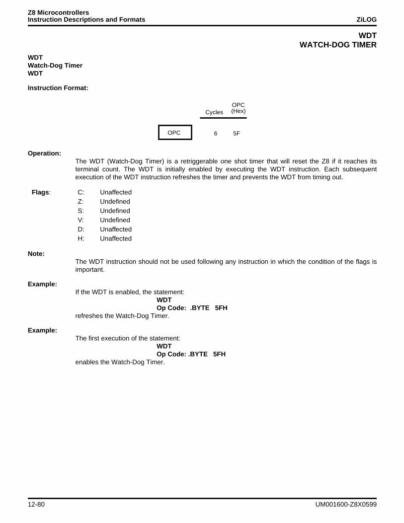
Z8 MicrocontrollersInstruction Descriptions and Formats ZiLOG
WDTWATCH-DOG TIMER
WDTWatch-Dog TimerWDT
Instruction Format:
Operation:The WDT (Watch-Dog Timer) is a retriggerable one shot timer that will reset the Z8 if it reaches itsterminal count. The WDT is initially enabled by executing the WDT instruction. Each subsequentexecution of the WDT instruction refreshes the timer and prevents the WDT from timing out.
Note:The WDT instruction should not be used following any instruction in which the condition of the flags isimportant.
Example:If the WDT is enabled, the statement:
WDTOp Code: .BYTE 5FH
refreshes the Watch-Dog Timer.
Example:The first execution of the statement:
WDTOp Code: .BYTE 5FH
enables the Watch-Dog Timer.
OPC 6
CyclesOPC(Hex)
5F
Flags : C: UnaffectedZ: UndefinedS: UndefinedV: UndefinedD: UnaffectedH: Unaffected
12-80 UM001600-Z8X0599
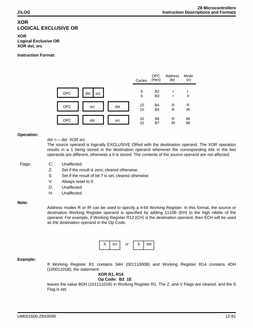
Z8 MicrocontrollersZiLOG Instruction Descriptions and Formats
XORLOGICAL EXCLUSIVE OR
XORLogical Exclusive ORXOR dst, src
Instruction Format:
Operation:dst <— dst XOR src The source operand is logically EXCLUSIVE ORed with the destination operand. The XOR operationresults in a 1 being stored in the destination operand whenever the corresponding bits in the twooperands are different, otherwise a 0 is stored. The contents of the source operand are not affected.
Note:Address modes R or IR can be used to specify a 4-bit Working Register. In this format, the source ordestination Working Register operand is specified by adding 1110B (EH) to the high nibble of theoperand. For example, if Working Register R12 (CH) is the destination operand, then ECH will be usedas the destination operand in the Op Code.
Example:If Working Register R1 contains 34H (00111000B) and Working Register R14 contains 4DH(10001101B), the statement:
XOR R1, R14Op Code: B2 1E
leaves the value BDH (10111101B) in Working Register R1. The Z, and V Flags are cleared, and the SFlag is set.
dst srcOPC
OPC
OPC
src
dst
dst
src
6
CyclesOPC(Hex)
Addressdst
Modesrc
B2 r r6 B3 r Ir
10 B4 R R10 B5 R IR
10 B6 R IM10 B7 IR IM
Flags: C: UnaffectedZ: Set if the result is zero; cleared otherwise.S: Set if the result of bit 7 is set; cleared otherwise.V: Always reset to 0D: UnaffectedH: Unaffected
E src E dstor
UM001600-Z8X0599 12-81
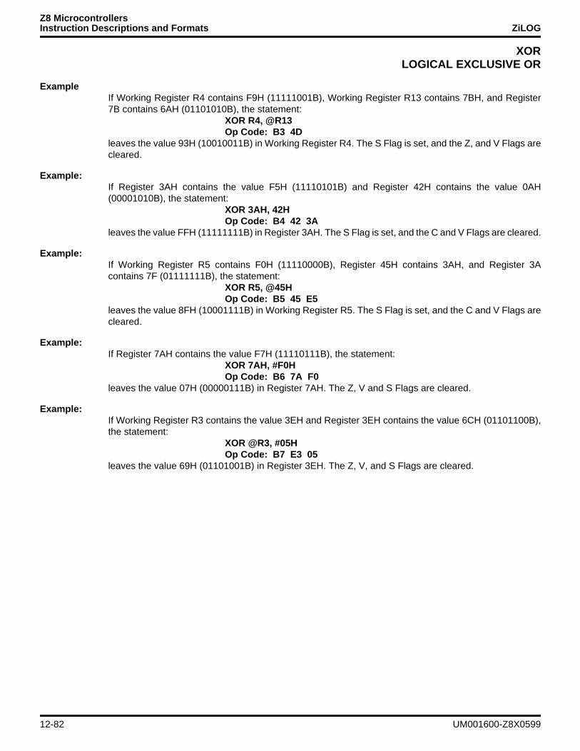
Z8 MicrocontrollersInstruction Descriptions and Formats ZiLOG
XORLOGICAL EXCLUSIVE OR
ExampleIf Working Register R4 contains F9H (11111001B), Working Register R13 contains 7BH, and Register7B contains 6AH (01101010B), the statement:
XOR R4, @R13Op Code: B3 4D
leaves the value 93H (10010011B) in Working Register R4. The S Flag is set, and the Z, and V Flags arecleared.
Example:If Register 3AH contains the value F5H (11110101B) and Register 42H contains the value 0AH(00001010B), the statement:
XOR 3AH, 42HOp Code: B4 42 3A
leaves the value FFH (11111111B) in Register 3AH. The S Flag is set, and the C and V Flags are cleared.
Example:If Working Register R5 contains F0H (11110000B), Register 45H contains 3AH, and Register 3Acontains 7F (01111111B), the statement:
XOR R5, @45HOp Code: B5 45 E5
leaves the value 8FH (10001111B) in Working Register R5. The S Flag is set, and the C and V Flags arecleared.
Example:If Register 7AH contains the value F7H (11110111B), the statement:
XOR 7AH, #F0HOp Code: B6 7A F0
leaves the value 07H (00000111B) in Register 7AH. The Z, V and S Flags are cleared.
Example:If Working Register R3 contains the value 3EH and Register 3EH contains the value 6CH (01101100B),the statement:
XOR @R3, #05HOp Code: B7 E3 05
leaves the value 69H (01101001B) in Register 3EH. The Z, V, and S Flags are cleared.
12-82 UM001600-Z8X0599