z1501d active antenna - okdxf.eu instruction manual-01.pdf · z1501d active antenna” may be...
TRANSCRIPT

Z1501D Active Antenna
Assembly and Operation Manual
Revised 08 September 2010
Clifton Laboratories
7236 Clifton Road
Clifton, VA 20124
(703) 830 0368
www.cliftonlaboratories.com

Z1501D Construction and Operations Manual Page 1
Model Z1501D Active Antenna
Revised 08 September 2010
(c) 2010, 2009 Jack R. Smith d/b/a/ Clifton Laboratories.
Trademarks and Copyright
Material in this document copyrighted © 2009, 2010 Clifton Laboratories. All rights reserved. It is
provided to allow the Z1501D purchasers to maintain their equipment and such other purposes as
may not be prohibited by law.
Warranty
This warranty is effective as of the date of first consumer purchase.
What is covered: During the ninety (90) days after date of purchase, Clifton Laboratories will
correct any defects in the Z1501D due to defective parts (kit or assembled) or workmanship (if
purchased as an assembled unit) free of charge (post-paid). You must send the unit at your expense
to Clifton Laboratories, but we will pay return shipping. Clifton Laboratories’ warranty does not
extend to defects caused by your incorrect assembly or use of unauthorized parts or materials or
construction practices.
What is not covered: If the Z1501D is purchased as a kit, this warranty does not cover correction
of assembly errors or misalignment; repair of damage caused by misuse, negligence, or builder
modifications; or any performance malfunctions involving non-Clifton Laboratories accessory
equipment. The use of acid-core solder, water-soluble flux solder, or any corrosive or conductive flux
or solvent will void this warranty in its entirety. Whether purchased as an assembled unit or as a kit,
also not covered is reimbursement for loss of use, inconvenience, customer assembly or alignment
time, or cost of unauthorized service. Damage due to operating the Z1501D near a transmitting
antenna is not covered under the warranty.
Limitation of incidental or consequential damages: This warranty does not extend to non-
Clifton Laboratories equipment or components used in conjunction with our products. Any such
repair or replacement is the responsibility of the customer. Clifton Laboratories will not be liable for
any special, indirect, incidental or consequential damages, including but not limited to any loss of
business or profits.
Under no circumstances is Clifton Laboratories liable for damage to your equipment
connected to the Z1501D resulting from use of the Z1501D, whether in accordance with the
instructions in this Manual or otherwise.

Z1501D Construction and Operations Manual Page 2
Contents Model Z1501D Active Antenna .......................................................................................................................................... 1
1. Safety Information ......................................................................................................................................................... 3
Typical Antenna Location ................................................................................................................................................ 4
General Safety Rules .......................................................................................................................................................... 4
Equipment Cautions .......................................................................................................................................................... 5
2. General Information and Specifications ............................................................................................................... 6
Description ............................................................................................................................................................................ 6
Specifications ........................................................................................................................................................................ 6
Typical Frequency Response .................................................................................................................................... 7
3. Assembly ........................................................................................................................................................................... 8
Stage 1 ..................................................................................................................................................................................... 8
Stage 2 ................................................................................................................................................................................... 13
Stage 3 ................................................................................................................................................................................... 15
Installation in the enclosure ......................................................................................................................................... 18
4. Installation ...................................................................................................................................................................... 30
Mechanical and Safety Issues ...................................................................................................................................... 30
Whip Length and Selection ........................................................................................................................................... 31
Electrical Noise Pickup ................................................................................................................................................... 31
5. Schematic, Theory of Operation and Troubleshooting ................................................................................ 33
Schematic ........................................................................................................................................................................ 33
Theory of Operation.................................................................................................................................................... 34
Troubleshooting ........................................................................................................................................................... 35
Stage Gain Data ............................................................................................................................................................. 37
6. Parts Provided ............................................................................................................................................................... 38
Appendix A – Adjusting R2 for Optimum 2nd Order Intermodulation Performance ................................. 47
Adjustment Service. ......................................................................................................................................................... 47
Simplified Adjustment Procedure .............................................................................................................................. 47
Full Performance Verification ..................................................................................................................................... 52
Appendix B – Typical Phase Shift amongst Multiple Z1501D and Z1203A Units ....................................... 54

Z1501D Construction and Operations Manual Page 3
1. Safety Information
Installation of the Z1501D near power lines is dangerous and should not be attempted. For your safety follow the installation directions. Before starting installation, plan ahead and decide if your proposed installation location is safe. Installing an antenna such as the Z1501D can be hazardous for several reasons, including, but not limited to:
Most importantly, part of the antenna system, including the supporting mast, may come in contact with electric power lines.
You may fall off the roof if installing the Z1501D on a roof mount. If installing a supporting mast, you may find buried power lines or gas lines or other
dangerous hidden obstructions.
Z1501D Construction and Operations Manual Page 4
Even momentary contact between a power line and any part of the antenna system can be instantly fatal. Falling off the roof can easily cause serious injury or death. Unfortunately, every year people are injured or killed installing antennas. These accidents can be prevented by first identifying a safe location for your antenna and then following good safety practices during the installation.
Typical Antenna Location
A major advantage of active antennas such as the Z1501D is that they work well when installed
near the ground. Mounting the Z1501D on a tall mast or tower is not necessary and won’t improve
performance. Clifton Laboratories recommends using a support mast of four to eight feet in length.
Taller masts are not necessary and will increase the risk of danger when installing the Z1501D.
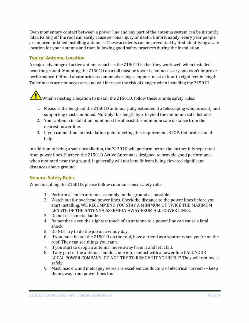
When selecting a location to install the Z1501D, follow these simple safety rules:
1. Measure the length of the Z1501D antenna (fully extended if a telescoping whip is used) and
supporting mast combined. Multiply this length by 2 to yield the minimum safe distance.
2. Your antenna installation point must be at least this minimum safe distance from the
nearest power line.
3. If you cannot find an installation point meeting this requirement, STOP. Get professional
help.
In addition to being a safer installation, the Z1501D will perform better the further it is separated
from power lines. Further, the Z1501D Active Antenna is designed to provide good performance
when mounted near the ground. It generally will not benefit from being elevated significant
distances above ground.
General Safety Rules
When installing the Z1501D, please follow common sense safety rules:
1. Perform as much antenna assembly on the ground as possible. 2. Watch out for overhead power lines. Check the distance to the power lines before you
start installing. WE RECOMMEND YOU STAY A MINIMUM OF TWICE THE MAXIMUM LENGTH OF THE ANTENNA ASSEMBLY AWAY FROM ALL POWER LINES.
3. Do not use a metal ladder. 4. Remember, even the slightest touch of an antenna to a power line can cause a fatal
shock. 5. Do NOT try to do the job on a windy day. 6. If you must install the Z1501D on the roof, have a friend as a spotter when you’re on the
roof. They can see things you can’t. 7. If you start to drop an antenna, move away from it and let it fall. 8. If any part of the antenna should come into contact with a power line CALL YOUR
LOCAL POWER COMPANY! DO NOT TRY TO REMOVE IT YOURSELF! They will remove it safely.
9. Mast, lead-in, and metal guy wires are excellent conductors of electrical current - - keep them away from power lines too.

Z1501D Construction and Operations Manual Page 5
10. Be sure your family and friends understand the danger of touching an overhead power line. Tell them never to try to remove any object in contact with a power line - - CB, TV antenna, or anything else.
11. Make sure that the antenna mast assembly is properly grounded.
It bears repeating. If you have the slightest doubt about your ability to safely install the
Z1501D, do not attempt it. Hire a professional installer. Your life is worth far more than the cost of a
professional installation!
Equipment Cautions
The Z1501D operates with a user-supplied DC power supply of 13.8V (nominal) duplexed over the
coaxial cable that carries the signal. The DC power may be coupled using Clifton Laboratories model
Z1203A Active Antenna Power Coupler or similar device. Note that by design, therefore, the
Z1501’s coaxial cable has DC voltage on it. If inadvertently connected to a receiver or similar device,
excess current may flow and damage the receiver or other device. It is the user’s responsibility to
ensure that a suitable power coupler is used and that the coupler is properly connected to the
remote active antenna and the receiver.
The Z1501D has no fuse; it depends upon the power coupler having a suitable design to limit short
circuit current.
The Z1501D is designed to be operated in areas of moderate electromagnetic fields, including
typical amateur radio transmitters where the Z1501D is located a reasonable distance from
transmitting antennas. It is possible to damage the Z1501D by operating in close proximity to a
transmitting antenna. Damage due to operating the Z1501D near a transmitting antenna is not
covered under the warranty.

Z1501D Construction and Operations Manual Page 6
2. General Information and Specifications
Description
The Z1501D is an electric field responding “active” antenna. The Z1501D employs a high impedance
field effect transistor input stage to efficiently couple electromagnetic field from a physically short
antenna to a low impedance (50 ohms) load.
The Z1501D is based, in part, upon a design by Chris Trask, N7ZWY, described in “Complementary
Push-Pull Amplifiers for Active Antennas: A Critical Review.” It also incorporates ideas from other
sources as well as extensive optimization work by Clifton Laboratories. The Z1501D modifies
Chris’s design in significant respects:
Improved output stage component values for better intermodulation performance;
Additional buffer amplifier stage to improve intermodulation performance;
Redesigned input stage to improve intermodulation performance;
Improved low frequency response, with usable frequency range extended downward to 20
KHz.
Intentional roll-off at very low frequencies to reduce power line harmonic pickup.
Increased resistance to damage due to strong electromagnetic fields from nearby
transmitters.
Adjustment of input JFET bias to optimize 2nd order intermodulation performance
Specifications
Parameter Value
Dimensions Printed circuit board 2 inches x 3 inches (51 mm x 76 mm); when enclosed in weatherproof enclosure 4.5 inches x 2.5 inches x 1 inch (114 mm x 63 mm x 25 mm) excluding mounting flange.
DC Ratings Voltage not to exceed 15V, negative ground, positive to coaxial cable center conductor. Typical current consumption 100 mA. Performance based on 13.8V delivered to active antenna.
Output impedance Designed to drive 50 ohm coaxial cable; 75 ohm cable may also be used.
Frequency Range 20 KHz – 30 MHz; usable to 100 MHz with reduced performance.
Insertion Loss When measured with 50 ohm termination on input, 2.5 dB typical over range 10 KHz – 30 MHz; not to exceed 3.5 dB, measured with Clifton Laboratories Z1203A power coupler.
3rd Order Intermodulation Intercept
With test tones of 3.007 and 4.011 MHz, adjusted for 0 dBm output from the Z1501D, and a 15 pF/50R whip simulation adapter at the input connector: * 3rd order output intercept (OIP3): +40 dBm.
2nd Order Intermodulation Intercept
With test tones of 3.007 and 4.011 MHz, adjusted for 0 dBm output from the Z1501D, and a 15 pF/50R whip simulation adapter at the input connector: * Worst case 2nd order output intercept (OIP2): +73 dBm at 7018 KHz, best case >

Z1501D Construction and Operations Manual Page 7
+85 dBm at 1004 KHz.
Maximum Safe Input Voltage
> 1 volt RMS at Z1501D input terminal. The Z1501D has been tested with 1 watt transmitted power applied at the input, without damage. However, caution should be used if the Z1501D is to be installed close to transmitting antennas.
Antenna Rod Length Recommended length 60 (1.5m) inches minimum to 120 inches (3m); shorter and longer lengths may be used depending upon the local RF environment.
* A detailed analysis of the test protocol and measured results for 2nd and 3rd order intermodulation
performance, titled “Observations on 2nd and 3rd Order Intercepts of the Clifton Laboratories
Z1501D Active Antenna” may be downloaded from the Clifton Laboratories web site,
www.cliftonlaboratories.com.
Typical Frequency Response
Measured with whip simulator input circuit1, +13.8V DC power and Z1203A power coupler. Note:
The frequency response above 30 MHz is normally rolled off to avoid potential interference from
nearby FM/TV transmitters and will be approximately 20 dB down at 88 MHz. The unmodified, VHF
responding version of the Z1501D is available upon special order from Clifton Laboratories.
1 The whip simulator circuit is described in Appendix A.

Z1501D Construction and Operations Manual Page 8
3. Assembly Before assembling your Z1501D, please check the parts supplied against the Parts List (Section 6),
both to verify all required parts were included with your kit, and to familiarize yourself with the
appearance of the components.
Since many kit builders do not have the necessary test equipment to adjust the Z1501D for
optimum second order intermodulation interference performance, Clifton Laboratories supplies
the Z1501D as a partially assembled and adjusted kit. Those components related to 2nd order
intermodulation interference are installed and adjusted by Clifton Laboratories. However, some
builders with the requisite test equipment prefer to build a complete kit from scratch and this
manual therefore covers building a Z1501D from a bare printed circuit board. Accordingly the
standard kit will be delivered with certain parts already installed and adjusted, although this
manual will list them in the parts inventory and show the process for installing the parts.
Some photographs are of the Z1501D-02 printed circuit board. The current revision is 03, but rev.
03 is identical with rev 02 boards in the areas illustrated.
Many parts in this kit are not marked with their ID or value and appear similar. To avoid
installing the wrong part, do not remove surface mount capacitors and ferrite beads from
their packaging until they are to be soldered onto the board.
The Z1501D is a simple kit and the order of assembly is not critical. However, following the order
provided below will simplify the construction.
Stage 1
Install:
L1, 1.0mH RF choke, marked 102. L1 has small solder pads at the extreme end of the base and can be difficult to solder to the PCB. First, apply a thicker than normal layer of solder to one of L1’s two PCB pads. Melt this layer of solder with the soldering iron while sliding L1 into place. Solder L1’s other pad. Go back and re-melt the first pad. Check for continuity between J2’s center pad and FB3’s right side pad (the pad nearest the “3” in the silk screen “FB3”) to verify L1 was successfully soldered to the PCB on both sides.
FB3, ferrite bead, no marking. The pad is slightly oversize for the bead so ensure the bead is centered before soldering.
C8, a 4.7uF electrolytic capacitor marked 4.7. This is a polarized part and must be installed with the correct orientation. Negative is indicated with black stripe on the

Z1501D Construction and Operations Manual Page 9
capacitor can. C8 may be difficult to properly solder as its leads are largely below the base insulator. To aid in installation, tin C8’s positive lead and tin the positive PCB pad. While heating the positive pad with the soldering iron, hold C8 in place and apply a small amount of pressure with your fingers or forceps. After soldering the positive pad, verify it is properly attached; C8 should not move under light pressure. Then solder the negative terminal.
D3, marked 1N4007. Observe band orientation; the band on D3’s body is oriented the same direction as the silk screen band.
Install C7 on the bottom of the PCB. 1u0, not marked
Install the following components: FB4, ferrite bead, no marking. FB5, ferrite bead, no marking.* C5, 1uF, no marking C6, 1uF, no marking R7, 17R4, marked 17R4 *FB5 will normally be pre-installed as part of the pre-assembled/adjusted input circuit.

Z1501D Construction and Operations Manual Page 10
Install the following components on the bottom surface of the PCB: C12, 1u0, no marking. C13, 100p, no marking.
Using an ohmmeter, make the following checks with respect to J2, center pad. The measurements assume the ohmmeter positive lead is actually positive with respect to the common or negative lead. This is true for almost all multimeters, but not 100%.
J2 center pad to ground with ohmmeter positive to TP1: May show a brief kick from a low value up to very high resistance (over 100K ohms) as C8 charges.
Reverse the ohmmeter with positive to ground and negative to P2, center pad. This will bias the reverse voltage protection diode, D3, into conduction, assuming the ohmmeter voltage is sufficient to forward bias D3. You should read a low resistance, with the actual value depending on the diode type and your ohmmeter. Some ohmmeters have low-voltage ohms mode and may not provide sufficient voltage to cause D3 to conduct.

Z1501D Construction and Operations Manual Page 11
With reference to the above photograph, install the following components:
R4 4K7, marked 4701
R5 3K3 ohms, marked 3301
R6 4K7, marked 4701 The surface mount diodes are polarity marked by a small bar or ridge molded into the plastic. The bar is best viewed with a magnifier and illumination at an angle to the top. The illustration at the right shows how the molded bar is oriented—it corresponds to the silk screen bar. Note: The marking identified below may vary from the diodes supplied with your kit, as different manufacturers use different ID codes. There are only two surface mount diodes in the kit and their unique appearance makes it difficult to be confused with other parts. To install D1 and D2, first tin one pad for each diode. Hold the diode in place with angled forceps and apply downward force while touching the soldering iron to the diode lead on the tinned pad. A second or two after the soldering iron touches the diode lead, the solder beneath it will melt and the lead will be soldered in place. Verify the diode’s other pin is more or less centered on its pad and solder it in place. If necessary, touch up the first pads.

Z1501D Construction and Operations Manual Page 12
D1 1N4148, diode marked A2XN or 5H; observe polarity—one end has a molded bar.
D2 1N4148, diode marked A2XN or 5H; observe polarity—one end has a molded bar Note: Depending on the diode supplier, markings may differ from A2XN or 5H. Use a similar technique when installing Q3 and Q4. Apply a small bit of solder to one outside pad. Hold Q3 or Q4 in place and apply heat to the top of the pin, melting the solder on the pad beneath the pin. Solder the remaining two pins in place and reflow the tacked pin. Then solder the collector tab in place.
Q3 BFQ19 NPN transistor marked FB.
Q4 BFQ149 PNP transistor, marked FG
Ferrite bead FB1, not marked.
Ferrite bead FB2, not marked.
C16, 0u1, not marked.
C3, 5600p, not marked.
C4, 5600p, not marked.
TP2, a 2-pin female header socket.
C9, a 10uF electrolytic capacitor marked 10. This is a polarized part and must be installed with the correct orientation. Negative is indicated with black stripe on the capacitor can. C9 may be difficult to properly solder as its leads are largely below the base insulator. Before soldering, tin C9’s positive lead. Apply a small amount of solder to C9’s PCB pad. While heating the positive pad with the soldering iron, hold C8 in place and apply a small amount of pressure with your fingers or forceps. After soldering the positive pad, verify it is properly attached; C8 should not move under light pressure. Then solder the negative terminal.
Repeat the ohmmeter checks at J2, center pad: With the ohmmeter negative lead to J2, center pad and the positive lead to ground, the same low resistance seen in the first measurement should be repeated, representing the reverse polarity protection diode, D3, going into conduction. With the ohmmeter negative to ground and the positive lead to P2, center pad, a resistance of a few thousand ohms is typically seen. The exact resistance depends upon the multimeter and the voltage is applies in ohms mode. It should not be zero or a few ohms, as these values indicate a likely short circuit to ground.
If you have a DC laboratory power supply with short circuit current limiting, set it for 13.8V DC output and a maximum current of 100 mA. While observing the current being drawn, connect the power supply negative lead to ground on the PCB and the positive lead to J2, center pad. The current drawn by the Z1501D will be approximately 50 to 60 mA. Values significantly outside this range may indicate problems. If less than 35 mA or more than 80 mA is drawn, disconnect the power supply and trouble shoot the build.

Z1501D Construction and Operations Manual Page 13
Record the current: _________ mA. Disconnect the power supply.
Stage 2 Optional Output Stage Build Verification
The purpose of TP1 and TP2 are to permit stage-by-stage testing during construction. If you have suitable test equipment, you may wish to perform the output stage verification tests below. Equipment required:
Signal generator capable of output at 1 MHz (frequency not critical; from 100 KHz to 30 MHz can be used, depending upon the equipment used for RF signal level measurement.
Means of measuring RF signal level. This might be a spectrum analyzer, or an oscilloscope, or a voltmeter suitable for the test frequency. Clifton Laboratories does not recommend using a receiver for this purpose because of the risk of damage to it due to the mix of DC voltage and RF on certain of the Z1501D’s circuit elements.
Before performing the stage build verification: Install J2, a 3-pin female header socket. Install RV1 a metal oxide varistor, marked 180M. If RV1 is installed so its bottom edge remains a quarter inch (6 mm) or so above the PCB, its leads may be used as a convenient point to apply DC power to the Z1501D during the Stage Build Verification test. The following is a high level view of the test procedure, with the details being left to the builder as the exact steps will depend upon the test equipment available. Power the Z1501D with a suitable source of 13.8 volts DC. Apply a test signal at TP2 of approximately 100 mV PP, or 35 mV RMS. This level is not critical and the test signal need not be terminated with 50 ohm. Using an oscilloscope (AC input coupling), measure the signal level at TP2 (vin) and at J2 center pin (vout) and compute the gain. Gain = 20 * log(vout/vin). The gain will be approximately -0.5 dB, corresponding to a voltage ratio vout/vin of about 0.95. Don’t worry about divergence of a couple tenths of a dB, but if the output voltage is, say, half of the input voltage, the stage is not properly performing. When viewed on an oscilloscope, the output waveform should have no obvious signs of distortion such as clipping or crossover distortion around 0 volts. Note that J2, center pin has both the RF output and the 13.8 V DC supply. The DC voltage can damage certain test equipment, such as some spectrum analyzers unless a DC block is used. Hence, an oscilloscope is a more useful device for this test.

Z1501D Construction and Operations Manual Page 14
If the builder has the necessary equipment, a full frequency sweep gain and 3 MHz / 4 MHz intermodulation performance test may be made of the output stage. Any builder doing so should communicate the results to Clifton Laboratories.
With respect to the photograph above, install the components associated with the Q2
driver stage.
Q2, a BFQ19 transistor, marked FB, using the procedure described for Q3 and Q4. R10, 7K5 resistor, marked 7501 R11, 10K0 resistor, marked 1002 C2, 0u1 capacitor, unmarked R12, 560R, marked 5600. L4, 470 uH RF choke, marked 470u FB6, ferrite bead, unmarked. TP1, a two-pin header socket.

Z1501D Construction and Operations Manual Page 15
Install the following components on the PCB bottom surface: L2, 100uH RF choke, marked 104J. Since L2’s pad is slightly oversize, center L2 accurately when installing. C11, 1u0, unmarked. C15, 100p, unmarked.
Repeat the ohmmeter checks at J2, center pad: With the ohmmeter negative lead to J2, center pad and the positive lead to ground, the same low resistance seen in the first measurement should be repeated, representing the reverse polarity protection diode, D3, going into conduction. With the ohmmeter negative to ground and the positive lead to P2, center pad, a resistance of a few thousand ohms is typically seen. The exact resistance depends upon the multimeter and the voltage is applies in ohms mode. It should not be zero or a few ohms, as these values indicate a likely short circuit to ground. If the resistance check is passed, apply 13.8V DC to the Z1501D. While observing the current being drawn, connect the power supply negative lead to ground on the PCB and the positive lead to J2, center pad. The current should be approximately 10 to 15 mA greater than the current measured when the output stage was completed. Record the current: _________ mA.
Optional Driver and Output Stage Build Verification If the necessary test equipment is available, a stage gain check can be made, using the same procedure as described for the output stage. In this case, vin is applied to TP1, vout is measured at J2, center pin. The gain will be approximately -1.0 dB, corresponding to a voltage ratio of 0.90.
Stage 3
Note: In most cases, Z1501D kits will be supplied with portions of the J310 input stage assembled and the bias potentiometer, R2, adjusted for close to optimum 2nd order intermodulation performance. The following components are pre-assembled: FB5, L3, C10, C14, K1, SA1, R2, R1, C1, Q1, R3, TP1, FB7, FB8 and FB9. The 2nd order intermodulation performance of your Z1501D depends upon the proper adjustment of the bias potentiometer, R2, which sets the operating point of Q1. R2 should not be adjusted without the proper test equipment. Appendix A provides a simplified adjustment process for R2. Replacing Q1, C1, R1, R2, R3, FB7, FB8, FB9 or C2 will require adjusting R2 for optimum 2nd order intermodulation performance.

Z1501D Construction and Operations Manual Page 16
DO NOT ADJUST R2, UNLESS YOU HAVE THE CORRECT TEST EQUIPMENT. RANDOM ADJUSTMENTS WILL ALMOST CERTAINLY MAKE THINGS WORSE.
As a matter of completeness, and because some builders may purchase a Z1501D without the input stage pre-assembly, this section will cover the installation of all Z1501D input components.
Using the above photograph as a guide, install the following components on the PCB bottom surface. [These components are normally pre-installed.] C14, 100p, not marked C10, 1u0 not marked. L3, 100uH, marked 104J. L3’s pad is slightly oversize and L3 must be centered accurately.
Using the above photograph as a guide, install the following components on the PCB top. R3, 332 ohms, marked 3320. [normally pre-installed] L5, L5 is not used and a 0.033 ohm resistor, marked 33M is used as a jumper. [normally pre-installed] C1 1000p/1KV. [normally pre-installed] R1, 2M21, marked 2214. [normally pre-installed] R2, 50K, 10 turn trim potentiometer, marked Y503. [normally pre-installed]

Z1501D Construction and Operations Manual Page 17
FB7, a ferrite bead [normally pre-installed] FB8, 5 turns on FT37-43 toroid core [normally pre-installed] FB9, 5 turns on FT37-43 toroid core [normally pre-installed] Q1, J310 FET, marked J310. It will be easier to install if the leads are preformed to match the mounting pads. Q1 should be handled with normal anti-static precautions. 2 [normally pre-installed] Install K1, a 12V relay, identified as G6H-2F. Note the orientation, the black bar on the relay body is aligned with the large white silk screened bar. Install R9, a 2M2 5% carbon film resistor. Install SA1, a plasma “gas” trap over-voltage protector. This part may have various markings depending on the supplier but has an unmistakable appearance. SA1 should be spaced with its body slightly (1/8th inch or 3 mm) above the PCB surface. Install TP1, a 2-pin female header socket. [normally pre-installed] Install J1, a 3-pin female header socket. [normally pre-installed]
Install varistor RV1 at position RV1, marked P180M. This is not polarized and may be installed in either orientation. Install a 3-pin female header socket at J2. [this may have been installed in an earlier stage depending upon the construction option followed.]
Repeat the ohmmeter checks at J2, center pad: With the ohmmeter negative lead to J2, center pad and the positive lead to ground, the same low resistance seen in the first measurement should be repeated, representing the reverse polarity protection diode, D3, going into conduction. With the ohmmeter negative to ground and the positive lead to P2, center pad, a resistance of a few thousand ohms is typically seen. The exact resistance depends upon the multimeter and the voltage is applies in ohms mode. It should not be zero or a few ohms, as these values indicate a likely short circuit to ground. If the resistance check is passed, apply 13.8V DC to the Z1501D. While observing the current being drawn, connect the power supply negative lead to ground on the PCB and the positive lead to RV1, positive lead. The current should be approximately 100 mA. Record the current: _________ mA. This completes construction of the printed circuit board.
The photograph below shows a completed Z1501D, rev 02 PCB.
2 The following is extracted from Elecraft’s K2 manual and is an excellent summary of simple anti-static procedures:
To avoid static problems, simply touch an unpainted, grounded metal surface before handling any components, and occasionally as you build. We also recommend that you take the following anti-static precautions (in order of importance): � Leave ESD-sensitive parts in their anti-static packaging until you install them � Ground yourself using a wrist strap with a series 1 megohm resistor (do NOT ground yourself directly, as this poses a shock hazard) � Make sure your soldering iron has a grounded tip � Use an anti-static mat on your work bench

Z1501D Construction and Operations Manual Page 18
Installation in the enclosure
The Z1501D is normally mounted outdoors and hence is exposed to rain and snow. In order to
maintain waterproof integrity, it is critical that the proper hardware is used and that the hardware
is correctly installed. In particular the gasket-head 4-40 mounting screws are not intended to be
removed and reused. The Z1501D is designed so that normal installation and repair may be
accomplished without disturbing these screws or the two cable glands. If, nonetheless, critical
hardware, such as the gasket head 4-40 mounting screws, is removed, it should be replaced with
new hardware of similar performance. (Gasket-style 4-40 screws are expensive, costing
approximately 20 times the price of a standard 4-40 machine screw, but are necessary to ensure
weatherproof integrity.)
As an additional waterproofing measure, the builder may elect to apply a sealant, such as RTV, to all
screw heads and cable glands. This measure should not be necessary but may provide additional
peace of mind to the builder.
The enclosure bottom has a small “weep hole” to prevent water build up. The weep hole should not
be blocked.
Locate the enclosure and the associated hardware. The four 4-40 x 5/8” gasket head screws are identifiable by the red gasket located under the screw head as illustrated in the photo.

Z1501D Construction and Operations Manual Page 19
Install four 4-40x5/8 gasket head screws, 4-40 lock washers and 4-40x3/16” threaded spacers as illustrated to the right. Make the threaded spacer finger tight and then loosen a half turn or so. (The small pattern hex nuts and associated lock washers are not used in this step.) Place the PCB in place, moving the gasket head screw assemblies as may be necessary for the PCB to fit. Do not install the hex nuts; just hold the board in place. Orient the PCB so that the output end (J2) is at the enclosure end with the weep hole. With the PCB held in place by hand, tighten the gasket head screws until the heads are flush with the enclosure surface. Usually, the red gasket will squeeze out until it slightly extends beyond the screw head. Remove the PCB and set it aside.
Prepare the cable glands for installation. Properly installed, the cable gland will be waterproof. In order to achieve waterproof integrity, please follow the instructions set forth. Several instructions refer to various parts of the cable gland as illustrated below.
The cable gland’s principle of operation is that tightening the clamping nut forces the fingers together and compresses the gray rubber insert (just visible through the spaces between the split fingers and more clearly shown in the detail at right) around the wire, thus providing a waterproof seal, if properly compressed. The O-ring installs flush with the body hex section, from the short threaded end and fits into a recess molded into the hex. When installed against a flat surface, the retaining nut pulls the O-ring flat, sealing the body against water ingress.

Z1501D Construction and Operations Manual Page 20
Install the rubber O-ring over the shorter threaded end of the cable gland body, as illustrated to the right. (This is the end without the taper section.) Roll the O-ring down until it is flush against the hex surface. The hex surface has a slight recess for the O-ring. Note: The cable gland has metric hex dimensions and may be installed with adjustable wrenches or with 15 mm and 19 mm open end or hex wrenches. (The retaining nut is a good fit to a ¾” wrench. The body and clamping nut is a good fit for a 19/32” wrench.) Because the plastic body is soft, Clifton Laboratories does not recommend using slip-joint (Channelock) pliers or similar tools to install the cable glands.
Mount a cable gland at the end of the enclosure. (Only one end is drilled to accept the cable gland.) Tighten the body and retaining nut. Do not tighten the clamping nut, just the body and retaining nut. When properly installed, the gland body should be flush against the enclosure ends and the O-ring fully compressed. The bottom (output cable end) of the box has a small weep hole.
Locate the length of thick insulated wire (center conductor from RG-58 coaxial cable),

Z1501D Construction and Operations Manual Page 21
approximately 7” (175mm) long. Break or cut a three pin section from the right-angle header pin strip. Cut the outside pins (solder ends only) as illustrated at the right. This will leave three gold plated straight pins and one 90 degree bent tinned pin. Tin the solder end of the center pin (the end that is bent). Remove approximately ¾ inch (18 mm) insulation from one end of the wire and solder it to the right angle header’s center pin. Apply solder only to the end of the wire and do not tin the remainder of the wire as it must remain flexible. The gold plated end of the header pin should be at right angles to the wire, as illustrated at the right.
Carefully examine the PCB’s bottom surface for wires or leads projecting significantly beyond the bottom surface. The PCB will be only 3/16th inch (4.8mm) above the enclosure surface and any projecting leads that might contact the enclosure must be trimmed short. Mount the printed circuit board to the four spacers using 4-40 lock washers and 4-40 small pattern nuts, orienting the PCB so that J2, the RF output connector, is nearest the output end of the enclosure (the end with the weep hole).
Locate the RG-174 coaxial. Cut it to 4 inch length (100mm)
Remove approximately ½ inch (12.5mm) of jacket from one end of the RG-174 cable free end. Comb the braid out and form into two approximately equal groups. Twist each group and tin the outer length of each group. Do not tin the group near the jacket. Cut the center conductor to approximately ¼” (6mm) Remove the insulation from 1/8” (3mm) of the center conductor and lightly tin the wire.

Z1501D Construction and Operations Manual Page 22
You should have a 3-pin section of right-angle header pin strip remaining. Tin the solder end of all three pins (the end bent at 90 degrees and without gold plating). Cut a length of 3/32” heat shrink tubing slightly shorter than the exposed center conductor (including the stripped and tinned end) and slide it over the center conductor. Solder the center conductor to the center pin of the 3-pin header strip, being careful not to prematurely shrink the tubing. Allow the joint to cool, slide the shrink tubing over the pin and shrink.
Bend the two tinned shield groups at the untinned area near the cable jacket and form them as illustrated in the photograph, one shield group to each outside pin. Trim any excess length. Solder to the outside pins. Note that the pins should be at right angles to the cable as illustrated to the right.
With an ohmmeter, verify that there is no short between the center pin and the ground (outside) pins. If there is no short circuit, slide a short length (sufficient to cover the exposed braid) of ¼ inch (6.7mm) heat shrink tubing over the connector and apply heat to shrink.

Z1501D Construction and Operations Manual Page 23
Install the output connector in the other end of the enclosure. The photo above shows an “F” connector with a solder lug added. (The Z1501D may be equipped with “F” connectors, BNC connectors or, upon special order, UHF (SO-239 style) connectors. Tighten the retaining nut, being careful not to over tighten and strip the threads. Clifton Laboratories recommends applying a bead of electronics grade RTV sealant around the outside of the connector before using the antenna.
Remove the jacket from the other end of the RG-178 coaxial cable for a length of approximately 5/8th of an inch (15mm). Comb the braid out and lightly tin the braid end. Strip the insulation from the center conductor for a length of 1/8th inch (3 mm) and lightly tin the center conductor.
Solder the coaxial cable to the connector, being careful not to melt the center conductor insulation. Solder the shield to the ground lug first. This will go best if the ground lug is heated and solder applied. Then quickly bring the braid to the lug and remove the soldering iron. If available, apply a small amount of electronics grade liquid or paste type RMA solder flux to the ground lug before soldering the shield in place. After the shield connection has cooled, solder the center conductor

Z1501D Construction and Operations Manual Page 24
to the connector center lug. Tin the connector first and quickly solder the coaxial cable center conductor to the center lug, removing the soldering iron as quickly as possible. Using an ohmmeter, check the coaxial cable for a short circuit from center conductor to ground and verify continuity of the center conductor measuring between the 3-pin connector and the coaxial connector.
Route the output cable as illustrated in the photograph at the right and insert the header pin plug into J2.
Insert the length of RG-58 center conductor wire through the input cable gland with the pin end inside the enclosure. Plug the pin into the center receptacle of J1, the 3-pin input socket, routing the cable as illustrated in the photograph. When installed properly, a short length of the wire’s polyethylene insulation will protrude inside the enclosure. The bare wire section will be routed to provide ample clearance to the enclosure lid and the printed circuit board. When properly routed, tighten the input cable gland clamping nut until the rubber boot is firmly compressed against the wire’s insulation. Gently bend the MOV (RV1) down so that it will not contact the enclosure lid when

Z1501D Construction and Operations Manual Page 25
installed.
The enclosure, with printed circuit board installed and input/output wiring connected is illustrated below.
At this point, all that remains is to close the enclosure and mount it to the antenna bracket.
Before completing the remaining assembly stages, a final functionality check should be performed. This check assumes you have a Clifton Laboratories Z1203A or similar DC power coupler, a DC power supply and a radio receiver. If not already so configured, set the Z1203A to “Mode 1” following the instructions in the Z1203A manual. Connect the Z1203A to the Z1501D as illustrated below. This check should be made, if possible, with a current-limited laboratory type power supply. Set current limiting to 200 mA.
Before connecting the Z1501D, note the DC power consumed by the Z1203A, approximately 30 mA. Connect the Z1501D and note the increase in current, which should

Z1501D Construction and Operations Manual Page 26
be approximately 100 mA, for a total of 130 mA. The exact current draw will vary to some degree from unit to unit, but should not deviate grossly from these values. Connect a receiver to the Z1203A’s RECEIVER port. With just the short lead in wire serving as the antenna, you should be hear AM broadcast band signals without difficulty. Of course, since the Z1501D is inside during this test, there will usually also be a great deal of noise pickup as well.
If the Z1501D passes the checkout test, install the enclosure lid using the 6-32 flat head screws and O-rings supplied in a sealed envelope. Install one O-ring on each screw as illustrated. Tighten the screws to fully compress the gasket surrounding the lid perimeter. The screws should be at or slightly below the lid level when fully tightened.
Locate the length of ¼ inch adhesive lined heat shrink tubing and the 3/8th inch diameter ring lug. These will be installed on the input lead in wire. First, trim the lead in wire to the correct length. Hold the enclosure against the antenna bracket so that its mounting holes align with those of the enclosure. Route the lead in wire as illustrated in the photograph and cut off any excess. (At this stage, the whip mounting hardware shown in the photo is not yet installed.) Set the antenna bracket aside. Slide the length of heat shrink tubing over the lead in wire and place it near the enclosure. Remove the insulation approximately 1/8th inch (3 mm) from the end of the wire. The end of the wire should not extend beyond the cylinder. It is important to prevent water from “wicking” along the wire strands and into the active antenna. Accordingly fill the end of the joint with a smooth solder fillet. There should be no gaps or places for water to enter from the end of the lug. When soldering the wire to the lug, apply a small amount of electronic grade flux if available.

Z1501D Construction and Operations Manual Page 27
Slide the shrink tubing onto the ring lug as illustrated. The shrink tubing should extend beyond the solder joint, as far towards the lug end as feasible without applying excessive force to the shrink tubing, forming a watertight seal around the joint. Apply heat and shrink the tubing into place. Inspect. The adhesive liner should have softened and filled in any gaps.
The photo above shows an earlier version of the Z1501D that used a short RG-178 pigtail instead of the enclosure mounted connector. Using four 6-32 flat head screws and four Nylock locking nuts, attach the weatherproof enclosure to the L bracket as illustrated in the photograph above. (The whip mount and lead in wire, shown in the photo, are installed in the next step.)

Z1501D Construction and Operations Manual Page 28
The weatherproof enclosure is mounted on the same side as the “L” bracket’s lip. The enclosure’s holes are slotted and the enclosure should be aligned centered and parallel to the L bracket.
Attach the 3/8-24 antenna mount and the lead in wire to
the L-bracket as illustrated to the right. The two plastic shoulder washers are installed with the smaller diameter shoulder section fitting into the L bracket. The lock washer is installed between the lower shoulder washer and the lead in wire ring lug. The bolt requires a 9/16” wrench or socket whilst the upper section requires a 5/8” wrench. Tighten, being careful not to damage the ring lug and attached lead in wire. When tightening, try to route the lead in wire as illustrated in the large photo above. In particular, keep the lead in wire away from the bracket and hardware to the extent feasible, as proximity to the bracket and hardware increases shunt capacitance to ground, which is undesirable.
In the usual case, you will find it easiest to loosely attach the U-bolts and saddle assembly to the L bracket as illustrated in the photograph. The Z1501D L bracket assembly can then be slipped over the mast end and the U-bolts tightened. If your installation requires a separate ground from the Z1501D, you may attach a ground wire to one of the 6-32 screws holding the enclosure to the L bracket on the Nylock nut side.
It is easiest to wait until the L bracket is attached to its support mast before installing the whip antenna.
As is always the case, never install an antenna near power lines as the potential exists for death or serious injury should the antenna come in contact with an energized power line. Please read and follow the installation instructions earlier in this manual. If you have the slightest doubt about your ability to safely install the

Z1501D Construction and Operations Manual Page 29
Z1501D please obtain professional help for the job.

Z1501D Construction and Operations Manual Page 30
4. Installation
Mechanical and Safety Issues
Before starting installation, please read the safety precautions set forth in this manual.
You are responsible for installing the Z1501D in a safe and useful fashion. This manual provides
only general information on installation safety.
It bears repeating. If you have the slightest doubt about your ability to safely install the
Z1501D, do not attempt it. Hire a professional installer. Your life is worth far more than the cost of a
professional installation!
The Z1501D is designed to be mounted on a round mast, with a diameter between 1.25 and 2
inches (30 – 50 mm). (The mounting clamp will work with a smaller diameter mast if necessary, but
smaller masts may not have sufficient mechanical strength for satisfactory performance during
heavy winds.) A typical permanent installation is illustrated to the right.
Experience has shown that some
increase in signal level is seen as
the supporting mast height
increases.
In most cases, an 8 to 10 ft (2.5 –
3 meters) mast is satisfactory,
but may be increased slightly if
desired. Little is gained from
increasing the mast height
beyond 8 to 10 feet (2.5 – 3
meters) however.
A 10 ft length of 1 inch (3m x 25
mm) thin-wall electrical conduit
(EMT) makes an inexpensive
mast, and is available at any good
hardware store. Or, a length of
galvanized iron pipe may be employed. The mounting hole should have a layer of gravel for
drainage, with the mast being held in place by a bag or two of “Sackcrete” or similar one-bag mix
concrete. The hole depth depends upon the frost depth at your location, but typically 2 feet (0.5m)
is adequate.
If your installation is expected to remain in place for an extended time, the mast material should be
of material resistant to corrosion. It may also be painted (inside and outside the tube) to reduce
rusting.

Z1501D Construction and Operations Manual Page 31
A ground rod, 4 to 8 feet (1.25 to 2.5 meters) in length is driven near the mast base and a length of
heavy copper wire (#10 AWG or larger) is attached with clamps to the ground rod and to the mast.
The mast top opening should be covered with a plastic cap to reduce water entry and internal
rusting.
The choice of mast location should first be determined by the safety issues discussed earlier
in the manual. The installation location must be clear of power lines for a distance of twice the
height of the mast and antenna whip or more.
Whip Length and Selection
The Z1501D has a standard 3/8-24 threaded mount into which an antenna rod or whip is
connected. Clifton Laboratories offers a medium length telescoping antenna and a long length
telescoping antenna suitable for this purpose. Or, a CB radio whip or similar mobile radio antenna
may be acquired locally and used. The Z1501D input should not be connected to an antenna rod or
whip much longer than 10 feet (3 meters) without risking overload and poor performance.
Although less mechanically sturdy than a CB radio whip, the telescoping antennas offer the
advantage of adjustable length. The optimum whip length is determined by two competing factors;
the longer the whip (up to about 10 feet or 3 meters) the stronger the signal delivered to the
receiver, but the longer the whip, the greater the chance of overload from nearby medium wave
(AM broadcast) signals. In suburban and rural areas without nearby medium wave stations, the
long telescoping antenna extended to its full length of nearly 10 feet (3 meters) works well. If
evidence of overload from broadcast stations is observed, the telescoping whip can be reduced in
length until a satisfactory compromise between signal strength and interference is achieved.
In urban areas or if the Z1501D is to be used in areas of exceptionally strong medium wave
broadcast signals, the medium length telescoping whip may be more useful, as it offers a shorter
completely telescoped length than the longer version and it is unlikely that the extra length of the
long version whip will be usable.
Electrical Noise Pickup
Active antennas seem like “noise magnets” in that they can be plagued with noise generated by
computers, televisions, switching power supplies and all the other accoutrements of electronic
gadgets.
In general, the further the antenna is located from sources of noise, the better. You may also find
that noise is not constant over the available installation space. Just walking around your property
with a battery powered short wave receiver may indicate a spot with lower noise than others.
Some electrical noise is picked up on the outer surface of the coaxial cable braid and rides out to the
active antenna, where it is picked up by the active antenna and returned to the receiver. One aid in
reducing this type of noise pickup is a common mode choke, located 20 feet or so (6 meters) from
the active antenna, with a separate ground rod, as illustrated in the sketch below.

Z1501D Construction and Operations Manual Page 32
A common mode choke can be constructed several ways, such as wrapping several turns of the
coaxial cable through a high permeability ferrite core. Other choke types include a series of high
permeability ferrite beads along a 2 or 3 foot long (.7 to 1 meter) section of the coaxial cable.
Usually, the common mode choke will be most effective if one side of the coaxial cable is grounded
at the common mode choke location.
It’s difficult to provide universal advice in this regard, as what works best for one location may not
perform as well in another installation. Some degree of experimentation will be needed to reduce
this noise type.
In some cases, a second common mode choke located where the coaxial cable enters the radio room
has been useful in reducing electrical noise pickup.
In addition to noise pickup by proximity to nearby electrical devices, the DC power supply used
with the Z1501D may be a source of noise itself, either by coupling noise from the AC power mains
or by generating its own electrical noise.
Experience shows that small switching power supplies must be avoided as a source of energy for an
active antenna. (Some active antenna users go so far as to power their antenna with a rechargeable
battery, connecting it only when the active antenna is being used.) A good analog regulated power
supply should be used to power the Z1501D.
An excellent discussion of the care required in designing a low noise DC power supply to be used
with an active antenna can be found in “The AMRAD Active LF Antenna,” QST, p 34, September
2001. The complete text of this article is available on the American Radio Relay League’s web site at
http://www.arrl.org/tis/info/pdf/0109031.pdf.

5. Schematic,
Theory of Operation
and Troubleshooting
Schematic

Theory of Operation
The Z1501D consists of three cascaded follower-type sub-circuits.
The first stage, Q1 is source follower where R2 determines the bias current through Q1. A J310 low
noise, high transconductance JFET device is used.
A short antenna appears as a low value capacitance, commonly around 15 pF for a one meter rod
length, in series with a low impedance signal source. The input source follower Q1 provides a high
impedance input to efficiently couple to the rod antenna. The input stage’s low frequency input
impedance is dominated by R1 and R9, amounting to approximately 1.1 Mohms, shunted by a few
picofarads. The shunt capacitance represents the PCB traces, the input capacitance of Q1 Q2 and the
lead-in and base insulator capacitance of the whip mounting. Neglecting the shunt capacitance,
therefore, the 3 dB frequency response of the input stage can be estimated as 20 KHz. This
calculation also ignores the small contribution to series input impedance of C1, 1000pF input
capacitance. When used with a longer whip antenna, the low frequency corner point drops as the
effective
capacitance of the
whip to the induced
signal increases.
The figure at the
right provides a
slightly more
detailed conceptual
view of the
whip/input circuit. The signal voltage
induced into an electrically short whip
antenna, V_signal, can be shown to be
only slightly below that induced into a
full size antenna. The problem is that
an electrically short antenna has high
impedance that can be modeled as a
small value series capacitance, C_whip:
( )
where:
Cwhip is the approximate series
capacitance in pF
h is the length of the whip in meters
a is the whip diameter in meters

Z1501D Construction and Operations Manual Page 35
The Z1501D’s optional long telescoping whip has an average diameter of approximately 10mm or
0.01m. The plot right shows the estimated capacitance versus whip length for this antenna.
C1, C3 and C4 are sized to roll off the response below 10 KHz in order to prevent 60 Hz (and
harmonics) induced voltage from being amplified.
Relay K1 grounds the antenna rod when power is removed from the Z1501D adding protection
against damage. Spark gap SA1 is an additional protective measure in the front end, but it does not
fire until a voltage level that will likely damage Q1 and other components. It will reduce damage to
later stages or receivers connected to the active antenna, however.
R9 is a static drain resistor and prevents voltage buildup on the whip and input side of C1 due to
wind static. C1 is a 1000 volt breakdown component which provides additional protection against
static voltage damage to Q1.
In order to obtain the best 2nd order intermodulation performance, Q1’s idle current must be
adjusted based upon the individual installed device. Hence, R2 provides an adjustable bias voltage
to determine Q1’s idle current. Although the idle current will be approximately 20 to 21 mA, a
significant improvement in 2nd order intermodulation performance is possible by optimizing the
idle current.
The second stage, Q2, is an emitter follower employing a high performance (ft 5 GHz), high linearity
BFQ19 NPN transistor. To improve 2nd order intermodulation performance, Q2’s DC emitter
resistance is decoupled from its RF impedance by L4, a 470uH RF choke, thereby “de-loading” Q2’s
output.
The output stage, Q3/Q4 is a complementary emitter follower design which provides moderately
high load impedance to Q2 thereby improving intermodulation performance. D1 and D2 are
temperature compensating diodes stabilizing Q3/Q4’s collector current with respect to changes in
temperature. Q3 and Q4 operate in Class A which further improves the antenna’s intermodulation
performance.
VR1 clamps the DC supply voltage and protects against inadvertent application of excessive voltage
as well as snubbing any inductive kickback from K1’s coil. Diode D3 protects against reverse
polarity supply voltage.
DC power is duplexed with the RF signal with L1 isolating the DC and RF signals. L1 is chosen to
provide usable frequency response to 20 KHz and also to retain usable inductance at the DC load
current. Clifton Laboratories offers a DC power coupler, model Z1203A, to be used with the
Z1501D.
Troubleshooting
Although providing very high performance, the Z1501D’s circuit is simple. In most cases, DC voltage
measurements will quickly locate problems. (Schematic is of Rev. 02 board; no changes in voltage
and resistance are introduced by the rev. 03 PCB.)

Z1501D Construction and Operations Manual Page 36

Z1501D Construction and Operations Manual Page 37
Stage Gain Data
Test Conditions:
1. 13.8V DC power, connected between ground and RV1, positive lead. No significant
difference in observed signal levels will occur if the Z1501D is powered through a Z1203A
coupler. There is no load or termination on the Z1501D (or Z1203A if used.)
2. Test signal,
unmodulated sine
wave at 500 KHz, 250
mV peak-to-peak is
applied through a
whip simulator. The
250 mV is measured
across Rtest.
3. Signal levels are measured with a Tektronix TDS430 digital oscilloscope, set to AC mode,
using 10x passive probes.
4. The signal levels are stated both in terms of millivolts based upon the 250 mV PP test signal
and as a ratio of measured voltage to the voltage applied at the input to the whip simulator.
5. Many of the measurement points have a DC voltage component. The table reflects only the
AC signal voltage. None of the measurements should show any visible signs of distortion or
clipping when observed on the oscilloscope.
Measurement Point Signal Voltage (mV PP) Ratio to Signal Generator Voltage
Signal generator output, measured at Rtest 250 1.000
Q1 gate (the oscilloscope probe loads the circuit and the voltage read at Q1’s gate will depend upon the oscilloscope probe’s impedance.
114 0.456
TP1 126 0.504
TP2 124.8 0.499
Output (J2, center pin) 122.4 0.489
Q3 and Q4 base 124 0.496
In troubleshooting the Z1501, the practical application of this table is that the voltage at TP1, TP2,
J2, pin 2 (output) and at Q3 and Q4’s base is very close to one-half the test voltage applied at the
whip simulator input. Significant departures from 50% of input voltage will indicate a problem. If
the whip simulator is removed and the signal source directly connected to J1, pin 2, the voltage at
each of these measurement points (except for Q1 base) will be almost identical with the applied
voltage measured at J1, pin 2.
Except for Q1’s gate, the measurement points are relatively low impedance and should not be
appreciably affected by a normal 10X oscilloscope probe.
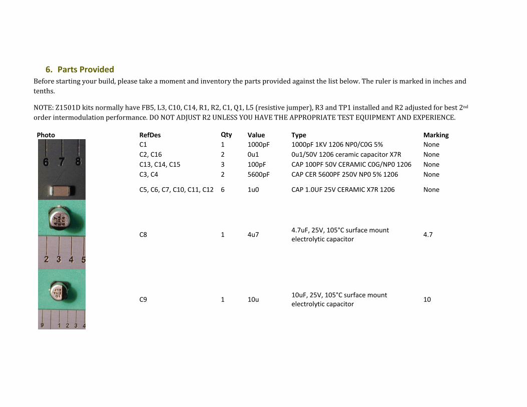
6. Parts Provided Before starting your build, please take a moment and inventory the parts provided against the list below. The ruler is marked in inches and
tenths.
NOTE: Z1501D kits normally have FB5, L3, C10, C14, R1, R2, C1, Q1, L5 (resistive jumper), R3 and TP1 installed and R2 adjusted for best 2nd
order intermodulation performance. DO NOT ADJUST R2 UNLESS YOU HAVE THE APPROPRIATE TEST EQUIPMENT AND EXPERIENCE.
Photo RefDes Qty Value Type Marking
C1 1 1000pF 1000pF 1KV 1206 NP0/C0G 5% None
C2, C16 2 0u1 0u1/50V 1206 ceramic capacitor X7R None
C13, C14, C15 3 100pF CAP 100PF 50V CERAMIC C0G/NP0 1206 None
C3, C4 2 5600pF CAP CER 5600PF 250V NP0 5% 1206 None
C5, C6, C7, C10, C11, C12 6 1u0 CAP 1.0UF 25V CERAMIC X7R 1206 None
C8 1 4u7 4.7uF, 25V, 105°C surface mount electrolytic capacitor
4.7
C9 1 10u 10uF, 25V, 105°C surface mount electrolytic capacitor
10

Z1501D Construction and Operations Manual Page 39
Photo RefDes Qty Value Type Marking
D1,D2 2 1N4148
1N4148 silicon diode, 100V 200 mA, SOD-123 outline Marking may vary with manufacturer Note: These are small parts. Do not remove from the cut tape until ready to install.
5H Or A2XN
D3 1 1N4007 Power diode, through-hole mount, 1A, 1000V.
1N4007
FB1, FB2, FB6 3 LI1812D121R-10
Ferrite bead None
FB3 1 HZ1206C20
2R-10 Ferrite bead None
FB4, FB5 2 LF1206A302R-10
Ferrite bead None
None FB7, FB8 & FB9 Ferrite beads and inductors; supplied as part of pre-assembled section of Z1501D
P1 1*
Pin header, break-apart, 6 pins total, 90 degree angle. *1 strip of 6 pins
None
Z1501D Construction and Operations Manual Page 40
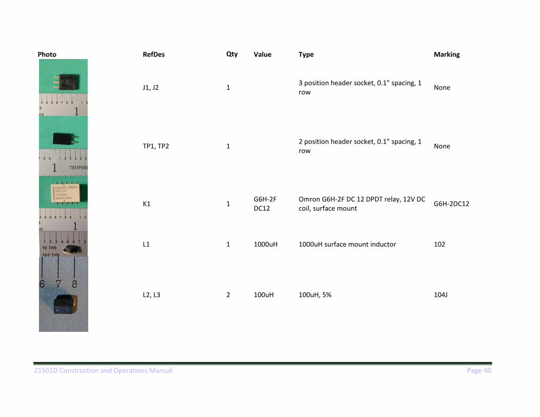
Photo RefDes Qty Value Type Marking
J1, J2 1
3 position header socket, 0.1" spacing, 1 row
None
TP1, TP2 1
2 position header socket, 0.1" spacing, 1 row
None
K1 1 G6H-2F DC12
Omron G6H-2F DC 12 DPDT relay, 12V DC coil, surface mount
G6H-2DC12
L1 1 1000uH 1000uH surface mount inductor 102
L2, L3 2 100uH 100uH, 5% 104J

Z1501D Construction and Operations Manual Page 41
Photo RefDes Qty Value Type Marking
L4 1 470uH 470uH 470U
L5 1 33 miliohms L5 is replaced with a 0.033 ohm resistor, 1812 size.
33M
Q1 1 J310
J310 N-channel JFET, TO-92 outline. Note: the J310 is static sensitive. Do not remove from the static control bag until ready to install.
J310
Q2, Q3 1 BFQ19
BFQ19, NPN transistor Note: These are small parts. Do not remove from the cut tape until ready to install.
FB
Q4 1 BFQ149
BFQ149, PNP transistor Note: These are small parts. Do not remove from the cut tape until ready to install.
FG

Z1501D Construction and Operations Manual Page 42
Photo RefDes Qty Value Type Marking
R1 1 2M21 Thick Film Resistor SMD 1/4watts 2M21 1% 1206
2214
Similar to R1 R3 1 332R Thick Film Resistor SMD 1/4watts 332R 1% 1206
3320
Similar to R1 R4, R6 2 4K70 Thick Film Resistor SMD 1/4watts 4K70 1% 1206
4701
Similar to R1 R5 1 3K3 Thick Film Resistors SMD 1/4watts 3K30 1%
3301
Similar to R1 R7 1 17R4 Thick Film Resistors SMD 1/4watts 17R4 1% 1206
17R4
R8 is not used
Similar to R1 R10 1 7K50 Thick Film Resistors SMD 1/4watts 7K50 1% 1206
7501
Similar to R1 R11 1 10K0 Thick Film Resistors SMD 1/4watts 10K0 1% 1206
1002
Similar to R1 R12 1 560R Thick Film Resistors SMD 1/4watts 560R 1% 1206
5600
R9 1 2M2
2M2 through hole resistor, ¼ watt, 5% carbon film
Red red green gold
R2 1 50K 50K, 10-turn trimmer Y503
Z1501D Construction and Operations Manual Page 43
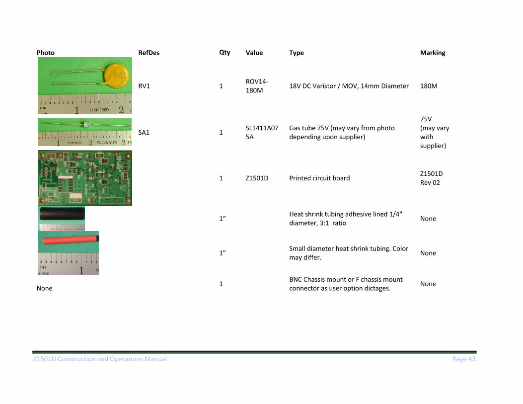
Photo RefDes Qty Value Type Marking
RV1 1 ROV14-180M
18V DC Varistor / MOV, 14mm Diameter 180M
SA1 1 SL1411A075A
Gas tube 75V (may vary from photo depending upon supplier)
75V (may vary with supplier)
1 Z1501D Printed circuit board
Z1501D Rev 02
1”
Heat shrink tubing adhesive lined 1/4" diameter, 3:1 ratio
None
1”
Small diameter heat shrink tubing. Color may differ.
None
None
1
BNC Chassis mount or F chassis mount connector as user option dictages.
None

Z1501D Construction and Operations Manual Page 44
Photo RefDes Qty Value Type Marking
Universal U-bolt & Saddle clamp set; consisting of 2 U-bolts, 2 saddle clamps and 4 nuts with integrated lock-washer.
None
L bracket, punched None
1 set
3/8-24 mobile mount ; Consists of : 3/8”x24 bolt, 3/8” split lock washer, 2 plastic shoulder washers and 1 upper threaded (3/8x24) coupler nut.
None
1
#16-22 AWG, 3/8” stud ring terminal None

Z1501D Construction and Operations Manual Page 45
Photo RefDes Qty Value Type Marking
1
Hammond 1590WBFL die cast enclosure, consisting of drilled enclosure, lid with mounting lip and gasket, 4 flat head 6-32 screws with sealing gaskets.
None
4
4-40 x 5/8" sealing pan head screw. These screws are identifiable by the red gasket material under the head.
None
4
3/16" 4-40 threaded aluminum standoffs None
8
4-40 split C lock washers; stainless steel None
4
4-40 small pattern stainless steel hex nuts None

Z1501D Construction and Operations Manual Page 46
Photo RefDes Qty Value Type Marking
1
Cable gland, consisting of retaining nut, O-ring, gland body and clamping nut
None
No photo
1 length
Approx 7 inches (175mm)
Insulated wire (center conductor from RG-58 coaxial cable)
None
4
18-8 SS Flat Head Phillips Machine Screw 6-32 Thread, 1/2" Length
None
4
6-32 Nylock stainless steel nuts None

Appendix A – Adjusting R2 for Optimum 2nd Order Intermodulation Performance
This section details two methods of adjusting the Z1501D for optimum 2nd order intermodulation
performance. The first method is a simplified approach, requiring minimal test equipment. The
second method describes how Clifton Laboratories adjusts Z1501D active antennas.
The second method is applied to assembled Z1501Ds and is also used in kit Z1501Ds. In kits, a test
fixture replicating the remainder of the Z1501D’s circuitry is plugged into the assembled input
stage and the input stage is adjusted for best 2nd order intermodulation performance. There will be
a slight difference between the settings made with the test fixture and when the kit is assembled.
This difference amounts to 2 to 3 dB and normally is not material.
Adjustment Service.
Clifton Laboratories will, without charge for the service, adjust any Z1501D kit for optimum 2nd
order intermodulation performance after it is assembled, provided:
1. The assembled Z1501D is correctly assembled.
2. The assembled Z1501D is returned to Clifton Laboratories. (The printed circuit board is all
that should be returned, not the weatherproof enclosure.)
3. A charge for return postage will be made. For US customers, $7.50 for return of the adjusted
Z1501D by Priority Mail with delivery confirmation. International customers should contact
Clifton Laboratories for the return postage price before sending the Z1501D for adjustment.
Adjustments outside the warranty period or due to mis-adjustment or incorrect assembly will incur
a service charge. Please contact Clifton Laboratories for details.
Simplified Adjustment Procedure
Theory
Traditionally 2nd order intermodulation performance is measured by applying two test tones at
frequencies f1 and f2 to the device under test. The classical 2nd order products are at frequencies
(f1-f2) and (f1+f2). It can be shown that the same mechanism is involved if f1 and f2 are identical,
so that the upper 2nd order product, f1+f2, is 2*f1. Therefore a single test tone can be applied and
the 2nd order product determined from the level of the second harmonic of the test tone. (For
quantitative measurement of 2nd order intercepts, a 3 dB adjustment should be made to the
measured second harmonic level as the single tone applies 3 dB less total power to the device under
test.) Although the simplified process removes the need for a second signal generator and
combiner, it requires the signal source and signal level measurement equipment to be free from
internal second harmonic generation. This requirement can be met by employing simple low pass
and high pass filters as described below. The filters used must be of a construction to not generate
appreciable second harmonics due to non-linearity in the inductors or capacitors.

Z1501D Construction and Operations Manual Page 48
Test Equipment Required:
1. A stable signal source, capable of an adjustable output level at 1225 KHz, with a maximum
output of at least +10 dBm.
2. Whip antenna simulator, to be constructed by the builder, requires a 49.9 ohm resistor, 15
pF C0G/NP0 capacitor and two header pins as described below.
3. A low pass filter with a cutoff frequency of 1.5 MHz and a minimum attenuation of 60 dB
(preferably more) at 2450 KHz.
4. A high pass filter with a cutoff frequency of 1.5 MHz and a minimum attenuation of 40 dB
(preferably more) at 1225 KHz.
5. Both filters should be constructed to minimize internally generated harmonics. This
requires (preferably) air core inductors or powdered iron cores. Ferrite cored inductors
will not provide acceptable results in most circumstances.
6. A 6 dB attenuator.
7. Test cable equipped with pin headers and blocking capacitor as described below.
8. A suitable device to observe the 2nd harmonic of the test source at 2450 KHz. This may be a
spectrum analyzer, a selective voltmeter or a good general coverage receiver.
9. Depending upon the device used to observe the 2nd harmonic signal level, a step attenuator
or a set of coaxial attenuators may be necessary.
10. A DC power supply, capable of supply a well regulated 13.8V at 100 mA.
DC power is normally duplexed over the Z1501D’s RF output connector, J2. For test purposes, it is
more convenient to employ a separate DC power supply connected with clip leads between RV1’s
positive lead and ground. (RV1 is the over-voltage MOV.)
At Clifton Laboratories, an HP E3601A variable voltage power supply is used for this purpose.
Z1501D Construction and Operations Manual Page 49
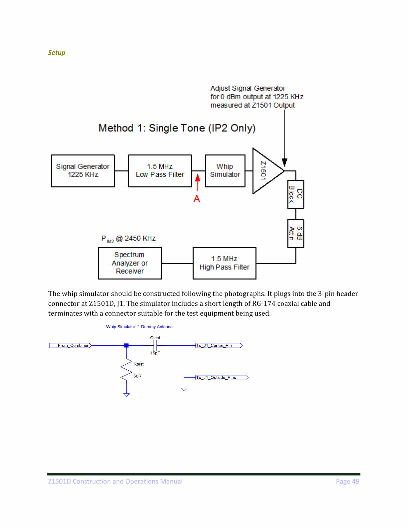
Setup
The whip simulator should be constructed following the photographs. It plugs into the 3-pin header
connector at Z1501D, J1. The simulator includes a short length of RG-174 coaxial cable and
terminates with a connector suitable for the test equipment being used.
Z1501D Construction and Operations Manual Page 50
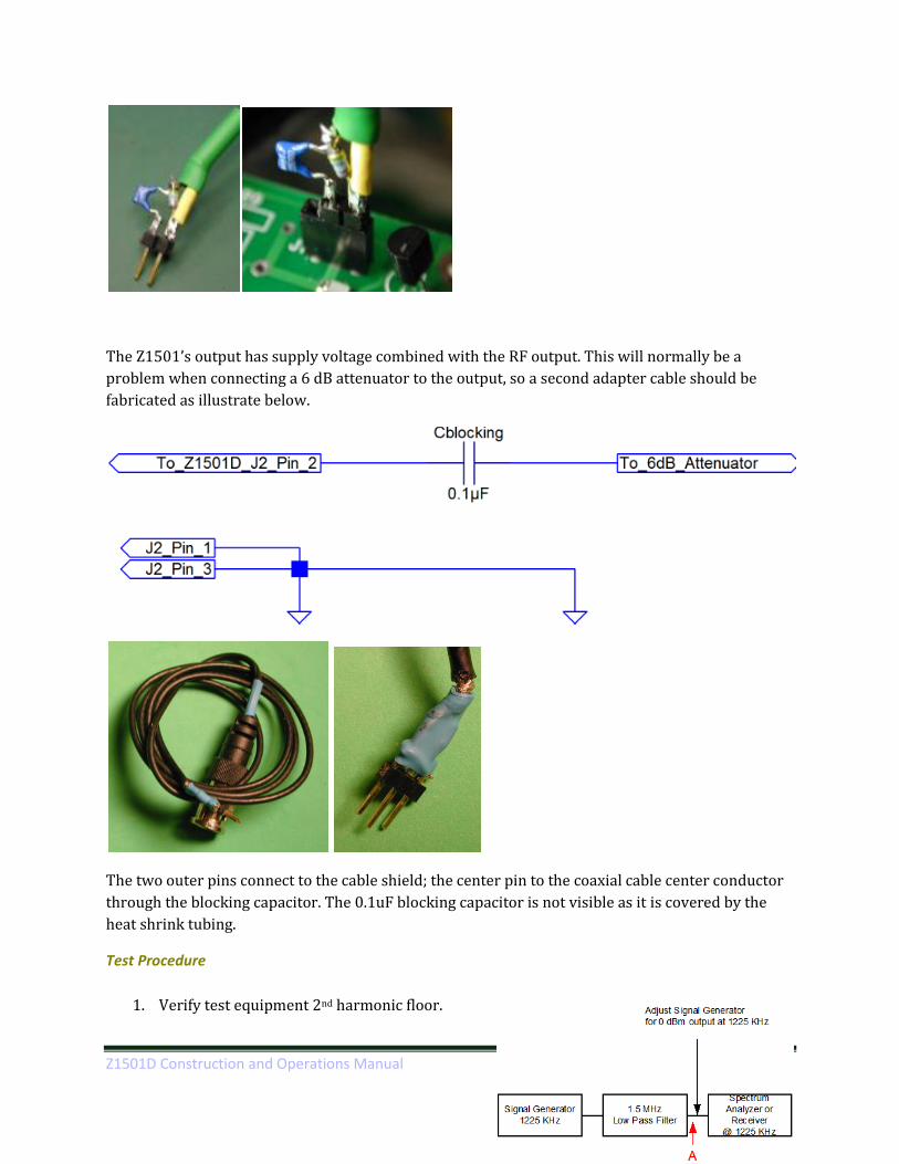
The Z1501’s output has supply voltage combined with the RF output. This will normally be a
problem when connecting a 6 dB attenuator to the output, so a second adapter cable should be
fabricated as illustrate below.
The two outer pins connect to the cable shield; the center pin to the coaxial cable center conductor
through the blocking capacitor. The 0.1uF blocking capacitor is not visible as it is covered by the
heat shrink tubing.
Test Procedure
1. Verify test equipment 2nd harmonic floor.

Z1501D Construction and Operations Manual Page 51
a. Temporarily connect the signal level measuring equipment to the 1.5 MHz low pass
filter output, as shown at the right. (Point A in the setup drawing.)
b. Set the signal generator to 1225 KHz and adjust the signal generator output level to
result in a 0.0 dBm output level at the 1.5 MHz low pass filter output.
c. Connect the 1.5 MHz low pass filter output to the 1.5 MHz high pass filter input.
Connect the signal measuring device to
the 1.5 MHz high pass filter output as
shown at the setup drawing at the right.
Set the signal measuring device to the
2450 KHz and observe the signal level. If
the 2450 KHz signal level exceeds -100
dBm, you are likely to have difficulty
completing the rest of the measurements.
2. Adjust level at Z1501D output
a. Temporarily connect the Z1501D’s output, using the adapter cable, to the signal
level measuring equipment as illustrated in the figure below right.
b. Set the signal level measuring device to 1225 KHz.
c. Connect the low pass filter
output to the Z1501D using the
whip simulation circuit.
d. Set the signal generator to 1225
KHz and adjust the signal
generator output level to result
in a 0.0 dBm output level from
the Z1501D.
3. Measure 2nd Harmonic Level Through
Z1501D and Adjust R2
a. Configure the equipment as
shown in the Setup illustration,
reproduced below, with the
Z1501D’s output connected to
the 6 dB attenuator and the signal measuring device to the 1.5 MHz high pass filter.
b. Leaving the signal generator at 1225 KHz, and without changing the signal
generator level, adjust the
measuring device to the second
harmonic frequency, i.e., 2450
KHz.
c. Adjust R2 for minimum signal
level at 2450 KHz.

Z1501D Construction and Operations Manual Page 52
d. The observed 2450 KHz signal level should not exceed -88 dBm. This corresponds to
an actual signal level of approximately -80 dBm out of the Z1501D, adjusted for the
6 dB attenuator and 1.5 MHz high pass filter loss.
Full Performance Verification
If the appropriate test equipment is available, a full 2nd and 3rd order intermodulation performance
measurement may be made, with the bias potentiometer, R2, being adjusted as part of the
performance verification.
Since it is unlikely that the exact equipment used at Clifton Laboratories will be found in other
shops, the setup below should be regarded as advisory and may be altered as appropriate to match
the equipment available.
Note that the Z1501D has high 2nd and 3rd order intercepts and that care must be taken to avoid test
equipment induced intermodulation artifacts.
Setup
HP 8657A
Signal Generator
3007 KHz
6 MHz
Low Pass Filter
Z1501HP 8568B
Spectrum
Analyzer
2nd and 3rd Order Intermodulation Protocol for Z1501D Active Antenna
HP 8657A
Signal Generator
4011KHz
3 MHz
Low Pass Filter
Mini-Circuits
ZFSC-2-6+
Combiner
6 dB
Att'n
OIP2 = 2*Po - *PIM2
*PIM2
= measured power of 2nd order
intermodulation products
PO = test tone output power
*PIM3
= measured power of 3rd order
intermodulation products.
PO = test tone output power
OIP3 = 1/2*(3*Po - *PIM3
)
All power measured in dBm
ZH
L-3
AZ
HL-3
A
6 dB
Att'n
6 dB
Att'n
6 dB
Att'n
Whip
Simulator
Adjust signal generator output for 0
dBm per tone at Z1501D output
HP E3610
DC Power Supply
to Z1501

Z1501D Construction and Operations Manual Page 53
Test Procedure Overview
Configure test equipment as in the block diagram.
1. Adjust the Z1501D’s supply voltage to 13.80 volts. (DC power is normally duplexed over the
Z1501D’s RF output connector, J2. For test purposes, it is more convenient to employ a
separate DC power supply connected with clip leads between RV1’s positive lead and
ground. (RV1 is the over-voltage MOV.) At Clifton Laboratories, an HP E3601A variable
voltage power supply is used for this purpose.)
2. Allow warm up time and execute HP 8568B self-calibration routines.
3. Adjust HP 8567A signal generators to produce 0.0 dBm output from the amplifier under test
at the two test tones, normally 3007 and 4011 KHz.
4. Set the 8568B for 10 Hz RBW, 10 Hz VBW, Span 200 Hz, video (trace) average = 16, and
center frequency corresponding to the intermodulation product being measured. Set
attenuation to 50 dB for 2nd order products and 40 dB for 3rd order products. If the Z1501’s
bias potentiometer has already been set, record the peak level.
5. If not, before collecting data, adjust the Z1501 bias potentiometer (R2) for minimum 2nd
order intermodulation product at 1004 KHz. Adjusting the bias potentiometer under this
condition has proven to provide good 2nd order intermodulation performance across the
medium wave and shortwave bands.
6. The strategy of adjusting at the frequency of worst 2nd order performance, 7018 KHz in the
Z1501D, is not recommended as the optimum bias setting cannot be easily found due to the
small change in intermodulation product level with changes in bias voltage.
7. Intermodulation frequencies to be observed:
a. 2nd order: 1004 KHz
b. 3rd order 2003 KHz
c. 3rd order 5015 KHz
d. 2nd order 7018 KHz
8. The reason for the “odd” tone frequencies instead of 3000.000 KHz and 4000.000 KHz are
to prevent discrete synthesizer spurious signals from the HP 8657A signal generators from
landing on top of the intermodulation product frequency being measured. Other generators,
such as the HP 8640B, do not have this problem and may be used with 3.000 and 4.000 MHz
test tones.
9. More broadly, why frequencies near 3 and 4 MHz? These are typical test frequencies used
with the World Radio and Television Handbook tests of active antennas a few years ago.
Frequencies in this range allow good mid-range HF IMD testing for 3rd order products and
into the medium wave band for 2nd order.
10. Test tones in the medium wave band at 603 and 707 KHz are also used at Clifton
Laboratories in measuring the Z1501D’s intermodulation performance.
11. Performance levels observed will be:
a. 1004 KHz: minimum: -80 dBm, typically less than -88 dBm
b. 2003 KHz & 5015 KHz: typically -80 to -82 dBm
c. 7018 KHz: typically -72 to -74 dBm.

Z1501D Construction and Operations Manual Page 54
Appendix B – Typical Phase Shift amongst Multiple Z1501D and Z1203A Units One use of the Z1501D and Z1203A couplers is in a phase array. At the simplest, two Z1501D’s may
be used to null unwanted signals or provide gain in a particular direction through a “phaser” or
combining mechanism with amplitude and phase adjustment. This concept may be extended to four
or more Z1501D active antennas, such as in a “four square” array.
When used in a phased array, it is desirable for all active antennas to exhibit similar phase shift, i.e.,
their differential phase should be close to zero. The absolute phase is not of significance so long as
all antennas have the same absolute phase. Thus, in the plots below the critical factor to observe is
not that the antennas have phase shift but rather how closely the phase shift of the antennas match.
In the ideal situation, the phase plots would all fall on top of each other, indicating perfect phase
matching. The degree to which the phase plots diverge from each other is a measure of differential
phase error.
In addition to phase, it is desirable that the antennas have matched amplitude response as well.
To assess the differential phase response of the Z1501D active antenna and Z1203A coupler, a
sample of four production Z1501D active antennas and two Z1203A couplers were compared in
amplitude and phase response using an HP 87510A vector network analyzer, over the range 1 KHz
to 100 MHz.
In all cases, the active antenna is connected to the vector network analyzer through the whip
simulator circuit described in Appendix A.
The test fixture connection does not use an external coupler, but rather directly connects the
Z1501D’s output to the 87510A VNA. DC power is supplied to the Z1501D with clip leads connected
across RV1, the over-voltage MOV. The purpose of this measurement is to determine the relative
amplitude and phase response of the Z1501D standing alone, without a DC power coupler. (The
Z1501D is easily modifiable so that power may be supplied independently of the coaxial feedline,
should this be desirable.)

Z1501D Construction and Operations Manual Page 55
Amplitude Match – Z1501D Alone
The plot below compares the amplitude response of four Z1501D active antennas without coupler.
The amplitude responses are, for all practical purposes, identical over the full rated frequency
range of 20 KHz to 30 MHz. (Note all plots employ a log frequency axis.)
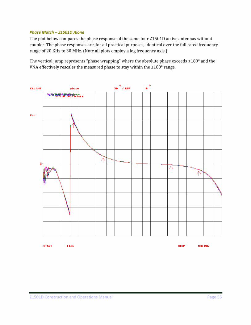
Z1501D Construction and Operations Manual Page 56
Phase Match – Z1501D Alone
The plot below compares the phase response of the same four Z1501D active antennas without
coupler. The phase responses are, for all practical purposes, identical over the full rated frequency
range of 20 KHz to 30 MHz. (Note all plots employ a log frequency axis.)
The vertical jump represents “phase wrapping” where the absolute phase exceeds ±180° and the
VNA effectively rescales the measured phase to stay within the ±180° range.
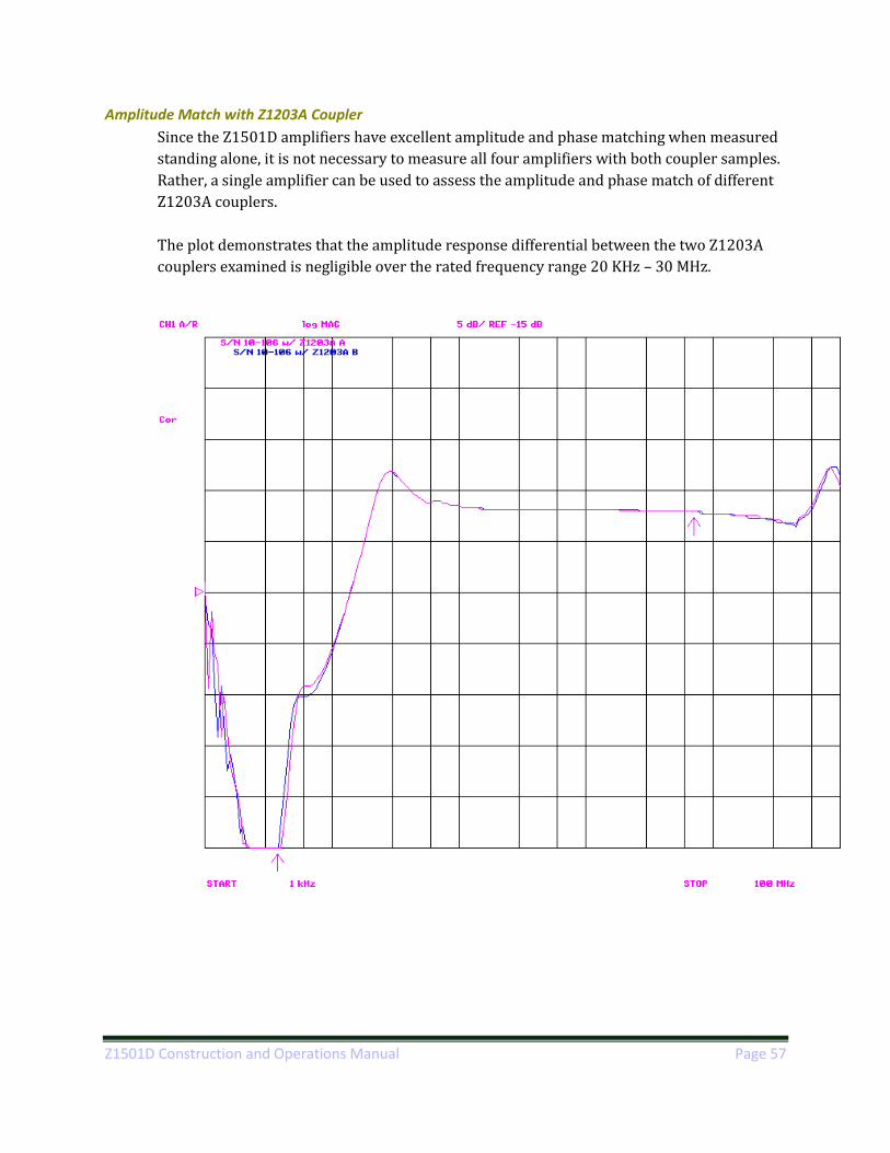
Z1501D Construction and Operations Manual Page 57
Amplitude Match with Z1203A Coupler
Since the Z1501D amplifiers have excellent amplitude and phase matching when measured
standing alone, it is not necessary to measure all four amplifiers with both coupler samples.
Rather, a single amplifier can be used to assess the amplitude and phase match of different
Z1203A couplers.
The plot demonstrates that the amplitude response differential between the two Z1203A
couplers examined is negligible over the rated frequency range 20 KHz – 30 MHz.

Z1501D Construction and Operations Manual Page 58
Phase Match with Z1203A Coupler
Since the Z1501D amplifiers have excellent amplitude and phase matching when measured
standing alone, it is not necessary to measure all four amplifiers with both coupler samples.
Rather, a single amplifier can be use to assess the amplitude and phase match of different
Z1203A couplers.
The plot demonstrates that the phase response differential between the two Z1203A
couplers examined is negligible over the rated frequency range 20 KHz – 30 MHz.