xx antenna, schematic, layout and esign …eecs.oregonstate.edu/~traylor/ece473/pdfs/an383.pdf ·...
TRANSCRIPT
Rev. 0.4 6/08 Copyright © 2008 by Silicon Laboratories AN383
AN383
Si47XX ANTENNA, SCHEMATIC, LAYOUT, AND DESIGN GUIDELINES
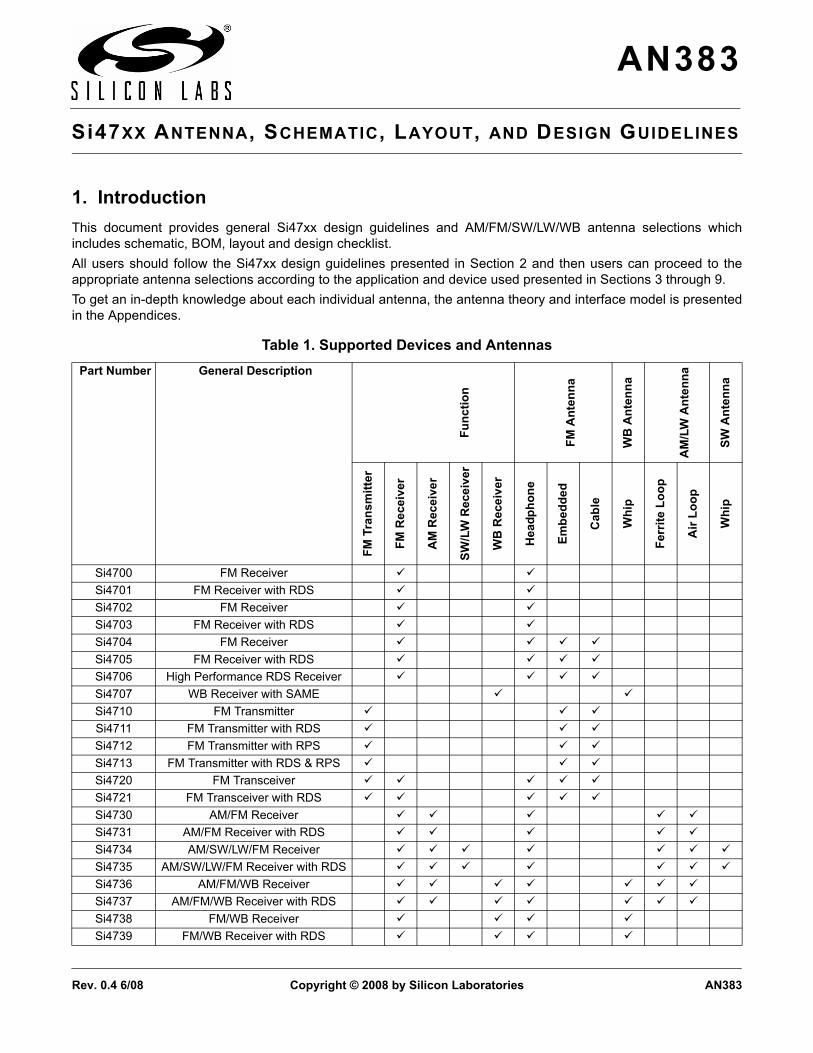
1. IntroductionThis document provides general Si47xx design guidelines and AM/FM/SW/LW/WB antenna selections whichincludes schematic, BOM, layout and design checklist.All users should follow the Si47xx design guidelines presented in Section 2 and then users can proceed to theappropriate antenna selections according to the application and device used presented in Sections 3 through 9.To get an in-depth knowledge about each individual antenna, the antenna theory and interface model is presentedin the Appendices.
Table 1. Supported Devices and Antennas Part Number General Description
Func
tion
FM A
nten
na
WB
Ant
enna
AM
/LW
Ant
enna
SW A
nten
na
FM T
rans
mitt
er
FM R
ecei
ver
AM
Rec
eive
r
SW/L
W R
ecei
ver
WB
Rec
eive
r
Hea
dpho
ne
Embe
dded
Cab
le
Whi
p
Ferr
ite L
oop
Air
Loop
Whi
p
Si4700 FM Receiver Si4701 FM Receiver with RDS Si4702 FM Receiver Si4703 FM Receiver with RDS Si4704 FM Receiver Si4705 FM Receiver with RDS Si4706 High Performance RDS Receiver Si4707 WB Receiver with SAME Si4710 FM Transmitter Si4711 FM Transmitter with RDS Si4712 FM Transmitter with RPS Si4713 FM Transmitter with RDS & RPS Si4720 FM Transceiver Si4721 FM Transceiver with RDS Si4730 AM/FM Receiver Si4731 AM/FM Receiver with RDS Si4734 AM/SW/LW/FM Receiver Si4735 AM/SW/LW/FM Receiver with RDS Si4736 AM/FM/WB Receiver Si4737 AM/FM/WB Receiver with RDS Si4738 FM/WB Receiver Si4739 FM/WB Receiver with RDS
AN383
2 Rev. 0.4
AN383
Rev. 0.4 3
TABLE OF CONTENTS
Section Page1. Introduction . . . . . . . . . . . . . . . . . . . . . . . . . . . . . . . . . . . . . . . . . . . . . . . . . . . . . . . . . . . . .12. Si47xx 3x3 mm QFN Schematic and Layout . . . . . . . . . . . . . . . . . . . . . . . . . . . . . . . . . . .5
2.1. Si47xx 3x3 mm Design . . . . . . . . . . . . . . . . . . . . . . . . . . . . . . . . . . . . . . . . . . . . . . . .52.2. Si47xx 3x3 mm Schematic . . . . . . . . . . . . . . . . . . . . . . . . . . . . . . . . . . . . . . . . . . . . .72.3. Si47xx 3x3 mm Bill of Materials . . . . . . . . . . . . . . . . . . . . . . . . . . . . . . . . . . . . . . . . .82.4. Si47xx 3x3 mm Layout . . . . . . . . . . . . . . . . . . . . . . . . . . . . . . . . . . . . . . . . . . . . . . . .92.5. Si47xx 3x3 mm Design Checklist . . . . . . . . . . . . . . . . . . . . . . . . . . . . . . . . . . . . . . .13
3. Headphone Antenna for FM Receive (Si470x/2x/3x Only) . . . . . . . . . . . . . . . . . . . . . . .143.1. Headphone Antenna Design . . . . . . . . . . . . . . . . . . . . . . . . . . . . . . . . . . . . . . . . . . .143.2. Headphone Antenna Schematic . . . . . . . . . . . . . . . . . . . . . . . . . . . . . . . . . . . . . . . .153.3. Headphone Antenna Bill of Materials . . . . . . . . . . . . . . . . . . . . . . . . . . . . . . . . . . . .163.4. Headphone Antenna Layout . . . . . . . . . . . . . . . . . . . . . . . . . . . . . . . . . . . . . . . . . . .173.5. Headphone Antenna Design Checklist . . . . . . . . . . . . . . . . . . . . . . . . . . . . . . . . . . .17
4. Embedded Antenna for FM Transmit and Receive (Si4704/05/06/1x/2x Only) . . . . . . .184.1. Embedded Antenna Design . . . . . . . . . . . . . . . . . . . . . . . . . . . . . . . . . . . . . . . . . . .184.2. Embedded Antenna Schematic . . . . . . . . . . . . . . . . . . . . . . . . . . . . . . . . . . . . . . . . .244.3. Embedded Antenna Bill of Materials . . . . . . . . . . . . . . . . . . . . . . . . . . . . . . . . . . . . .254.4. Embedded Antenna Layout . . . . . . . . . . . . . . . . . . . . . . . . . . . . . . . . . . . . . . . . . . . .254.5. Embedded Antenna Design Checklist . . . . . . . . . . . . . . . . . . . . . . . . . . . . . . . . . . . .26
5. Cable Antenna for FM Transmit and Receive (Si4704/05/06/1x/2x Only) . . . . . . . . . . .275.1. Cable Antenna Design . . . . . . . . . . . . . . . . . . . . . . . . . . . . . . . . . . . . . . . . . . . . . . .275.2. Cable Antenna Schematic . . . . . . . . . . . . . . . . . . . . . . . . . . . . . . . . . . . . . . . . . . . . .275.3. Cable Antenna Bill of Materials . . . . . . . . . . . . . . . . . . . . . . . . . . . . . . . . . . . . . . . . .285.4. Cable Antenna Layout . . . . . . . . . . . . . . . . . . . . . . . . . . . . . . . . . . . . . . . . . . . . . . . .295.5. Cable Antenna Design Checklist . . . . . . . . . . . . . . . . . . . . . . . . . . . . . . . . . . . . . . . .29
6. Whip Antenna for FM/WB Receiver (Si4736/37/38/39 Only) . . . . . . . . . . . . . . . . . . . . . .306.1. FM/WB Whip Antenna Design . . . . . . . . . . . . . . . . . . . . . . . . . . . . . . . . . . . . . . . . .306.2. FM/WB Whip Antenna Schematic . . . . . . . . . . . . . . . . . . . . . . . . . . . . . . . . . . . . . . .306.3. FM/WB Whip Antenna Bill of Materials . . . . . . . . . . . . . . . . . . . . . . . . . . . . . . . . . .316.4. FM/WB Whip Antenna Layout . . . . . . . . . . . . . . . . . . . . . . . . . . . . . . . . . . . . . . . . . .316.5. FM/WB Whip Antenna Design Checklist . . . . . . . . . . . . . . . . . . . . . . . . . . . . . . . . .31
7. Ferrite Loop Antenna for AM/LW Receive (Si4730/31/34/35/36/37 Only) . . . . . . . . . . . .327.1. Ferrite Loop Antenna Design . . . . . . . . . . . . . . . . . . . . . . . . . . . . . . . . . . . . . . . . . .327.2. Ferrite Loop Antenna Schematic . . . . . . . . . . . . . . . . . . . . . . . . . . . . . . . . . . . . . . . .337.3. Ferrite Loop Antenna Bill of Materials . . . . . . . . . . . . . . . . . . . . . . . . . . . . . . . . . . . .337.4. Ferrite Loop Antenna Layout . . . . . . . . . . . . . . . . . . . . . . . . . . . . . . . . . . . . . . . . . . .337.5. Ferrite Loop Antenna Design Checklist . . . . . . . . . . . . . . . . . . . . . . . . . . . . . . . . . . .34
8. Air Loop Antenna for AM/LW Receive (Si4730/31/34/35/36/37 Only) . . . . . . . . . . . . . . .358.1. Air Loop Antenna Design . . . . . . . . . . . . . . . . . . . . . . . . . . . . . . . . . . . . . . . . . . . . .358.2. Air Loop Antenna Schematic . . . . . . . . . . . . . . . . . . . . . . . . . . . . . . . . . . . . . . . . . . .368.3. Air Loop Antenna Bill of Materials . . . . . . . . . . . . . . . . . . . . . . . . . . . . . . . . . . . . . . .36
AN383
4 Rev. 0.4
8.4. Air Loop Antenna Layout . . . . . . . . . . . . . . . . . . . . . . . . . . . . . . . . . . . . . . . . . . . . . .378.5. Air Loop Antenna Design Checklist . . . . . . . . . . . . . . . . . . . . . . . . . . . . . . . . . . . . . .37
9. Whip Antenna for SW Receiver (Si4734/35 Only) . . . . . . . . . . . . . . . . . . . . . . . . . . . . . .389.1. SW Whip Antenna Design . . . . . . . . . . . . . . . . . . . . . . . . . . . . . . . . . . . . . . . . . . . . .389.2. SW Whip Antenna Schematic . . . . . . . . . . . . . . . . . . . . . . . . . . . . . . . . . . . . . . . . . .399.3. SW Whip Antenna Bill of Materials . . . . . . . . . . . . . . . . . . . . . . . . . . . . . . . . . . . . . .419.4. SW Whip Antenna Layout . . . . . . . . . . . . . . . . . . . . . . . . . . . . . . . . . . . . . . . . . . . . .419.5. SW Whip Antenna Design Checklist . . . . . . . . . . . . . . . . . . . . . . . . . . . . . . . . . . . . .41
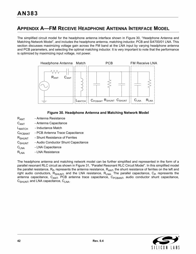
Appendix A—FM Receive Headphone Antenna Interface Model . . . . . . . . . . . . . . . . . . . .42Appendix B—FM Transmit Embedded Antenna Interface Model . . . . . . . . . . . . . . . . . . .47Appendix C—AM Ferrite Loop Stick Antenna Interface Model . . . . . . . . . . . . . . . . . . . . .54Document Change List . . . . . . . . . . . . . . . . . . . . . . . . . . . . . . . . . . . . . . . . . . . . . . . . . . . . .58Contact Information . . . . . . . . . . . . . . . . . . . . . . . . . . . . . . . . . . . . . . . . . . . . . . . . . . . . . . . .60

AN383
Rev. 0.4 5
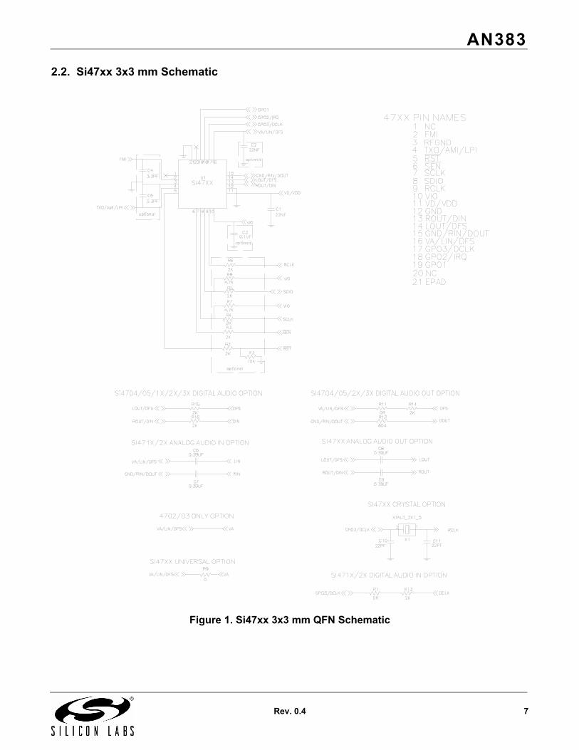
2. Si47xx 3x3 mm QFN Schematic and LayoutThis section shows the minimal schematic and layout options required for optimal Si47xx performance. Populationoptions are provided to support the layout for all 3 x 3 mm QFN devices, mitigate system noise, operate theinternal oscillator with external crystal, and filter VCO energy.
2.1. Si47xx 3x3 mm DesignC1 (22 nF) is a required bypass capacitor for VD/VDD supply pin 11. Place C1 as close as possible to the VD/VDDpin 11 and GND pin 12. Place a VIA connecting C1 VD/VDD supply to the power rail such that the cap is closer tothe Si47xx than the VIA. Route C1 GND directly and only to GND pin 12 with a wide, low inductance trace. Theserecommendations are made to reduce the size of the current loop created by the bypass cap and routing, minimizebypass cap impedance and return all currents to the GND pad.C2 (22 nF) is an optional bypass capacitor for VA/LIN/DFS supply pin 16 (Si4702/03 only) and may be placed tomitigate supply noise. Place C2 as close as possible to the VA/LIN/DFS pin 16 and GND pin 15. Place a VIAconnecting C2 VA supply to the power rail such that the cap is closer to the Si47xx than the VIA. Route C2 GNDdirectly and only to GND pin 15 with a wide, low inductance trace. Route GND/RIN/DOUT pin 15 to the GND pad ifdesigning only for the Si4702/03. If designing for all Si47xx devices, do not route GND/RIN/DOUT pin 15 to theGND pad. In this case the on-chip connection between pin 15 and the GND pad will provide a ground connection.These recommendations are made to reduce the size of the current loop created by the bypass cap and routing,minimize bypass cap impedance and return all currents to the GND pad.C3 (100 nF) is an optional bypass capacitor for the VIO supply pin 10 and may be placed to mitigate supply noise.Place C3 as close as possible to the VIO pin 10 and the GND pin 12. Place a VIA connecting C3 VIO supply to thepower rail such that the cap is closer to the Si47xx than the VIA. Route C3 GND directly and only to GND pin 12with a wide, low inductance trace. These recommendations are made to reduce the size of the current loop createdby the bypass cap and routing, minimize bypass cap impedance and return all currents to the GND pad.C4 (2–5 pF) is an optional filter capacitor for FMI pin 2 and may be placed to shunt VCO energy to GND andprevent it from radiating from an antenna connected to the FMI pin. This filter is only required if regulatory testingrequires measuring emissions at the VCO frequency of 3 to 4 GHz and the antenna implementation is an efficientradiator at these frequencies. Place C4 as close as possible to FMI pin 2 and RFGND pin 3. Place a VIAconnecting C4 FMI to another layer as needed such that the cap is closer to the Si47xx than the VIA. Route FMIpin 2 to GND if the pin functionality is not used.C5 (2–5 pF) is an optional filter capacitor for TXO/AMI/LPI pin 4 and may be placed to shunt VCO energy to GNDand prevent it from radiating from an antenna connected to the TXO/AMI/LPI pin. The guidelines for C5 areidentical to those for C4. Route TXO/AMI/LPI pin 4 to GND if the pin functionality is not used.C6 and C7 (0.39µF) are ac coupling caps for transmitter audio input to VA/LIN/DFS pin 16 and GND/DIN/DOUT pin15 (Si471x/2x analog audio input mode only). The input resistance of the transmitter audio input and the cap willset the high pass pole given by Equation 1. The input resistance of the audio input is programmatically selectableas 396 kΩ, 100 kΩ, 74 kΩ, or 60 kΩ (default). Placement location is not critical.
Equation 1. High-Pass Pole CalculationC8 and C9 (0.39 µF) are ac coupling caps for receiver analog audio output from ROUT/DIN pin 14 and LOUT/DFSpin 15 (Si4702/03/04/05/2x/3x audio output mode only). The input resistance of the amplifier, such as a headphoneamplifier, and the capacitor will set the high pass pole given by Equation 1. Placement location is not critical.C10 and C11 (7–22 pF) are optional crystal loading caps required only when using the internal oscillator feature.Refer to the crystal data sheet for the proper load capacitance and be certain to account for parasitic capacitance.Place caps C10 and C11 such that they share a common GND connection and the current loop area of the crystaland loading caps is minimized.
fc1
2πRC----------------=
AN383
6 Rev. 0.4
X1 (32.768 kHz) is an optional crystal required only when using the internal oscillator feature. Place the crystal X1as close to GPO3/DCLK pin 17 and RCLK pin 9 as possible to minimize current loops. Route the RCLK trace as farfrom SDIO pin 8 and SDIO trace as possible to minimize capacitive coupling.R1 (0 Ω) is an optional jumper used to route the digital audio clock to GPO3/DCLK pin 17. R1 is only required for adesign in which the crystal and digital audio (Si4704/05/1x/2x/3x only) BOM options are desired. Populate R1 andremove C10, C11 and X1 when using digital audio. Populate C10, C11, and X1 and remove R1 when using theinternal oscillator. Place resistor R1 as close to DCLK/GPO3 pin 17 as possible as shown in Layout Example 4 tominimize trace length from pin 17 to the crystal and load cap.R2-R6 (25 Ω–2 kΩ) are optional series termination resistors and are used to mitigate system noise. Therecommended value of the resistors is 2 kΩ for optimal edge rate and noise suppression. Confirm that timingrequirements are met with the selected series termination resistor value. Place the series termination resistors R2-R6 as close to the host controller as possible.R7 and R8 (4.7 kΩ) are optional pull-up resistors for the SCLK and SDIO lines required only when using an I2Cbus. The size of pull-up resistor value will vary based on the number of devices, capacitance and speed of the bus.Placement location is not critical. Refer to the I2C specification for additional design information. R9 (0 Ω) is used to route power to VA/LIN/DFS supply pin 16. R9 is only required to support a layout for all 3x3 mmQFN devices. If designing for the Si4702/03 only R9 may be replaced with trace connections. If designing forSi4704/05/1x/2x/3x only, R9 is not required. Place resistor R9 as close to VA/LIN/DFS pin 16 as possible. R11 (0 Ω) is an optional jumper used to route the DFS to VA/LIN/DFS pin 16. R11 is only required for a design inwhich the Si4702/03 and digital audio output (Si4704/05/2x/3x) BOM options are desired. Place resistor R11 asclose to pin VA/LIN/DFS 16 as possible.R12 (25 Ω–2 kΩ) is a required series termination resistor when using digital audio output (Si4704/05/2x/3x only)and is used to mitigate noise from the digital data routed from GND/RIN/DOUT pin 15. The recommended value ofthe resistor is 604 Ω for optimal edge rate and noise suppression. Confirm that timing requirements are met withthe selected series termination resistor value. Place R12 as close to pin 15 as possible.R13 (25 Ω–2 kΩ) is a required series termination resistor when using digital audio (Si4704/05/1x/2x/3x only) and isused to mitigate noise from the digital clock routed to GPO3/DCLK pin 17. The recommended value of the resistoris 2 kΩ for optimal edge rate and noise suppression. Confirm that timing requirements are met with the selectedseries termination resistor value. Place R13 as close to the host controller as possible.R14 (25 Ω–2 kΩ) is a required series termination resistor when using digital audio output (Si4704/05/2x/3x only)and is used to mitigate noise from the digital frame clock routed to VA/LIN/DFS pin 16. The recommended value ofthe resistor is 2 kΩ for optimal edge rate and noise suppression. Confirm that timing requirements are met with theselected series termination resistor value. Place R14 as close to the host controller as possible.R15 (25 Ω–2 kΩ) is a required series termination resistor when using digital audio input (Si471x/2x only) and isused to mitigate noise from the digital frame clock routed to LOUT/DFS pin 14. The recommended value of theresistor is 2 kΩ for optimal edge rate and noise suppression. Confirm that timing requirements are met with theselected series termination resistor value. Place R15 as close to the host controller as possible.R16 (25 Ω–2 kΩ) is a required series termination resistor when using digital audio input (Si471x/2x only) and isused to mitigate noise from the digital data routed to ROUT/DIN pin 13. The recommended value of the resistors is2 kΩ for optimal edge rate and noise suppression. Confirm that timing requirements are met with the selectedseries termination resistor value. Place R16 as close to the host controller as possible.
AN383
Rev. 0.4 7
2.2. Si47xx 3x3 mm Schematic
Figure 1. Si47xx 3x3 mm QFN Schematic
AN383
8 Rev. 0.4
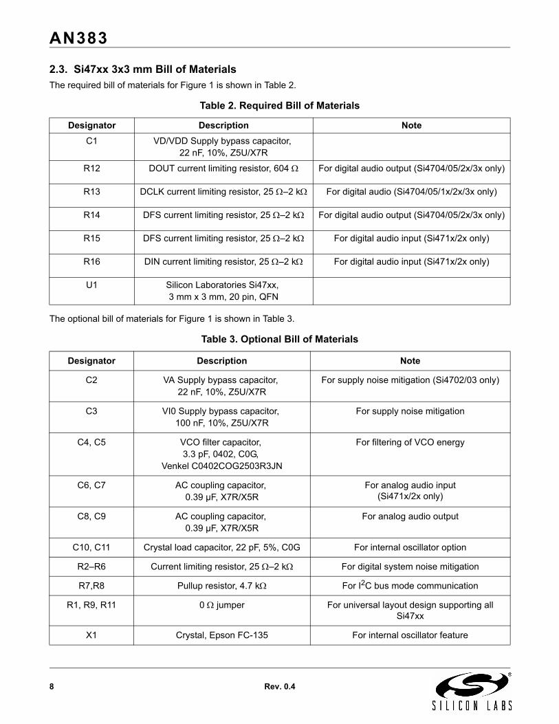
2.3. Si47xx 3x3 mm Bill of MaterialsThe required bill of materials for Figure 1 is shown in Table 2.
The optional bill of materials for Figure 1 is shown in Table 3.
Table 2. Required Bill of Materials
Designator Description NoteC1 VD/VDD Supply bypass capacitor,
22 nF, 10%, Z5U/X7R
R12 DOUT current limiting resistor, 604 Ω For digital audio output (Si4704/05/2x/3x only)
R13 DCLK current limiting resistor, 25 Ω–2 kΩ For digital audio (Si4704/05/1x/2x/3x only)
R14 DFS current limiting resistor, 25 Ω–2 kΩ For digital audio output (Si4704/05/2x/3x only)
R15 DFS current limiting resistor, 25 Ω–2 kΩ For digital audio input (Si471x/2x only)
R16 DIN current limiting resistor, 25 Ω–2 kΩ For digital audio input (Si471x/2x only)
U1 Silicon Laboratories Si47xx, 3 mm x 3 mm, 20 pin, QFN
Table 3. Optional Bill of Materials
Designator Description Note
C2 VA Supply bypass capacitor, 22 nF, 10%, Z5U/X7R
For supply noise mitigation (Si4702/03 only)
C3 VI0 Supply bypass capacitor, 100 nF, 10%, Z5U/X7R
For supply noise mitigation
C4, C5 VCO filter capacitor, 3.3 pF, 0402, C0G,
Venkel C0402COG2503R3JN
For filtering of VCO energy
C6, C7 AC coupling capacitor, 0.39 µF, X7R/X5R
For analog audio input(Si471x/2x only)
C8, C9 AC coupling capacitor, 0.39 µF, X7R/X5R
For analog audio output
C10, C11 Crystal load capacitor, 22 pF, 5%, C0G For internal oscillator option
R2–R6 Current limiting resistor, 25 Ω–2 kΩ For digital system noise mitigation
R7,R8 Pullup resistor, 4.7 kΩ For I2C bus mode communication
R1, R9, R11 0 Ω jumper For universal layout design supporting all Si47xx
X1 Crystal, Epson FC-135 For internal oscillator feature
AN383
Rev. 0.4 9
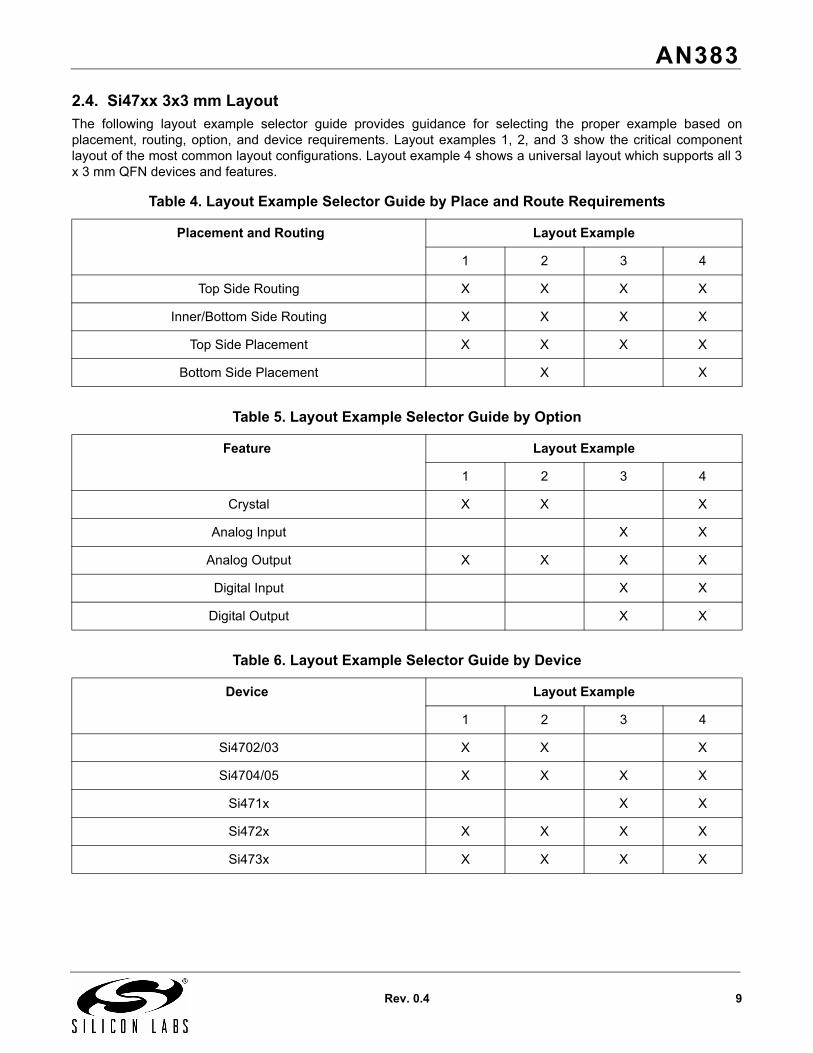
2.4. Si47xx 3x3 mm LayoutThe following layout example selector guide provides guidance for selecting the proper example based onplacement, routing, option, and device requirements. Layout examples 1, 2, and 3 show the critical componentlayout of the most common layout configurations. Layout example 4 shows a universal layout which supports all 3x 3 mm QFN devices and features.
Table 4. Layout Example Selector Guide by Place and Route Requirements
Placement and Routing Layout Example
1 2 3 4
Top Side Routing X X X X
Inner/Bottom Side Routing X X X X
Top Side Placement X X X X
Bottom Side Placement X X
Table 5. Layout Example Selector Guide by Option
Feature Layout Example
1 2 3 4
Crystal X X X
Analog Input X X
Analog Output X X X X
Digital Input X X
Digital Output X X
Table 6. Layout Example Selector Guide by Device
Device Layout Example
1 2 3 4
Si4702/03 X X X
Si4704/05 X X X X
Si471x X X
Si472x X X X X
Si473x X X X X
AN383
10 Rev. 0.4
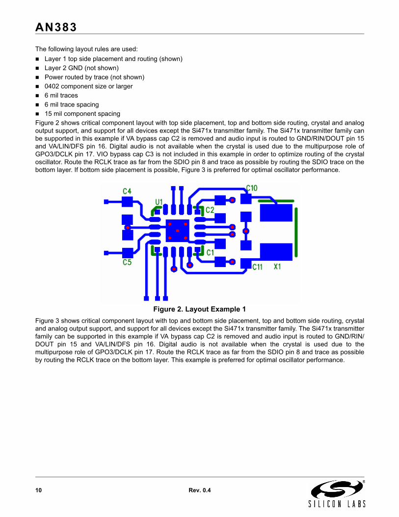
The following layout rules are used:Layer 1 top side placement and routing (shown)Layer 2 GND (not shown)Power routed by trace (not shown)0402 component size or larger6 mil traces6 mil trace spacing15 mil component spacing
Figure 2 shows critical component layout with top side placement, top and bottom side routing, crystal and analogoutput support, and support for all devices except the Si471x transmitter family. The Si471x transmitter family canbe supported in this example if VA bypass cap C2 is removed and audio input is routed to GND/RIN/DOUT pin 15and VA/LIN/DFS pin 16. Digital audio is not available when the crystal is used due to the multipurpose role ofGPO3/DCLK pin 17. VIO bypass cap C3 is not included in this example in order to optimize routing of the crystaloscillator. Route the RCLK trace as far from the SDIO pin 8 and trace as possible by routing the SDIO trace on thebottom layer. If bottom side placement is possible, Figure 3 is preferred for optimal oscillator performance.
Figure 2. Layout Example 1Figure 3 shows critical component layout with top and bottom side placement, top and bottom side routing, crystaland analog output support, and support for all devices except the Si471x transmitter family. The Si471x transmitterfamily can be supported in this example if VA bypass cap C2 is removed and audio input is routed to GND/RIN/DOUT pin 15 and VA/LIN/DFS pin 16. Digital audio is not available when the crystal is used due to themultipurpose role of GPO3/DCLK pin 17. Route the RCLK trace as far from the SDIO pin 8 and trace as possibleby routing the RCLK trace on the bottom layer. This example is preferred for optimal oscillator performance.

AN383
Rev. 0.4 11
Figure 3. Layout Example 2Figure 4 shows critical component layout with top and bottom side placement, top and bottom side routing, analogand digital input and output support, and support for all devices except the Si4702/03 receiver family. The Si4700receiver family can be supported in this example if the VA supply is routed to VA/LIN/DFS pin 16 and R12 isremoved. The crystal is not available when digital audio is used due to the multipurpose role of GPO3/DCLK pin17. Note that the RCLK trace is not a sensitive node when an external reference clock is used instead of thecrystal. For this reason an external reference clock allows more routing flexibility.
Figure 4. Layout Example 3Figure 5 shows critical component layout with top and bottom side placement, top and bottom side routing, crystalsupport, analog and digital input and output support, and support for all devices. For this reason it is referred to asa universal layout. Either crystal or digital audio operation must be selected due to the multipurpose role of GPO3/DCLK pin 17. Note that the RCLK trace is not a sensitive node when an external reference clock is used instead ofthe crystal. For this reason an external reference clock allows more routing flexibility. To support the crystaloscillator feature, route the RCLK trace as far from the SDIO pin 8 and trace as possible by routing the RCLK traceon the bottom layer.
AN383
12 Rev. 0.4
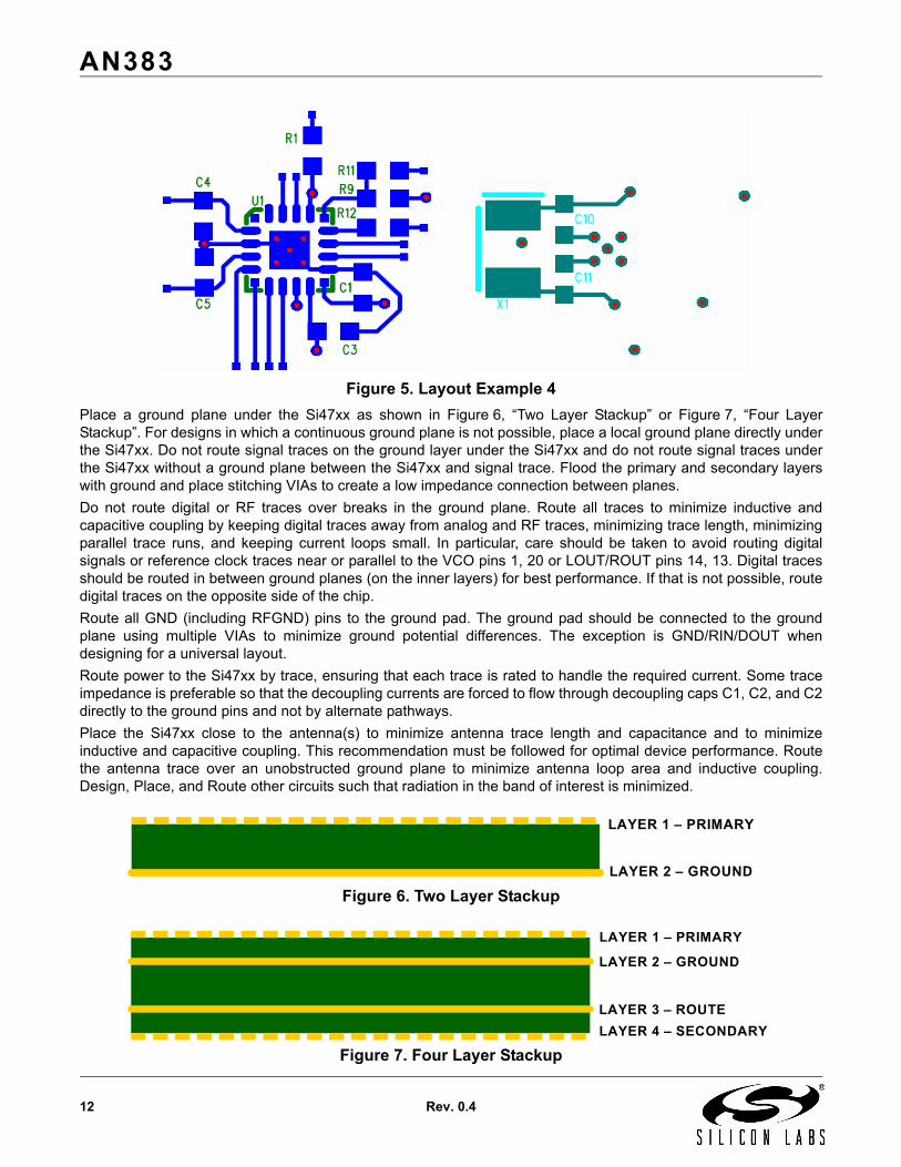
Figure 5. Layout Example 4Place a ground plane under the Si47xx as shown in Figure 6, “Two Layer Stackup” or Figure 7, “Four LayerStackup”. For designs in which a continuous ground plane is not possible, place a local ground plane directly underthe Si47xx. Do not route signal traces on the ground layer under the Si47xx and do not route signal traces underthe Si47xx without a ground plane between the Si47xx and signal trace. Flood the primary and secondary layerswith ground and place stitching VIAs to create a low impedance connection between planes.Do not route digital or RF traces over breaks in the ground plane. Route all traces to minimize inductive andcapacitive coupling by keeping digital traces away from analog and RF traces, minimizing trace length, minimizingparallel trace runs, and keeping current loops small. In particular, care should be taken to avoid routing digitalsignals or reference clock traces near or parallel to the VCO pins 1, 20 or LOUT/ROUT pins 14, 13. Digital tracesshould be routed in between ground planes (on the inner layers) for best performance. If that is not possible, routedigital traces on the opposite side of the chip.Route all GND (including RFGND) pins to the ground pad. The ground pad should be connected to the groundplane using multiple VIAs to minimize ground potential differences. The exception is GND/RIN/DOUT whendesigning for a universal layout.Route power to the Si47xx by trace, ensuring that each trace is rated to handle the required current. Some traceimpedance is preferable so that the decoupling currents are forced to flow through decoupling caps C1, C2, and C2directly to the ground pins and not by alternate pathways.Place the Si47xx close to the antenna(s) to minimize antenna trace length and capacitance and to minimizeinductive and capacitive coupling. This recommendation must be followed for optimal device performance. Routethe antenna trace over an unobstructed ground plane to minimize antenna loop area and inductive coupling.Design, Place, and Route other circuits such that radiation in the band of interest is minimized.
Figure 6. Two Layer Stackup
Figure 7. Four Layer Stackup
LAYER 2 – GROUND
LAYER 1 – PRIMARY
LAYER 1 – PRIMARY
LAYER 2 – GROUND
LAYER 3 – ROUTELAYER 4 – SECONDARY
AN383
Rev. 0.4 13
2.5. Si47xx 3x3 mm Design ChecklistThe following design checklist summarizes the guidelines presented in this section:
Place bypass caps C1, C2 and C3 as close as possible to the supply and ground pins.Place a VIA connecting C1, C2, and C3 to the power supplies such that the cap is between the Si47xx and the VIA.Route a wide, low inductance return current path from the C1, C2, and C3 to the Si47xx GND pins.Route GND/LIN/DOUT pin 15 to the GND pad if designing only for the Si4702/03. Place C4 as close as possible to FMI pin 2 and RFGND pin 3. Place a VIA connecting C4 to FMI on another layer as needed such that the cap is between Si47xx and the VIA.Route FMI pin 2 to GND if the pin functionality is not used.Place C5 following the guidelines for C4.Route TXO/AMI/LPI pin 4 to GND if the pin functionality is not used.Place resistor R1 as close to pin GPO3/DCLK 17 as possible.Place R9 as close as possible to VA/LIN/DFS pin16 as possible. Place resistor R11 as close to pin VA/LIN/DFS 16 as possible.Place resistor R12 as close to pin GND/RIN/DOUT 15 as possible.Place the series termination resistors R2–R6, R13–R16 as close to the host controller as possible.Place the crystal X1 as close to GPO3/DCLK pin 17 and RCLK pin 9 as possible.Route the SDIO trace and RCLK trace as far away from each other as possible when using crystal X1.Place caps C10 and C11 such that they share a common GND connection.Place a ground plane under the device as shown in Figure 6, “Two Layer Stackup” or Figure 7, “Four Layer Stackup”.Place a local ground plane directly under the device for designs in which a continuous ground plane is not possible.Route all traces to minimize inductive and capacitive coupling by keeping digital traces away from analog and RF traces, minimizing trace length, minimizing parallel trace runs, and keeping current loops small. Route digital traces in between ground plane for best performance. If that is not possible, route digital traces on the opposite side of the chip.Route all GND (including RFGND) pins to the ground pad. The ground pad should be connected to the ground plane using multiple VIAs minimize ground potential differences. The exception is GND/RIN/DOUT when designing for the universal layout.Route power to the Si47xx by trace, ensuring that each trace is rated to handle the required current. Do not route signal traces on the ground layer directly under the Si47xx.Do not route signal traces under the Si47xx without a ground plane between the Si47xx and signal trace. Do not route digital or RF traces over breaks in the ground plane. Do not route digital signals or reference clock traces near to the VCO pin 1 and 20 or the LOUT/ROUT output pin 14 and 13.Do not route VCO pin 1 and 20 (NC). These pins must be left floating to guarantee proper operation.Flood the primary and secondary layers with ground and place stitching VIAs.Place the Si47xx close to the antenna(s) to minimize antenna trace length and capacitance and to minimize inductive and capacitive coupling. This recommendation must be followed for optimal device performance.Route the antenna trace over an unobstructed ground plane to minimize antenna loop area and inductive coupling.Design, Place, and Route other circuits such that radiation in the band of interest is minimized.Tie unused pin(s) to GND, but do not tie No Connect (NC) pins to GND. For example, in Si471x FM transmitter analog audio input mode, DFS pin 14 and DIN pin 13 are not used; therefore, these two pins should be tied to GND.

AN383
14 Rev. 0.4
3. Headphone Antenna for FM Receive (Si470x/2x/3x Only)The Si470x/2x/3x FM Receiver component supports a headphone antenna interface through the FMI pin. Aheadphone antenna with a length between 1.1 and 1.45 m suits the FM application very well because it isapproximately half the FM wavelength (FM wavelength is ~3 m).
3.1. Headphone Antenna DesignA typical headphone cable will contain three or more conductors. The left and right audio channels are driven by aheadphone amplifier onto left and right audio conductors and the common audio conductor is used for the audioreturn path and FM antenna. Additional conductors may be used for microphone audio, switching, or otherfunctions, and in some applications the FM antenna will be a separate conductor within the cable. A representationof a typical application is shown in Figure 8, “Typical Headphone Antenna Application”.
Figure 8. Typical Headphone Antenna Application
Si47xx
Antenna
Left
Right
FerriteBeads
AN383
Rev. 0.4 15
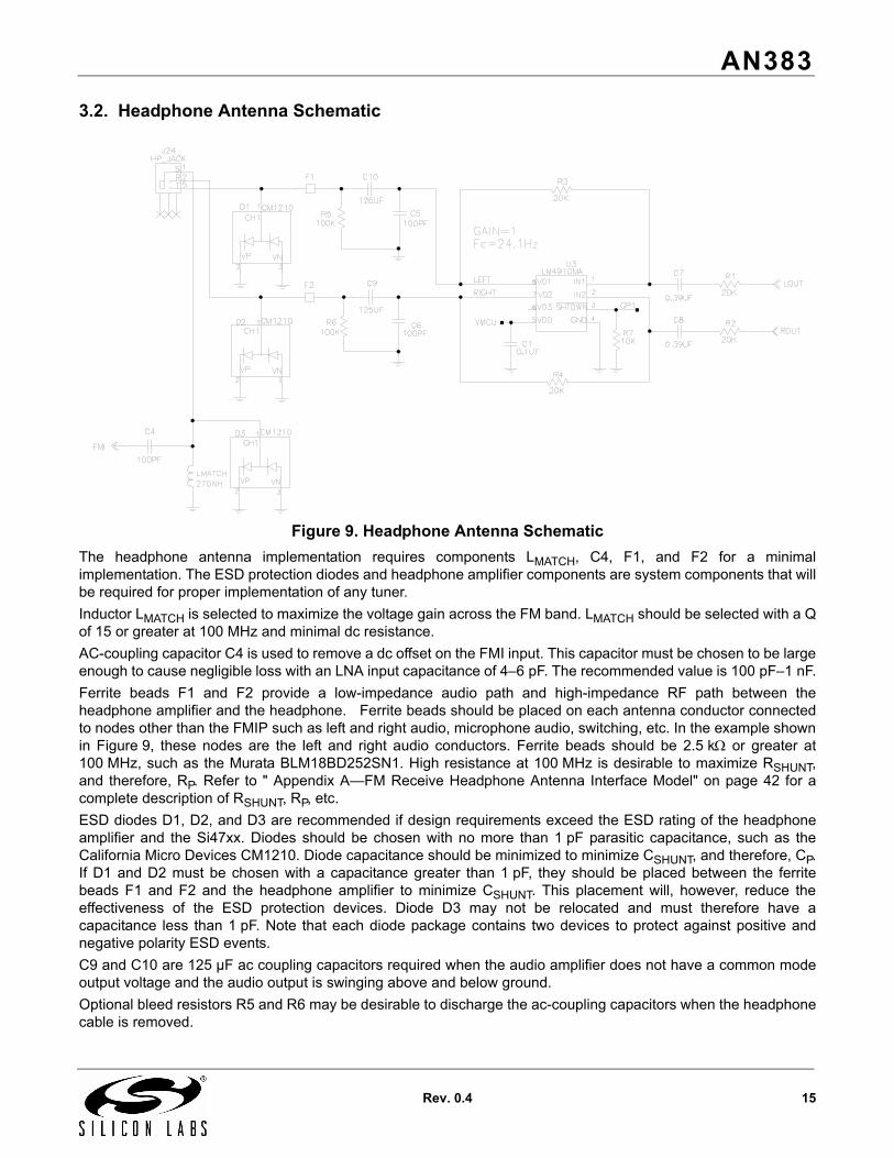
3.2. Headphone Antenna Schematic
Figure 9. Headphone Antenna SchematicThe headphone antenna implementation requires components LMATCH, C4, F1, and F2 for a minimalimplementation. The ESD protection diodes and headphone amplifier components are system components that willbe required for proper implementation of any tuner.Inductor LMATCH is selected to maximize the voltage gain across the FM band. LMATCH should be selected with a Qof 15 or greater at 100 MHz and minimal dc resistance.AC-coupling capacitor C4 is used to remove a dc offset on the FMI input. This capacitor must be chosen to be largeenough to cause negligible loss with an LNA input capacitance of 4–6 pF. The recommended value is 100 pF–1 nF.Ferrite beads F1 and F2 provide a low-impedance audio path and high-impedance RF path between theheadphone amplifier and the headphone. Ferrite beads should be placed on each antenna conductor connectedto nodes other than the FMIP such as left and right audio, microphone audio, switching, etc. In the example shownin Figure 9, these nodes are the left and right audio conductors. Ferrite beads should be 2.5 kΩ or greater at100 MHz, such as the Murata BLM18BD252SN1. High resistance at 100 MHz is desirable to maximize RSHUNT,and therefore, RP. Refer to " Appendix A—FM Receive Headphone Antenna Interface Model" on page 42 for acomplete description of RSHUNT, RP, etc.ESD diodes D1, D2, and D3 are recommended if design requirements exceed the ESD rating of the headphoneamplifier and the Si47xx. Diodes should be chosen with no more than 1 pF parasitic capacitance, such as theCalifornia Micro Devices CM1210. Diode capacitance should be minimized to minimize CSHUNT, and therefore, CP.If D1 and D2 must be chosen with a capacitance greater than 1 pF, they should be placed between the ferritebeads F1 and F2 and the headphone amplifier to minimize CSHUNT. This placement will, however, reduce theeffectiveness of the ESD protection devices. Diode D3 may not be relocated and must therefore have acapacitance less than 1 pF. Note that each diode package contains two devices to protect against positive andnegative polarity ESD events.C9 and C10 are 125 µF ac coupling capacitors required when the audio amplifier does not have a common modeoutput voltage and the audio output is swinging above and below ground.Optional bleed resistors R5 and R6 may be desirable to discharge the ac-coupling capacitors when the headphonecable is removed.
AN383
16 Rev. 0.4
Optional RF shunt capacitors C5 and C6 may be placed on the left and right audio traces at the headphoneamplifier output to reduce the level of digital noise passed to the antenna. The recommended value is 100 pF orgreater, however, the designer should confirm that the headphone amplifier is capable of driving the selected shuntcapacitance.This schematic example uses the National Semiconductor LM4910 headphone amplifier. Passive components R1–R4 and C7–C8 are required for the LM4910 headphone amplifier as described in the LM4910 data sheet. The gainof the right and left amplifiers is –R3/R1 and –R4/R2, respectively. These gains can be adjusted by changing thevalues of resistors R3 and R4. As a general guide, gain between 0.6 and 1.0 is recommended for the headphoneamplifier, depending on the gain of the headphone elements. Capacitors C7 and C8 are ac-coupling capacitorsrequired for the LM4910 interface. These capacitors, in conjunction with resistors R1 and R2, create a high-passfilter that sets the audio amplifier's lower frequency limit. The high-pass corner frequencies for the right and leftamplifiers are:
With the specified BOM components, the corner frequency of the headphone amplifier is approximately 20 Hz.Capacitor C1 is the supply bypass capacitor for the audio amplifier. The LM4910 can also be shut down byapplying a logic low voltage to the number 3 pin. The maximum logic low level is 0.4 V and the minimum logic highlevel is 1.5 V. The bill of materials for the typical application schematic shown in Figure 6 is provided in Table 7. Note thatmanufacturer is not critical for resistors and capacitors.
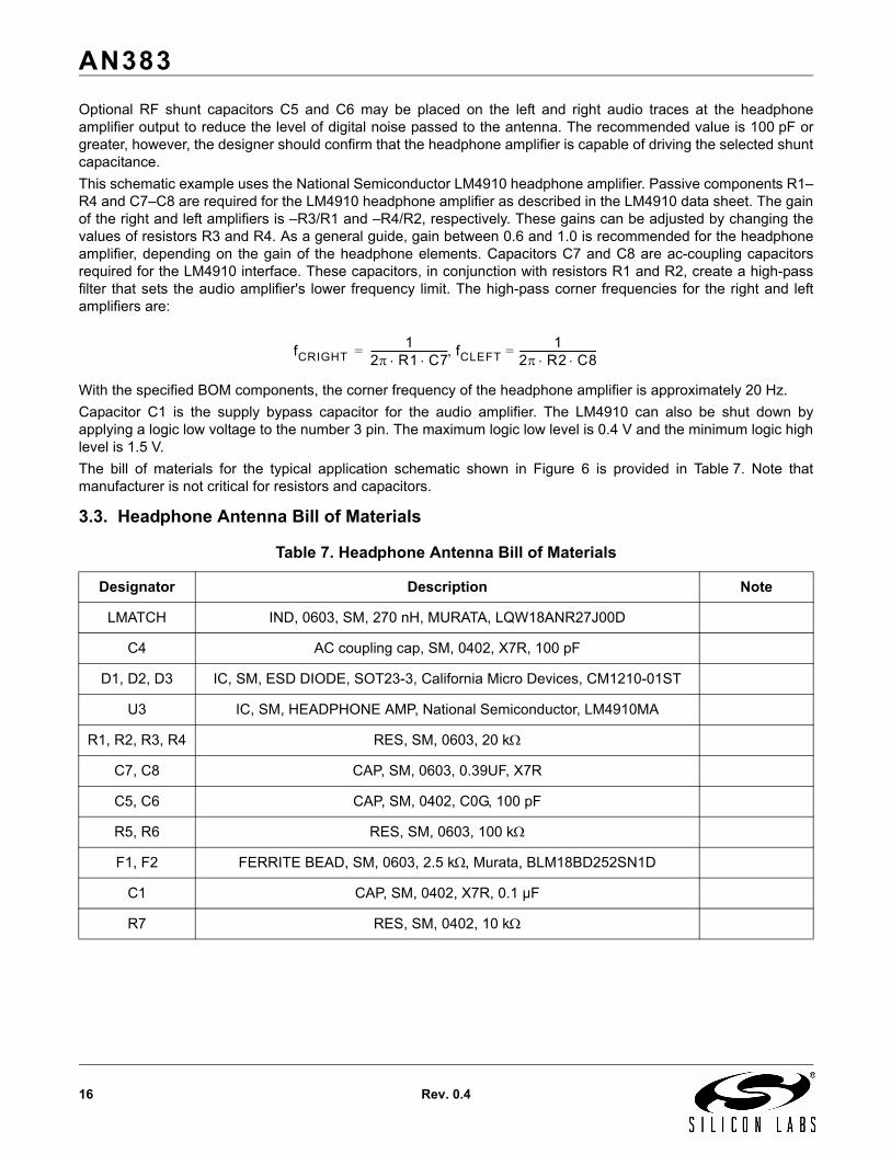
3.3. Headphone Antenna Bill of Materials
Table 7. Headphone Antenna Bill of Materials
Designator Description Note
LMATCH IND, 0603, SM, 270 nH, MURATA, LQW18ANR27J00D
C4 AC coupling cap, SM, 0402, X7R, 100 pF
D1, D2, D3 IC, SM, ESD DIODE, SOT23-3, California Micro Devices, CM1210-01ST
U3 IC, SM, HEADPHONE AMP, National Semiconductor, LM4910MA
R1, R2, R3, R4 RES, SM, 0603, 20 kΩ
C7, C8 CAP, SM, 0603, 0.39UF, X7R
C5, C6 CAP, SM, 0402, C0G, 100 pF
R5, R6 RES, SM, 0603, 100 kΩ
F1, F2 FERRITE BEAD, SM, 0603, 2.5 kΩ, Murata, BLM18BD252SN1D
C1 CAP, SM, 0402, X7R, 0.1 µF
R7 RES, SM, 0402, 10 kΩ
fCRIGHT1
2π R1 C7⋅ ⋅-------------------------------- fCLEFT
12π R2 C8⋅ ⋅--------------------------------=,=
AN383
Rev. 0.4 17
3.4. Headphone Antenna LayoutTo minimize inductive and capacitive coupling, inductor LMATCH and headphone jack J24 should be placed togetherand as far from noise sources such as clocks and digital circuits as possible. LMATCH should be placed near theheadphone connector to keep audio currents away from the Si47xx.To minimize CSHUNT and CP, place ferrite beads F1 and F2 as close as possible to the headphone connector.To maximize ESD protection diode effectiveness, place diodes D1, D2 and D3 as close as possible to theheadphone connector. If capacitance larger than 1 pF is required for D1 and D2, both components should beplaced between FB1 and FB2 and the headphone amplifier to minimize CSHUNT. Place the chip as close as possible to the headphone connector to minimize antenna trace capacitance,CPCBANT. Keep the trace length short and narrow and as far above the reference plane as possible, restrict thetrace to a microstrip topology (trace routes on the top or bottom PCB layers only), minimize trace vias, and relieveground fill on the trace layer. Note that minimizing capacitance has the effect of maximizing characteristicimpedance. It is not necessary to design for 50 Ω transmission lines.To reduce the level of digital noise passed to the antenna, RF shunt capacitors C5 and C6 may be placed on theleft and right audio traces close to the headphone amplifier audio output pins. The recommended value is 100 pFor greater, however, the designer should confirm that the headphone amplifier is capable of driving the selectedshunt capacitance.
3.5. Headphone Antenna Design ChecklistSelect an antenna length of 1.1 to 1.45 m.Select matching inductor LMATCH to maximize signal strength across the FM band.Select matching inductor LMATCH with a Q of 15 or greater at 100 MHz and minimal dc resistance.Place inductor LMATCH and headphone connector together and as far from potential noise sources as possible to reduce capacitive and inductive coupling.Place the Si47xx close to the headphone connector to minimize antenna trace length. Minimizing trace length reduces CP and the possibility for inductive and capacitive coupling into the antenna by noise sources. This recommendation must be followed for optimal device performance.Select ferrite beads F1–F2 with 2.5 kΩ or greater resistance at 100 MHz to maximize RSHUNT and, therefore, RP.Place ferrite beads F1-F2 close to the headphone connector.Select ESD diodes D1-D3 with minimum capacitance.Place ESD diodes D1-D3 as close as possible to the headphone connector for maximum effectiveness.Place optional RF shunt capacitors near the headphone amplifier’s left and right audio output pins to reduce the level of digital noise passed to the antenna.
AN383
18 Rev. 0.4
4. Embedded Antenna for FM Transmit and Receive(Si4704/05/06/1x/2x Only)
The FM Transmitter component on the Si471x/2x and the FM Receiver component on the Si4704/05/06/2x supportan embedded antenna interface through the TXO/LPI pin. In the case of the Si472x FM Transceiver, the sameembedded antenna can be used for both FM Transmit and Receive.
4.1. Embedded Antenna DesignAn embedded antenna can be designed using a loose wire, flex circuit, or PCB trace and can be categorized intotwo types: stub antenna and loop antenna. For the purpose of this application note, three types of embeddedantenna will be covered in detail:
Embedded stub (wire)Embedded loop (wire)Embedded stub (PCB trace)
The following table summarizes the advantages and disadvantages of these implementations.
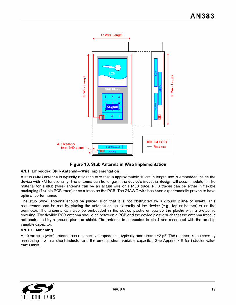
Figure 10 is an example of a stub antenna in wire implementation buried inside a cellular handset. Explanations ofthe dimensions A, B, C, and D are included later in this document.
Antenna Description Advantages DisadvantagesEmbedded Stub (Wire) Wire attached to or
molded inside product caseConnect to pin 4 for TX/RX
Placement flexibilityMinimum PCB spaceEasy to adjust length during design testing
Mechanical attachment to case requiredPerformance can be impacted by case shielding
Embedded Loop (Wire) Wire loop attached to or molded inside product caseConnect to pin 4 for TX/RX
Can achieve high efficiency per lengthPlacement flexibilityMinimum PCB spaceEasy to adjust length during design testing
Mechanical attachment to case requiredPerformance can be impacted by case shielding
Embedded Stub (PCB Trace)
Wire trace fabricated on outer PCB copper layerConnect to pin 4 for TX/RX
No mechanical attachment to caseEase of product assembly
PCB keep out regions required around antennaAdditional PCB spacePerformance can be impacted by case shielding
AN383
Rev. 0.4 19
Figure 10. Stub Antenna in Wire Implementation4.1.1. Embedded Stub Antenna—Wire ImplementationA stub (wire) antenna is typically a floating wire that is approximately 10 cm in length and is embedded inside thedevice with FM functionality. The antenna can be longer if the device's industrial design will accommodate it. Thematerial for a stub (wire) antenna can be an actual wire or a PCB trace. PCB traces can be either in flexiblepackaging (flexible PCB trace) or as a trace on the PCB. The 24AWG wire has been experimentally proven to haveoptimal performance.The stub (wire) antenna should be placed such that it is not obstructed by a ground plane or shield. Thisrequirement can be met by placing the antenna on an extremity of the device (e.g., top or bottom) or on theperimeter. The antenna can also be embedded in the device plastic or outside the plastic with a protectivecovering. The flexible PCB antenna should be between a PCB and the device plastic such that the antenna trace isnot obstructed by a ground plane or shield. The antenna is connected to pin 4 and resonated with the on-chipvariable capacitor.4.1.1.1. MatchingA 10 cm stub (wire) antenna has a capacitive impedance, typically more than 1~2 pF. The antenna is matched byresonating it with a shunt inductor and the on-chip shunt variable capacitor. See Appendix B for inductor valuecalculation.
AN383
20 Rev. 0.4
4.1.1.2. Configuration
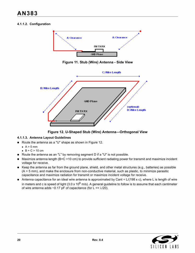
Figure 11. Stub (Wire) Antenna - Side View
Figure 12. U-Shaped Stub (Wire) Antenna—Orthogonal View4.1.1.3. Antenna Layout Guidelines
Route the antenna as a "U" shape as shown in Figure 12. A > 5 mm B + C > 10 cm
Route the antenna as an "L" by removing segment D if a "U" is not possible.Maximize antenna length (B+C >10 cm) to provide sufficient radiating power for transmit and maximize incident voltage for receive.Keep the antenna as far from the ground plane, shield, and other metal structures (e.g., batteries) as possible (A > 5 mm), and make the enclosure from non-conductive material, such as plastic, to minimize parasitic capacitance and maximize radiation for transmit or maximize incident voltage for receive. Antenna capacitance for an ideal wire antenna is approximated by Cant = L/(198 x c), where L is length of wire in meters and c is speed of light (3.0 x 10⁸ m/s). A general guideline to follow is to assume that each centimeter of wire antenna adds ~0.17 pF of capacitance (for L << λ/20).

AN383
Rev. 0.4 21
Use an ideal vertical wire antenna as a reference point to measure the performance of the wire antenna. Antenna capacitance will be larger and antenna performance will degrade in a practical application where the wire antenna is bent parallel to the GND plane.
4.1.2. Embedded Loop Antenna—Wire ImplementationA loop (wire) antenna is typically a floating wire that is approximately 13 cm or greater in circumference and isembedded inside the device with FM functionality. It is constructed with a floating wire or flexible PCB trace. Theshape of the antenna can be circular or rectangular with the goal of maximizing the enclosed area. The 24AWGhas been experimentally proven to have optimal performance. A floating wire antenna is typically embedded in theplastics, or outside of the plastics (with protective covering), at the perimeter of the device such that the antennatrace is not obstructed by the ground plane, shield, or other metal structures (e.g., batteries).Placement of the flexible PCB is typically between the main PCB and plastics such that the antenna trace is notobstructed by a ground plane or shield. A loop antenna is similar to a short wire antenna with the exception that theother end of the antenna is grounded. Because the other end is grounded, a loop antenna by itself is an inductor. 4.1.2.1. Antenna MatchingA loop (wire) antenna is an inductor of high impedance. The antenna is matched by resonating it with a shuntinductor or capacitor and the on-chip shunt variable capacitor.4.1.2.2. Configuration
Figure 13. Loop (Wire) Antenna—Side View
Length (cm) C Ant (pF)
10 1.68
11 1.85
12 2.02
13 2.19
14 2.36
15 2.53
AN383
22 Rev. 0.4
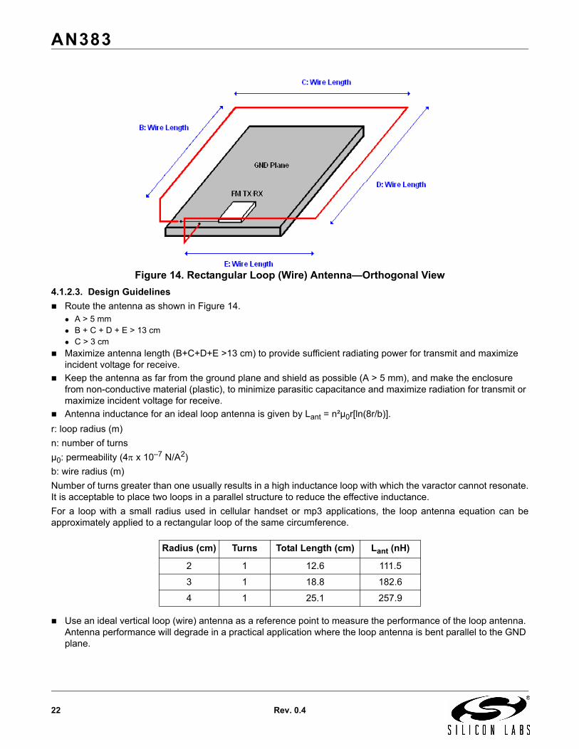
Figure 14. Rectangular Loop (Wire) Antenna—Orthogonal View4.1.2.3. Design Guidelines
Route the antenna as shown in Figure 14. A > 5 mm B + C + D + E > 13 cm C > 3 cm
Maximize antenna length (B+C+D+E >13 cm) to provide sufficient radiating power for transmit and maximize incident voltage for receive.Keep the antenna as far from the ground plane and shield as possible (A > 5 mm), and make the enclosure from non-conductive material (plastic), to minimize parasitic capacitance and maximize radiation for transmit or maximize incident voltage for receive.Antenna inductance for an ideal loop antenna is given by Lant = n²µ0r[ln(8r/b)].
r: loop radius (m)n: number of turnsµ0: permeability (4π x 10–7 N/A2)b: wire radius (m)Number of turns greater than one usually results in a high inductance loop with which the varactor cannot resonate.It is acceptable to place two loops in a parallel structure to reduce the effective inductance.For a loop with a small radius used in cellular handset or mp3 applications, the loop antenna equation can beapproximately applied to a rectangular loop of the same circumference.
Use an ideal vertical loop (wire) antenna as a reference point to measure the performance of the loop antenna. Antenna performance will degrade in a practical application where the loop antenna is bent parallel to the GND plane.
Radius (cm) Turns Total Length (cm) Lant (nH)
2 1 12.6 111.5
3 1 18.8 182.6
4 1 25.1 257.9
AN383
Rev. 0.4 23
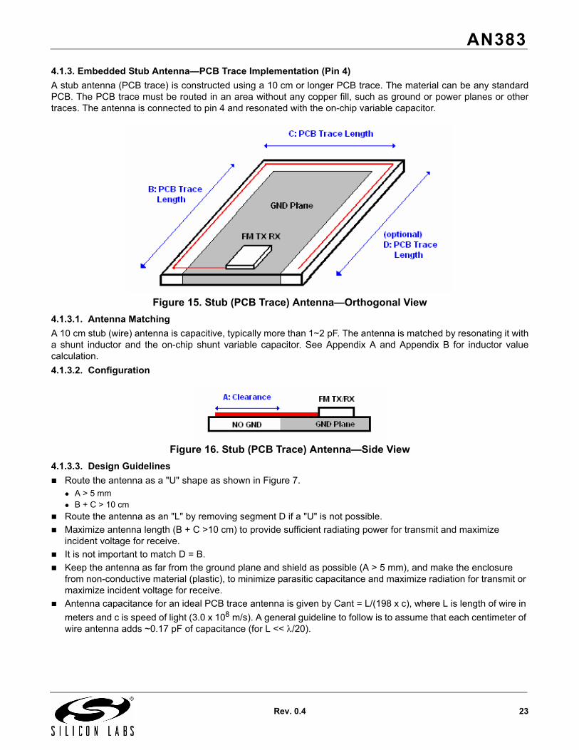
4.1.3. Embedded Stub Antenna—PCB Trace Implementation (Pin 4)A stub antenna (PCB trace) is constructed using a 10 cm or longer PCB trace. The material can be any standardPCB. The PCB trace must be routed in an area without any copper fill, such as ground or power planes or othertraces. The antenna is connected to pin 4 and resonated with the on-chip variable capacitor.
Figure 15. Stub (PCB Trace) Antenna—Orthogonal View4.1.3.1. Antenna MatchingA 10 cm stub (wire) antenna is capacitive, typically more than 1~2 pF. The antenna is matched by resonating it witha shunt inductor and the on-chip shunt variable capacitor. See Appendix A and Appendix B for inductor valuecalculation.4.1.3.2. Configuration
Figure 16. Stub (PCB Trace) Antenna—Side View4.1.3.3. Design Guidelines
Route the antenna as a "U" shape as shown in Figure 7. A > 5 mm B + C > 10 cm
Route the antenna as an "L" by removing segment D if a "U" is not possible.Maximize antenna length (B + C >10 cm) to provide sufficient radiating power for transmit and maximize incident voltage for receive.It is not important to match D = B.Keep the antenna as far from the ground plane and shield as possible (A > 5 mm), and make the enclosure from non-conductive material (plastic), to minimize parasitic capacitance and maximize radiation for transmit or maximize incident voltage for receive.Antenna capacitance for an ideal PCB trace antenna is given by Cant = L/(198 x c), where L is length of wire in meters and c is speed of light (3.0 x 10⁸ m/s). A general guideline to follow is to assume that each centimeter of wire antenna adds ~0.17 pF of capacitance (for L << λ/20).
AN383
24 Rev. 0.4
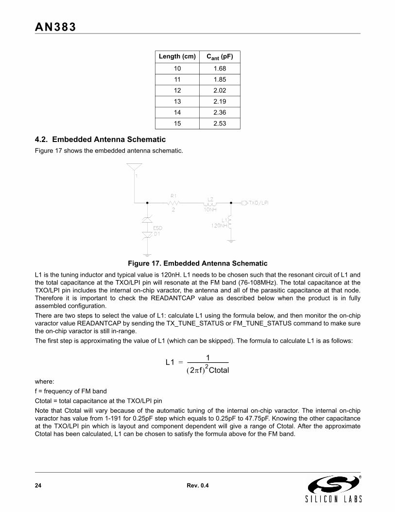
4.2. Embedded Antenna SchematicFigure 17 shows the embedded antenna schematic.
Figure 17. Embedded Antenna SchematicL1 is the tuning inductor and typical value is 120nH. L1 needs to be chosen such that the resonant circuit of L1 andthe total capacitance at the TXO/LPI pin will resonate at the FM band (76-108MHz). The total capacitance at theTXO/LPI pin includes the internal on-chip varactor, the antenna and all of the parasitic capacitance at that node.Therefore it is important to check the READANTCAP value as described below when the product is in fullyassembled configuration.There are two steps to select the value of L1: calculate L1 using the formula below, and then monitor the on-chipvaractor value READANTCAP by sending the TX_TUNE_STATUS or FM_TUNE_STATUS command to make surethe on-chip varactor is still in-range.The first step is approximating the value of L1 (which can be skipped). The formula to calculate L1 is as follows:
where:f = frequency of FM bandCtotal = total capacitance at the TXO/LPI pinNote that Ctotal will vary because of the automatic tuning of the internal on-chip varactor. The internal on-chipvaractor has value from 1-191 for 0.25pF step which equals to 0.25pF to 47.75pF. Knowing the other capacitanceat the TXO/LPI pin which is layout and component dependent will give a range of Ctotal. After the approximateCtotal has been calculated, L1 can be chosen to satisfy the formula above for the FM band.
Length (cm) Cant (pF)
10 1.68
11 1.85
12 2.02
13 2.19
14 2.36
15 2.53
L1 12πf( )2Ctotal--------------------------------=
AN383
Rev. 0.4 25
After choosing the right L1 value, the user is still required to check the on-chip varactor value READANTCAP bysending the TX_TUNE_STATUS or FM_TUNE_STATUS command to make sure that the on-chip varactor has notgone out-of-range. User also can jump to this second step right away and skip the first step of approximating L1 bytrying different values of L1.The procedure to monitor the READANTCAP is as follows:
Select at least three frequencies in the bottom, middle and top of the FM band (e.g. 88, 98, and 108 MHz) and get the READANTCAP values.It is even better if user sweeps the entire FM band and gets the READANTCAP values.L1 has a correct inductance value if 1 < READANTCAP < 191 READANTCAP at 88 MHz > READANTCAP at 98 MHz > READANTCAP at 108 MHz Be suspicious when READANTCAP returns the middle value of 97. It may be an indication that the inductor value is not
correct.L1 is not the right value and needs to be changed if either one of these three conditions occur: READANTCAP returns the bottom value of 1: it indicates that there is too much capacitance at the TXO/LPI pin. L1 needs
to be adjusted to a smaller value or the better solution is to try to reduce the parasitic capacitance at the TXO/LPI pin READANTCAP returns a middle value of 97: it indicates that there is way too much capacitance at the TXO/LPI pin. L1
needs to be adjusted to a smaller value or the better solution is to try to reduce the parasitic capacitance at the TXO/LPI pin READANTCAP returns the top value of 191: it indicates that there is too little of a capacitance at the TXO/LPI pin (unlikely
to happen). L1 needs to be adjusted to a bigger value.The rest of the components in the embedded antenna schematic are optional.L2 is the inductor to filter the 3–4 GHz VCO spurs and the recommended value is between 5 and 10 nH.D1 is the ESD diode and it is only necessary when there is an exposed pad going to the TXO/LPI pin.R1 is the ESD current limiting resistor and used in conjunction with D1. It is only necessary when there is anexposed pad going to the TXO/LPI pin.
4.3. Embedded Antenna Bill of Materials
4.4. Embedded Antenna LayoutThe placement of the chip going into the embedded antenna is critical. Place the chip as close as possible to theembedded antenna feedline. This will minimize the trace going to the embedded antenna which in turn willminimize parasitic capacitance. If long trace is needed between the TXO/LPI pin to the embedded antenna, keepthe trace as a microstrip topology where the trace is on the top or bottom layer. Do not bury the trace on the innerlayer. Relieve the ground fill along the trace which includes the ground fill on the inner layer. Note that the goal is tominimize the parasitic capacitance as much as possible, it is not necessary to design a 50 Ω transmission lines inthis applications because the embedded antenna is a high impedance antenna, and the parallel resonant circuit isalso high impedance at the resonant frequency.Put the optional ESD diode D1 and ESD current limiting resistor R1 as close to the embedded antenna as possibleto ensure optimal ESD performance.
Table 8. Embedded Antenna Bill of MaterialsDesignator Description Note
L1 Tuning inductor (typically 120 nH)L2 VCO filter inductor, 5–10 nH Optional
R1 Current limiting resistor for ESD, 2 Ω Optional, only needed if there is any exposed pad going to the TXO/LPI pin.
D1 ESD diode Optional, only needed if there is any exposed pad going to the TXO/LPI pin.
AN383
26 Rev. 0.4
4.5. Embedded Antenna Design ChecklistPlace the chip as close as possible to the embedded antenna feedline to minimize parasitic capacitance.Select tuning inductor L1 with a Q>30 to maximize both radiated and received power.Select tuning inductor L1 as large as possible to maximize radiated power and incident voltage.Place the antenna, and in particular the end of the antenna opposite the Si47xx as far from the ground plane as possible to maximize radiated and received power.Place inductor L1 and the Si47xx chip as far from potential noise sources as possible to reduce capacitive and inductive coupling.Place optional components L2 to filter VCO spurs if needed.Place optional components D1 and R1 to achieve 8 kV contact discharge ESD protection if the antenna is exposed.Select ESD diode D1 with minimum capacitance.
AN383
Rev. 0.4 27
5. Cable Antenna for FM Transmit and Receive (Si4704/05/06/1x/2x Only)This section describes how to interface the Si47xx FM to a cable antenna. An example of a cable antenna wouldbe a cigarette light adapter (CLA) cable or a bundled cable going to the consumer product that may contain powerconductors, audio signals, control signals, or any other auxiliary signals.
5.1. Cable Antenna DesignUsing a cable as the antenna for FM usually means that the signal has to be driven to and/or received from thecable shield or ground. This is because most cable will have a protective shield covering the inner wires. In thiscase, the capacitive coupling between the ground shield and all other conductors can be very large. As acomparison, capacitance of a three-conductor headphone cable is approximately 10–20 pF because headphonecable does not have ground shield and only has two conductors plus a ground conductor. However, thecapacitance from a cable antenna can be greater than 100–200 pF because of the ground shield and multipleconductors. This antenna capacitance can be reduced by placing ferrite beads on all conductor traces as shown inFigure 19. Minimizing antenna capacitance will maximize transmit and receive voltage. The following picture shows a Cigarette Light Adapter (CLA) cable that can be used as a cable antenna for FM.
Figure 18. Cigarette Lighter Adapter (CLA)
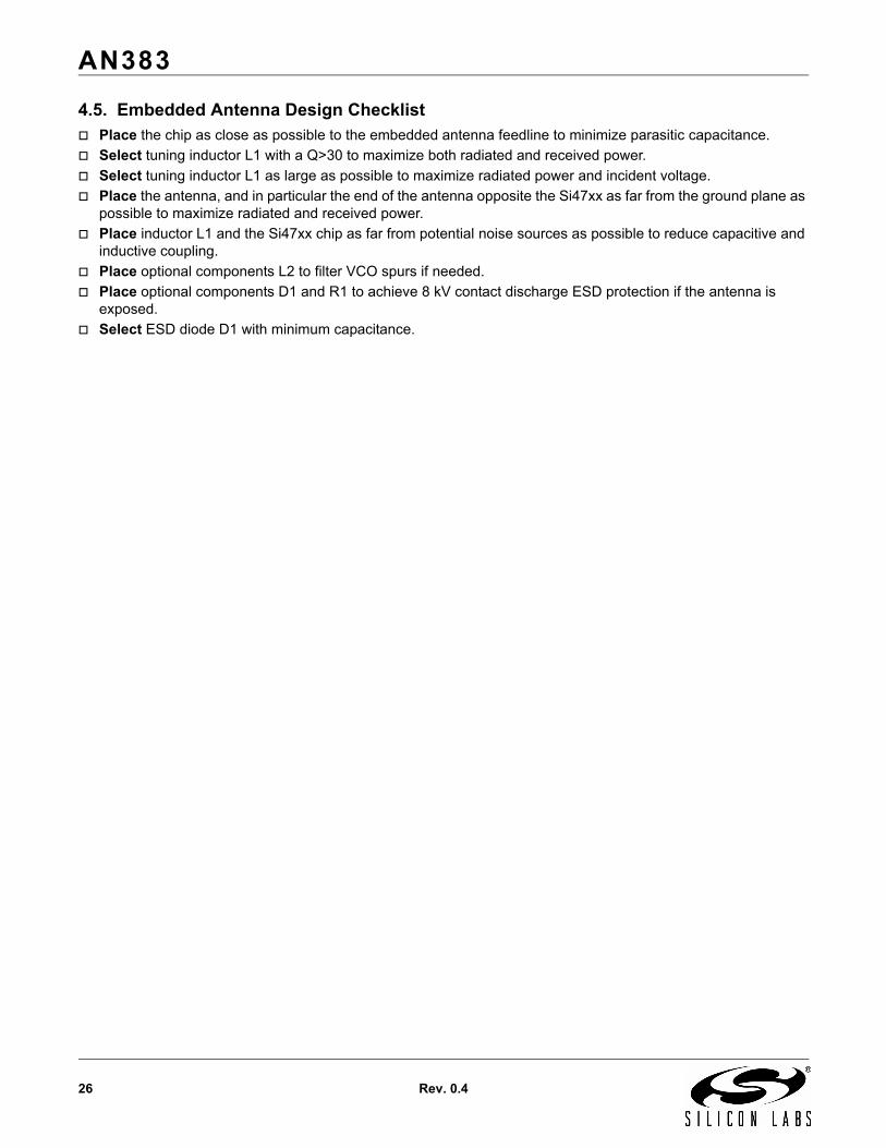
5.2. Cable Antenna Schematic
Figure 19. Cable Antenna SchematicL1 (12 0nH) is the tuning inductor for the transmitter and receiver and the return current path for transmitter. Theon-chip varactor can be configured to automatically resonate with the tuning inductor. Because of the largecapacitance, it is also generally hard to have a high-Q system with a cable antenna. A high-Q system is generallydesirable when using short antenna to maximize transmit and receive voltage. Fortunately, a high-Q system maynot be necessary for a cable antenna since the cable antenna is an efficient radiator and receiver. F1 (2.5 kΩ at 100 MHz) is a shunt ferrite to ground at the cable antenna side. A substantial amount of groundreturn current may flow through the cable antenna shield/ground because there are multiple conductors inside thecable along with power supply conductors. The ferrite will divert the ground return current of the cable antenna togo through the shunt ferrite rather than going through the tuning inductor and/or Si47xx chip.
AN383
28 Rev. 0.4
The important property of the shunt ferrite is its dc current carrying capability and this depends on what is themaximum current that the cable antenna can deliver. For example if the cable antenna can charge the accessoryconnected to it with a 1 A of current, then the shunt ferrite should have a dc current rating of greater than 1 A (e.g.,3 A). C1 (100 pF) is a dc blocking cap placed between the TXO/LPI pin and the cable antenna ground. The capacitor isused to isolate the cable return currents from the TXO/LPI pin.F2 (2.5 kΩ at 100 MHz) is a series ferrite placed on the signal conductor in the cable antenna. Note that seriesferrites should be placed on each signal conductor in the cable. The ferrite is used to isolate the signal conductorsfrom the shield/ground of the cable antenna and reduces parasitic capacitance seen by the shield/ground. Thechoice of the ferrite is dependent upon the type of signal on each individual conductor. If the conductor is used tocarry power, then a ferrite with a large dc current carrying capability should be used. If the conductor is used tocarry high frequency digital signals, make sure that the ferrite does not block the high frequency component ofthese signals. Likewise if the conductor is used to carry high frequency analog signals, make sure that the ferritedoes not filter the high frequency.
5.3. Cable Antenna Bill of MaterialsThe required bill of materials for the Figure 19 is shown in Table 9.
Table 9. Cable Antenna Bill of Materials
Designator Description Notes
L1 Tuning inductor, IND, 0603, SM, 120 nH, MURATA, LQW18ANR12J00D, Q>35
C1 DC blocking capacitor, SM, 0402, X7R, 100 pF
F1 Shunt Ferrite bead, FERRITEBEAD, SM, 0603, 470 Ω, 1 A, Murata, BLM18PG471SN1J
Rated dc current > max expected ground return current
F2 Series Ferrite bead, various types. Recommended ferrite for power lines:FERRITEBEAD, SM, 0603, 470 Ω, 1 A, Murata, BLM18PG471SN1J
Recommended ferrite for signals: FERRITEBEAD, SM, 0603, 2.5 kΩ, 50 mA Murata, BLM18BD252DN1D
For power signals, make sure the rated dc current > max expected ground return current.
For all other signals, make sure ferrite does not block/filter the high frequency component of the signals.

AN383
Rev. 0.4 29
5.4. Cable Antenna LayoutPlace the chip as close to the cable antenna as possible. This will minimize the trace length going to the cableantenna which will minimize the parasitic capacitance.Place the shunt ferrite for the ground return current as close to the cable as possible. Putting the shunt ferrite forthe ground return current close to the cable ensures that the ground return current has minimal loop which willreduce noise coupling. The series ferrites also should be put as close as possible to the cable. This will minimizethe parasitic capacitance seen by the TXO/LPI pin.
5.5. Cable Antenna Design ChecklistPlace the chip as close as possible to the cable antenna to minimize parasitic capacitance.Place the tuning inductor, L1, as far away from the noise source as possible.Make sure that the shunt ferrite has a dc rating that exceeds the expected max ground return current of the cable.Place the shunt ferrite close to the cable.Choose series ferrite that is appropriate for each type of signal in the conductor.Place the series ferrite(s) close to the cable.

AN383
30 Rev. 0.4
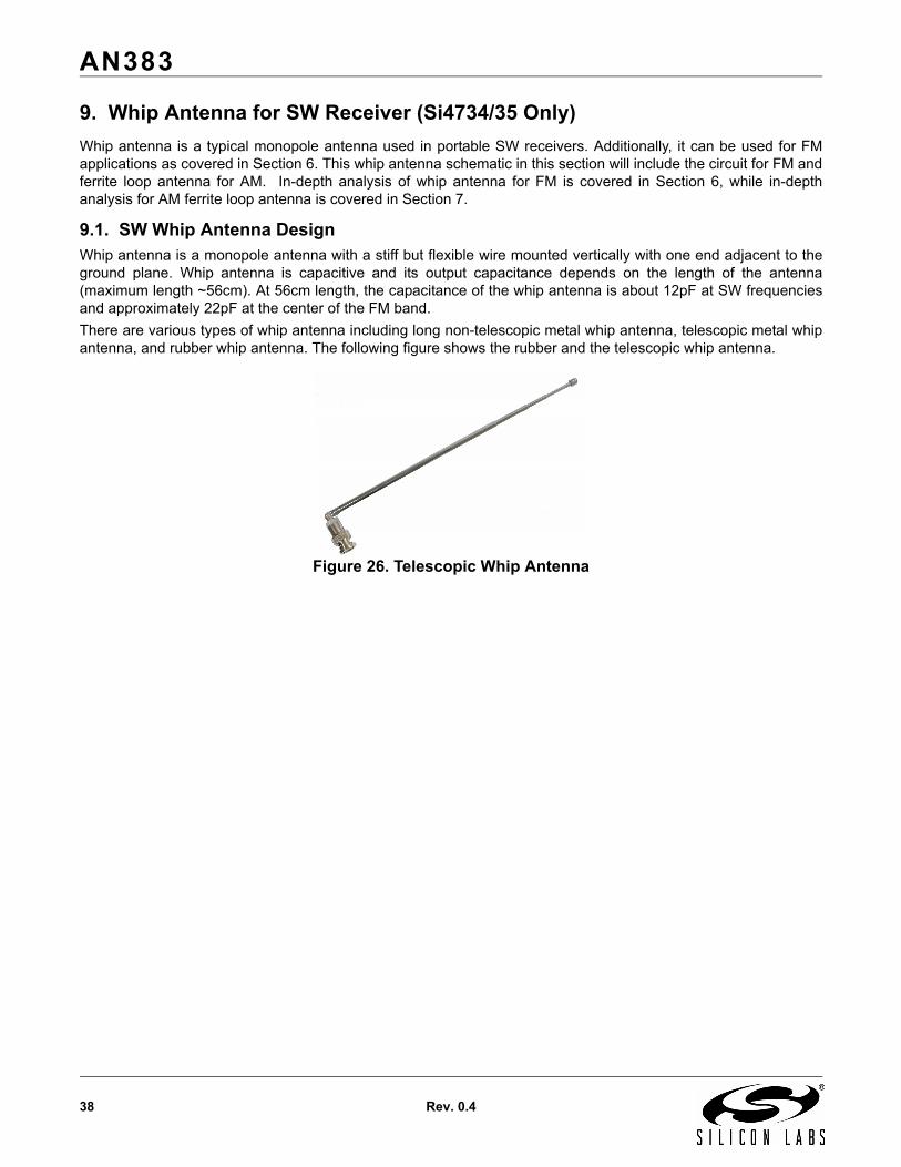
6. Whip Antenna for FM/WB Receiver (Si4736/37/38/39 Only)A whip antenna is a typical monopole antenna, which is used in portable weather band receivers. It can also beused for SW applications. For additional details, see "9. Whip Antenna for SW Receiver (Si4734/35 Only)" on page38.
6.1. FM/WB Whip Antenna DesignA whip antenna is a monopole antenna with a stiff but flexible wire mounted vertically with one end adjacent to theground plane.There are various types of whip antenna including long non-telescopic metal whip antenna, telescopic metal whipantenna, and rubber whip antenna. Figure 20 shows the rubber and the telescopic whip antenna.
Figure 20. Telescopic Whip AntennasThe whip antenna is capacitive, and its output capacitance depends on the length of the antenna (maximum length~56 cm). At 56 cm length, the capacitance of the whip antenna ranges from 18 pF to 32 pF for the US FM band.The antenna capacitance is about 22 pF in the center of the US FM band (98 MHz).
6.2. FM/WB Whip Antenna Schematic
Figure 21. FM/WB Whip AntennaL1 (56nH) is the matching inductor and it combines with the antenna impedance and the FMI impedance toresonate in the FM band.C5 (1nF) is the ac coupling cap going to the FMI pin.U3 is a required ESD diode since the antenna is exposed. The diode should be chosen with no more than 1pFparasitic capacitance, such as the California Micro Device CM1213.
AN383
Rev. 0.4 31
6.3. FM/WB Whip Antenna Bill of Materials
6.4. FM/WB Whip Antenna LayoutPlace the chip as close as possible to the whip antenna. This will minimize the trace length between the device andwhip antenna which in turn will minimize parasitic capacitance and the possibility of noise coupling. Place inductorL1 and the antenna connector together and as far from potential noise sources as possible and away from the I/Osignals of the Si4736/37/38/39. Place the ac coupling capacitor, C5, as close to the FMI pin as possible. Place ESDdiode U3 as close as possible to the whip antenna input connector for maximum effectiveness.
6.5. FM/WB Whip Antenna Design Checklist Maximize whip antenna length for optimal performance. Select matching inductor L1 with a Q of 15 or greater at 100MHz and minimal DC resistance. Select L1 inductor value to maximize resonance gain from FM frequency (88 MHz) to WB frequency (~162 MHz)Place L1 and whip antenna close together and as far from potential noise sources as possible to reduce capacitive and inductive coupling. Place the chip as close as possible to the whip antenna to minimize the antenna trace length. This reduces parasitic capacitance and hence reduces coupling into the antenna by noise sources. This recommendation must be followed for optimal device performance. Place ESD U3 as close as possible to the whip antenna for maximum effectiveness. Select ESD diode U3 with minimum capacitance.Place the ac coupling capacitor, C5, as close to the FMI pin as possible.
Table 10. FM/WB Whip Antenna Bill of Materials
Designator Description
WIP_ANTENNA Whip Antenna
L1 Tuning Inductor, 0603, SM, 56 nH, MURATA, LQW18AN56nJ00D
C5 AC coupling capacitor,1 nF, 10%, COG
U3 IC, SM, ESD DIODE, SOT23-3, Cali-fornia Micro Devices, CM1213-01ST
AN383
32 Rev. 0.4
7. Ferrite Loop Antenna for AM/LW Receive (Si4730/31/34/35/36/37 Only)There are two types of antenna that will work well for an AM receiver: a ferrite loop antenna or an air loop antenna.A ferrite loop antenna can be placed internally on the device or externally to the device with a wire connection.When the ferrite loop antenna is placed internally on the device, it is more susceptible to picking up any noisewithin the device. When the ferrite loop antenna is placed outside a device, e.g., at the end of an extension cable,it is less prone to device noise activity and may result in better AM reception.
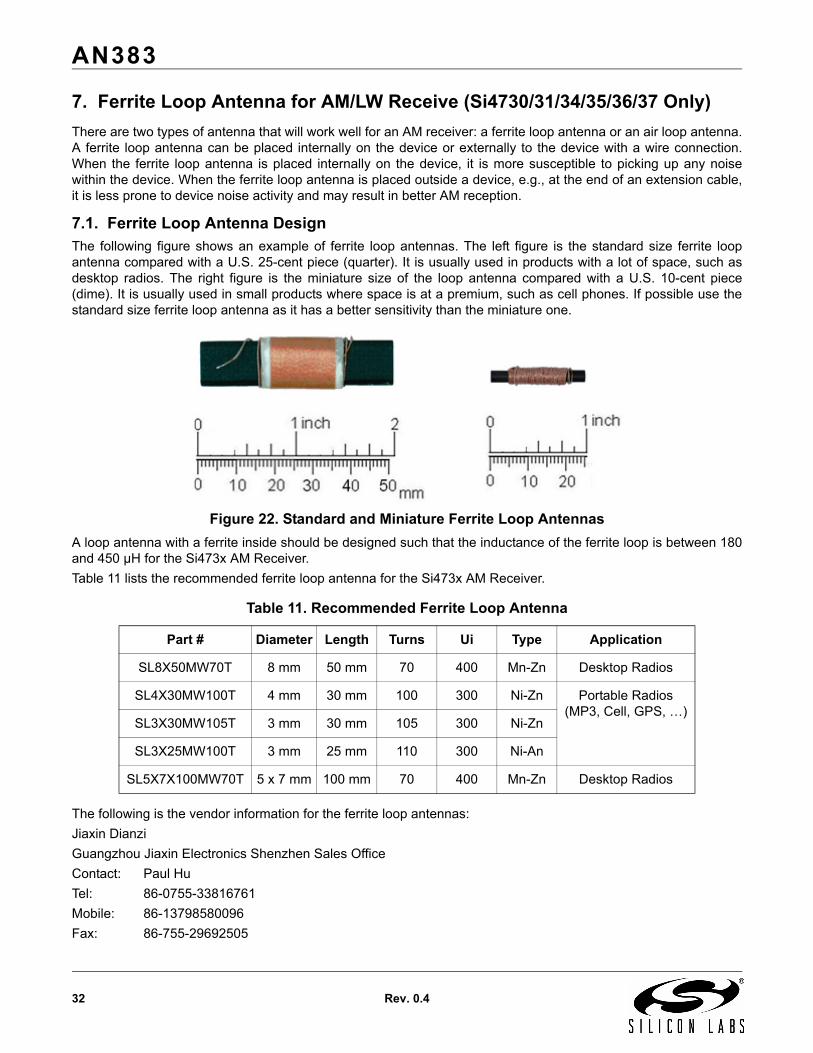
7.1. Ferrite Loop Antenna DesignThe following figure shows an example of ferrite loop antennas. The left figure is the standard size ferrite loopantenna compared with a U.S. 25-cent piece (quarter). It is usually used in products with a lot of space, such asdesktop radios. The right figure is the miniature size of the loop antenna compared with a U.S. 10-cent piece(dime). It is usually used in small products where space is at a premium, such as cell phones. If possible use thestandard size ferrite loop antenna as it has a better sensitivity than the miniature one.
Figure 22. Standard and Miniature Ferrite Loop AntennasA loop antenna with a ferrite inside should be designed such that the inductance of the ferrite loop is between 180and 450 µH for the Si473x AM Receiver.Table 11 lists the recommended ferrite loop antenna for the Si473x AM Receiver.
The following is the vendor information for the ferrite loop antennas:Jiaxin Dianzi Guangzhou Jiaxin Electronics Shenzhen Sales OfficeContact: Paul HuTel: 86-0755-33816761Mobile: 86-13798580096Fax: 86-755-29692505
Table 11. Recommended Ferrite Loop Antenna
Part # Diameter Length Turns Ui Type Application
SL8X50MW70T 8 mm 50 mm 70 400 Mn-Zn Desktop Radios
SL4X30MW100T 4 mm 30 mm 100 300 Ni-Zn Portable Radios (MP3, Cell, GPS, …)
SL3X30MW105T 3 mm 30 mm 105 300 Ni-Zn
SL3X25MW100T 3 mm 25 mm 110 300 Ni-An
SL5X7X100MW70T 5 x 7 mm 100 mm 70 400 Mn-Zn Desktop Radios
AN383
Rev. 0.4 33
email: [email protected]: www.firstantenna.comAddress: F/2 Building D, SaJin, Bao'an District,
Shenzhen Guangdong 518108,China
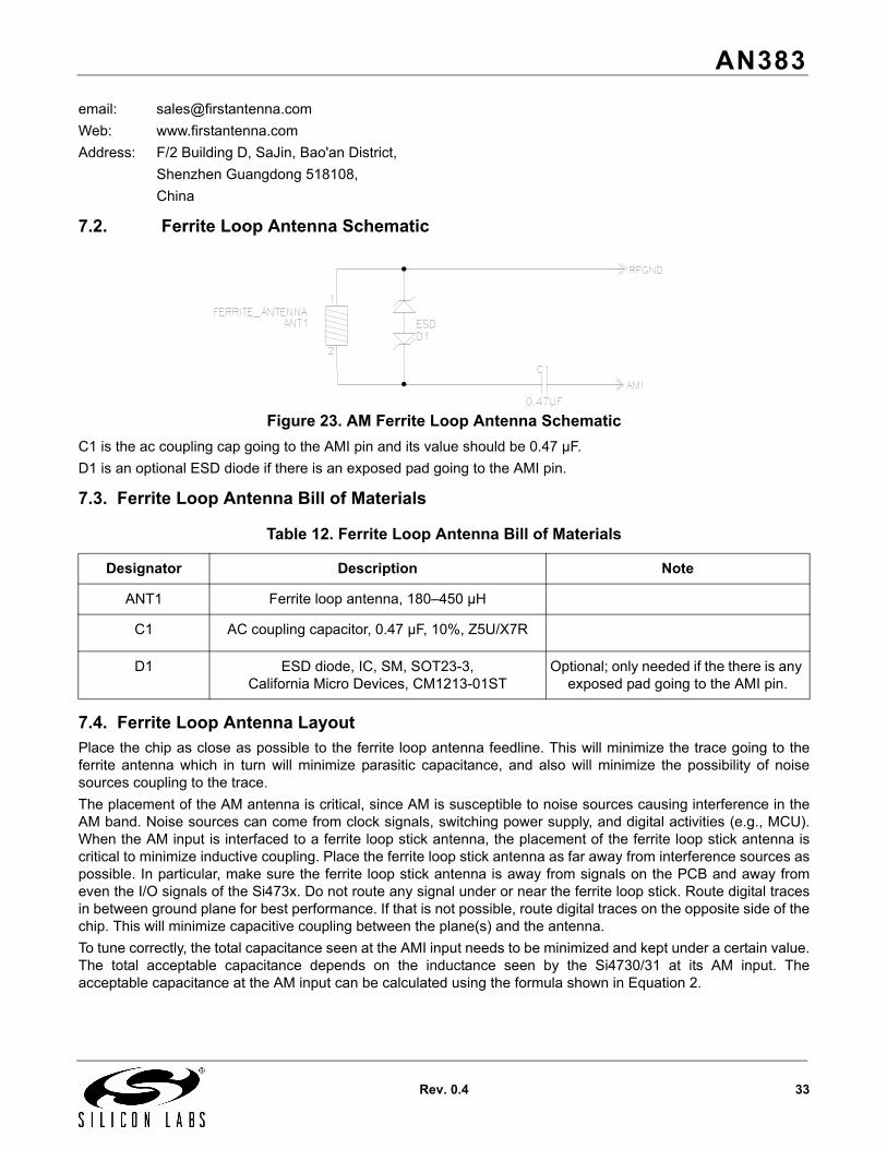
7.2. Ferrite Loop Antenna Schematic
Figure 23. AM Ferrite Loop Antenna SchematicC1 is the ac coupling cap going to the AMI pin and its value should be 0.47 µF.D1 is an optional ESD diode if there is an exposed pad going to the AMI pin.
7.3. Ferrite Loop Antenna Bill of Materials
7.4. Ferrite Loop Antenna LayoutPlace the chip as close as possible to the ferrite loop antenna feedline. This will minimize the trace going to theferrite antenna which in turn will minimize parasitic capacitance, and also will minimize the possibility of noisesources coupling to the trace.The placement of the AM antenna is critical, since AM is susceptible to noise sources causing interference in theAM band. Noise sources can come from clock signals, switching power supply, and digital activities (e.g., MCU).When the AM input is interfaced to a ferrite loop stick antenna, the placement of the ferrite loop stick antenna iscritical to minimize inductive coupling. Place the ferrite loop stick antenna as far away from interference sources aspossible. In particular, make sure the ferrite loop stick antenna is away from signals on the PCB and away fromeven the I/O signals of the Si473x. Do not route any signal under or near the ferrite loop stick. Route digital tracesin between ground plane for best performance. If that is not possible, route digital traces on the opposite side of thechip. This will minimize capacitive coupling between the plane(s) and the antenna.To tune correctly, the total capacitance seen at the AMI input needs to be minimized and kept under a certain value.The total acceptable capacitance depends on the inductance seen by the Si4730/31 at its AM input. Theacceptable capacitance at the AM input can be calculated using the formula shown in Equation 2.
Table 12. Ferrite Loop Antenna Bill of Materials
Designator Description Note
ANT1 Ferrite loop antenna, 180–450 µH
C1 AC coupling capacitor, 0.47 µF, 10%, Z5U/X7R
D1 ESD diode, IC, SM, SOT23-3,California Micro Devices, CM1213-01ST
Optional; only needed if the there is any exposed pad going to the AMI pin.
AN383
34 Rev. 0.4
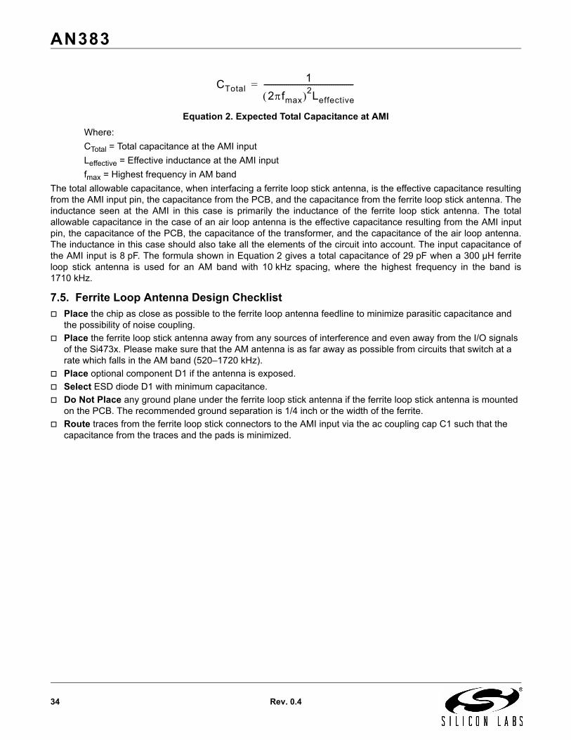
Equation 2. Expected Total Capacitance at AMIWhere:CTotal = Total capacitance at the AMI inputLeffective = Effective inductance at the AMI inputfmax = Highest frequency in AM band
The total allowable capacitance, when interfacing a ferrite loop stick antenna, is the effective capacitance resultingfrom the AMI input pin, the capacitance from the PCB, and the capacitance from the ferrite loop stick antenna. Theinductance seen at the AMI in this case is primarily the inductance of the ferrite loop stick antenna. The totalallowable capacitance in the case of an air loop antenna is the effective capacitance resulting from the AMI inputpin, the capacitance of the PCB, the capacitance of the transformer, and the capacitance of the air loop antenna.The inductance in this case should also take all the elements of the circuit into account. The input capacitance ofthe AMI input is 8 pF. The formula shown in Equation 2 gives a total capacitance of 29 pF when a 300 µH ferriteloop stick antenna is used for an AM band with 10 kHz spacing, where the highest frequency in the band is1710 kHz.
7.5. Ferrite Loop Antenna Design ChecklistPlace the chip as close as possible to the ferrite loop antenna feedline to minimize parasitic capacitance and the possibility of noise coupling.Place the ferrite loop stick antenna away from any sources of interference and even away from the I/O signals of the Si473x. Please make sure that the AM antenna is as far away as possible from circuits that switch at a rate which falls in the AM band (520–1720 kHz).Place optional component D1 if the antenna is exposed.Select ESD diode D1 with minimum capacitance.Do Not Place any ground plane under the ferrite loop stick antenna if the ferrite loop stick antenna is mounted on the PCB. The recommended ground separation is 1/4 inch or the width of the ferrite.Route traces from the ferrite loop stick connectors to the AMI input via the ac coupling cap C1 such that the capacitance from the traces and the pads is minimized.
CTotal1
2πfmax( )2Leffective
------------------------------------------------=
AN383
Rev. 0.4 35
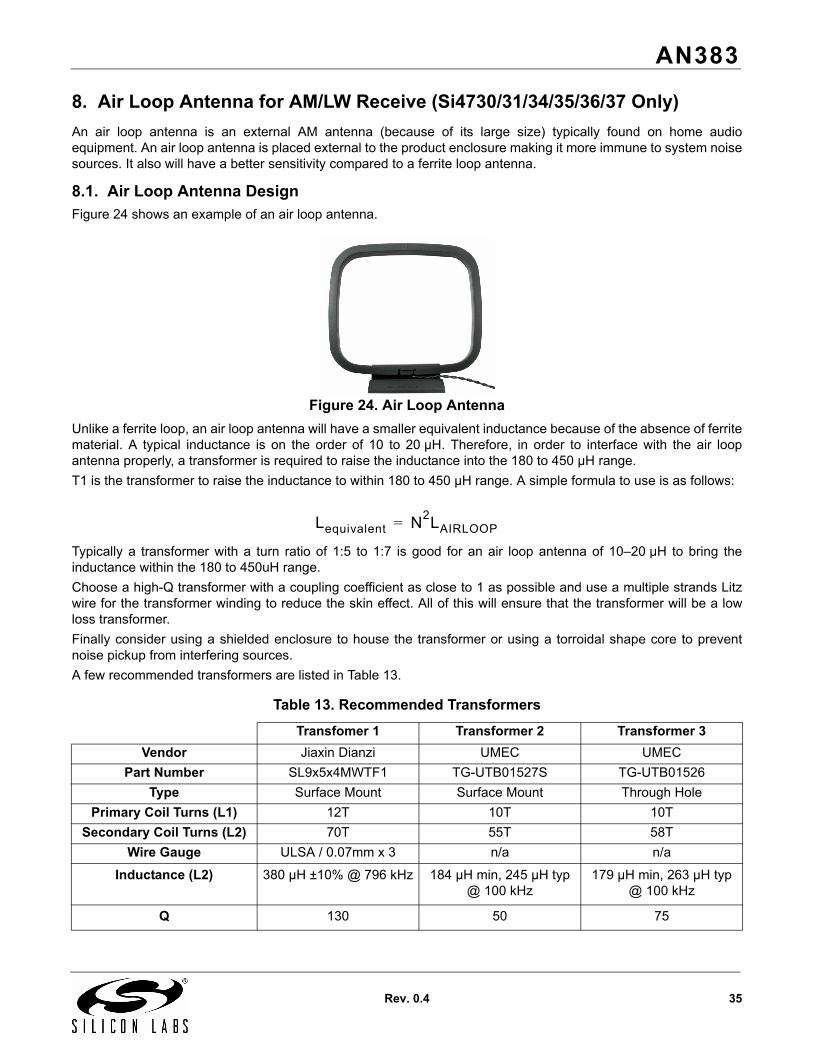
8. Air Loop Antenna for AM/LW Receive (Si4730/31/34/35/36/37 Only)An air loop antenna is an external AM antenna (because of its large size) typically found on home audioequipment. An air loop antenna is placed external to the product enclosure making it more immune to system noisesources. It also will have a better sensitivity compared to a ferrite loop antenna.
8.1. Air Loop Antenna DesignFigure 24 shows an example of an air loop antenna.
Figure 24. Air Loop AntennaUnlike a ferrite loop, an air loop antenna will have a smaller equivalent inductance because of the absence of ferritematerial. A typical inductance is on the order of 10 to 20 µH. Therefore, in order to interface with the air loopantenna properly, a transformer is required to raise the inductance into the 180 to 450 µH range.T1 is the transformer to raise the inductance to within 180 to 450 µH range. A simple formula to use is as follows:
Typically a transformer with a turn ratio of 1:5 to 1:7 is good for an air loop antenna of 10–20 µH to bring theinductance within the 180 to 450uH range.Choose a high-Q transformer with a coupling coefficient as close to 1 as possible and use a multiple strands Litzwire for the transformer winding to reduce the skin effect. All of this will ensure that the transformer will be a lowloss transformer.Finally consider using a shielded enclosure to house the transformer or using a torroidal shape core to preventnoise pickup from interfering sources.A few recommended transformers are listed in Table 13.
Table 13. Recommended Transformers
Transfomer 1 Transformer 2 Transformer 3Vendor Jiaxin Dianzi UMEC UMEC
Part Number SL9x5x4MWTF1 TG-UTB01527S TG-UTB01526Type Surface Mount Surface Mount Through Hole
Primary Coil Turns (L1) 12T 10T 10TSecondary Coil Turns (L2) 70T 55T 58T
Wire Gauge ULSA / 0.07mm x 3 n/a n/a
Inductance (L2) 380 µH ±10% @ 796 kHz 184 µH min, 245 µH typ @ 100 kHz
179 µH min, 263 µH typ @ 100 kHz
Q 130 50 75
Lequivalent N2LAIRLOOP=
AN383
36 Rev. 0.4
The following is the vendor information for the above transformer:Vendor #1:Jiaxin DianziGuangzhou Jiaxin Electronics Shenzhen Sales OfficeContact:Paul HuTel: 86-0755-33816761Mobile: 86-13798580096Fax: 86-755-29692505email: [email protected]: www.firstantenna.comAddress: F/2 Building D, SaJin, Bao'an District,
Shenzhen Guangdong 518108,China
Vendor #2:UMEC USA, Inc.Website: www.umec-usa.com
www.umec.com.tw
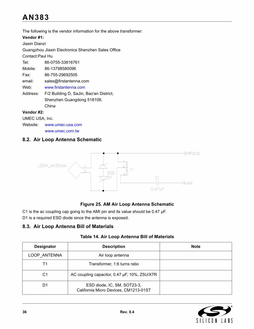
8.2. Air Loop Antenna Schematic
Figure 25. AM Air Loop Antenna SchematicC1 is the ac coupling cap going to the AMI pin and its value should be 0.47 µF.D1 is a required ESD diode since the antenna is exposed.
8.3. Air Loop Antenna Bill of Materials
Table 14. Air Loop Antenna Bill of Materials
Designator Description Note
LOOP_ANTENNA Air loop antenna
T1 Transformer, 1:6 turns ratio
C1 AC coupling capacitor, 0.47 µF, 10%, Z5U/X7R
D1 ESD diode, IC, SM, SOT23-3,California Micro Devices, CM1213-01ST

AN383
Rev. 0.4 37
8.4. Air Loop Antenna LayoutPlace the chip and the transformer as close as possible to the air loop antenna feedline. This will minimize thetrace going to the air loop antenna which in turn will minimize parasitic capacitance and the possibility of noisecoupling.When an air loop antenna with a transformer is used with the Si473x, minimize inductive coupling by making surethat the transformer is placed away from all sources of interference. Keep the transformer away from signals on thePCB and away from even the I/O signals of the Si473x. Do not route any signals under or near the transformer.Use a shielded transformer if possible.
8.5. Air Loop Antenna Design ChecklistSelect a shielded transformer or a torroidal shape transformer to prevent noise pickup from interfering sourcesSelect a high-Q transformer with coupling coefficient as close to 1 as possibleUse multiple strands Litz wire for the transformer windingPlace the transformer away from any sources of interference and even away from the I/O signals of the Si473x. Please make sure that the AM antenna is as far away as possible from circuits that switch at a rate which falls in the AM band (520–1720 kHz).Route traces from the transformer to the AMI input via the ac coupling cap C1 such that the capacitance from the traces and the pads is minimized.Select ESD diode D1 with minimum capacitance.
AN383
38 Rev. 0.4
9. Whip Antenna for SW Receiver (Si4734/35 Only)Whip antenna is a typical monopole antenna used in portable SW receivers. Additionally, it can be used for FMapplications as covered in Section 6. This whip antenna schematic in this section will include the circuit for FM andferrite loop antenna for AM. In-depth analysis of whip antenna for FM is covered in Section 6, while in-depthanalysis for AM ferrite loop antenna is covered in Section 7.
9.1. SW Whip Antenna DesignWhip antenna is a monopole antenna with a stiff but flexible wire mounted vertically with one end adjacent to theground plane. Whip antenna is capacitive and its output capacitance depends on the length of the antenna(maximum length ~56cm). At 56cm length, the capacitance of the whip antenna is about 12pF at SW frequenciesand approximately 22pF at the center of the FM band. There are various types of whip antenna including long non-telescopic metal whip antenna, telescopic metal whipantenna, and rubber whip antenna. The following figure shows the rubber and the telescopic whip antenna.
Figure 26. Telescopic Whip Antenna
AN383
Rev. 0.4 39
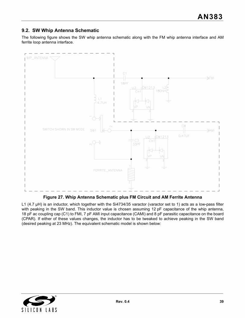
9.2. SW Whip Antenna SchematicThe following figure shows the SW whip antenna schematic along with the FM whip antenna interface and AMferrite loop antenna interface.
Figure 27. Whip Antenna Schematic plus FM Circuit and AM Ferrite AntennaL1 (4.7 µH) is an inductor, which together with the Si4734/35 varactor (varactor set to 1) acts as a low-pass filterwith peaking in the SW band. This inductor value is chosen assuming 12 pF capacitance of the whip antenna,18 pF ac coupling cap (C1) to FMI, 7 pF AMI input capacitance (CAMI) and 8 pF parasitic capacitance on the board(CPAR). If either of these values changes, the inductor has to be tweaked to achieve peaking in the SW band(desired peaking at 23 MHz). The equivalent schematic model is shown below:
AN383
40 Rev. 0.4
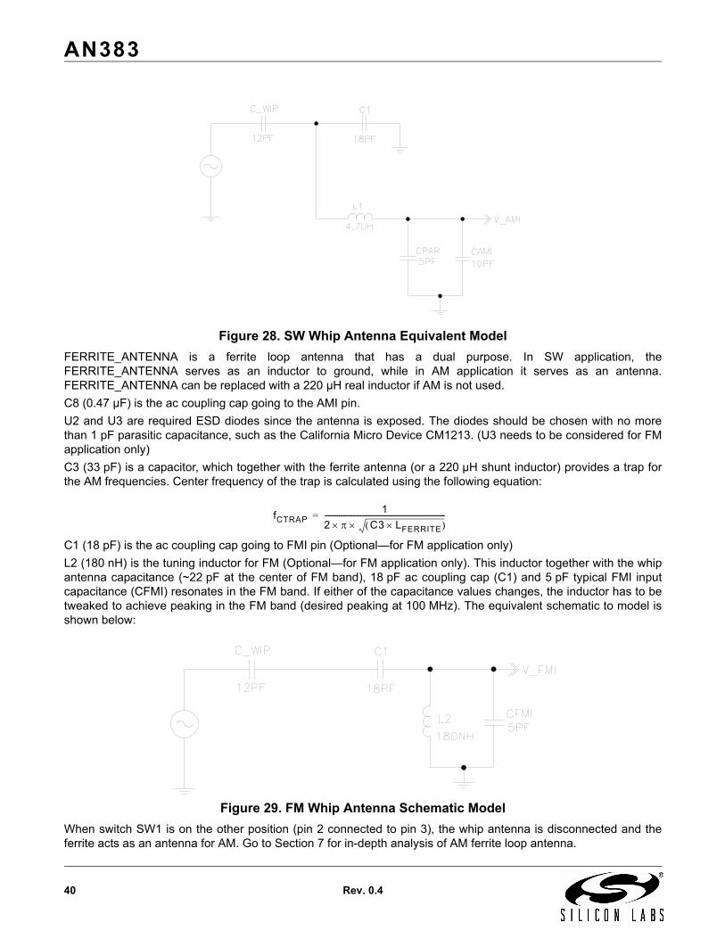
Figure 28. SW Whip Antenna Equivalent ModelFERRITE_ANTENNA is a ferrite loop antenna that has a dual purpose. In SW application, theFERRITE_ANTENNA serves as an inductor to ground, while in AM application it serves as an antenna.FERRITE_ANTENNA can be replaced with a 220 µH real inductor if AM is not used.C8 (0.47 µF) is the ac coupling cap going to the AMI pin.U2 and U3 are required ESD diodes since the antenna is exposed. The diodes should be chosen with no morethan 1 pF parasitic capacitance, such as the California Micro Device CM1213. (U3 needs to be considered for FMapplication only)C3 (33 pF) is a capacitor, which together with the ferrite antenna (or a 220 µH shunt inductor) provides a trap forthe AM frequencies. Center frequency of the trap is calculated using the following equation:
C1 (18 pF) is the ac coupling cap going to FMI pin (Optional—for FM application only)L2 (180 nH) is the tuning inductor for FM (Optional—for FM application only). This inductor together with the whipantenna capacitance (~22 pF at the center of FM band), 18 pF ac coupling cap (C1) and 5 pF typical FMI inputcapacitance (CFMI) resonates in the FM band. If either of the capacitance values changes, the inductor has to betweaked to achieve peaking in the FM band (desired peaking at 100 MHz). The equivalent schematic to model isshown below:
Figure 29. FM Whip Antenna Schematic ModelWhen switch SW1 is on the other position (pin 2 connected to pin 3), the whip antenna is disconnected and theferrite acts as an antenna for AM. Go to Section 7 for in-depth analysis of AM ferrite loop antenna.
fCTRAP1
2 π C3 LFERRITE×( )××--------------------------------------------------------------------=
AN383
Rev. 0.4 41
9.3. SW Whip Antenna Bill of Materials
9.4. SW Whip Antenna LayoutPlace the chip as close as possible to the whip antenna. This will minimize the trace length between the device andwhip antenna which in turn will minimize parasitic capacitance and the possibility of noise coupling. Place the whipantenna away from any sources of interference and away from the I/O signals of the Si4734/35. Place the accoupling capacitor, C8, as close to the AMI pin as possible. Place the ac coupling capacitor, C1, as close aspossible to the FMI pin. Place ESD diodes U2 and U3 as close as possible to the whip antenna input connector formaximum effectiveness.
9.5. SW Whip Antenna Design ChecklistMaximize whip antenna length for optimal performance.Select matching inductor L1 with a Q of 20 or greater at 25 MHz and minimal dc resistance.Select L1 inductor value to maximize signal strength across the FM band.Place L1 and whip antenna close together and as far from potential noise sources as possible to reduce capacitive and inductive coupling.Place the chip as close as possible to the whip antenna to minimize the antenna trace length. This reduces parasitic capacitance and hence reduces coupling into the antenna by noise sources. This recommendation must be followed for optimal device performance.Place ESD diodes U2 and U3 as close as possible to the whip antenna for maximum effectiveness.Select ESD diodes U2 and U3 with minimum capacitance.Place the ac coupling capacitor, C8, as close to the AMI pin as possible.Follow the design checklist in "7. Ferrite Loop Antenna for AM/LW Receive (Si4730/31/34/35/36/37 Only)" on page 32 for the ferrite antenna to optimize AM performance (if AM is used in addition to SW).
Designator Description Notes
WIP_ANTENNA Whip Antenna
L1 Low Pass Filter Inductor, 1008, SM, 4.7 µH, COILCRAFT,
1008CS-472GLB
Q of 20 or greater at 25 MHz and minimal DC resistance.
SW1 SPDT Switch Optional, only needed if the design requires switching between AM and SW.Not required for SW only applications.
C3 Capacitor, 33 pF, 5%, COG
C8 AC coupling capacitor, 0.47 µF, 10%, Z5U/X7R
FERRITE_ANTENNA AM Antenna Optional, can be replaced with a 220 µH shunt inductor for SW only applications
U2, U3 IC, SM, ESD DIODE, SOT23-3, California Micro Devices,
CM1213-01ST
C1 Capacitor, 18 pF, 5%, COG Optional, only for FM
L2 Ind, 0603, SM, 180 nH, MURATA, LQW18ANR18J00D
Optional, only for FM
AN383
42 Rev. 0.4
APPENDIX A—FM RECEIVE HEADPHONE ANTENNA INTERFACE MODEL
The simplified circuit model for the headphone antenna interface shown in Figure 30, “Headphone Antenna andMatching Network Model”, and includes the headphone antenna, matching inductor, PCB and Si4700/01 LNA. Thissection discusses maximizing voltage gain across the FM band at the LNA input by varying headphone antennaand PCB parameters, and selecting the optimal matching inductor. It is very important to note that the performanceis optimized by maximizing input voltage, not power.
Figure 30. Headphone Antenna and Matching Network ModelRANT - Antenna ResistanceCANT - Antenna CapacitanceLMATCH - Inductance MatchCPCBANT - PCB Antenna Trace CapacitanceRSHUNT - Shunt Resistance of Ferrites CSHUNT - Audio Conductor Shunt CapacitanceCLNA - LNA CapacitanceRLNA - LNA Resistance
The headphone antenna and matching network model can be further simplified and represented in the form of aparallel resonant RLC circuit as shown in Figure 31, “Parallel Resonant RLC Circuit Model”. In this simplified modelthe parallel resistance, RP, represents the antenna resistance, RANT, the shunt resistance of ferrites on the left andright audio conductors, RSHUNT, and the LNA resistance, RLNA. The parallel capacitance, CP, represents theantenna capacitance, CANT, PCB antenna trace capacitance, CPCBANT, audio conductor shunt capacitance,CSHUNT, and LNA capacitance, CLNA.
LMATCH
RANT
CPCBANT RSHUNT CLNA RLNA
Headphone Antenna PCB FM Receive LNA
CSHUNT
CANT
Match
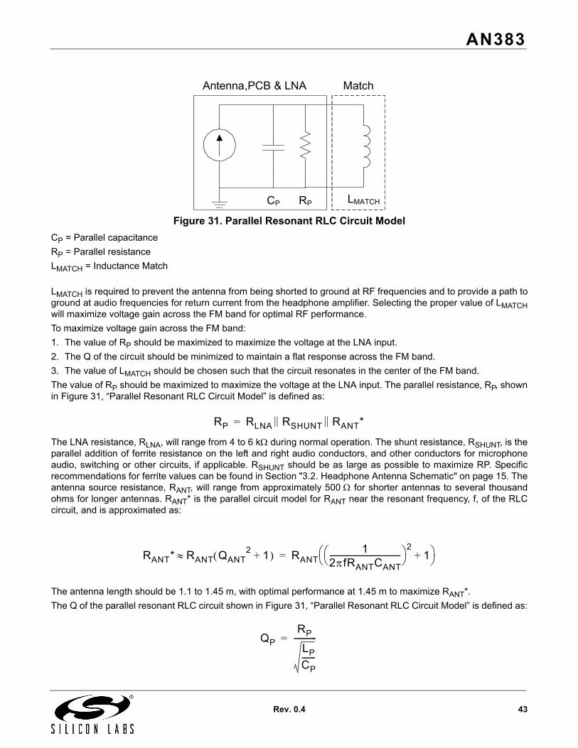
AN383
Rev. 0.4 43
Figure 31. Parallel Resonant RLC Circuit ModelCP = Parallel capacitanceRP = Parallel resistanceLMATCH = Inductance Match
LMATCH is required to prevent the antenna from being shorted to ground at RF frequencies and to provide a path toground at audio frequencies for return current from the headphone amplifier. Selecting the proper value of LMATCHwill maximize voltage gain across the FM band for optimal RF performance.To maximize voltage gain across the FM band:1. The value of RP should be maximized to maximize the voltage at the LNA input.2. The Q of the circuit should be minimized to maintain a flat response across the FM band.3. The value of LMATCH should be chosen such that the circuit resonates in the center of the FM band.The value of RP should be maximized to maximize the voltage at the LNA input. The parallel resistance, RP, shownin Figure 31, “Parallel Resonant RLC Circuit Model” is defined as:
The LNA resistance, RLNA, will range from 4 to 6 kΩ during normal operation. The shunt resistance, RSHUNT, is theparallel addition of ferrite resistance on the left and right audio conductors, and other conductors for microphoneaudio, switching or other circuits, if applicable. RSHUNT should be as large as possible to maximize RP. Specificrecommendations for ferrite values can be found in Section "3.2. Headphone Antenna Schematic" on page 15. Theantenna source resistance, RANT, will range from approximately 500 Ω for shorter antennas to several thousandohms for longer antennas. RANT* is the parallel circuit model for RANT near the resonant frequency, f, of the RLCcircuit, and is approximated as:
The antenna length should be 1.1 to 1.45 m, with optimal performance at 1.45 m to maximize RANT*.The Q of the parallel resonant RLC circuit shown in Figure 31, “Parallel Resonant RLC Circuit Model” is defined as:
LMATCHCP RP
MatchAntenna,PCB & LNA
RP RLNA RSHUNT RANT*|| ||=
RANT* RANT QANT2 1+( )≈ RANT
12πfRANTCANT-------------------------------------⎝ ⎠⎛ ⎞ 2
1+⎝ ⎠⎛ ⎞=
QPRP
LPCP-------
------------=
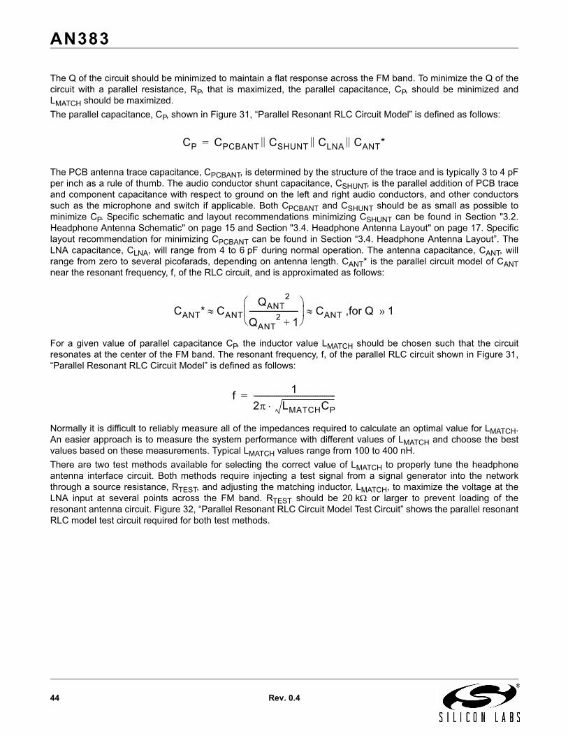
AN383
44 Rev. 0.4
The Q of the circuit should be minimized to maintain a flat response across the FM band. To minimize the Q of thecircuit with a parallel resistance, RP, that is maximized, the parallel capacitance, CP, should be minimized andLMATCH should be maximized.The parallel capacitance, CP, shown in Figure 31, “Parallel Resonant RLC Circuit Model” is defined as follows:
The PCB antenna trace capacitance, CPCBANT, is determined by the structure of the trace and is typically 3 to 4 pFper inch as a rule of thumb. The audio conductor shunt capacitance, CSHUNT, is the parallel addition of PCB traceand component capacitance with respect to ground on the left and right audio conductors, and other conductorssuch as the microphone and switch if applicable. Both CPCBANT and CSHUNT should be as small as possible tominimize CP. Specific schematic and layout recommendations minimizing CSHUNT can be found in Section "3.2.Headphone Antenna Schematic" on page 15 and Section "3.4. Headphone Antenna Layout" on page 17. Specificlayout recommendation for minimizing CPCBANT can be found in Section “3.4. Headphone Antenna Layout”. TheLNA capacitance, CLNA, will range from 4 to 6 pF during normal operation. The antenna capacitance, CANT, willrange from zero to several picofarads, depending on antenna length. CANT* is the parallel circuit model of CANTnear the resonant frequency, f, of the RLC circuit, and is approximated as follows:
For a given value of parallel capacitance CP, the inductor value LMATCH should be chosen such that the circuitresonates at the center of the FM band. The resonant frequency, f, of the parallel RLC circuit shown in Figure 31,“Parallel Resonant RLC Circuit Model” is defined as follows:
Normally it is difficult to reliably measure all of the impedances required to calculate an optimal value for LMATCH.An easier approach is to measure the system performance with different values of LMATCH and choose the bestvalues based on these measurements. Typical LMATCH values range from 100 to 400 nH.There are two test methods available for selecting the correct value of LMATCH to properly tune the headphoneantenna interface circuit. Both methods require injecting a test signal from a signal generator into the networkthrough a source resistance, RTEST, and adjusting the matching inductor, LMATCH, to maximize the voltage at theLNA input at several points across the FM band. RTEST should be 20 kΩ or larger to prevent loading of theresonant antenna circuit. Figure 32, “Parallel Resonant RLC Circuit Model Test Circuit” shows the parallel resonantRLC model test circuit required for both test methods.
CP CPCBANT CSHUNT CLNA CANT*|| || ||=
CANT* CANTQANT
2
QANT2 1+
--------------------------⎝ ⎠⎜ ⎟⎛ ⎞
CANT ,for Q 1»≈ ≈
f 12π LMATCHCP⋅--------------------------------------------=
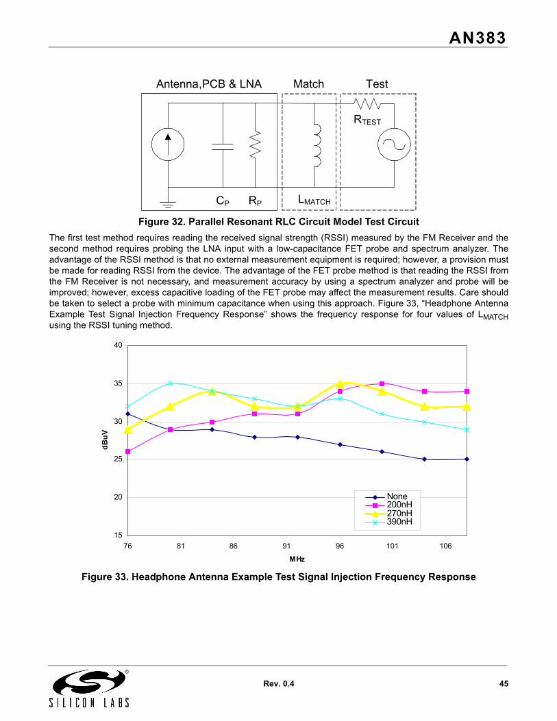
AN383
Rev. 0.4 45
Figure 32. Parallel Resonant RLC Circuit Model Test CircuitThe first test method requires reading the received signal strength (RSSI) measured by the FM Receiver and thesecond method requires probing the LNA input with a low-capacitance FET probe and spectrum analyzer. Theadvantage of the RSSI method is that no external measurement equipment is required; however, a provision mustbe made for reading RSSI from the device. The advantage of the FET probe method is that reading the RSSI fromthe FM Receiver is not necessary, and measurement accuracy by using a spectrum analyzer and probe will beimproved; however, excess capacitive loading of the FET probe may affect the measurement results. Care shouldbe taken to select a probe with minimum capacitance when using this approach. Figure 33, “Headphone AntennaExample Test Signal Injection Frequency Response” shows the frequency response for four values of LMATCHusing the RSSI tuning method.
Figure 33. Headphone Antenna Example Test Signal Injection Frequency Response
LMATCHCP RP
MatchAntenna,PCB & LNA
RTEST
Test
15
20
25
30
35
40
76 81 86 91 96 101 106
MHz
dBuV
None200nH270nH390nH
AN383
46 Rev. 0.4
It is clear from Figure 33, “Headphone Antenna Example Test Signal Injection Frequency Response” that thematching inductor, LMATCH, is preferred to no matching inductor, however, selecting the best value for LMATCHcan be difficult by inspection.Select the optimal value for LMATCH by following these guidelines:1. The mean value of RSSI should be maximized.2. The standard deviation of RSSI should be minimized.Table 15 shows 270 nH is the optimal choice for LMATCH because it maximizes the mean RSSI and minimizes theRSSI standard deviation.
Table 15. Headphone Antenna Example Test Signal Injection Mean and Standard Deviation
200 nH 270 nH 390 nH
Mean (dB) 31.5 32.4 32.1
Standard Deviation (dB) 3.0 1.7 1.9
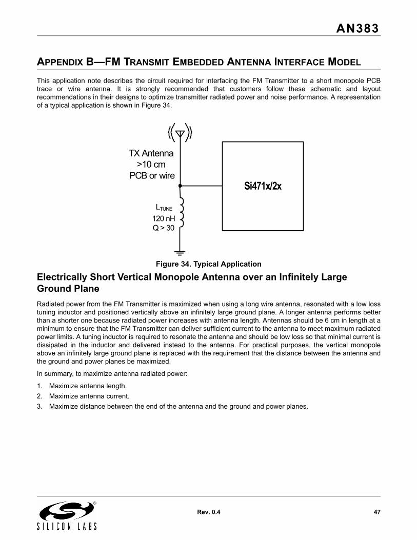
AN383
Rev. 0.4 47
APPENDIX B—FM TRANSMIT EMBEDDED ANTENNA INTERFACE MODEL
This application note describes the circuit required for interfacing the FM Transmitter to a short monopole PCBtrace or wire antenna. It is strongly recommended that customers follow these schematic and layoutrecommendations in their designs to optimize transmitter radiated power and noise performance. A representationof a typical application is shown in Figure 34.
Figure 34. Typical Application
Electrically Short Vertical Monopole Antenna over an Infinitely Large Ground PlaneRadiated power from the FM Transmitter is maximized when using a long wire antenna, resonated with a low losstuning inductor and positioned vertically above an infinitely large ground plane. A longer antenna performs betterthan a shorter one because radiated power increases with antenna length. Antennas should be 6 cm in length at aminimum to ensure that the FM Transmitter can deliver sufficient current to the antenna to meet maximum radiatedpower limits. A tuning inductor is required to resonate the antenna and should be low loss so that minimal current isdissipated in the inductor and delivered instead to the antenna. For practical purposes, the vertical monopoleabove an infinitely large ground plane is replaced with the requirement that the distance between the antenna andthe ground and power planes be maximized.
In summary, to maximize antenna radiated power:
1. Maximize antenna length.2. Maximize antenna current.3. Maximize distance between the end of the antenna and the ground and power planes.
Si471x/2x
TX Antenna>10 cm
PCB or wire
LTUNE
120 nHQ > 30
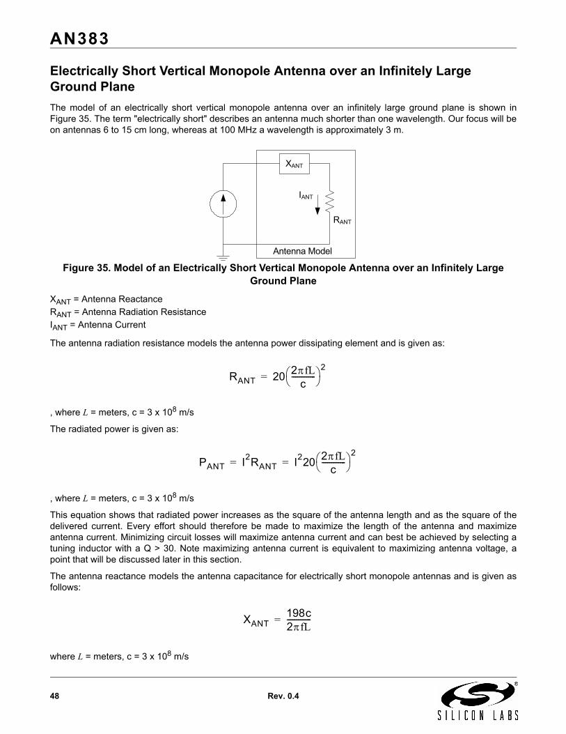
AN383
48 Rev. 0.4
Electrically Short Vertical Monopole Antenna over an Infinitely Large Ground PlaneThe model of an electrically short vertical monopole antenna over an infinitely large ground plane is shown inFigure 35. The term "electrically short" describes an antenna much shorter than one wavelength. Our focus will beon antennas 6 to 15 cm long, whereas at 100 MHz a wavelength is approximately 3 m.
Figure 35. Model of an Electrically Short Vertical Monopole Antenna over an Infinitely Large Ground Plane
XANT = Antenna ReactanceRANT = Antenna Radiation ResistanceIANT = Antenna Current
The antenna radiation resistance models the antenna power dissipating element and is given as:
, where L = meters, c = 3 x 10⁸ m/s
The radiated power is given as:
, where L = meters, c = 3 x 10⁸ m/s
This equation shows that radiated power increases as the square of the antenna length and as the square of thedelivered current. Every effort should therefore be made to maximize the length of the antenna and maximizeantenna current. Minimizing circuit losses will maximize antenna current and can best be achieved by selecting atuning inductor with a Q > 30. Note maximizing antenna current is equivalent to maximizing antenna voltage, apoint that will be discussed later in this section.
The antenna reactance models the antenna capacitance for electrically short monopole antennas and is given asfollows:
where L = meters, c = 3 x 10⁸ m/s
RANT
XANT
Antenna Model
IANT
RANT 20 2πfLc
-------------⎝ ⎠⎛ ⎞ 2
=
PANT I2RANT I220 2πfLc
-------------⎝ ⎠⎛ ⎞ 2
= =
XANT198c2πfL-------------=
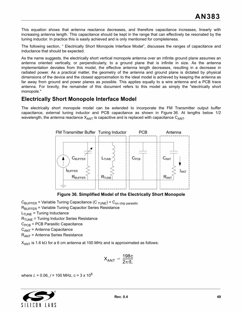
AN383
Rev. 0.4 49
This equation shows that antenna reactance decreases, and therefore capacitance increases, linearly withincreasing antenna length. This capacitance should be kept in the range that can effectively be resonated by thetuning inductor. In practice this is easily achieved and is only mentioned for completeness.
The following section, “ Electrically Short Monopole Interface Model”, discusses the ranges of capacitance andinductance that should be expected.
As the name suggests, the electrically short vertical monopole antenna over an infinite ground plane assumes anantenna oriented vertically, or perpendicularly, to a ground plane that is infinite in size. As the antennaimplementation deviates from this model, the effective antenna length decreases, resulting in a decrease inradiated power. As a practical matter, the geometry of the antenna and ground plane is dictated by physicaldimensions of the device and the closest approximation to the ideal model is achieved by keeping the antenna asfar away from ground and power planes as possible. This applies equally to a wire antenna and a PCB traceantenna. For brevity, the remainder of this document refers to this model as simply the "electrically shortmonopole."
Electrically Short Monopole Interface Model The electrically short monopole model can be extended to incorporate the FM Transmitter output buffercapacitance, external tuning inductor and PCB capacitance as shown in Figure 36. At lengths below 1/2wavelength, the antenna reactance XANT is capacitive and is replaced with capacitance CANT.
Figure 36. Simplified Model of the Electrically Short Monopole
CBUFFER = Variable Tuning Capacitance (C TUNE) + Con chip parasiticRBUFFER = Variable Tuning Capacitor Series ResistanceLTUNE = Tuning InductanceRTUNE = Tuning Inductor Series ResistanceCPCB = PCB Parasitic CapacitanceCANT = Antenna CapacitanceRANT = Antenna Series Resistance
XANT is 1.6 kΩ for a 6 cm antenna at 100 MHz and is approximated as follows:
where L = 0.06, f = 100 MHz, c = 3 x 10⁸
LTUNE
FM Transmitter Buffer PCBTuning Inductor
RBUFFER
CBUFFER
RTUNE
CPCB
RANT
CANT
Antenna
IBUFFER IANT
XANT198c2πfL-------------=
AN383
50 Rev. 0.4
CANT is 1 pF at 100 MHz for XANT of 1.6 kΩ and is given as follows:
RANT is 0.31 Ω for a 6 cm antenna at 100 MHz and is approximated as follows:
, where L = 0.06, f = 100 MHz, c = 3 x 10⁸
QANT is approximately 5000 for a 6 cm antenna at 100 MHz and is approximated as follows:
The series resistances RBUFFER, RTUNE and RANT can be transformed to a parallel resistance over a narrow rangeof frequencies with the following equation if the Q of each of the reactive elements CBUFFER, LTUNE, and CANT areknown:
The series inductance, LTUNE, can be transformed to a parallel inductance over a narrow range of frequencies ifthe Q of LTUNE is known with the following approximation:
for Q >> 1
For sufficiently large Q, the inductive element is approximately the same for a series and parallel model.
The series capacitances CBUFFER and CANT can be transformed to a parallel capacitance over a narrow range offrequencies if the Q of CBUFFER and CANT are known with the following approximation:
for Q >> 1
CANT1
2πfXANT-----------------------=
RANT 20 2πfLc
-------------⎝ ⎠⎛ ⎞ 2
=
QXANTRANT--------------=
RP RS Q2 1+( )=
LP LSQ2 1+
Q2----------------- LS≈=
CP CSQ2
Q2 1+----------------- CS≈=
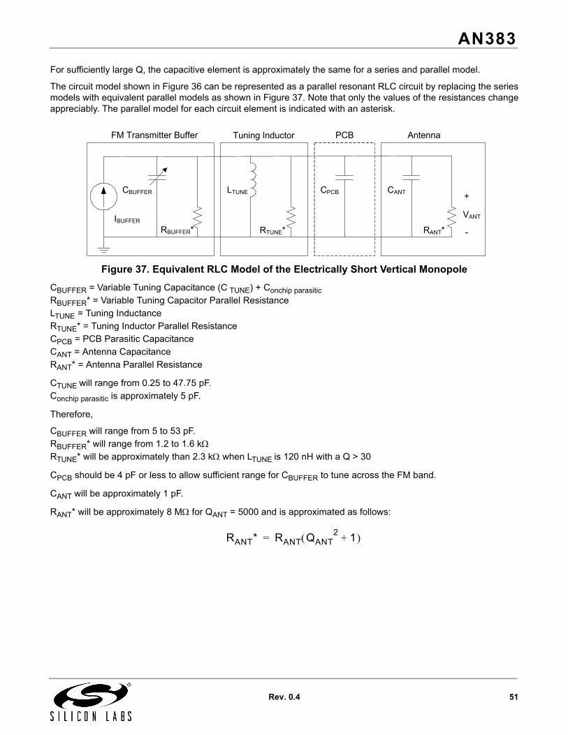
AN383
Rev. 0.4 51
For sufficiently large Q, the capacitive element is approximately the same for a series and parallel model.
The circuit model shown in Figure 36 can be represented as a parallel resonant RLC circuit by replacing the seriesmodels with equivalent parallel models as shown in Figure 37. Note that only the values of the resistances changeappreciably. The parallel model for each circuit element is indicated with an asterisk.
Figure 37. Equivalent RLC Model of the Electrically Short Vertical Monopole
CBUFFER = Variable Tuning Capacitance (C TUNE) + Conchip parasiticRBUFFER* = Variable Tuning Capacitor Parallel ResistanceLTUNE = Tuning InductanceRTUNE* = Tuning Inductor Parallel ResistanceCPCB = PCB Parasitic CapacitanceCANT = Antenna CapacitanceRANT* = Antenna Parallel Resistance
CTUNE will range from 0.25 to 47.75 pF.Conchip parasitic is approximately 5 pF.
Therefore,
CBUFFER will range from 5 to 53 pF.RBUFFER* will range from 1.2 to 1.6 kΩ RTUNE* will be approximately than 2.3 kΩ when LTUNE is 120 nH with a Q > 30
CPCB should be 4 pF or less to allow sufficient range for CBUFFER to tune across the FM band.
CANT will be approximately 1 pF.
RANT* will be approximately 8 MΩ for QANT = 5000 and is approximated as follows:
LTUNE
FM Transmitter Buffer PCBTuning Inductor
RBUFFER*
CBUFFER
RTUNE*
CPCB
RANT*
CANT
Antenna
IBUFFERVANT
+
-
RANT* RANT QANT2 1+( )=
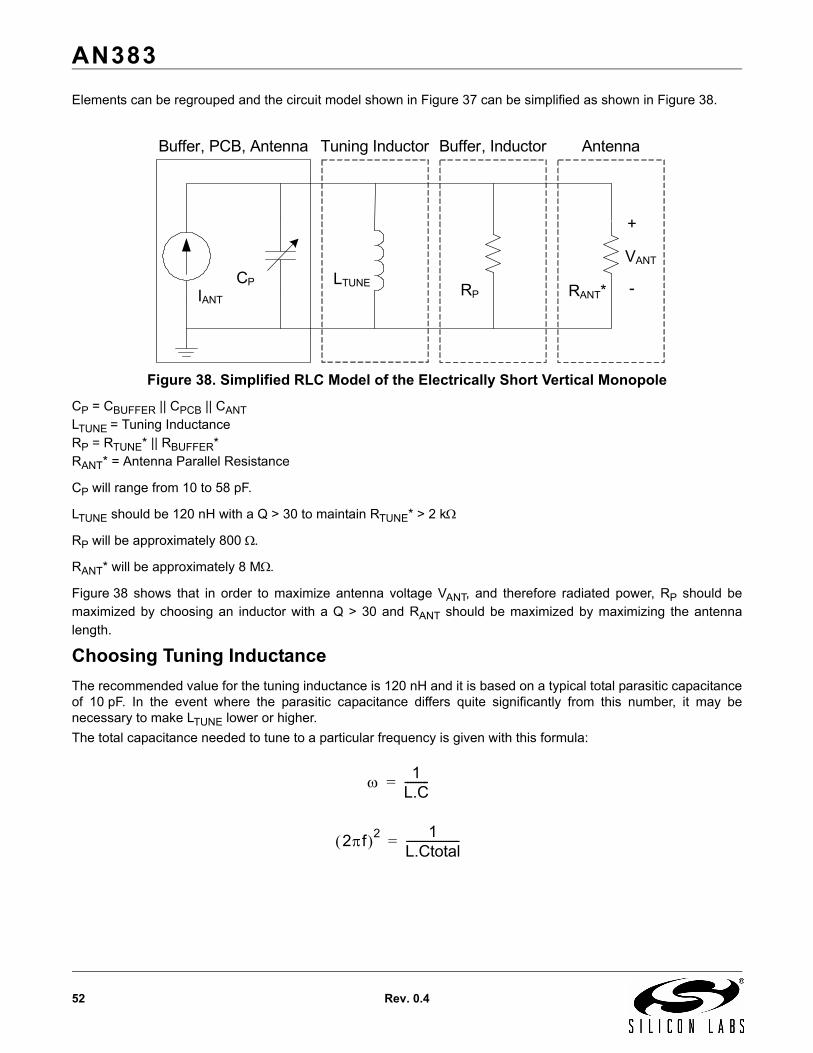
AN383
52 Rev. 0.4
Elements can be regrouped and the circuit model shown in Figure 37 can be simplified as shown in Figure 38.
Figure 38. Simplified RLC Model of the Electrically Short Vertical Monopole
CP = CBUFFER || CPCB || CANTLTUNE = Tuning InductanceRP = RTUNE* || RBUFFER*RANT* = Antenna Parallel Resistance
CP will range from 10 to 58 pF.
LTUNE should be 120 nH with a Q > 30 to maintain RTUNE* > 2 kΩ
RP will be approximately 800 Ω.
RANT* will be approximately 8 MΩ.
Figure 38 shows that in order to maximize antenna voltage VANT, and therefore radiated power, RP should bemaximized by choosing an inductor with a Q > 30 and RANT should be maximized by maximizing the antennalength.
Choosing Tuning InductanceThe recommended value for the tuning inductance is 120 nH and it is based on a typical total parasitic capacitanceof 10 pF. In the event where the parasitic capacitance differs quite significantly from this number, it may benecessary to make LTUNE lower or higher. The total capacitance needed to tune to a particular frequency is given with this formula:
LTUNE
Buffer, PCB, Antenna Buffer, InductorTuning Inductor
CPRANT*
Antenna
RPIANT
VANT
+
-
ω 1L.C---------=
2πf( )2 1L.Ctotal--------------------=
AN383
Rev. 0.4 53
Actual CTUNE needed on the chip then can be calculated by subtracting all of the parasitic capacitance includingthe Si471x on chip parasitic capacitance, PCB capacitance and antenna capacitance.CTUNE = Ctotal – Conchip parasitic – CPCB – CANTThe actual CTUNE needed then has to be well within the available range of CTUNE, which is:CTUNE min = 0.25 pFCTUNE max = 47.75 pFCTUNE can be read from the chip and the range will be 1–191. Each number represents 0.25 pF, so the range is0.25 to 47.75 pF.
Example 1Conchip parasitic = 5 pFCPCB = 4 pFCANT = 1 pFCtotal parasitic capacitance = 5 + 4 + 1 = 10 pFLTUNE = 120 nHDesired FM frequency = 76–108 MHzAt 76 MHz > Ctotal = 37 pF, CTUNE = 37 – 10 = 27 pFAt 108 MHz > Ctotal = 18 pF, CTUNE = 18 – 10 = 8 pFIn this case at the FM frequency of interest (76 MHz to 108 MHz), the needed CTUNE range (8–27 pF) is within theavailable CTUNE range on the chip (0.25–47.75 pF) which means that the 120 nH inductor value is a good choice.
Example 2Conchip parasitic = 5 pFCPCB = 10 pFCANT = 1 pFCtotal parasitic capacitance = 5 + 10 + 1 = 16 pFAt 76 MHz > Ctotal = 37 pF, CTUNE = 37 – 16 = 21 pFAt 108 MHz > Ctotal = 18 pF, CTUNE = 18 – 16 = 2 pFIn this case at 108 MHz even though CTUNE needed (2 pF) is still higher than the min CTUNE (0.25 pF), it is notadvisable to keep LTUNE at 120 nH. Variation in the parasitic capacitance from the PCB and different componentsmay result in the CTUNE needed to be equal or less than 0.25 pF. It is advisable then to lower the LTUNE value to100 nH.
SolutionMake LTUNE = 100 nHAt 76 MHz > Ctotal = 44 pF, CTUNE = 28 pFAt 108 MHz > Ctotal = 22 pF, CTUNE = 6 pFIn this case the needed CTUNE range (6–28 pF) is well within the available CTUNE (0.25 to 47.75 pF).
AN383
54 Rev. 0.4
APPENDIX C—AM FERRITE LOOP STICK ANTENNA INTERFACE MODEL
This appendix describes how to interface a ferrite loop stick antenna to the AM receiver input. The application notebegins with an overview of AM ferrite loop antennas followed by the interface to a ferrite loop stick antenna. Thelast section of the application note presents designers with guidelines for designing ferrite loop stick antennas.
AM Ferrite Loop Stick Antenna OverviewAn AM antenna works on the basis of Faraday's Law. Faraday's law dictates that a varying magnetic field througha wire loop induces an EMF (Electro-Motive Force) in the loop and is expressed as:
Where φ = magnetic flux.The negative sign in Equation indicates that the current generated in the loop is in a direction which generates amagnetic field that opposes the magnetic field causing the induced EMF. An AM loop antenna is made of a singleloop or many loops of a conducting material wrapped around an air core or a ferrite core. In the case of radiotransmissions, the induced voltage represents the AM signal being transmitted by a radio station aselectromagnetic waves.A ferrite loop stick antenna is a coil wrapped around a ferrite core. Ferrite is a ferromagnetic material which doesnot display any magnetic properties till it is excited by a magnetic field. A ferrite multiplies the applied magnetic fieldby a factor that is known as the effective permeability of the ferrite material. Since the permeability of a ferritematerial is orders of magnitude higher than air, the voltage induced in a loop antenna wound around a ferrite coreis also orders of magnitude greater than the voltage that would be induced in an air loop antenna of the same size.All ferrite loop stick antennas have an inductance associated with them and this can be expressed as:
Equation 3. Trap Frequency CalculationWhere:Lant = Antenna inductancek = Permeability modifier constantµr = Relative permeability of ferrite rodµo = Permeability of air/free spaceN = Number of turns in coilA = Cross-sectional area of ferrite rodlr = Length of ferrite rod
In Equation 3, µr is the relative permeability of the ferrite rod. The rod dimensions play an important role indetermining the relative permeability of the rod. The permeability modifier constant is based on the ratio of ferriterod length to the coil length. The relative permeability of the rod and the permeability modifier constant arecombined together to yield the effective permeability of the antenna and are used to reduce Equation 3 to thefollowing:
EMF dϕdt-------–=
LantkμrμoN2A
lr--------------------------=
AN383
Rev. 0.4 55
Equation 4. Ferrite Loop Inductance CalculationWhere µe = Effective relative permeability of antenna
Signal receiving capability of an antenna is defined by its antenna height. Antenna height of a loop antenna isderived from Equation by replacing the flux with the inner product of the magnetic field and the surface area of thecoil and is expressed as follows:
Equation 5. Simplified Ferrite Loop Inductance CalculationWhere:he = Effective antenna heightN = Number of turns in coilA = Cross-sectional area of ferrite rodµe = Relative effective permeability of antennaλ = Wavelength of signal
Equation 6 is used to rewrite the antenna height in terms of antenna inductance as follows:
Equation 6. Effective Antenna Height CalculationWhere:f = Signal frequencyLant = Antenna inductancelr = Length of ferrite rodc = speed of lightµo = Permeability of air/free spaceN = Number of turns in coil
Equation 6 tells us the relationship between antenna height and the factors that affect antenna height. The inducedvoltage can be calculated simply by multiplying the antenna height with the electric field strength for an AM signal(denoted by E) with dimensions of Volts/unit length. Equation 7 expresses this relationship:
Equation 7. Induced Voltage Calculation
LμoμeN2A
Ir------------------------=
he2πNAμe
λ----------------------=
he2πfLantlr
cμoN-----------------------=
Vinduced E2πfLantlr
cμoN-----------------------×=
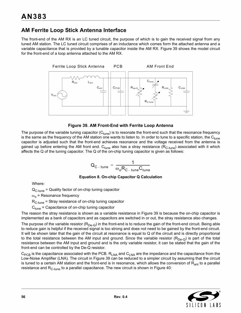
AN383
56 Rev. 0.4
AM Ferrite Loop Stick Antenna InterfaceThe front-end of the AM RX is an LC tuned circuit, the purpose of which is to gain the received signal from anytuned AM station. The LC tuned circuit comprises of an inductance which comes form the attached antenna and avariable capacitance that is provided by a tunable capacitor inside the AM RX. Figure 39 shows the model circuitfor the front-end of a loop antenna attached to the AM RX.
Figure 39. AM Front-End with Ferrite Loop AntennaThe purpose of the variable tuning capacitor (Ctune) is to resonate the front-end such that the resonance frequencyis the same as the frequency of the AM station one wants to listen to. In order to tune to a specific station, the Ctunecapacitor is adjusted such that the front-end achieves resonance and the voltage received from the antenna isgained up before entering the AM front end. Ctune also has a stray resistance (RC-tune) associated with it whichaffects the Q of the tuning capacitor. The Q of the on-chip tuning capacitor is given as follows:
Equation 8. On-chip Capacitor Q CalculationWhere:QC-tune = Quality factor of on-chip tuning capacitorωo = Resonance frequencyRC-tune = Stray resistance of on-chip tuning capacitorCtune = Capacitance of on-chip tuning capacitor
The reason the stray resistance is shown as a variable resistance in Figure 39 is because the on-chip capacitor isimplemented as a bank of capacitors and as capacitors are switched in or out, the stray resistance also changes.The purpose of the variable resistor (RDe-Q) in the front-end is to reduce the gain of the front-end circuit. Being ableto reduce gain is helpful if the received signal is too strong and does not need to be gained by the front-end circuit.It will be shown later that the gain of the circuit at resonance is equal to Q of the circuit and is directly proportionalto the total resistance between the AM input and ground. Since the variable resistor (RDe-Q) is part of the totalresistance between the AM input and ground and is the only variable resistor, it can be stated that the gain of thefront-end can be controlled by the De-Q resistor.CPCB is the capacitance associated with the PCB. RLNA and CLNA are the impedance and the capacitance from theLow-Noise Amplifier (LNA). The circuit in Figure 39 can be reduced to a simpler circuit by assuming that the circuitis tuned to a certain AM station and the front-end is in resonance, which allows the conversion of Rant to a parallelresistance and RC-tune to a parallel capacitance. The new circuit is shown in Figure 40:
PCB AM Front End
Vant
LantRant
CPCB Rde-Q
Ctune
CLNARLNA
Ferrite Loop Stick Antenna
RC-tune
Cant
QC tune–1
ωoRC tune– Ctune-------------------------------------------=
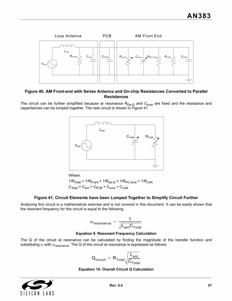
AN383
Rev. 0.4 57
Figure 40. AM Front-end with Series Antenna and On-chip Resistances Converted to Parallel Resistances
The circuit can be further simplified because at resonance RDe-Q and Ctune are fixed and the resistance andcapacitances can be lumped together. The new circuit is shown in Figure 41.
Figure 41. Circuit Elements have been Lumped Together to Simplify Circuit FurtherAnalyzing this circuit is a mathematical exercise and is not covered in this document. It can be easily shown thatthe resonant frequency for this circuit is equal to the following:
Equation 9. Resonant Frequency CalculationThe Q of the circuit at resonance can be calculated by finding the magnitude of the transfer function andsubstituting ω with ωresonance. The Q of the circuit at resonance is expressed as follows:
Equation 10. Overall Circuit Q Calculation
PCB AM Front End
Vant
RP-ant CPCB Rde-Q Ctune CLNARLNA
Loop Antenna
RPC-tune
Lant
Cant
Where:1/RTotal = 1/RP-ant + 1/Rde-Q + 1/RPC-tune + 1/RLNACTotal = Cant + CPCB + Ctune + CLNA
CTotal RTotal
Vant
Lant
ωresonance1
LantCTotal
------------------------------=
Qcircuit RTotalLant
CTotal---------------=

AN383
58 Rev. 0.4
DOCUMENT CHANGE LIST
Revision 0.3 to Revision 0.4Updated "2. Si47xx 3x3 mm QFN Schematic and Layout" on page 5 with latest recommendation on schematic, layout and design guidelines.Added "5. Cable Antenna for FM Transmit and Receive (Si4704/05/06/1x/2x Only)" on page 27.Added "6. Whip Antenna for FM/WB Receiver (Si4736/37/38/39 Only)" on page 30.Updated "7. Ferrite Loop Antenna for AM/LW Receive (Si4730/31/34/35/36/37 Only)" on page 32 with ferrite loop antenna pictures, recommendation and vendor information.Updated "8. Air Loop Antenna for AM/LW Receive (Si4730/31/34/35/36/37 Only)" on page 35 with air loop antenna pictures, transformer recommendation and vendor information.Added "9. Whip Antenna for SW Receiver (Si4734/35 Only)" on page 38.
AN383
Rev. 0.4 59
NOTES:
AN383
60 Rev. 0.4
CONTACT INFORMATIONSilicon Laboratories Inc.400 West Cesar ChavezAustin, TX 78701Tel: 1+(512) 416-8500Fax: 1+(512) 416-9669Toll Free: 1+(877) 444-3032Email: [email protected]: www.silabs.com
Silicon Laboratories and Silicon Labs are trademarks of Silicon Laboratories Inc.Other products or brandnames mentioned herein are trademarks or registered trademarks of their respective holders.
The information in this document is believed to be accurate in all respects at the time of publication but is subject to change without notice. Silicon Laboratories assumes no responsibility for errors and omissions, and disclaims responsibility for any consequences resulting from the use of information included herein. Additionally, Silicon Laboratories assumes no responsibility for the functioning of undescribed features or parameters. Silicon Laboratories reserves the right to make changes without further notice. Silicon Laboratories makes no warranty, rep-resentation or guarantee regarding the suitability of its products for any particular purpose, nor does Silicon Laboratories assume any liability arising out of the application or use of any product or circuit, and specifically disclaims any and all liability, including without limitation conse-quential or incidental damages. Silicon Laboratories products are not designed, intended, or authorized for use in applications intended to support or sustain life, or for any other application in which the failure of the Silicon Laboratories product could create a situation where per-sonal injury or death may occur. Should Buyer purchase or use Silicon Laboratories products for any such unintended or unauthorized ap-plication, Buyer shall indemnify and hold Silicon Laboratories harmless against all claims and damages.