dart.ece.ucdavis.edudart.ece.ucdavis.edu/.../team_stark/an_christian_hurd.docx · web viewfigure 1...
TRANSCRIPT
Christian Hurd996715221Stark IndustriesEEC 134B
Applications note for Radar Project
I. Initialize Broadband filter, DAC, and Voltage Regulator PCB design
In this PCB design I started the design but James made later modifications and finished the design. This PCB included the IC Low pass filter (MAX291CSA+), an IC Voltage Gain amplifier (AD8367ARUZ-RL7), a 7 V to 3.3 V voltage regulator (UA78M33CDCYR), a 7V to 5 V voltage regulator (UA78M05CDCYR), 16 bit digital to analog converter(DAC8551IADGKT), and a slide switch (GF-124-0000). The PCB design required the open software Kicad. The first task of the PCB was to set up the circuit schematic of the circuit which can be seen below. From there I had to find complementary footprints for each part that was being placed on the PCB. Once all parts had their own corresponding footprint I then made a PCB layout and made all the connections. The PCB layout can be seen below as well. When completing the gerber files, I sent all files to a team member (James Chen) so he can verify the design and finalize it for fabrication.
Figure 1 - PCB circuit schematic (not finalized schematic)
Figure 2 - PCB layout (not final layout)

II. Test Patch antennas in an Anechoic Chamber
I tested the transmit and receive patch antennas with Meijiao Li in a RF/Microwave anechoic chamber. While conducting tests in the chamber, a horn antenna was being used as the transmit antenna and the patch antenna that was designed and fabricated for 24 GHz was used for the receive. In order to conduct the test a Calibration set for the frequencies of 23-26 GHz was saved to the HP 8510 network analyzer. Then the patch antenna was tied down to the receive end of the chamber which is a rotating mount that is powered by a motor. As the chamber test is conducted the mount does a 180 degree sweep from -90 to 90 degrees and the network analyzer does a frequency sweep between 23-26 GHz. The output port of the 8510 sends the collected S21, Power collected by receive antenna/Power available from transmit antenna, in dB scale to the computer where the data can be saved for processing. The S21 data was then used in the Friis transmission equation to calculate the gain of the 24 GHz patch

antenna vs antenna rotation angle (theta). The Friis transmission equation goes as followed:
RAB = 11 ft = 3.3528 m10*log10(Pr/Pt) = S21GA-db = gain of transmit antenna = ~20 dBiλ = 0.0125 mBelow are pictures of the 24 GHz patch antenna (figure 3), the anechoic chamber test set-up (figure 4), and the plot of Gain (dB) vs antenna rotation angle (theta) (figure 5)
figure 3 - 24 GHz patch antenna
figure 4 - Transmit antenna, HP 8510 network analyzer, and anechoic chamber

figure 6 - Gain (dB) of 24 GHz patch antenna vs Theta
III. Design and wire active LPF

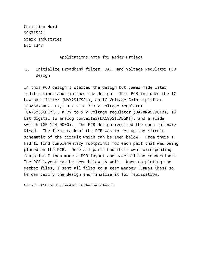
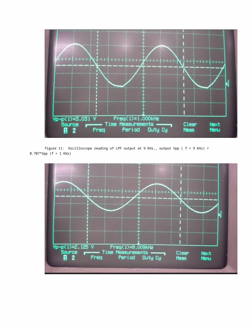
Due the amount of noise attributed from the surface mount IC LPF on the PCB, I had to design our own “off chip” LPF. The LPF was designed and fabricated using a breadboard and lumped elements. The LPF design was featured off the active LPF from the first quarter and had a cutoff frequency of about 9 KHz. To test the LPF I had to connect a 100 mV sine wave that swept from 1 KHz to to about 10 KHz. At 1 KHz the peak to peak output voltage (Vpp) on the oscilloscope was roughly 3 Vpp (figure 10). When increasing frequency I noticed that Vpp decreased and when the Vpp was 0.707*Vpp (2.121 V) then I marked the cutoff frequency which was about 9 KHz (figure 11).Below are images of both the drawn circuit schematic and a picture of the circuit after it was built.
figure 7 - LPF circuit schematic
figure 8 - LPF wired on breadboard
figure 10: Oscilloscope reading of LPF output at 1 KHz and input Vpp = 100 mV

figure 11: Oscilloscope reading of LPF output at 9 KHz,, output Vpp ( f = 9 KHz) = 0.707*Vpp (f = 1 KHz)
IV. Connect entire radar system and test

In this step I set up the entire system and tested the radar. Below is a checklist tasks to assemble the system for both doppler and range radar:
Doppler:
● Power up the PCB that holds the Rx/Tx antennas and the infineon transceiver with 3.3 V
● Power up the PCB that has the (7V to 3.3V) voltage regulator with 7 V and connect 3.3 V feed to the Vcc pin on infineon
● Power up the active LPF with 5 V Vcc and 9V to power the Texas Instrument OPA4228 quad Op-Amp chip
● Power fine and coarse pins on infineon with 2.25 V● Power ardurino with 5V and connect it to infineon PCB at the SPI pin, ardurino has the
SPI code that controls the power amplifier on the infineon● Connect IF output to the input of the active LPF● Analyze output signal of active LPF either on oscilloscope or on audacity software. If on
audacity software, save WAV file and process the file on Matlab for image
video 1: test run of Doppler radarDoppler radar test runhttps://www.youtube.com/watch?v=aib-R-qedRk
Range:
● Power up the PCB that holds the Rx/Tx antennas and the infineon transceiver with 3.3 V
● Power up the PCB that has the (7V to 3.3V) voltage regulator with 7 V and connect 3.3 V feed to the Vcc pin on infineon
● Power up the active LPF with 5 V Vcc and 9V to power the Texas Instrument OPA4228 quad Op-Amp chip
● Power up VCO PCB with 7 V. Triangle wave output will connect to both fine and coarse pins of the infineon and square wave output will connect to the SPI wire that feeds into cable that leads into laptop where the audacity software is ran
● Power ardurino with 5V and connect it to infineon PCB at the SPI pin, ardurino has the SPI code that controls the power amplifier on the infineon
● Connect IF output to the input of the active LPF● Analyze output signal of active LPF either on oscilloscope or on audacity software. If on
audacity software, save WAV file and process the file on Matlab for image
video 2: range radar run
Range Radar test experiementhttps://www.youtube.com/watch?v=sf9HqxTfP9A
Range Radar oscilloscope resultshttps://www.youtube.com/watch?v=CI3yRfpXzIQ