xilinx ug356 ml510 embedded development platform, user guide · ml510 embedded development platform...
TRANSCRIPT

R
ML510 Embedded Development User Guide [optional]
UG356 (v1.2) June 16, 2011 [optional]
ML510 Embedded Development PlatformUser Guide
UG356 (v1.2) June 16, 2011

ML510 Embedded Development Platform www.xilinx.com UG356 (v1.2) June 16, 2011
© Copyright 2008 – 2011 Xilinx, Inc. Xilinx, the Xilinx logo, Artix, ISE, Kintex, Spartan, Virtex, Zynq, and other designated brands included herein are trademarks of Xilinx in the United States and other countries. All other trademarks are the property of their respective owners.
DISCLAIMER
The information disclosed to you hereunder (the “Materials”) is provided solely for the selection and use of Xilinx products. To the maximum extent permitted by applicable law: (1) Materials are made available "AS IS" and with all faults, Xilinx hereby DISCLAIMS ALL WARRANTIES AND CONDITIONS, EXPRESS, IMPLIED, OR STATUTORY, INCLUDING BUT NOT LIMITED TO WARRANTIES OF MERCHANTABILITY, NON-INFRINGEMENT, OR FITNESS FOR ANY PARTICULAR PURPOSE; and (2) Xilinx shall not be liable (whether in contract or tort, including negligence, or under any other theory of liability) for any loss or damage of any kind or nature related to, arising under, or in connection with, the Materials (including your use of the Materials), including for any direct, indirect, special, incidental, or consequential loss or damage (including loss of data, profits, goodwill, or any type of loss or damage suffered as a result of any action brought by a third party) even if such damage or loss was reasonably foreseeable or Xilinx had been advised of the possibility of the same. Xilinx assumes no obligation to correct any errors contained in the Materials, or to advise you of any corrections or update. You may not reproduce, modify, distribute, or publicly display the Materials without prior written consent. Certain products are subject to the terms and conditions of the Limited Warranties which can be viewed at http://www.xilinx.com/warranty.htm; IP cores may be subject to warranty and support terms contained in a license issued to you by Xilinx. Xilinx products are not designed or intended to be fail-safe or for use in any application requiring fail-safe performance; you assume sole risk and liability for use of Xilinx products in Critical Applications: http://www.xilinx.com/warranty.htm#critapps.
Revision History
The following table shows the revision history for this document.
Date Version Revision
08/25/08 1.0 Initial Xilinx release.
08/29/08 1.0.1 Minor typographical edits.
12/11/08 1.1• Added “System Monitor” section.• Corrected Table 1-40, page 71, pins A15 and A16.• Removed support for unbuffered DIMMs.
06/16/11 1.2 Corrected FPGA pin “H7” to pin ”J15” in section “CPU Reset (SW2),” page 58.
R
ML510 Embedded Development Platform www.xilinx.com 3UG356 (v1.2) June 16, 2011
Preface: About This GuideAdditional Documentation . . . . . . . . . . . . . . . . . . . . . . . . . . . . . . . . . . . . . . . . . . . . . . . . . . . 5Additional Support Resources . . . . . . . . . . . . . . . . . . . . . . . . . . . . . . . . . . . . . . . . . . . . . . . . 6Typographical Conventions . . . . . . . . . . . . . . . . . . . . . . . . . . . . . . . . . . . . . . . . . . . . . . . . . . 6
Online Document . . . . . . . . . . . . . . . . . . . . . . . . . . . . . . . . . . . . . . . . . . . . . . . . . . . . . . . . . . 6
Chapter 1: ML510 Embedded Development PlatformOverview . . . . . . . . . . . . . . . . . . . . . . . . . . . . . . . . . . . . . . . . . . . . . . . . . . . . . . . . . . . . . . . . . . . . 9
Package Contents . . . . . . . . . . . . . . . . . . . . . . . . . . . . . . . . . . . . . . . . . . . . . . . . . . . . . . . . . . 9Additional Information . . . . . . . . . . . . . . . . . . . . . . . . . . . . . . . . . . . . . . . . . . . . . . . . . . . . 10Features . . . . . . . . . . . . . . . . . . . . . . . . . . . . . . . . . . . . . . . . . . . . . . . . . . . . . . . . . . . . . . . . . 10Block Diagram . . . . . . . . . . . . . . . . . . . . . . . . . . . . . . . . . . . . . . . . . . . . . . . . . . . . . . . . . . . 11
Related Xilinx Documents . . . . . . . . . . . . . . . . . . . . . . . . . . . . . . . . . . . . . . . . . . . . . . . . . . . 11Detailed Description . . . . . . . . . . . . . . . . . . . . . . . . . . . . . . . . . . . . . . . . . . . . . . . . . . . . . . . . 12
Virtex-5 FPGA . . . . . . . . . . . . . . . . . . . . . . . . . . . . . . . . . . . . . . . . . . . . . . . . . . . . . . . . . . . 13Configuration . . . . . . . . . . . . . . . . . . . . . . . . . . . . . . . . . . . . . . . . . . . . . . . . . . . . . . . . . 13I/O Voltage Rails . . . . . . . . . . . . . . . . . . . . . . . . . . . . . . . . . . . . . . . . . . . . . . . . . . . . . . 13
Clock Generation . . . . . . . . . . . . . . . . . . . . . . . . . . . . . . . . . . . . . . . . . . . . . . . . . . . . . . . . . 14DDR2 Memory . . . . . . . . . . . . . . . . . . . . . . . . . . . . . . . . . . . . . . . . . . . . . . . . . . . . . . . . . . . 16
MIG Compliance. . . . . . . . . . . . . . . . . . . . . . . . . . . . . . . . . . . . . . . . . . . . . . . . . . . . . . . 16Dual DDR2 SDRAM DIMMs . . . . . . . . . . . . . . . . . . . . . . . . . . . . . . . . . . . . . . . . . . . . . 17
10/100/1000 Tri-Speed Ethernet PHY . . . . . . . . . . . . . . . . . . . . . . . . . . . . . . . . . . . . . . . 26System ACE and CompactFlash Connector . . . . . . . . . . . . . . . . . . . . . . . . . . . . . . . . . . . 31
Board Bring-Up through the JTAG Interface . . . . . . . . . . . . . . . . . . . . . . . . . . . . . . . . . 32Non-Volatile Storage through the MPU Interface. . . . . . . . . . . . . . . . . . . . . . . . . . . . . . 33
Linear Flash Memory . . . . . . . . . . . . . . . . . . . . . . . . . . . . . . . . . . . . . . . . . . . . . . . . . . . . . 34GPIO LEDs and LCD . . . . . . . . . . . . . . . . . . . . . . . . . . . . . . . . . . . . . . . . . . . . . . . . . . . . . . 37
GPIO LED Interface . . . . . . . . . . . . . . . . . . . . . . . . . . . . . . . . . . . . . . . . . . . . . . . . . . . . 38GPIO LCD Interface . . . . . . . . . . . . . . . . . . . . . . . . . . . . . . . . . . . . . . . . . . . . . . . . . . . . 38
JTAG Trace/Debug . . . . . . . . . . . . . . . . . . . . . . . . . . . . . . . . . . . . . . . . . . . . . . . . . . . . . . . 39CPU Debug Description . . . . . . . . . . . . . . . . . . . . . . . . . . . . . . . . . . . . . . . . . . . . . . . . . 39CPU JTAG Header Pinout . . . . . . . . . . . . . . . . . . . . . . . . . . . . . . . . . . . . . . . . . . . . . . . 42CPU JTAG Connection to FPGA. . . . . . . . . . . . . . . . . . . . . . . . . . . . . . . . . . . . . . . . . . . 42
DVI Output . . . . . . . . . . . . . . . . . . . . . . . . . . . . . . . . . . . . . . . . . . . . . . . . . . . . . . . . . . . . . . 42PCI Express Interface . . . . . . . . . . . . . . . . . . . . . . . . . . . . . . . . . . . . . . . . . . . . . . . . . . . . . . 43PCI Bus . . . . . . . . . . . . . . . . . . . . . . . . . . . . . . . . . . . . . . . . . . . . . . . . . . . . . . . . . . . . . . . . . 46ALi South Bridge Interface, M1535D+ (U15) . . . . . . . . . . . . . . . . . . . . . . . . . . . . . . . . . . 49
USB Connector Assembly (J3). . . . . . . . . . . . . . . . . . . . . . . . . . . . . . . . . . . . . . . . . . . . . 50IDE Connectors (J15 and J16) . . . . . . . . . . . . . . . . . . . . . . . . . . . . . . . . . . . . . . . . . . . . . 50System Management Bus Controller. . . . . . . . . . . . . . . . . . . . . . . . . . . . . . . . . . . . . . . . 51AC’97 Audio Interface . . . . . . . . . . . . . . . . . . . . . . . . . . . . . . . . . . . . . . . . . . . . . . . . . . 52PS/2 Keyboard and Mouse Interface Connector (P2) . . . . . . . . . . . . . . . . . . . . . . . . . . . 52
IIC/SMBus Interface . . . . . . . . . . . . . . . . . . . . . . . . . . . . . . . . . . . . . . . . . . . . . . . . . . . . . . 53Introduction to IIC/SMBus. . . . . . . . . . . . . . . . . . . . . . . . . . . . . . . . . . . . . . . . . . . . . . . 53IIC/SMBus Signaling . . . . . . . . . . . . . . . . . . . . . . . . . . . . . . . . . . . . . . . . . . . . . . . . . . . 53IIC/SMBus . . . . . . . . . . . . . . . . . . . . . . . . . . . . . . . . . . . . . . . . . . . . . . . . . . . . . . . . . . . 53
Table of Contents
4 www.xilinx.com ML510 Embedded Development PlatformUG356 (v1.2) June 16, 2011
R
Serial Peripheral Interface . . . . . . . . . . . . . . . . . . . . . . . . . . . . . . . . . . . . . . . . . . . . . . . . . . 55SPI Signaling. . . . . . . . . . . . . . . . . . . . . . . . . . . . . . . . . . . . . . . . . . . . . . . . . . . . . . . . . . 55SPI Addressing . . . . . . . . . . . . . . . . . . . . . . . . . . . . . . . . . . . . . . . . . . . . . . . . . . . . . . . . 56
Serial ATA . . . . . . . . . . . . . . . . . . . . . . . . . . . . . . . . . . . . . . . . . . . . . . . . . . . . . . . . . . . . . . . 56Serial ATA Description . . . . . . . . . . . . . . . . . . . . . . . . . . . . . . . . . . . . . . . . . . . . . . . . . . 56FPGA to Serial ATA Connector . . . . . . . . . . . . . . . . . . . . . . . . . . . . . . . . . . . . . . . . . . . 57
Pushbuttons, Switches, Front Panel Interface, and Jumpers . . . . . . . . . . . . . . . . . . . . . 57Pushbuttons . . . . . . . . . . . . . . . . . . . . . . . . . . . . . . . . . . . . . . . . . . . . . . . . . . . . . . . . . . 57Switches . . . . . . . . . . . . . . . . . . . . . . . . . . . . . . . . . . . . . . . . . . . . . . . . . . . . . . . . . . . . . 58Front Panel Interface (J23). . . . . . . . . . . . . . . . . . . . . . . . . . . . . . . . . . . . . . . . . . . . . . . . 58Jumpers. . . . . . . . . . . . . . . . . . . . . . . . . . . . . . . . . . . . . . . . . . . . . . . . . . . . . . . . . . . . . . 60
ATX Power Distribution and Voltage Regulation . . . . . . . . . . . . . . . . . . . . . . . . . . . . . 62System Monitor . . . . . . . . . . . . . . . . . . . . . . . . . . . . . . . . . . . . . . . . . . . . . . . . . . . . . . . . . . 64
High-Speed I/O . . . . . . . . . . . . . . . . . . . . . . . . . . . . . . . . . . . . . . . . . . . . . . . . . . . . . . . . . . . . . 66Personality Module Connectors. . . . . . . . . . . . . . . . . . . . . . . . . . . . . . . . . . . . . . . . . . . . . 67
Z-Dok+ Connector Offsets . . . . . . . . . . . . . . . . . . . . . . . . . . . . . . . . . . . . . . . . . . . . . . . 68PM1 Connector . . . . . . . . . . . . . . . . . . . . . . . . . . . . . . . . . . . . . . . . . . . . . . . . . . . . . . . . 69PM2 Connector . . . . . . . . . . . . . . . . . . . . . . . . . . . . . . . . . . . . . . . . . . . . . . . . . . . . . . . . 69Adapter Board PM Connectors. . . . . . . . . . . . . . . . . . . . . . . . . . . . . . . . . . . . . . . . . . . . 69
Z-DOK+ Utility Pins . . . . . . . . . . . . . . . . . . . . . . . . . . . . . . . . . . . . . . . . . . . . . . . . . . . . . . 70Contact Order . . . . . . . . . . . . . . . . . . . . . . . . . . . . . . . . . . . . . . . . . . . . . . . . . . . . . . . . . 70PM1 Power and Ground . . . . . . . . . . . . . . . . . . . . . . . . . . . . . . . . . . . . . . . . . . . . . . . . . 71
PM User I/O Pins. . . . . . . . . . . . . . . . . . . . . . . . . . . . . . . . . . . . . . . . . . . . . . . . . . . . . . . . . 71PM1 User I/O . . . . . . . . . . . . . . . . . . . . . . . . . . . . . . . . . . . . . . . . . . . . . . . . . . . . . . . . . 71PM2 User I/O . . . . . . . . . . . . . . . . . . . . . . . . . . . . . . . . . . . . . . . . . . . . . . . . . . . . . . . . . 74
Configuration Options . . . . . . . . . . . . . . . . . . . . . . . . . . . . . . . . . . . . . . . . . . . . . . . . . . . . . . 77JTAG (Xilinx Download Cable and System ACE Controller) Configuration . . . . . . . 77System ACE Controller Configuration . . . . . . . . . . . . . . . . . . . . . . . . . . . . . . . . . . . . . . . 78Linear Flash Memory Configuration . . . . . . . . . . . . . . . . . . . . . . . . . . . . . . . . . . . . . . . . 79
Appendix A: References

ML510 Embedded Development Platform www.xilinx.com 5UG356 (v1.2) June 16, 2011
R
Preface
About This Guide
This manual accompanies the ML510 series of Embedded Development Platforms and contains information about the ML510 hardware and software tools.
Guide ContentsThis manual contains the following chapters:
• Chapter 1, “ML510 Embedded Development Platform” provides an overview of the embedded development platform and details the components and features of the ML510 board
• Appendix A, “References”
Additional DocumentationThe following documents are also available for download at http://www.xilinx.com/virtex5.
• Virtex-5 Family Overview
The features and product selection of the Virtex-5 family are outlined in this overview.
• Virtex-5 FPGA Data Sheet: DC and Switching Characteristics
This data sheet contains the DC and Switching Characteristic specifications for the Virtex-5 family.
• Virtex-5 FPGA Integrated Endpoint Block User Guide for PCI Express Designs
This guide describes the integrated Endpoint blocks in the Virtex-5 LXT and SXT platform devices that are PCI Express® compliant.
• Virtex-5 FPGA User Guide
Chapters in this guide cover the following topics: Clocking resources, Clock Management Technology (CMT), Phase-Locked Loops (PLLs), block RAM, Configurable Logic Blocks (CLBs), SelectIO™ resources, and SelectIO logic resources
• Virtex-5 FPGA RocketIO™ GTX Transceiver User Guide
This guide describes the RocketIO GTX transceivers available in the Virtex-5 FXT platform devices.
• Virtex-5 FPGA Embedded Tri-Mode Ethernet MAC
This guide describes the dedicated Tri-Mode Ethernet Media Access Controller available in the Virtex-5 LXT, SXT, and FXT platform devices.

6 www.xilinx.com ML510 Embedded Development PlatformUG356 (v1.2) June 16, 2011
Preface: About This GuideR
• XtremeDSP Design Considerations
This guide describes the XtremeDSP™ slice and includes reference designs for using the DSP48E.
• Virtex-5 FPGA Configuration Guide
This all-encompassing configuration guide includes chapters on configuration interfaces (serial and SelectMAP), bitstream encryption, Boundary-Scan and JTAG configuration, reconfiguration techniques, and readback through the SelectMAP and JTAG interfaces.
• Virtex-5 FPGA System Monitor User Guide
The System Monitor functionality available in all the Virtex-5 devices is outlined in this guide.
• Virtex-5 FPGA Packaging Specifications
This specification includes the tables for device/package combinations and maximum I/Os, pin definitions, pinout tables, pinout diagrams, mechanical drawings, and thermal specifications.
• Virtex-5 FPGA PCB Designer’s Guide
This guide provides information on PCB design for Virtex-5 devices, with a focus on strategies for making design decisions at the PCB and interface level.
Additional Support ResourcesTo search the database of silicon and software questions and answers, or to create a technical support case in WebCase, see the Xilinx website at:http://www.xilinx.com/support.
Typographical ConventionsThis document uses the following typographical conventions. An example illustrates each convention.
Online DocumentThe following conventions are used in this document:
Convention Meaning or Use Example
Italic font
References to other documentsSee the Virtex-5 Configuration Guide for more information.
Emphasis in textThe address (F) is asserted after clock event 2.
Underlined Text Indicates a link to a web page. http://www.xilinx.com/virtex5
Convention Meaning or Use Example
Blue textCross-reference link to a location in the current document
See the section “Additional Documentation” for details.

ML510 Embedded Development Platform www.xilinx.com 7UG356 (v1.2) June 16, 2011
Typographical ConventionsR
Red textCross-reference link to a location in another document
See Figure 5 in the Virtex-5 Data Sheet
Blue, underlined text Hyperlink to a website (URL)Go to http://www.xilinx.com for the latest documentation.
Convention Meaning or Use Example

8 www.xilinx.com ML510 Embedded Development PlatformUG356 (v1.2) June 16, 2011
Preface: About This GuideR
ML510 Embedded Development Platform www.xilinx.com 9UG356 (v1.2) June 16, 2011
R
Chapter 1
ML510 Embedded Development Platform
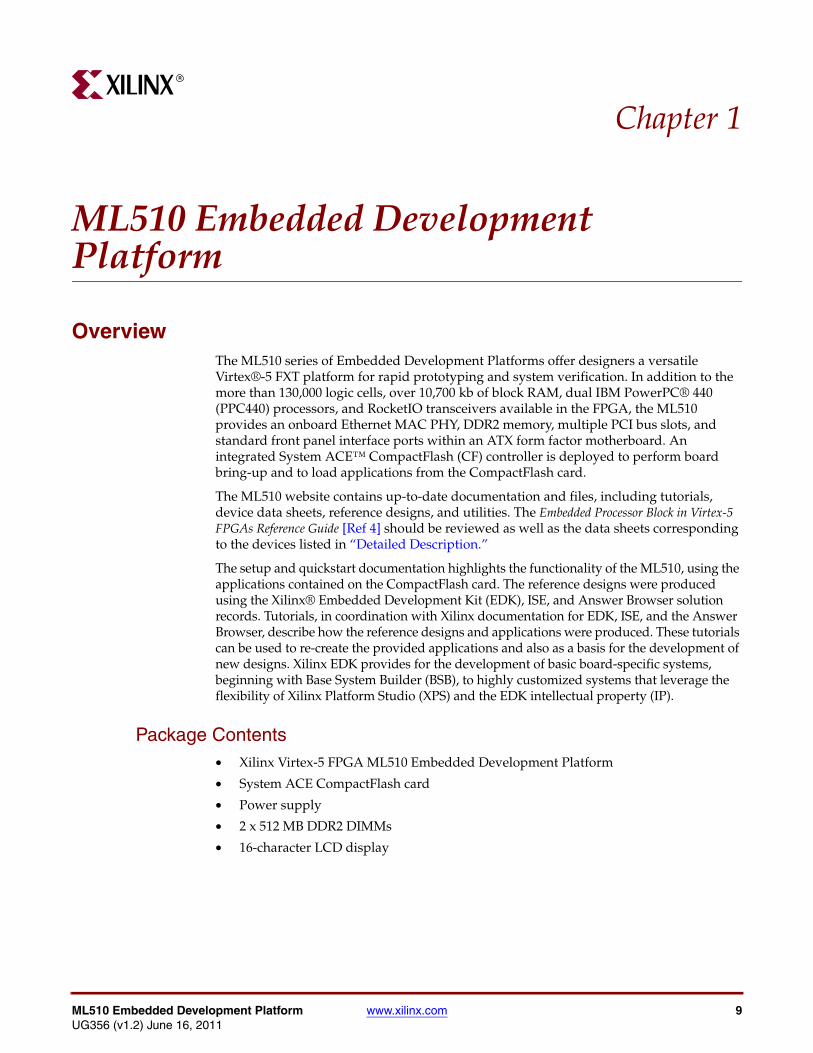
OverviewThe ML510 series of Embedded Development Platforms offer designers a versatile Virtex®-5 FXT platform for rapid prototyping and system verification. In addition to the more than 130,000 logic cells, over 10,700 kb of block RAM, dual IBM PowerPC® 440 (PPC440) processors, and RocketIO transceivers available in the FPGA, the ML510 provides an onboard Ethernet MAC PHY, DDR2 memory, multiple PCI bus slots, and standard front panel interface ports within an ATX form factor motherboard. An integrated System ACE™ CompactFlash (CF) controller is deployed to perform board bring-up and to load applications from the CompactFlash card.
The ML510 website contains up-to-date documentation and files, including tutorials, device data sheets, reference designs, and utilities. The Embedded Processor Block in Virtex-5 FPGAs Reference Guide [Ref 4] should be reviewed as well as the data sheets corresponding to the devices listed in “Detailed Description.”
The setup and quickstart documentation highlights the functionality of the ML510, using the applications contained on the CompactFlash card. The reference designs were produced using the Xilinx® Embedded Development Kit (EDK), ISE, and Answer Browser solution records. Tutorials, in coordination with Xilinx documentation for EDK, ISE, and the Answer Browser, describe how the reference designs and applications were produced. These tutorials can be used to re-create the provided applications and also as a basis for the development of new designs. Xilinx EDK provides for the development of basic board-specific systems, beginning with Base System Builder (BSB), to highly customized systems that leverage the flexibility of Xilinx Platform Studio (XPS) and the EDK intellectual property (IP).
Package Contents• Xilinx Virtex-5 FPGA ML510 Embedded Development Platform
• System ACE CompactFlash card
• Power supply
• 2 x 512 MB DDR2 DIMMs
• 16-character LCD display

10 www.xilinx.com ML510 Embedded Development PlatformUG356 (v1.2) June 16, 2011
Chapter 1: ML510 Embedded Development PlatformR
Additional InformationAdditional information and support material is located at:
• http://www.xilinx.com/ml510
This information includes:
• Current version of this user guide in PDF format
• Example design files for demonstration of Virtex-5 FPGA features and technology
• Demonstration hardware and software configuration files for the System ACE controller, Platform Flash configuration storage device, CPLD, and linear flash chips
• EDK reference design files
• Full schematics in PDF format and ViewDraw schematic format
• PC board layout in Allegro PCB format
• Gerber files for the PC board (Many free or shareware Gerber file viewers are available on the internet for viewing and printing these files.)
• Additional documentation, errata, frequently asked questions, and the latest news
For information about the Virtex-5 family of FPGA devices, including product highlights, data sheets, user guides, and application notes, see the Virtex-5 FPGA website at www.xilinx.com/virtex5. Additional information is available from the data sheets and application notes from the component manufacturers.
Features• ATX form factor motherboard and ATX-compliant power supply
• Dual DDR2 registered DIMMs; each 512 MB density and 72 bits wide
• 512 MB CompactFlash (CF) card and System ACE CF controller for configuration*
• Intel P30 StrataFlash linear flash chip (256 Mb)
• Two onboard 10/100/1000 Ethernet PHYs with RJ-45 connectors
• PCI Express interface and MIC2592B PCI Express power controller
• Two UARTs with RS-232 connectors
• DVI graphics interface
• LEDs, LCD*, and switches
• 32/33 PCI subsystem
♦ Two 3.3V slot and two 5V slots
♦ ALi South Bridge SuperIO controller
- PS/2 mouse and keyboard connectors
- 3.5 mm headphone and microphone connectors
- Two USB peripheral ports
• Two serial ATA connectors
• Xilinx Personality Module (XPM) interface for access to:
♦ RocketIO GTX transceivers
♦ SPI4.2
♦ GPIO
♦ Power

ML510 Embedded Development Platform www.xilinx.com 11UG356 (v1.2) June 16, 2011
Related Xilinx DocumentsR
• JTAG and trace debug ports
• High-speed I/O through RocketIO GTX transceivers
• Encryption battery
• Fan controller
• Onboard power regulators for all necessary voltages
• IIC/SMBus interface*
♦ LTC1694 SMBus accelerator
♦ RTC8566 Real Time Clock (RTC)
♦ 64 kb 24LC64 EEPROM
♦ LM87 voltage/temp monitor
♦ Two DDR2 DIMMs with SPD EEPROMs
• SPI EEPROM (64 Kb)*
Note: * Compatible with EDK supported IP and software drivers
Block DiagramFigure 1-1 shows a high-level block diagram of the ML510 and its peripherals.
Related Xilinx DocumentsPrior to using the ML510 Embedded Development Platform, users should be familiar with Xilinx resources. See Appendix A, “References” for direct links to Xilinx documentation. See the following locations for additional documentation on Xilinx tools and solutions:
• EDK: www.xilinx.com/edk
X-Ref Target - Figure 1-1
Figure 1-1: ML510 High-Level Block Diagram
IIC / SMBus
2x RS-232
Parallel Flash
CF System ACE
SPI
GPIO / LEDs
3.3V PCI
5V PCI
3.3V PCISlots
PCI ExpressSlots
PCI-to-PCIBridge
5V PCISlots
FPGA
2x Gbit Ethernet
2x Serial ATA
DDR2 DIMM
High-speed XPM1
High-speed XPM2
DDR2 DIMM
2x USB
2x IDE
SMBus
2x PS/2ALi
M1535D+South Bridge
Audio
DVI
UG356_c1_01_082508

12 www.xilinx.com ML510 Embedded Development PlatformUG356 (v1.2) June 16, 2011
Chapter 1: ML510 Embedded Development PlatformR
• ISE: www.xilinx.com/ise
• Answer Browser: www.xilinx.com/support
• Intellectual Property: www.xilinx.com/ipcenter
Detailed DescriptionThe ML510, shown in Figure 1-2, is an example of the ML510 series described in this user guide.
X-Ref Target - Figure 1-2
Figure 1-2: ML510 Board and Front Panel Detail
System ACE CFController, U38
System OSC and Socket
GTX Differential Clock Connectors, J17
ATX PowerConnector, J18
Front PanelHeader, J23
System ACE Configuration DIP Switch, SW3
System ACE Status and Error LEDs
LCD Interface Header, J13
CPU JTAG Header, J12
Parallel Cable IV (PC4) JTAG, J9
Reset Switches, SW1/SW2
PCI Slots(3.3V and 5.5V)
PCI Express Slots
CompactFlashSlot, J22
IDE Drive Connectors,
J15/J16
PM1 Expansion Slot
GTX Differential Clock, J20/J21
PM2 Expansion Slot
FPGA JTAG/TRACEDebug Connector, P8
Virtex-5XC5VFX130T
FPGA, U37
Power Supply Monitors,LEDs, and Test Points
GPIO Header, J5
CDROM In, J6
Line Out, J2Line In, J2
ALi South BridgeSuper I/O
Controller, U15
PCI-to-PCI Bridge, U32
3.3V PCI
5.0V PCI
3.3V PCI
Serial ATAHost Connectors
5.0V PCI
OSCSocket
LinearFlash, U43
DDR2 DIMMMemories
DVI Port,P10
Ethernet Ports x 2, P7
Prog Pushbutton, SW4
USB A/B, J3
Mic In and Amp Out, J1
PS/2 Mouse, Keyboard, P1
UG356_c1_02_082508
ML510 Embedded Development Platform www.xilinx.com 13UG356 (v1.2) June 16, 2011
Detailed DescriptionR
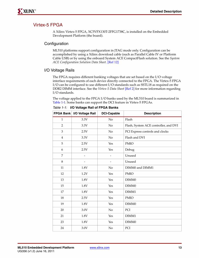
Virtex-5 FPGAA Xilinx Virtex-5 FPGA, XC5VFX130T-2FFG1738C, is installed on the Embedded Development Platform (the board).
Configuration
ML510 platforms support configuration in JTAG mode only. Configuration can be accomplished by using a Xilinx download cable (such as Parallel Cable IV or Platform Cable USB) or by using the onboard System ACE CompactFlash solution. See the System ACE Configuration Solution Data Sheet. [Ref 12]
I/O Voltage Rails
The FPGA requires different banking voltages that are set based on the I/O voltage interface requirements of each device directly connected to the FPGA. The Virtex-5 FPGA I/O can be configured to use different I/O standards such as SSTL18 as required on the DDR2 DIMM interface. See the Virtex-5 Data Sheet [Ref 2] for more information regarding I/O standards.
The voltage applied to the FPGA I/O banks used by the ML510 board is summarized in Table 1-1. Some banks can support the DCI feature in Virtex-5 FPGAs.
Table 1-1: I/O Voltage Rail of FPGA Banks
FPGA Bank I/O Voltage Rail DCI-Capable Description
1 3.3V No Flash
2 3.3V No Flash, System ACE controller, and DVI
3 2.5V No PCI Express controls and clocks
4 3.3V No Flash and DVI
5 2.5V Yes PMIO
6 2.5V Yes Debug
7 - - Unused
8 - - Unused
11 1.8V No DIMM0 and DIMM1
12 1.2V Yes PMIO
13 1.8V Yes DIMM0
15 1.8V Yes DIMM0
17 1.8V Yes DIMM1
18 2.5V Yes PMIO
19 1.8V Yes DIMM0
20 3.0V No PCI
21 1.8V Yes DIMM1
23 1.8V Yes DIMM0
24 3.0V No PCI

14 www.xilinx.com ML510 Embedded Development PlatformUG356 (v1.2) June 16, 2011
Chapter 1: ML510 Embedded Development PlatformR
Clock GenerationML510 boards are equipped with two crystal oscillator sockets (X6 and X10) each wired for standard LVTTL-type oscillators. Both sockets accept half- and full-size oscillators. See the reference design documentation on the ML510 website for examples of how to set up the clocks on ML510 boards.
X6 is populated with a 100 MHz oscillator that provides the system clock. This system clock is typically used to generate multiple other clocks with varying frequencies and phases within the FPGA fabric by using the Virtex-5 DCMs. The FPGA also generates and drives clocks required by the DDR2 DIMM memory and PCI bus interfaces. If required, a second user clock can be brought into the FPGA by installing a second oscillator in the X10 socket.
High-precision clock signals can be supplied to the FPGA using differential clock signals brought in through 50Ω SMA connectors. A single-ended clock can be connected to USER_SMA_CLK_P. Two additional single-ended clocks can be supplied through the XPM connectors. Furthermore, ML510 boards are equipped with several high-precision clocks for driving the high-speed RocketIO transceivers. These clocks can also be used to drive the global clock nets of the FPGA. See the Virtex-5 Data Sheet [Ref 2] for details.
25 2.5V No PHY0 and PMIO
26 3.3V No System ACE controller and DVI
Table 1-1: I/O Voltage Rail of FPGA Banks (Cont’d)
FPGA Bank I/O Voltage Rail DCI-Capable Description

ML510 Embedded Development Platform www.xilinx.com 15UG356 (v1.2) June 16, 2011
Detailed DescriptionR
Figure 1-3 is an example of the clock distribution for the ML510 board. X-Ref Target - Figure 1-3
Figure 1-3: ML510 Clock Distribution
OSCSocket
OSCOpenSocket
OSCSoldered
PCIE_126_P
FX200T FX130T
134
130
126
122
120
124
128
132
PCIE_128_P
PCIE_128_N
116
112
114
GTXDualTile
GTXDualTile
GTXDualTile
GTXDualTile
GTXDualTile
GTXDualTile
GTXDualTile
GTXDualTile
GTXDualTile
GTXDualTile
GTXDualTile
GTXDualTile
GTXDualTile
GTXDualTile
118
RE
FCLK
RE
FCLK
(HCSL)
(LVPECL)
100MHz
100MHz
100MHz25MHz
1:4
1:4
SATA_P
SATA_N
SGMII_P
SGMII_N
RE
FCLK
RE
FCLK
GTXDualTile
GTXDualTile
GTXDualTile
GTXDualTile
GTXDualTile
GTXDualTile
GTXDualTile
GTXDualTile
LVDS_CLK_EXT_P
MGT_SMA_CLK_P
LVDS_CLK_EXT_N
MGT_SMA_CLK_N
RE
FCLK
RE
FCLK
PCIE_126_N
ML510 Virtex-5 FPGA
SysAce_CLK
USER_CLK2
USER_CLK 100 MHz
33 MHz
SMA CLK
GCLK
GCLK
GCLK
GCLKP
N
P
P
P
PCIe Slot B
PCIe Slot A PCIeSlotBGTXs
ICS844021I
ICS85104
ICS85104
ICS87400I
SMA_MGT_CLK
ICS844071I
From PersonalityModule
1x/2x
4x
6x
8x
PCIe SlotAGTXs
1x/2x
4x
PCIe SlotClocks
125MHz
75 or 150MHz
25MHz
250MHz(100MHz)
25MHz
ICS843011
PCIE_122_P
PCIE_122_N
REF
CLK
RE
FCLK
PCIE_132_P
PCIE_132_N
UG356_C1_03_082508
100MHz
16 www.xilinx.com ML510 Embedded Development PlatformUG356 (v1.2) June 16, 2011
Chapter 1: ML510 Embedded Development PlatformR
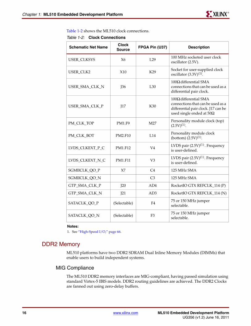
Table 1-2 shows the ML510 clock connections.
DDR2 MemoryML510 platforms have two DDR2 SDRAM Dual Inline Memory Modules (DIMMs) that enable users to build independent systems.
MIG Compliance
The ML510 DDR2 memory interfaces are MIG-compliant, having passed simulation using standard Virtex-5 IBIS models. DDR2 routing guidelines are achieved. The DDR2 Clocks are fanned out using zero-delay buffers.
Table 1-2: Clock Connections
Schematic Net NameClock
SourceFPGA Pin (U37) Description
USER_CLKSYS X6 L29100 MHz socketed user clock oscillator (2.5V).
USER_CLK2 X10 K29Socket for user-supplied clock oscillator (3.3V)(1).
USER_SMA_CLK_N J36 L30100Ω differential SMA connections that can be used as a differential pair clock.
USER_SMA_CLK_P J17 K30
100Ω differential SMA connections that can be used as a differential pair clock. J17 can be used single ended at 50Ω.
PM_CLK_TOP PM1.F9 M27Personality module clock (top) (2.5V)(1).
PM_CLK_BOT PM2.F10 L14Personality module clock (bottom) (2.5V)(1).
LVDS_CLKEXT_P_C PM1.F12 V4LVDS pair (2.5V)(1) . Frequency is user-defined.
LVDS_CLKEXT_N_C PM1.F11 V3LVDS pair (2.5V)(1). Frequency is user-defined.
SGMIICLK_QO_P X7 C4 125 MHz SMA
SGMIICLK_QO_N C3 125 MHz SMA
GTP_SMA_CLK_P J20 AD4 RocketIO GTX REFCLK_114 (P)
GTP_SMA_CLK_N J21 AD3 RocketIO GTX REFCLK_114 (N)
SATACLK_QO_P (Selectable) F4 75 or 150 MHz jumper selectable.
SATACLK_QO_N (Selectable) F3 75 or 150 MHz jumper selectable.
Notes: 1. See “High-Speed I/O,” page 66.
ML510 Embedded Development Platform www.xilinx.com 17UG356 (v1.2) June 16, 2011
Detailed DescriptionR
The board’s DDR2 memory interfaces are designed to the requirements defined by the Xilinx Memory Interface Generator (MIG) User Guide [Ref 21] using the MIG tool [Ref 23]. The MIG documentation requires that designers follow the MIG pinout and layout guidelines. The MIG tool generates and ensures that the proper FPGA I/O pin selections are made in support of the board’s DDR2 interfaces. The initial pin selection for the board was modified and then re-verified to meet the MIG pinout requirements. To ensure a robust interface, the ML510 DDR2 layout incorporates matched trace lengths for data signals to the corresponding data strobe signal as defined in the MIG user guide. See Appendix A, “References” for links to additional information about MIG and Virtex-5 FPGAs in general.
Dual DDR2 SDRAM DIMMs
The DDR2 DIMMs are standard 240-pin DIMM sockets, supporting standard computer DDR2 memory.
ML510 boards are shipped with dual single-rank registered 512 MB PC2-5300 DDR2-667 DIMMs. The DDR2 DIMM is commercially available from Wintec Industries. The DDR2 DIMM uses nine 32M x 8 DDR2 SDRAM devices with 14-row address lines, 10-column address lines, and two bank address lines. Read and write access is programmable in burst lengths of 4 or 8. The memory module inputs and outputs are compatible with SSTL18 signaling. Serial Presence Detect (SPD) using an IIC interface to the DDR DIMM is also supported. See the “IIC/SMBus Interface” section for more details on accessing the DIMM module’s SPD EEPROM.
The DDR2 DIMM memory interface includes a 72-bit wide datapath to the DDR2 DIMM, which includes 8 bits for ECC.
DDR2 Memory Expansion
The DDR2 interface is very flexible and can accommodate different DDR2 memory requirements, such as increased memory size. Please review the Embedded Processor Block in Virtex-5 FPGAs Reference Guide [Ref 4] when migrating to a different DDR2 DIMM.
DDR2 Clock Signal
The DDR2 clock signal is broadcast from the FPGA as a single differential pair that drives a clock fan-out chip, which then drives the DDR2 DIMM. The delay on the clock trace is designed to match the delay of the other DDR2 control and data signals. The DDR2 clock is also fed back to the FPGA to allow for clock deskew using Virtex-5 DCMs. The board is designed so that the DDR2 clock signal reaches the FPGA clock feedback pin at the same time as it arrives at the DDR2 DIMM. This clock fanout circuit is duplicated for both DIMM interfaces.
DDR2 Signaling
Only DDR2 SDRAM control signals are terminated through 47Ω resistors to a 0.9V VTT reference voltage. The board is designed for matched length traces across all DDR2 control and data signals, except clocks. The FPGA DDR2 interface supports SSTL18 signaling. All DDR2 signals are controlled impedance and are SSTL18 at the DIMM via ODT and at the FPGA via DCI.

18 www.xilinx.com ML510 Embedded Development PlatformUG356 (v1.2) June 16, 2011
Chapter 1: ML510 Embedded Development PlatformR
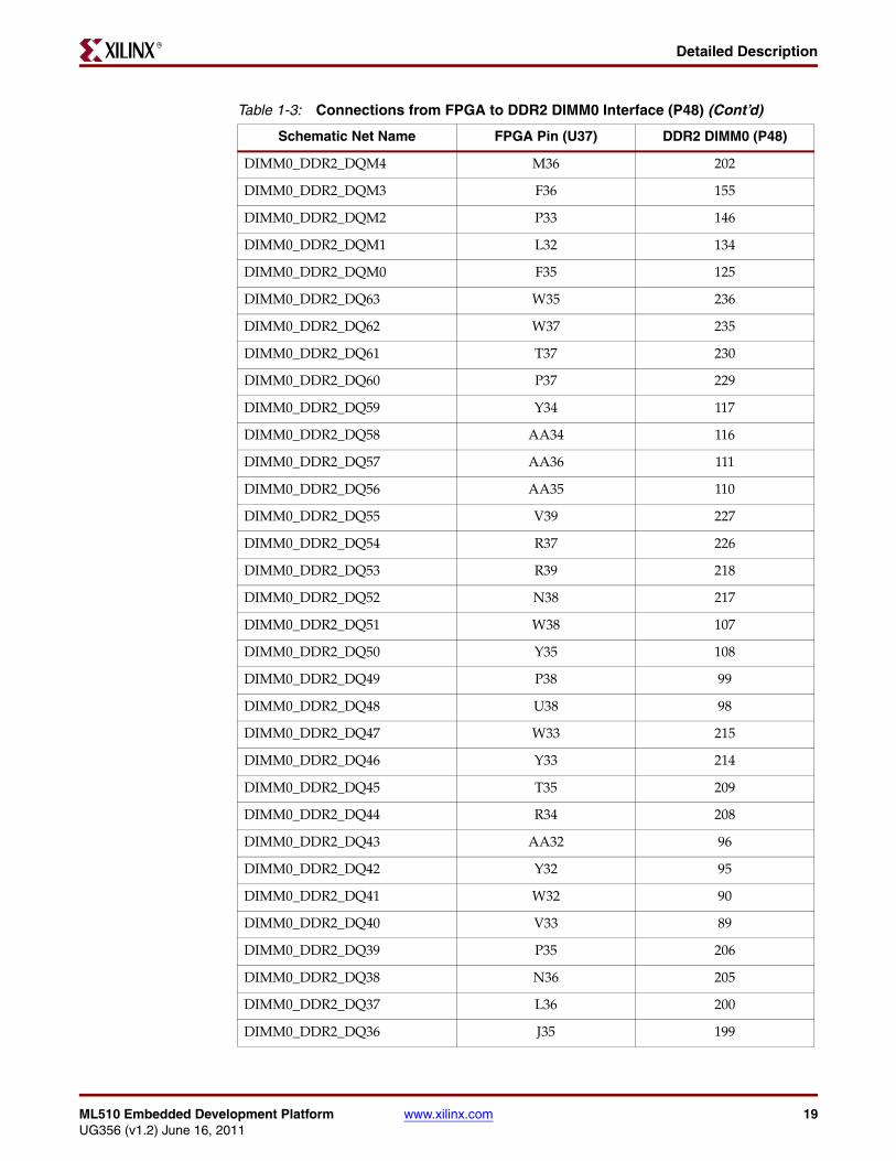
Table 1-3, page 18 describes all the signals associated with DDR2 DIMM component memories. Note that the DDR2_DQ signal names do not correlate because the FPGA uses IBM notation, big endian, while the DDR2 DIMM uses Intel notation, little endian.
Table 1-3: Connections from FPGA to DDR2 DIMM0 Interface (P48)
Schematic Net Name FPGA Pin (U37) DDR2 DIMM0 (P48)
DIMM0_DDR2_WE_B Y40 73
DIMM0_DDR2_S1_B M37 77
DIMM0_DDR2_S0_B U32 193
DIMM0_DDR2_RAS_B W40 192
DIMM0_DDR2_CAS_B AA37 74
DIMM0_DDR2_PLL_CLKIN_P AA40 138
DIMM0_DDR2_PLL_CLKIN_N AA39 137
DIMM0_DDR2_ODT1 K35 76
DIMM0_DDR2_ODT0 U31 195
DIMM0_DDR2_DQS8_P H40 46
DIMM0_DDR2_DQS8_N J40 45
DIMM0_DDR2_DQS7_P K38 114
DIMM0_DDR2_DQS7_N J38 113
DIMM0_DDR2_DQS6_P M38 105
DIMM0_DDR2_DQS6_N L39 104
DIMM0_DDR2_DQS5_P U36 93
DIMM0_DDR2_DQS5_N V36 92
DIMM0_DDR2_DQS4_P R35 84
DIMM0_DDR2_DQS4_N T36 83
DIMM0_DDR2_DQS3_P T34 37
DIMM0_DDR2_DQS3_N U33 36
DIMM0_DDR2_DQS2_P E32 28
DIMM0_DDR2_DQS2_N E33 27
DIMM0_DDR2_DQS1_P F31 16
DIMM0_DDR2_DQS1_N F32 15
DIMM0_DDR2_DQS0_P E34 7
DIMM0_DDR2_DQS0_N F34 6
DIMM0_DDR2_DQM8 G39 164
DIMM0_DDR2_DQM7 W36 232
DIMM0_DDR2_DQM6 T39 223
DIMM0_DDR2_DQM5 V35 211
ML510 Embedded Development Platform www.xilinx.com 19UG356 (v1.2) June 16, 2011
Detailed DescriptionR
DIMM0_DDR2_DQM4 M36 202
DIMM0_DDR2_DQM3 F36 155
DIMM0_DDR2_DQM2 P33 146
DIMM0_DDR2_DQM1 L32 134
DIMM0_DDR2_DQM0 F35 125
DIMM0_DDR2_DQ63 W35 236
DIMM0_DDR2_DQ62 W37 235
DIMM0_DDR2_DQ61 T37 230
DIMM0_DDR2_DQ60 P37 229
DIMM0_DDR2_DQ59 Y34 117
DIMM0_DDR2_DQ58 AA34 116
DIMM0_DDR2_DQ57 AA36 111
DIMM0_DDR2_DQ56 AA35 110
DIMM0_DDR2_DQ55 V39 227
DIMM0_DDR2_DQ54 R37 226
DIMM0_DDR2_DQ53 R39 218
DIMM0_DDR2_DQ52 N38 217
DIMM0_DDR2_DQ51 W38 107
DIMM0_DDR2_DQ50 Y35 108
DIMM0_DDR2_DQ49 P38 99
DIMM0_DDR2_DQ48 U38 98
DIMM0_DDR2_DQ47 W33 215
DIMM0_DDR2_DQ46 Y33 214
DIMM0_DDR2_DQ45 T35 209
DIMM0_DDR2_DQ44 R34 208
DIMM0_DDR2_DQ43 AA32 96
DIMM0_DDR2_DQ42 Y32 95
DIMM0_DDR2_DQ41 W32 90
DIMM0_DDR2_DQ40 V33 89
DIMM0_DDR2_DQ39 P35 206
DIMM0_DDR2_DQ38 N36 205
DIMM0_DDR2_DQ37 L36 200
DIMM0_DDR2_DQ36 J35 199
Table 1-3: Connections from FPGA to DDR2 DIMM0 Interface (P48) (Cont’d)
Schematic Net Name FPGA Pin (U37) DDR2 DIMM0 (P48)

20 www.xilinx.com ML510 Embedded Development PlatformUG356 (v1.2) June 16, 2011
Chapter 1: ML510 Embedded Development PlatformR
DIMM0_DDR2_DQ35 U34 87
DIMM0_DDR2_DQ34 V34 86
DIMM0_DDR2_DQ33 P36 81
DIMM0_DDR2_DQ32 N35 80
DIMM0_DDR2_DQ31 J37 159
DIMM0_DDR2_DQ30 H35 158
DIMM0_DDR2_DQ29 E38 153
DIMM0_DDR2_DQ28 D37 152
DIMM0_DDR2_DQ27 K37 40
DIMM0_DDR2_DQ26 J36 39
DIMM0_DDR2_DQ25 G36 34
DIMM0_DDR2_DQ24 F37 33
DIMM0_DDR2_DQ23 T31 150
DIMM0_DDR2_DQ22 R32 149
DIMM0_DDR2_DQ21 P31 144
DIMM0_DDR2_DQ20 N34 143
DIMM0_DDR2_DQ19 T32 31
DIMM0_DDR2_DQ18 R33 30
DIMM0_DDR2_DQ17 P32 25
DIMM0_DDR2_DQ16 N33 24
DIMM0_DDR2_DQ15 N31 141
DIMM0_DDR2_DQ14 M32 140
DIMM0_DDR2_DQ13 K33 132
DIMM0_DDR2_DQ12 K32 131
DIMM0_DDR2_DQ11 M34 22
DIMM0_DDR2_DQ10 M33 21
DIMM0_DDR2_DQ9 L31 13
DIMM0_DDR2_DQ8 J33 12
DIMM0_DDR2_DQ7 H34 129
DIMM0_DDR2_DQ6 H31 128
DIMM0_DDR2_DQ5 G33 123
DIMM0_DDR2_DQ4 G32 122
DIMM0_DDR2_DQ3 H33 10
Table 1-3: Connections from FPGA to DDR2 DIMM0 Interface (P48) (Cont’d)
Schematic Net Name FPGA Pin (U37) DDR2 DIMM0 (P48)

ML510 Embedded Development Platform www.xilinx.com 21UG356 (v1.2) June 16, 2011
Detailed DescriptionR
DIMM0_DDR2_DQ2 J31 9
DIMM0_DDR2_DQ1 G31 4
DIMM0_DDR2_DQ0 E35 3
DIMM0_DDR2_CKE1 L37 171
DIMM0_DDR2_CKE0 M31 52
DIMM0_DDR2_CB7 H39 168
DIMM0_DDR2_CB6 G38 167
DIMM0_DDR2_CB5 E39 162
DIMM0_DDR2_CB4 E40 161
DIMM0_DDR2_CB3 H38 49
DIMM0_DDR2_CB2 K40 48
DIMM0_DDR2_CB1 F39 43
DIMM0_DDR2_CB0 F40 42
DIMM0_DDR2_CAS_B AA37 74
DIMM0_DDR2_BA2 K39 54
DIMM0_DDR2_BA1 M39 190
DIMM0_DDR2_BA0 N39 71
DIMM0_DDR2_A13 Y37 196
DIMM0_DDR2_A12 N41 176
DIMM0_DDR2_A11 N40 57
DIMM0_DDR2_A10 AA41 70
DIMM0_DDR2_A9 L40 177
DIMM0_DDR2_A8 P42 179
DIMM0_DDR2_A7 R42 58
DIMM0_DDR2_A6 P41 180
DIMM0_DDR2_A5 T40 60
DIMM0_DDR2_A4 U42 61
DIMM0_DDR2_A3 T42 182
DIMM0_DDR2_A2 U41 63
DIMM0_DDR2_A1 P40 183
DIMM0_DDR2_A0 AA42 188
Table 1-3: Connections from FPGA to DDR2 DIMM0 Interface (P48) (Cont’d)
Schematic Net Name FPGA Pin (U37) DDR2 DIMM0 (P48)

22 www.xilinx.com ML510 Embedded Development PlatformUG356 (v1.2) June 16, 2011
Chapter 1: ML510 Embedded Development PlatformR
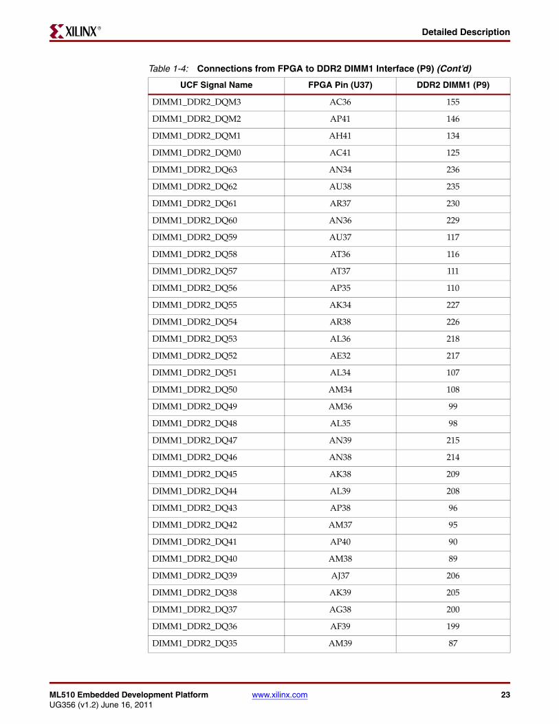
Table 1-4: Connections from FPGA to DDR2 DIMM1 Interface (P9)
UCF Signal Name FPGA Pin (U37) DDR2 DIMM1 (P9)
DIMM1_DDR2_WE_B V40 73
DIMM1_DDR2_S1_B AE37 77
DIMM1_DDR2_S0_B AU42 193
DIMM1_DDR2_RAS_B V41 192
DIMM1_DDR2_CAS_B Y42 74
DIMM1_DDR2_PLL_CLKIN_P Y39 138
DIMM1_DDR2_PLL_CLKIN_N Y38 137
DIMM1_DDR2_ODT1 AF37 76
DIMM1_DDR2_ODT0 AV41 195
DIMM1_DDR2_DQS8_P AH34 46
DIMM1_DDR2_DQS8_N AG34 45
DIMM1_DDR2_DQS7_P AF35 114
DIMM1_DDR2_DQS7_N AF36 113
DIMM1_DDR2_DQS6_P AE35 105
DIMM1_DDR2_DQS6_N AF34 104
DIMM1_DDR2_DQS5_P AT39 93
DIMM1_DDR2_DQS5_N AR39 92
DIMM1_DDR2_DQS4_P AV40 84
DIMM1_DDR2_DQS4_N AU39 83
DIMM1_DDR2_DQS3_P AR40 37
DIMM1_DDR2_DQS3_N AT40 36
DIMM1_DDR2_DQS2_P AC40 28
DIMM1_DDR2_DQS2_N AC39 27
DIMM1_DDR2_DQS1_P AE40 16
DIMM1_DDR2_DQS1_N AD40 15
DIMM1_DDR2_DQS0_P AB39 7
DIMM1_DDR2_DQS0_N AC38 6
DIMM1_DDR2_DQM8 AD33 164
DIMM1_DDR2_DQM7 AV39 232
DIMM1_DDR2_DQM6 AK35 223
DIMM1_DDR2_DQM5 AN40 211
DIMM1_DDR2_DQM4 AG37 202
ML510 Embedded Development Platform www.xilinx.com 23UG356 (v1.2) June 16, 2011
Detailed DescriptionR
DIMM1_DDR2_DQM3 AC36 155
DIMM1_DDR2_DQM2 AP41 146
DIMM1_DDR2_DQM1 AH41 134
DIMM1_DDR2_DQM0 AC41 125
DIMM1_DDR2_DQ63 AN34 236
DIMM1_DDR2_DQ62 AU38 235
DIMM1_DDR2_DQ61 AR37 230
DIMM1_DDR2_DQ60 AN36 229
DIMM1_DDR2_DQ59 AU37 117
DIMM1_DDR2_DQ58 AT36 116
DIMM1_DDR2_DQ57 AT37 111
DIMM1_DDR2_DQ56 AP35 110
DIMM1_DDR2_DQ55 AK34 227
DIMM1_DDR2_DQ54 AR38 226
DIMM1_DDR2_DQ53 AL36 218
DIMM1_DDR2_DQ52 AE32 217
DIMM1_DDR2_DQ51 AL34 107
DIMM1_DDR2_DQ50 AM34 108
DIMM1_DDR2_DQ49 AM36 99
DIMM1_DDR2_DQ48 AL35 98
DIMM1_DDR2_DQ47 AN39 215
DIMM1_DDR2_DQ46 AN38 214
DIMM1_DDR2_DQ45 AK38 209
DIMM1_DDR2_DQ44 AL39 208
DIMM1_DDR2_DQ43 AP38 96
DIMM1_DDR2_DQ42 AM37 95
DIMM1_DDR2_DQ41 AP40 90
DIMM1_DDR2_DQ40 AM38 89
DIMM1_DDR2_DQ39 AJ37 206
DIMM1_DDR2_DQ38 AK39 205
DIMM1_DDR2_DQ37 AG38 200
DIMM1_DDR2_DQ36 AF39 199
DIMM1_DDR2_DQ35 AM39 87
Table 1-4: Connections from FPGA to DDR2 DIMM1 Interface (P9) (Cont’d)
UCF Signal Name FPGA Pin (U37) DDR2 DIMM1 (P9)

24 www.xilinx.com ML510 Embedded Development PlatformUG356 (v1.2) June 16, 2011
Chapter 1: ML510 Embedded Development PlatformR
DIMM1_DDR2_DQ34 AL37 86
DIMM1_DDR2_DQ33 AH38 81
DIMM1_DDR2_DQ32 AJ38 80
DIMM1_DDR2_DQ31 AD37 159
DIMM1_DDR2_DQ30 AD35 158
DIMM1_DDR2_DQ29 AC35 153
DIMM1_DDR2_DQ28 AB34 152
DIMM1_DDR2_DQ27 AE38 40
DIMM1_DDR2_DQ26 AD36 39
DIMM1_DDR2_DQ25 AC34 34
DIMM1_DDR2_DQ24 AB36 33
DIMM1_DDR2_DQ23 AT41 150
DIMM1_DDR2_DQ22 AT42 149
DIMM1_DDR2_DQ21 AM41 144
DIMM1_DDR2_DQ20 AN41 143
DIMM1_DDR2_DQ19 AR42 31
DIMM1_DDR2_DQ18 AP42 30
DIMM1_DDR2_DQ17 AL42 25
DIMM1_DDR2_DQ16 AK42 24
DIMM1_DDR2_DQ15 AL41 141
DIMM1_DDR2_DQ14 AJ42 140
DIMM1_DDR2_DQ13 AH40 132
DIMM1_DDR2_DQ12 AG42 131
DIMM1_DDR2_DQ11 AJ40 22
DIMM1_DDR2_DQ10 AJ41 21
DIMM1_DDR2_DQ9 AF42 13
DIMM1_DDR2_DQ8 AE42 12
DIMM1_DDR2_DQ7 AF41 129
DIMM1_DDR2_DQ6 AF40 128
DIMM1_DDR2_DQ5 AB42 123
DIMM1_DDR2_DQ4 AB41 122
DIMM1_DDR2_DQ3 AD41 10
DIMM1_DDR2_DQ2 AD42 9
Table 1-4: Connections from FPGA to DDR2 DIMM1 Interface (P9) (Cont’d)
UCF Signal Name FPGA Pin (U37) DDR2 DIMM1 (P9)
ML510 Embedded Development Platform www.xilinx.com 25UG356 (v1.2) June 16, 2011
Detailed DescriptionR
DIMM1_DDR2_DQ1 AB37 4
DIMM1_DDR2_DQ0 AB38 3
DIMM1_DDR2_CKE1 AE39 171
DIMM1_DDR2_CKE0 AU41 52
DIMM1_DDR2_CB7 AE33 168
DIMM1_DDR2_CB6 AE34 167
DIMM1_DDR2_CB5 AC33 162
DIMM1_DDR2_CB4 AB32 161
DIMM1_DDR2_CB3 AH36 49
DIMM1_DDR2_CB2 AG36 48
DIMM1_DDR2_CB1 AD32 43
DIMM1_DDR2_CB0 AB33 42
DIMM1_DDR2_CAS_B Y42 74
DIMM1_DDR2_BA2 AH35 54
DIMM1_DDR2_BA1 AJ36 190
DIMM1_DDR2_BA0 AJ35 71
DIMM1_DDR2_A13 W41 196
DIMM1_DDR2_A12 F41 176
DIMM1_DDR2_A11 G41 57
DIMM1_DDR2_A10 W42 70
DIMM1_DDR2_A9 F42 177
DIMM1_DDR2_A8 G42 179
DIMM1_DDR2_A7 J42 58
DIMM1_DDR2_A6 H41 180
DIMM1_DDR2_A5 M42 60
DIMM1_DDR2_A4 L42 61
DIMM1_DDR2_A3 K42 182
DIMM1_DDR2_A2 M41 63
DIMM1_DDR2_A1 J41 183
DIMM1_DDR2_A0 R40 188
Table 1-4: Connections from FPGA to DDR2 DIMM1 Interface (P9) (Cont’d)
UCF Signal Name FPGA Pin (U37) DDR2 DIMM1 (P9)
26 www.xilinx.com ML510 Embedded Development PlatformUG356 (v1.2) June 16, 2011
Chapter 1: ML510 Embedded Development PlatformR
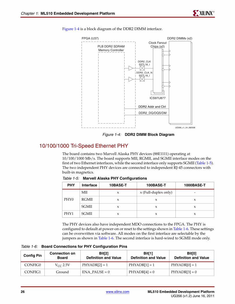
Figure 1-4 is a block diagram of the DDR2 DIMM interface.
10/100/1000 Tri-Speed Ethernet PHYThe board contains two Marvell Alaska PHY devices (88E1111) operating at 10/100/1000 Mb/s. The board supports MII, RGMII, and SGMII interface modes on the first of two Ethernet interfaces, while the second interface only supports SGMII (Table 1-5). The two independent PHY devices are connected to independent RJ-45 connectors with built-in magnetics.
The PHY devices also have independent MDO connections to the FPGA. The PHY is configured to default at power-on or reset to the settings shown in Table 1-6. These settings can be overwritten via software. All modes on the first interface are selectable by the jumpers as shown in Table 1-6. The second interface is hard-wired to SGMII mode only.
X-Ref Target - Figure 1-4
Figure 1-4: DDR2 DIMM Block Diagram
UG356_c1_04_082508
PLB DDR2 SDRAMMemory Controller
FPGA (U37) DDR2 DIMMs (x2)Clock Fanout
Chips (x2)
ICS97U877
DDR2_DQ/DQS/DM
DDR2 Addr and Ctrl
DDR2_CLK_NSSTL18_I
DDR2_CLKSSTL18_I
Table 1-5: Marvell Alaska PHY Configurations
PHY Interface 10BASE-T 100BASE-T 1000BASE-T
PHY0
MII x x (Full-duplex only) -
RGMII x x x
SGMII x x x
PHY1 SGMII x x x
Table 1-6: Board Connections for PHY Configuration Pins
Config PinConnection on
BoardBit[2]
Definition and ValueBit[1]
Definition and ValueBit[0]
Definition and Value
CONFIG0 VCC 2.5V PHYADR[2] = 1 PHYADR[1] = 1 PHYADR[0] = 1
CONFIG1 Ground ENA_PAUSE = 0 PHYADR[4] = 0 PHYADR[3] = 0
ML510 Embedded Development Platform www.xilinx.com 27UG356 (v1.2) June 16, 2011
Detailed DescriptionR
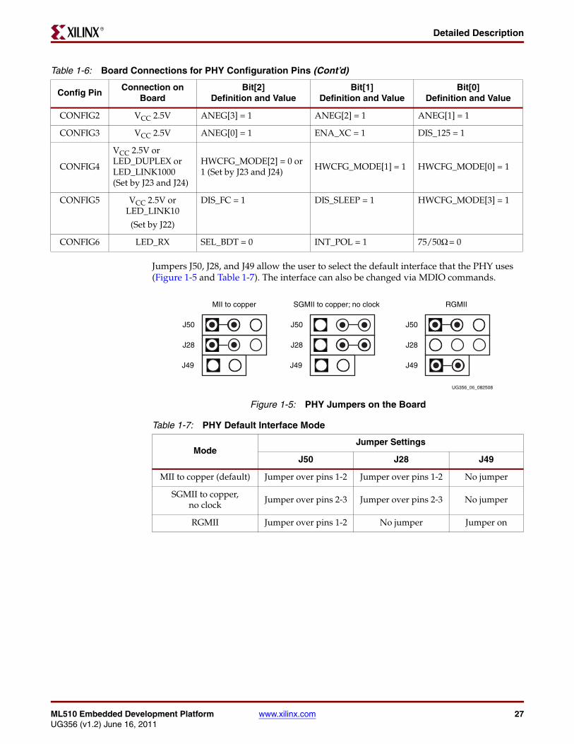
Jumpers J50, J28, and J49 allow the user to select the default interface that the PHY uses (Figure 1-5 and Table 1-7). The interface can also be changed via MDIO commands.
CONFIG2 VCC 2.5V ANEG[3] = 1 ANEG[2] = 1 ANEG[1] = 1
CONFIG3 VCC 2.5V ANEG[0] = 1 ENA_XC = 1 DIS_125 = 1
CONFIG4
VCC 2.5V or LED_DUPLEX or LED_LINK1000 (Set by J23 and J24)
HWCFG_MODE[2] = 0 or 1 (Set by J23 and J24) HWCFG_MODE[1] = 1 HWCFG_MODE[0] = 1
CONFIG5 VCC 2.5V or LED_LINK10
(Set by J22)
DIS_FC = 1 DIS_SLEEP = 1 HWCFG_MODE[3] = 1
CONFIG6 LED_RX SEL_BDT = 0 INT_POL = 1 75/50Ω = 0
Table 1-6: Board Connections for PHY Configuration Pins (Cont’d)
Config PinConnection on
BoardBit[2]
Definition and ValueBit[1]
Definition and ValueBit[0]
Definition and Value
X-Ref Target - Figure 1-5
Figure 1-5: PHY Jumpers on the Board
Table 1-7: PHY Default Interface Mode
ModeJumper Settings
J50 J28 J49
MII to copper (default) Jumper over pins 1-2 Jumper over pins 1-2 No jumper
SGMII to copper, no clock
Jumper over pins 2-3 Jumper over pins 2-3 No jumper
RGMII Jumper over pins 1-2 No jumper Jumper on
UG356_06_082508
J50
J28
MII to copper
J50
J28
SGMII to copper; no clock
J50
J28
RGMII
J49J49J49

28 www.xilinx.com ML510 Embedded Development PlatformUG356 (v1.2) June 16, 2011
Chapter 1: ML510 Embedded Development PlatformR
Figure 1-6 shows the PHY0 MII interface.
Figure 1-7 shows the PHY0 RGMII interface.
X-Ref Target - Figure 1-6
Figure 1-6: MII Interface
X-Ref Target - Figure 1-7
Figure 1-7: RGMII Interface
PHY0_TXER
PHY0_TXCLK
UG356_c1_6_082508
PHY0_TXCTL_TXEN
PHY0_TXD[3:0]
PHY0_RXER
PHY0_RXCLK
PHY0_RXCTL_RXDV
PHY0_RXD[3:0]
PHY0_RESET
PHY0_INT
PHY0_MDC
PHY0_MDIO
FPGA PHY0 (U47)
PHY0_GTXCLK
UG356_c1_07_082508
PHY0_TXCTL_TXEN
PHY0_TXD[3:0]
PHY0_RXCLK
PHY0_RXCTL_RXDV
PHY0_RXD[3:0]
PHY0_RESET
PHY0_INT
PHY0_MDC
PHY0_MDIO
FPGA PHY0 (U47)

ML510 Embedded Development Platform www.xilinx.com 29UG356 (v1.2) June 16, 2011
Detailed DescriptionR
Figure 1-8 shows the PHY0 and PHY1 SGMII interface. X-Ref Target - Figure 1-8
Figure 1-8: SGMII Interface
Table 1-8: PHY0 MII/RGMII/SGMII Interfaces
Signal Name FPGA Pin MII RGMII SGMII Description
PHY0_TX_CLK M26 x MII transmit clock
PHY0_RXC_CLK J17 x x MII/RGMII receive clock
PHY0_GTX_CLK AM31 x RGMII transmit clock
PHY0_TXD3 AN31 x x
Transmit data bitsPHY0_TXD2 AR32 x x
PHY0_TXD1 AP32 x x
PHY0_TXD0 AR33 x x
PHY0_TXER AT31 xTransmit controls
PHY0_TXCTL_TXEN AP31 x x
PHY0_RX_D3 AM33 x x
Receive data bitsPHY0_RX_D2 AK33 x x
PHY0_RX_D1 AJ33 x x
PHY0_RX_D0 AJ32 x x
PHY0_TXD_P
UG356_c1_08_082508
PHY0_TXD_N
PHY0_RXD_P
PHY0_RXD_N
PHY0_MDC
PHY0_MDIO
PHY0_RESET
PHY0_INT
PHY1_TXD_P
PHY1_TXD_N
PHY1_RXD_P
PHY1_RXD_N
SGMIICLK_P
SGMIICLK_N
PHY1_MDC
PHY1_MDIO
PHY1_RESET
PHY1_INT
FPGA PHY0 (U47)
PHY1 (U53)

30 www.xilinx.com ML510 Embedded Development PlatformUG356 (v1.2) June 16, 2011
Chapter 1: ML510 Embedded Development PlatformR
PHY0_RXER AP33 xReceive controls
PHY0_RXCTL_RXDV AN33 x x
PHY0_SGMII_TX_P B6 xSGMII transmit pair (GTX)
PHY0_SGMII_TX_N B5 x
PHY0_SGMII_RX_P A5 xSGMII receive pair (GTX)
PHY0_SGMII_RX_N A4 x
PHY0_INT AL32 x x x PHY interrupt
PHY0_RESET AK32 x x x PHY reset
PHY0_MDIO AL31 x x xPHY management data input/output
PHY0_MDC AM32 x x xPHY management data clock
Table 1-9: PHY1 SGMII Interface
Signal Name FPGA Pin MII RGMII SGMII Description
PHY1_SGMII_TX_P B1 xSGMII transmit pair (GTX)
PHY1_SGMII_TX_N B2 x
PHY1_SGMII_RX_P A2 xSGMII receive pair (GTX)
PHY1_SGMII_RX_N A3 x
PHY1_INT AV31 x x x PHY interrupt
PHY1_RESET AL25 x x x PHY reset
PHY1_MDIO AT32 x x x PHY management data input/output
PHY1_MDC AU31 x x x PHY management data clock
SGMIICLK_P C4 x SGMII REFCLK 125 MHz (GTX)SGMIICLK_N C3 x
Table 1-8: PHY0 MII/RGMII/SGMII Interfaces (Cont’d)
Signal Name FPGA Pin MII RGMII SGMII Description

ML510 Embedded Development Platform www.xilinx.com 31UG356 (v1.2) June 16, 2011
Detailed DescriptionR
System ACE and CompactFlash ConnectorThe Xilinx System ACE CompactFlash (CF) configuration controller allows a Type I CompactFlash card to program the FPGA through the JTAG port. Both hardware and software data can be downloaded through the JTAG port. The System ACE controller supports up to eight configuration images on a single CompactFlash card. The configuration address switches allow the user to choose which of the eight configuration images to use.
System ACE error and status LEDs indicate the operational state of the System ACE controller:
• A blinking red error LED indicates that no CompactFlash card is present
• A solid red error LED indicates an error condition during configuration
• A blinking green status LED indicates a configuration operation is ongoing
• A solid green status LED indicates a successful download
Every time a CompactFlash card is inserted into the System ACE socket, a configuration operation is initiated. Pressing the System ACE reset button re-programs the FPGA.
The board also features a System ACE failsafe mode. In this mode, if the System ACE controller detects a failed configuration attempt, it automatically reboots back to a predefined configuration image. The failsafe mode is enabled by inserting two jumpers across J18 and J19 (in horizontal or vertical orientation).
Caution! Use caution when inserting a CompactFlash card with exposed metallic surfaces. Improper insertion can cause a short with the traces or components on the board.
Note: The System ACE configuration address pins are shared with the BPI flash RS[1:0] pins on the FPGA. When manually selecting a different System ACE configuration with dual-inline package (DIP) switch SW3, users must press the PROGRAM pushbutton first and then press the SysAce Reset pushbutton. This is required only if there is a Flash interface such as the EDK XPS_EMC pcore driving the RS[1:0] pins as address lines. Configuration selections made via the MPU interface are not affected by the Flash interface already loaded in the the FPGA design.
The System ACE MPU port is connected to the FPGA. This connection allows the FPGA to use the System ACE controller to reconfigure the system or access the CompactFlash card as a generic FAT file system. The data bus for the System ACE MPU port is shared with the USB controller. See “Non-Volatile Storage through the MPU Interface,” page 33.
32 www.xilinx.com ML510 Embedded Development PlatformUG356 (v1.2) June 16, 2011
Chapter 1: ML510 Embedded Development PlatformR
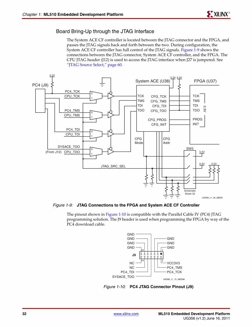
Board Bring-Up through the JTAG Interface
The System ACE CF controller is located between the JTAG connector and the FPGA, and passes the JTAG signals back and forth between the two. During configuration, the System ACE CF controller has full control of the JTAG signals. Figure 1-9 shows the connections between the JTAG connector, System ACE CF controller, and the FPGA. The CPU JTAG header (J12) is used to access the JTAG interface when J27 is jumpered. See “JTAG Source Select,” page 60.
The pinout shown in Figure 1-10 is compatible with the Parallel Cable IV (PC4) JTAG programming solution. The J9 header is used when programming the FPGA by way of the PC4 download cable.
X-Ref Target - Figure 1-9
Figure 1-9: JTAG Connections to the FPGA and System ACE CF Controller
PC4 (J9)System ACE (U38) FPGA (U37)
CPU_TCK
CPU_TMS
CPU_TDI
CPU_TDO(From J12)
PC4_TCK
JTAG_SRC_SEL
TCKTMSTDITDO
TCKTMSTDITDO
PROG
3.3V
INIT
CFG_TCKCFG_TMSCFG_TDI
CFG_TDO
CFG_PROGCFG_INIT
PC4_TMS
PC4_TDI
SYSACE_TDO
0
1
3.3V3.3V
0
1
0
1
0
1
SW3
SchematicSheet 33
CFGMode
CFGAddr
3.3V
3.3V
UG356_c1_09_082508
3.3V
3.3V
X-Ref Target - Figure 1-10
Figure 1-10: PC4 JTAG Connector Pinout (J9)
1
214
13
GNDGND
GND
PC4_TMSPC4_TCK
VCC3V3
SYSACE_TDOPC4_TDI
NCNC
GNDGNDGNDGND
UG356_c1_10_082508
J9
ML510 Embedded Development Platform www.xilinx.com 33UG356 (v1.2) June 16, 2011
Detailed DescriptionR
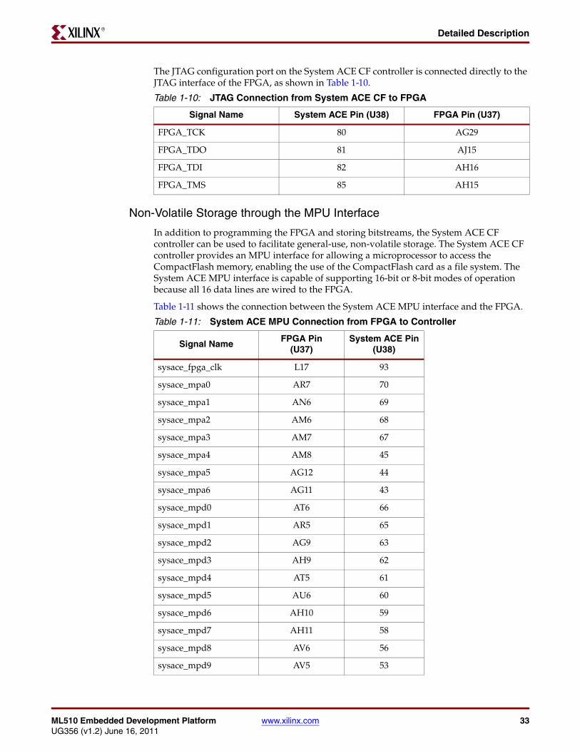
The JTAG configuration port on the System ACE CF controller is connected directly to the JTAG interface of the FPGA, as shown in Table 1-10.
Non-Volatile Storage through the MPU Interface
In addition to programming the FPGA and storing bitstreams, the System ACE CF controller can be used to facilitate general-use, non-volatile storage. The System ACE CF controller provides an MPU interface for allowing a microprocessor to access the CompactFlash memory, enabling the use of the CompactFlash card as a file system. The System ACE MPU interface is capable of supporting 16-bit or 8-bit modes of operation because all 16 data lines are wired to the FPGA.
Table 1-11 shows the connection between the System ACE MPU interface and the FPGA.
Table 1-10: JTAG Connection from System ACE CF to FPGA
Signal Name System ACE Pin (U38) FPGA Pin (U37)
FPGA_TCK 80 AG29
FPGA_TDO 81 AJ15
FPGA_TDI 82 AH16
FPGA_TMS 85 AH15
Table 1-11: System ACE MPU Connection from FPGA to Controller
Signal NameFPGA Pin
(U37)System ACE Pin
(U38)
sysace_fpga_clk L17 93
sysace_mpa0 AR7 70
sysace_mpa1 AN6 69
sysace_mpa2 AM6 68
sysace_mpa3 AM7 67
sysace_mpa4 AM8 45
sysace_mpa5 AG12 44
sysace_mpa6 AG11 43
sysace_mpd0 AT6 66
sysace_mpd1 AR5 65
sysace_mpd2 AG9 63
sysace_mpd3 AH9 62
sysace_mpd4 AT5 61
sysace_mpd5 AU6 60
sysace_mpd6 AH10 59
sysace_mpd7 AH11 58
sysace_mpd8 AV6 56
sysace_mpd9 AV5 53

34 www.xilinx.com ML510 Embedded Development PlatformUG356 (v1.2) June 16, 2011
Chapter 1: ML510 Embedded Development PlatformR
Linear Flash MemoryA 16-bit wide NOR linear flash device (Intel JS28F256P30T95) is installed on the board to provide 256 Mb of flash memory (Figure 1-11). This memory provides non-volatile storage of data, software, or bitstreams. The flash memory can also be used to program the FPGA.
Note: The System ACE configuration address lines, CFG[0:1], are shared with the upper address lines of the BPI flash device. Because these connections are shared, before manually moving to a different System ACE configuration file the user must first pulse the PROG pushbutton before pulsing the System ACE Reset pushbutton. This is required only when the user has implemented a design that drives the flash address lines, such as the EDK EMC controller.
SYSACE_MPD10 AJ11 52
sysace_mpd11 AJ10 51
sysace_mpd12 AJ8 50
sysace_mpd13 AT7 49
sysace_mpd14 AP8 48
sysace_mpd15 AK8 47
sysace_mpoe AK10 77
sysace_mpce AN18 42
sysace_mpwe AR8 76
sysace_mpirq AK9 41
Table 1-11: System ACE MPU Connection from FPGA to Controller (Cont’d)
Signal NameFPGA Pin
(U37)System ACE Pin
(U38)

ML510 Embedded Development Platform www.xilinx.com 35UG356 (v1.2) June 16, 2011
Detailed DescriptionR
X-Ref Target - Figure 1-11
Figure 1-11: BPI Linear Flash Connectivity
A0
A1
A2
A20
A21
A22
RS0
RS1
A1
A2
A3
A21
A22
A23
A24
R496
R495
CF
G1
CF
G0
CF
G2
R479
R493
3.3V
SW3
AK14
AK13
AK12
FPGA FLASH
SYSTEM ACE
CFG2CFG1CFG0
32 MB BPI FlashUse RS[0:1] to select 4 x 8 MB bit files
This configuration allows for SW3 to preset the RS0 and RS1 pin on the FPGA to select any ofthe 4 bitstreams stored at each 1/4 location inthe BPI flash.
BPI-Up BPI-Down0x0000 0000 0x0200 00000x0080 0000 0x0180 00000x0100 0000 0x0100 00000x0180 0000 0x0080 0000
FLASH_A0FLASH_A1FLASH_A2
FLASH_A20FLASH_A21
UG356_c1_11_082508
Table 1-12: Linear Flash Connection from FPGA to Strata Flash (U43)
Signal Name FPGA Pin (U37) Strata Flash (U43)
FLASH_WE_B AM28 14
FLASH_WAIT W11 56
FLASH_RESET_B K7 44
FLASH_OE_B AM13 32
FLASH_D15 AN30 54
FLASH_D14 AP30 52
FLASH_D13 AK17 50
FLASH_D12 AL17 48
FLASH_D11 AN29 42
FLASH_D10 AP28 40
FLASH_D9 AL15 37
36 www.xilinx.com ML510 Embedded Development PlatformUG356 (v1.2) June 16, 2011
Chapter 1: ML510 Embedded Development PlatformR
FLASH_D8 AL16 35
FLASH_D7 AN13 53
FLASH_D6 AP13 51
FLASH_D5 AK28 49
FLASH_D4 AK29 47
FLASH_D3 AN14 41
FLASH_D2 AM14 39
FLASH_D1 AK27 36
FLASH_D0 AJ26 34
FLASH_CLK AN28 45
FLASH_CE_B AL14 30
FLASH_ADV_B AL29 46
FLASH_A21 AL30 10
FLASH_A20 AM29 11
FLASH_A19 N25 16
FLASH_A18 P25 17
FLASH_A17 P18 18
FLASH_A16 P17 55
FLASH_A15 P26 1
FLASH_A14 N26 2
FLASH_A13 M16 3
FLASH_A12 N16 4
FLASH_A11 P27 5
FLASH_A10 P28 6
FLASH_A9 N15 7
FLASH_A8 N14 8
FLASH_A7 N28 19
FLASH_A6 N29 20
FLASH_A5 M14 21
FLASH_A4 M13 22
FLASH_A3 N30 23
FLASH_A2 M29 24
FLASH_A1 N13 25
FLASH_A0 P13 29
Table 1-12: Linear Flash Connection from FPGA to Strata Flash (U43) (Cont’d)
Signal Name FPGA Pin (U37) Strata Flash (U43)
ML510 Embedded Development Platform www.xilinx.com 37UG356 (v1.2) June 16, 2011
Detailed DescriptionR
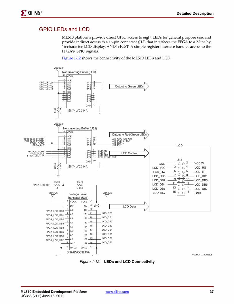
GPIO LEDs and LCDML510 platforms provide direct GPIO access to eight LEDs for general purpose use, and provide indirect access to a 16-pin connector (J13) that interfaces the FPGA to a 2-line by 16-character LCD display, AND491GST. A simple register interface handles access to the FPGA’s GPIO signals.
Figure 1-12 shows the connectivity of the ML510 LEDs and LCD. X-Ref Target - Figure 1-12
Figure 1-12: LEDs and LCD Connectivity
UG356_c1_12_082508
VCC3V3
LCD_RSLCD_ELCD_RWLED_DONE_BUF
919
131517 3
57
11
18
20
1
468
10
121416
2
LED_DONELED_PLB_ERRORLED_OPB_ERROR
FPGA_LCD_RS
FPGA_DONE
OPB_BUS_ERRORPLB_BUS_ERROR
4.75
K
R35
8
FPGA_INIT
FPGA_LCD_RWFPGA_LCD_E
LED_INIT
VCC2V5 VCC3V3
SN74LVCC3245A
GND3GND2
GND1
A8
A7
A6
A5
A4
A3
A2
A1
DIR
VCCA
B8
B7
B6
B5
B4
B3
B2
B1
OE
NC
VCCB
FPGA_LCD_DIR
NC
R373
4.75K
R388
0
1312
11
10
9
8
7
6
5
4
3
2
1
14
15
16
17
18
19
20
21
22
23
24
Voltage LevelTranslator (U35)
LCD_DB7
LCD_DB6
LCD_DB5
LCD_DB4
LCD_DB3
LCD_DB2
LCD_DB1
LCD_DB0FPGA_LCD_DB0
FPGA_LCD_DB4
FPGA_LCD_DB5
FPGA_LCD_DB6
FPGA_LCD_DB3
FPGA_LCD_DB2
FPGA_LCD_DB1
FPGA_LCD_DB7
VCC5V
1513
121197
1 235 6
4
810
1416
J13
LCD_BLV
LCD_VLC
LCD_DB3
LCD_DB1
LCD_DB2LCD_DB0LCD_RW
GND
LCD_DB5LCD_DB6
LCD_RS
LCD_DB7
LCD_E
LCD_DB4
GND
VCC3V3
SN74LVC244A
2Y12OE
2A22A32A4 2Y4
2Y32Y2
2A1
1Y1
VCCA
1OE
1A21A31A4
GND
1Y41Y31Y2
1A1
919
131517 3
57
11
18
20
1
468
10
121416
2DBG_LED_0
DBG_LED_3DBG_LED_2DBG_LED_1
4.75
K
R39
9
LCD Control
Output to Red/Green LEDs
Output to Green LEDs
LCD Data
LCD
Non-Inverting Buffer (U36)
Non-Inverting Buffer (U33)
SN74LVC244A
2Y12OE
2A22A32A4 2Y4
2Y32Y2
2A1
1Y1
VCCA
1OE
1A21A31A4
GND
1Y41Y31Y2
1A1
38 www.xilinx.com ML510 Embedded Development PlatformUG356 (v1.2) June 16, 2011
Chapter 1: ML510 Embedded Development PlatformR
GPIO LED Interface
All LEDs connected to the GPIO lines illuminate green when driven with a logic 0 and extinguish with a logic 1. Table 1-13 shows the connections for the GPIO LEDs from the FPGA to the non-inverting buffer (U36). The FPGA GPIO lines are also wired to a DIP switch (SW5). The combinations of LEDs in parallel with a DIP switch allow users to set LEDs when the FPGA is actively driving the GPIOs as outputs. The DIP switch values are available when the GPIOs are used as inputs. Pull-up and pull-down resistors are in place to protect the FPGA pins from any contention condition.
GPIO LCD Interface
The GPIO LCD interface has eight input/output signals used as data and three output-only signals used as control. The data signals are controlled by the logic level of the FPGA_LCD_DIR signal. A logic 1 on FPGA_LCD_DIR configures the LVCC3245 to drive the J13 header, while a logic 0 on FPGA_LCD_DIR configures the LVCC3245 to drive the FPGA.
Table 1-14 shows the data bus signals on the GPIO LCD interface from the FPGA to U35.
Table 1-13: GPIO LED Connection from FPGA to U36
Signal Name FPGA Pin (U37)LVC244
Buffer (U36)LED
DBG_LED_0 AL7 2 DS20
DBG_LED_1 AP6 4 DS19
DBG_LED_2 AN5 6 DS18
DBG_LED_3 AL6 8 DS17
Table 1-14: GPIO LCD Data Signals from FPGA to U35
Signal Name FPGA Pin (U37)LVCC3245 Translator
(U61)
LCD I/F(J13)
FPGA_LCD_DB0 R4 3 7
FPGA_LCD_DB1 R5 4 8
FPGA_LCD_DB2 T5 5 9
FPGA_LCD_DB3 T4 6 10
FPGA_LCD_DB4 AA11 7 11
FPGA_LCD_DB5 AA10 8 12
FPGA_LCD_DB6 AA9 9 13
FPGA_LCD_DB7 Y10 10 14
FPGA_LCD_E W10 2(1) 6
FPGA_LCD_RW Y9 2(1) 5
Notes: 1. FPGA_LCD_E and FPGA_LCD_RW are logically NANDed and the output
connects to U61 pin 2 (Direction control pin of U61).

ML510 Embedded Development Platform www.xilinx.com 39UG356 (v1.2) June 16, 2011
Detailed DescriptionR
The control signals allow the user to read/write the LCD character display in conjunction with the eight LCD data signals defined in Table 1-14. See the AND491GST LCD display data sheet located on the ML510 documentation CD for more information.
Table 1-15 shows the control signal connections for the GPIO LCD from the FPGA to U33.
JTAG Trace/Debug
CPU Debug Description
External-debug mode can be used to alter normal program execution. It provides the ability to debug both system hardware and software. External-debug mode supports setting of multiple breakpoints, as well as monitoring processor status. Access to processor debugging resources is available through the CPU JTAG port (J12) and the Mictor connector (P8), providing the appropriate connections to the FPGA fabric are in place.
The JTAG debug port supports the four required JTAG signals: TCK, TMS, TDI, and TDO. It also implements the optional TRST signal. The frequency of the JTAG clock signal can range from 0 MHz (DC) to one-half of the processor clock frequency. The JTAG debug port logic is reset at the same time the system is reset, using TRST. When TRST is asserted, the JTAG TAP controller returns to the test-logic reset state.
Figure 1-13 shows a 38-pin Mictor connector that combines the CPU Trace and the CPU Debug interfaces for high-speed, controlled-impedance signaling.
Table 1-15: GPIO LCD Control Signals from FPGA to U33
Signal Name FPGA Pin (U37)LVC244 Buffer
(U33)LCD I/F
(J13)
FPGA_LCD_E W10 13 6
FPGA_LCD_RS Y8 11 4
FPGA_LCD_RW Y9 15 5

40 www.xilinx.com ML510 Embedded Development PlatformUG356 (v1.2) June 16, 2011
Chapter 1: ML510 Embedded Development PlatformR
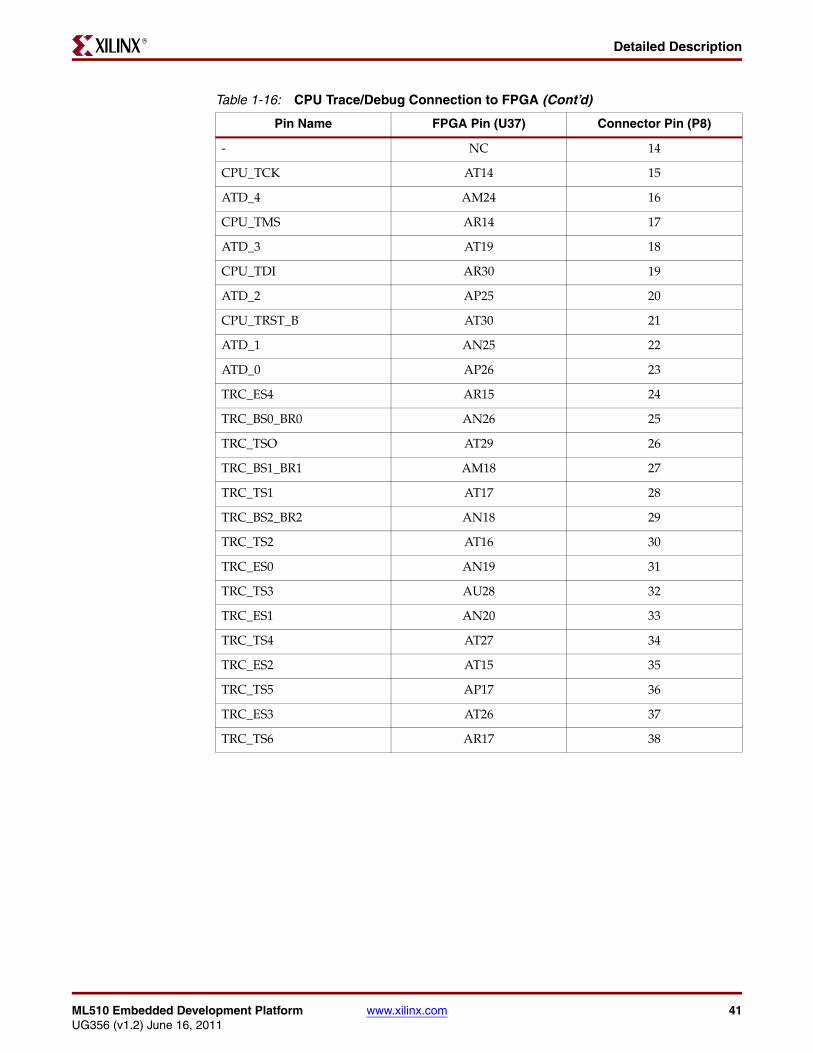
Table 1-16 shows the CPU trace/debug connections from P8 to the FPGA.
X-Ref Target - Figure 1-13
Figure 1-13: Combined Trace/Debug Connector Pinout
Table 1-16: CPU Trace/Debug Connection to FPGA
Pin Name FPGA Pin (U37) Connector Pin (P8)
- NC 1
- NC 2
- NC 3
- NC 4
ATCB_CLK J16 5
TRC_CLK AR27 6
CPU_HALT_B AR29 7
- - 8
- - 9
- - 10
CPU_TDO AR28 11
TRC_VSENSE - 12
- NC 13
373533312927252321191715131197531
CPU_TRST_NCPU_TDICPU_TMSCPU_TCK
NC
NC
NCNCNC
NC
NCNC
NCNC
ATD_12ATD_13ATD_14ATD_15
ATD_8ATD_9ATD_10ATD_11
CPU_TDO
CPU_HALT_NATCB_CLK
TRC_TS6TRC_TS5TRC_TS4TRC_TS3
TRC_TS1ETRC_TS2E
TRC_TS2OTRC_TS1O
ATD_17ATD_16
ATD_18
TRC_CLK
TRC_VSENSE
383634323028262422201816141210
8642
Mictor 38 (P8)
2.5V
UG356_c1_13_082508GND, G1, G2, G3, G4, G5
ML510 Embedded Development Platform www.xilinx.com 41UG356 (v1.2) June 16, 2011
Detailed DescriptionR
- NC 14
CPU_TCK AT14 15
ATD_4 AM24 16
CPU_TMS AR14 17
ATD_3 AT19 18
CPU_TDI AR30 19
ATD_2 AP25 20
CPU_TRST_B AT30 21
ATD_1 AN25 22
ATD_0 AP26 23
TRC_ES4 AR15 24
TRC_BS0_BR0 AN26 25
TRC_TSO AT29 26
TRC_BS1_BR1 AM18 27
TRC_TS1 AT17 28
TRC_BS2_BR2 AN18 29
TRC_TS2 AT16 30
TRC_ES0 AN19 31
TRC_TS3 AU28 32
TRC_ES1 AN20 33
TRC_TS4 AT27 34
TRC_ES2 AT15 35
TRC_TS5 AP17 36
TRC_ES3 AT26 37
TRC_TS6 AR17 38
Table 1-16: CPU Trace/Debug Connection to FPGA (Cont’d)
Pin Name FPGA Pin (U37) Connector Pin (P8)

42 www.xilinx.com ML510 Embedded Development PlatformUG356 (v1.2) June 16, 2011
Chapter 1: ML510 Embedded Development PlatformR
CPU JTAG Header Pinout
Figure 1-14 shows J12, the 16-pin header that can be used to debug the software operating in the CPU with debug tools such as Parallel Cable IV or third party tools.
CPU JTAG Connection to FPGA
The connections between the CPU JTAG header (J12) and the FPGA are shown in Table 1-17. These are attached to the PPC440 JTAG debug resources using normal FPGA routing resources. The JTAG debug resources are not hard-wired to particular pins and are available for attachment in the FPGA fabric, making it possible to route these signals to the preferred FPGA pins.
DVI OutputA DVI connector (P10) is present on the board to support an external video monitor. The DVI circuitry utilizes a Chrontel CH7301C capable of 1600 X 1200 resolution with 24-bit color. The video interface chip drives both the digital and analog signals to the DVI connector. A DVI monitor can be connected to the board directly. A VGA monitor can also be connected to the board using a DVI-to-VGA adaptor. The Chrontel CH7301C is controlled by way of the video IIC bus.
X-Ref Target - Figure 1-14
Figure 1-14: CPU JTAG Header (J12)
1
216
15
UG356_c1_14_08250
GND
CPU_VSENSECPU_TRST_B
CPU_HALT_BCPU_TMS
CPU_TDOJ12
CPU_TDI
CPU_TCK
Table 1-17: CPU JTAG Connection to FPGA
Pin Name FPGA Pin (U37) Connector Pin (J12)
CPU_TDO AR28 1
CPU_TDI AR30 3
CPU_TRST_B AT30 4
CPU_TCK AT14 7
CPU_TMS AR14 9
CPU_HALT_B AR29 11

ML510 Embedded Development Platform www.xilinx.com 43UG356 (v1.2) June 16, 2011
Detailed DescriptionR
The DVI connector (Table 1-18) supports the IIC protocol to allow the board to read the monitor’s configuration parameters. These parameters can be read by the FPGA using the VGA IIC bus.
PCI Express InterfaceML510 platforms that are equipped with PCI Express host connectors (P53 and P54) are capable of supporting PCI Express cores. Power distribution is handled by a MIC2959B dual-slot PCI Express hot-plug controller (Figure 1-15) that also provides comprehensive system protection and fault isolation. The MIC2959B controls the power delivered through MOSFETs to the Slot A (P53) and Slot B (P54) PCI Express connectors. The MIC2592B also incorporates an SMBus interface that provides control for and status of each PCI Express slot.
Although two 16x PCI Express connectors are mounted on ML510 platforms, not all 16 lanes are wired for use.
The PCI Express interface supports GTPs operating at 2.5 Gb/s. Power is activated to the PCI Express slots only when the proper MIC2959B IIC commands are delivered to the MIC2959B at address 0x8E over the IIC interface. For more on IIC, see “IIC/SMBus Interface,” page 53. For details on the power controller, see the MIC2959B data sheet at www.micrel.com. For more on clocking, see “Clock Generation,” page 14.
Table 1-18: DVI Controller Connections
Net Name FPGA Pin
DVI_D0 AP15
DVI_D1 AP16
DVI_D2 AL26
DVI_D3 AL27
DVI_D4 AN16
DVI_D5 AN15
DVI_D6 AM26
DVI_D7 AM27
DVI_D8 AM16
DVI_D9 AK15
DVI_D10 AJ30
DVI_D11 AK30
DVI_XCLK_P AG8
DVI_XCLK_N AH8
DVI_HSYNC AP27
DVI_VSYNC AM17
DVI_DE M8
DVI_RESET_B AM9

44 www.xilinx.com ML510 Embedded Development PlatformUG356 (v1.2) June 16, 2011
Chapter 1: ML510 Embedded Development PlatformR
Table 1-19 and Table 1-20, page 45 detail the connections between the FPGA and the PCI Express connectors.
X-Ref Target - Figure 1-15
Figure 1-15: PCI Express Power Management and Clocking
Table 1-19: Connections from FPGA to PCI Express Slot A
Net Name FPGA Pin (U37) Description
GTP122_PCIE_SLOTA_CLK_P AT4 PCIe SlotA RefCLK 122
GTP122_PCIE_SLOTA_CLK_N AT3 PCIe SlotA RefCLK 122
GTP126_PCIE_SLOTA_CLK_P AW4 PCIe SlotA RefCLK 126
GTP126_PCIE_SLOTA_CLK_N AY4 PCIe SlotA RefCLK 126
PCIE_SLOTA_WAKE_B_R K17 PCIe SlotA WAKE#
PCIE_SLOTA_PRSNT2_B_R M28 PCIe SlotA PRSNT2#
PCIE_SLOTA_PERST_B L27 PCIe SlotA PERST#
GTP_122_TX0_P_C AP2 Lane 1 TX
GTP_122_TX0_N_C AR2 Lane 1 TX
GTP_122_RX0_P AR1 Lane 1 RX
GTP_122_RX0_N AT1 Lane 1 RX
GTP_122_TX1_P_C AW2 Lane 2 TX
GTP_122_TX1_N_C AV2 Lane 2 TX
UG356_c1_15_082508
PCIE Slot A
PCIE Slot B
U14/U16
U51/U52
MOSFETs
MIC2592B
PCI ExpressPower Management
U55ADDR: 0x8E
+3.3
IIC_SCL
IIC_SDA
+12V
+3.3V @ 3A
+12V @ 2.1A
25 MHz
100 MHz(LVPECL)
ICS843011
ICS85104
100 MHz
PCIE_SLOTA_CLK
PCIE_SLOTA_NCLK
PCIE_SLOTB_CLK
PCIE_SLOTB_NCLK
FPGA (U37)
XC5VFX130T
P53
P54
GTP
GTP
GTP
GTP
GTP
GTP
GTP
GTP

ML510 Embedded Development Platform www.xilinx.com 45UG356 (v1.2) June 16, 2011
Detailed DescriptionR
GTP_122_RX1_P AV1 Lane 2 RX
GTP_122_RX1_N AU1 Lane 2 RX
GTP_126_TX0_P_C BA1 Lane 3 TX
GTP_126_TX0_N_C BA2 Lane 3 TX
GTP_126_RX0_P BB2 Lane 3 RX
GTP_126_RX0_N BB3 Lane 3 RX
GTP_126_TX1_P_C BA6 Lane 4 TX
GTP_126_TX1_N_C BA5 Lane 4 TX
GTP_126_RX1_P BB5 Lane 4 RX
GTP_126_RX1_N BB4 Lane 4 RX
GTP_130_TX0_P_C BA7 Lane 5 TX
GTP_130_TX0_N_C BA8 Lane 5 TX
GTP_130_RX0_P BB8 Lane 5 RX
GTP_130_RX0_N BB9 Lane 5 RX
GTP_130_TX1_P_C BA12 Lane 6 TX
GTP_130_TX1_N_C BA11 Lane 6 TX
GTP_130_RX1_P BB11 Lane 6 RX
GTP_130_RX1_N BB10 Lane 6 RX
Table 1-20: Connections from FPGA to PCI Express Slot B
Net Name FPGA Pin (U37) Description
GTP128_PCIE_SLOTB_CLK_P D10 PCIe SlotB RefCLK 128
GTP128_PCIE_SLOTB_CLK_N C10 PCIe SlotB RefCLK 128
GTP132_PCIE_SLOTB_CLK_P D16 PCIe SlotB RefCLK 132
GTP132_PCIE_SLOTB_CLK_N C16 PCIe SlotB RefCLK 132
PCIE_SLOTB_WAKE_B_R J30 PCIe SlotB WAKE#
PCIE_SLOTB_PRSNT2_B_R K15 PCIe SlotB PRSNT2#
PCIE_SLOTB_PERST_B L15 PCIe SlotB PERST#
GTP_128_TX0_P_C B12 Lane 1 TX
GTP_128_TX0_N_C B11 Lane 1 TX
GTP_128_RX0_P A11 Lane 1 RX
GTP_128_RX0_N A10 Lane 1 RX
GTP_128_TX1_P_C B7 Lane 2 TX
Table 1-19: Connections from FPGA to PCI Express Slot A (Cont’d)
Net Name FPGA Pin (U37) Description

46 www.xilinx.com ML510 Embedded Development PlatformUG356 (v1.2) June 16, 2011
Chapter 1: ML510 Embedded Development PlatformR
PCI Bus ML510 platforms provide the FPGA with access to two 33 MHz/32-bit PCI buses, a primary 3.3V PCI bus and a secondary 5V PCI bus. The FPGA is directly connected to the primary 3.3V PCI bus while the 5V PCI bus is connected to the primary PCI bus via a PCI-to-PCI bridge. Several PCI devices are available on the PCI buses as well as four PCI add-in card slots. All PCI bus signals driven by the FPGA comply with the I/O requirements specified in the PCI Local Bus Specification, Revision 2.2 (see www.pcisig.com).
The majority of the ML510 features are accessed over the 33 MHz/32-bit PCI bus. The Virtex-5 PPC440 processors can access the primary PCI bus through the EDK PCI Host Bridge IP. All PCI configuration and control can be performed via a PCI Host Bridge implemented in the FPGA fabric. The primary PCI bus is wired so that the FPGA fabric must be used to provide PCI bus arbitration logic. EDK also provides PCI Arbiter IP. See the Embedded Processor Block in Virtex-5 FPGAs Reference Guide [Ref 4] for more information about the EDK IP mentioned in this section.
The FPGA is responsible generating the PCI RST signal as well as the PCI CLK signal. The FPGA fabric is used to generate several PCI clocks that drive each of the PCI devices/slots shown in Figure 1-16. All six PCI clock outputs are length matched. Because the FPGA generates all PCI clocks, the downstream PCI devices have no clock input prior to or during FPGA configuration; therefore, PCI Reset should be deasserted after the PCI CLK has stabilized. Please review the PCI Local Bus Specification, Revision 2.2 for more information.
The onboard 33 MHz, 32-bit PCI bus is connected to fixed PCI devices that are part of the ML510. These fixed PCI devices are as follows:
♦ Texas Instruments, TI2250, PCI-to-PCI bridge
♦ ALi, M1535D+, PCI South Bridge
These devices are described in the following sections as well in their data sheets on the ML510 documentation CD.
GTP_128_TX1_N_C B8 Lane 2 TX
GTP_128_RX1_P A8 Lane 2 RX
GTP_128_RX1_N A9 Lane 2 RX
GTP_132_TX0_P_C B18 Lane 3 TX
GTP_132_TX0_N_C B17 Lane 3 TX
GTP_132_RX0_P A17 Lane 3 RX
GTP_132_RX0_N A16 Lane 3 RX
GTP_132_TX1_P_C B13 Lane 4 TX
GTP_132_TX1_N_C B14 Lane 4 TX
GTP_132_RX1_P A14 Lane 4 RX
GTP_132_RX1_N A15 Lane 4 RX
Table 1-20: Connections from FPGA to PCI Express Slot B (Cont’d)
Net Name FPGA Pin (U37) Description
ML510 Embedded Development Platform www.xilinx.com 47UG356 (v1.2) June 16, 2011
Detailed DescriptionR
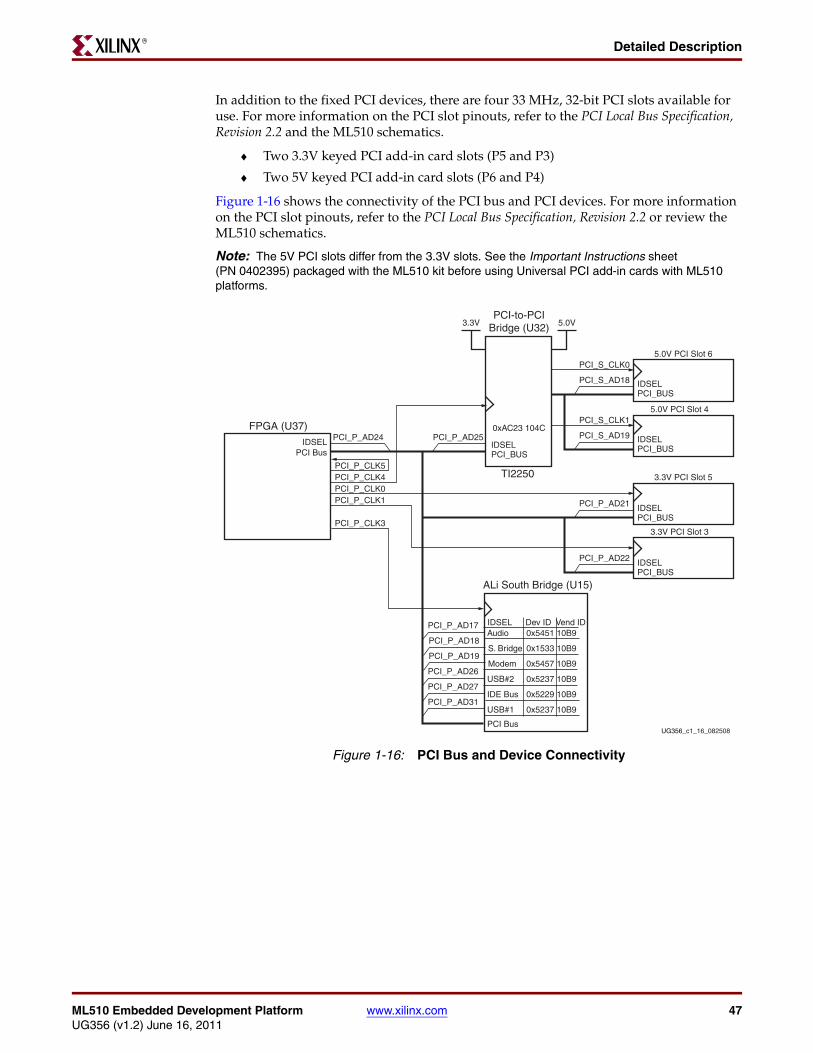
In addition to the fixed PCI devices, there are four 33 MHz, 32-bit PCI slots available for use. For more information on the PCI slot pinouts, refer to the PCI Local Bus Specification, Revision 2.2 and the ML510 schematics.
♦ Two 3.3V keyed PCI add-in card slots (P5 and P3)
♦ Two 5V keyed PCI add-in card slots (P6 and P4)
Figure 1-16 shows the connectivity of the PCI bus and PCI devices. For more information on the PCI slot pinouts, refer to the PCI Local Bus Specification, Revision 2.2 or review the ML510 schematics.
Note: The 5V PCI slots differ from the 3.3V slots. See the Important Instructions sheet (PN 0402395) packaged with the ML510 kit before using Universal PCI add-in cards with ML510 platforms.X-Ref Target - Figure 1-16
Figure 1-16: PCI Bus and Device Connectivity
PCI-to-PCIBridge (U32)
5.0V PCI Slot 6
5.0V PCI Slot 4
ALi South Bridge (U15)
IDSELIDSEL
0xAC23 104C
0x5451 10B9Dev ID Vend IDIDSEL
0x1533 10B9
0x5457 10B9
0x5237 10B9
0x5229 10B9
0x5237 10B9
PCI_BUS
IDSELPCI_BUS
IDSELPCI_BUS
IDSELPCI_BUS
IDSELPCI_BUS
USB#1
PCI Bus
PCI Bus
PCI_S_AD18
PCI_S_CLK0
PCI_S_AD19PCI_P_AD25PCI_P_AD24
3.3V
PCI_P_CLK5PCI_P_CLK4PCI_P_CLK0PCI_P_CLK1
PCI_P_CLK3
PCI_S_CLK1
3.3V PCI Slot 5
3.3V PCI Slot 3
PCI_P_AD21
PCI_P_AD22
PCI_P_AD31IDE Bus
PCI_P_AD27USB#2
PCI_P_AD26Modem
PCI_P_AD19S. Bridge
PCI_P_AD18Audio
PCI_P_AD17
5.0V
FPGA (U37)
UG356_c1_16_082508
TI2250

48 www.xilinx.com ML510 Embedded Development PlatformUG356 (v1.2) June 16, 2011
Chapter 1: ML510 Embedded Development PlatformR
Table 1-21 shows how the primary PCI bus interrupts are connected on ML510 platforms along with information for each device.
Table 1-22 shows how the secondary PCI bus interrupts are connected on ML510 platforms along with information for each device.
Table 1-21: 3.3V Primary PCI Bus Information
PCI Interrupts on FPGA
Device Name Dev. IDVend.
IDBus DEV IDSEL REQ
FPGAPCI CLK A B C D ALI SBR
PCI Slot 5 N/A N/A 0 5 AD21 0 0
PC
I Dev
ice
Inte
rru
pt
D A B C -
PCI Slot 3 N/A N/A 0 6 AD22 1 1 C D A B -
U15, ALi SB 0x1533 0x10B9 0 2 AD18 3 3 - - - - (INT, NMI)
U15, ALi Pwr Mgmt
0x7101 0x10B9 0 12 AD28 3 3 - - - - (INT, NMI)
U15, ALi IDE 0x5229 0x10B9 0 11 AD27 3 3 - - - - (INT, NMI)
U15, ALi Audio 0x5451 0x10B9 0 1 AD17 3 3 - - - - (INT, NMI)
U15, ALi Modem 0x5457 0x10B9 0 3 AD19 3 3 - - - - (INT, NMI)
U15, ALi USB#1 0x5237 0x10B9 0 15 AD31 3 3 - - - - (INT, NMI)
U15, ALi USB#2 0x5237 0x10B9 0 10 AD26 3 3 - - - - (INT, NMI)
U32, PCI-PCI Brg 0xAC23 0x104C 0 9 AD25 4 4 - - - - -
U37, FPGA 0x0410 0x10EE 0 8 AD24 Int. 5 - - - - -
Notes: The PCI ALi South Bridge device uses a separate interrupt line that connects to the FPGA via schematic net SBR_INTR. Anytime an interrupt occurs within the ALi South Bridge, it generates an interrupt on schematic net SBR_INTR.
Table 1-22: 5V Secondary PCI Bus Information
PCI Interrupts on FPGA
Device Name Dev. ID Vend. ID Bus DEV IDSEL REQBridge
CLK A B C D ALI SBR
PCI Slot 6 N/A N/A 1 2 AD18 0 0
PC
I Dev
. Int
r. B C D A -
PCI Slot 4 N/A N/A 1 3 AD19 1 1 A B C D -
U32, PCI-PCI Brg N/A N/A N/A 7 N/A Int. 4 - - - - -
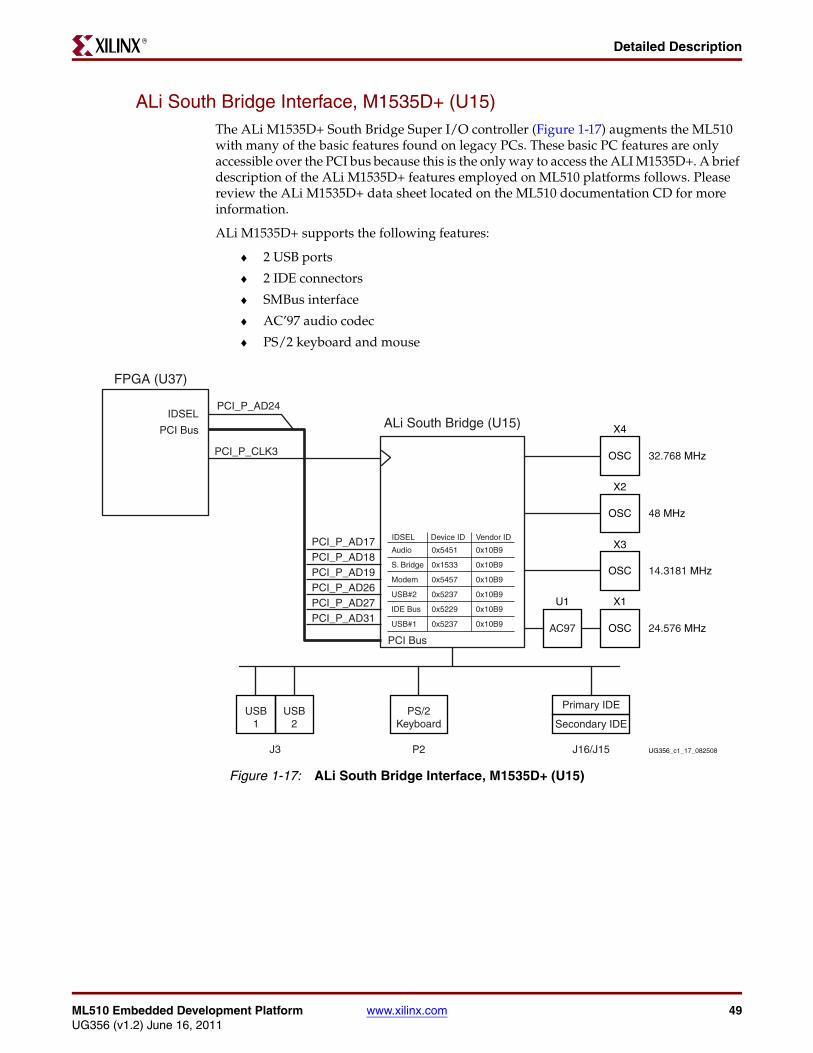
ML510 Embedded Development Platform www.xilinx.com 49UG356 (v1.2) June 16, 2011
Detailed DescriptionR
ALi South Bridge Interface, M1535D+ (U15)The ALi M1535D+ South Bridge Super I/O controller (Figure 1-17) augments the ML510 with many of the basic features found on legacy PCs. These basic PC features are only accessible over the PCI bus because this is the only way to access the ALI M1535D+. A brief description of the ALi M1535D+ features employed on ML510 platforms follows. Please review the ALi M1535D+ data sheet located on the ML510 documentation CD for more information.
ALi M1535D+ supports the following features:
♦ 2 USB ports
♦ 2 IDE connectors
♦ SMBus interface
♦ AC’97 audio codec
♦ PS/2 keyboard and mouse X-Ref Target - Figure 1-17
Figure 1-17: ALi South Bridge Interface, M1535D+ (U15)
PCI_P_AD31PCI_P_AD27PCI_P_AD26PCI_P_AD19PCI_P_AD18PCI_P_AD17
ALi South Bridge (U15)
AC97
PCI_P_AD24
PCI_P_CLK3
PCI Bus
IDSEL
FPGA (U37)
J3
PCI Bus
Device ID Vendor IDIDSEL
0x5451
0x1533
0x5457
0x5237
0x5229
0x5237
0x10B9
0x10B9
0x10B9
0x10B9
0x10B9
0x10B9USB#1
IDE Bus
USB#2
Modem
S. Bridge
Audio
UG356_c1_17_082508
X4
32.768 MHz
X2
48 MHz
X3
14.3181 MHz
X1
OSC
OSC
OSC
OSC 24.576 MHz
U1
USB1
USB2
P2
PS/2Keyboard
J16/J15
Primary IDE
Secondary IDE

50 www.xilinx.com ML510 Embedded Development PlatformUG356 (v1.2) June 16, 2011
Chapter 1: ML510 Embedded Development PlatformR
USB Connector Assembly (J3)
The M1535D+ USB is an implementation of the Universal Serial Bus Specification Version 1.0a (see www.usb.org) that contains two PCI Host Controllers and an integrated Root Hub. The two USB connectors, A/B, are part of the J3 connector assembly and are USB Type-A plugs.
Table 1-23 shows the ALi USB connections to the two USB Type-A plugs (J3).
IDE Connectors (J15 and J16)
Supports a two-channel UltraDMA-133 IDE master controller independently connected to a primary 40-pin IDE connector (J16) and a secondary 40-pin IDE connector (J15).
Table 1-24 shows the ALi Primary and Secondary IDE connections.
Table 1-23: ALi South Bridge Connections to USB Type-A
Signal Name A/B Pin (J3) Description
USB_VCC 1 USB Power, 5V, MOSFET Isolated
USB0_DN/USB1_DN 2 USB Data -
USB0_DP/USB1_DP 3 USB Data +
GND 4 Ground
Table 1-24: ALi South Bridge IDE Connections
IDE PrimaryPin (J16)
Schematic SignalIDE Secondary
Pin (J15)Schematic Signal
1 PIDE_RESET_B 1 SIDE_RESET_B
2 GND 2 GND
3 PIDE_D7 3 SIDE_D7
4 PIDE_D8 4 SIDE_D8
5 PIDE_D6 5 SIDE_D6
6 PIDE_D9 6 SIDE_D9
7 PIDE_D5 7 SIDE_D5
8 PIDE_D10 8 SIDE_D10
9 PIDE_D4 9 SIDE_D4
10 PIDE_D11 10 SIDE_D11
11 PIDE_D3 11 SIDE_D3
12 PIDE_D12 12 SIDE_D12
13 PIDE_D2 13 SIDE_D2
14 PIDE_D13 14 SIDE_D13
15 PIDE_D1 15 SIDE_D1
16 PIDE_D14 16 SIDE_D14
17 PIDE_D0 17 SIDE_D0
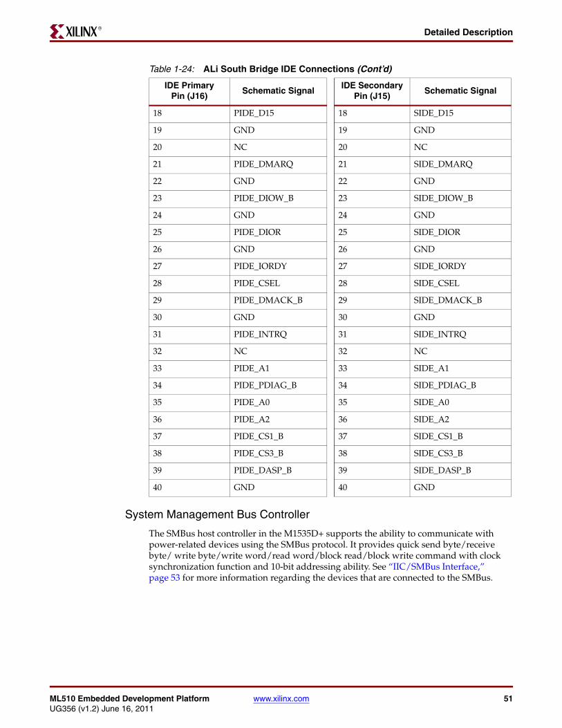
ML510 Embedded Development Platform www.xilinx.com 51UG356 (v1.2) June 16, 2011
Detailed DescriptionR
System Management Bus Controller
The SMBus host controller in the M1535D+ supports the ability to communicate with power-related devices using the SMBus protocol. It provides quick send byte/receive byte/ write byte/write word/read word/block read/block write command with clock synchronization function and 10-bit addressing ability. See “IIC/SMBus Interface,” page 53 for more information regarding the devices that are connected to the SMBus.
18 PIDE_D15 18 SIDE_D15
19 GND 19 GND
20 NC 20 NC
21 PIDE_DMARQ 21 SIDE_DMARQ
22 GND 22 GND
23 PIDE_DIOW_B 23 SIDE_DIOW_B
24 GND 24 GND
25 PIDE_DIOR 25 SIDE_DIOR
26 GND 26 GND
27 PIDE_IORDY 27 SIDE_IORDY
28 PIDE_CSEL 28 SIDE_CSEL
29 PIDE_DMACK_B 29 SIDE_DMACK_B
30 GND 30 GND
31 PIDE_INTRQ 31 SIDE_INTRQ
32 NC 32 NC
33 PIDE_A1 33 SIDE_A1
34 PIDE_PDIAG_B 34 SIDE_PDIAG_B
35 PIDE_A0 35 SIDE_A0
36 PIDE_A2 36 SIDE_A2
37 PIDE_CS1_B 37 SIDE_CS1_B
38 PIDE_CS3_B 38 SIDE_CS3_B
39 PIDE_DASP_B 39 SIDE_DASP_B
40 GND 40 GND
Table 1-24: ALi South Bridge IDE Connections (Cont’d)
IDE PrimaryPin (J16)
Schematic SignalIDE Secondary
Pin (J15)Schematic Signal

52 www.xilinx.com ML510 Embedded Development PlatformUG356 (v1.2) June 16, 2011
Chapter 1: ML510 Embedded Development PlatformR
AC’97 Audio Interface
The ALi South Bridge Super I/O controller has a built-in audio interface that is combined with a standard audio codec (AC’97), LM4550. Available features include:
♦ AC’97 Codec 2.1 Specification compliant
♦ Codec variable sample rate support
♦ 32-voice hardware wave-table synthesis
♦ 32 independent DMA channels
♦ 3D positioning sound acceleration
♦ Legacy Sound Blaster compatible
♦ FM OPL3 emulation
♦ MIDI interpretation
♦ MIDI MPU-401 interface
ML510 platforms employ a National Semiconductor LM4550 audio codec (U1) combined with the ALi South Bridge AC’97 interface. This interface can be used to play and record audio. The LM4550 has left and right channel line inputs, left and right CD-ROM inputs, a microphone input, left and right channel line outputs, and an amplified headphone output suitable for driving an 8Ω load using the LM4880 (U2). The microphone input and right/left amplified outputs are easily accessible via two 2.5 mm audio jacks on the J1 connector. The Line In and Line Out connections are accessible via two headers (J2 and J31).
Table 1-25 describes the audio jacks available to the user on ML510 platforms.
PS/2 Keyboard and Mouse Interface Connector (P2)
The ALi M1535D+ has a built-in PS2/AT keyboard and PS/2 mouse controller. The PS/2 keyboard and mouse ports are connected to the ALi M1535D+ through standard DIN connectors contained in the P2 connector assembly. In the event of a short circuit by the keyboard or mouse device, the 5V power provided to these devices is protected by a resettable fuse, F1.
Table 1-25: Audio Jacks (J1, J2, and J31)
Audio Jack Signal Name Description
J1 TopAC_AMP_OUTRAC_AMP_OUTL
AC Amplified Output, right and left channels,driven by U2, LM4880
J1 Bottom AC_MIC_IN Microphone Input to U1, LM4550
J31 AC_LINE_OUTRAC_LINE_OUTL
AC Line Output, right and left channels, driven by U1, LM4550
J2 AC_LINE_INRAC_LINE_INL
AC Line Input, right and left channels, driven by U1, LM4550
J6 AC_CD_INRAC_CD_INL
AC CD Input, right and left channels, driven by U1, LM4550

ML510 Embedded Development Platform www.xilinx.com 53UG356 (v1.2) June 16, 2011
Detailed DescriptionR
Table 1-26 shows the PS/2 keyboard and mouse connections to the P2 connector assembly.
IIC/SMBus Interface
Introduction to IIC/SMBus
The Inter Integrated Circuit (IIC) bus provides the connection from the CPU to peripherals. It is a serial bus with a data signal, SDA, and a clock signal, SCL, both of which are bidirectional. The IIC/SMBus interface serves as an interface to one master device and multiple slave devices. The interface operates in the range of 100 kHz to 400 kHz.
The SMBus also provides connectivity from the CPU to peripherals. The SMBus is also a two wire serial bus through which simple power related devices can communicate with the rest of the system. SMBus uses IIC as its backbone. EDK provides IP that integrates the IIC interface with a microprocessor system. See the Embedded Processor Block in Virtex-5 FPGAs Reference Guide [Ref 4] for more details.
IIC/SMBus Signaling
The IIC bus data and clock signals operate as open-drain. By default, these signals are pulled High to 3.3V, although some devices support lower voltages. Either the master device or a slave device can drive either of the signals Low to transmit data or clock signals.
IIC/SMBus
Table 1-27 lists the function, part number, and addresses of the IIC devices. These devices include EEPROM, temperature sensors, power monitors, and a Real Time Clock.
Table 1-26: PS/2 Keyboard and Mouse
Signal Name PS2 Pin (P2) Description
KDAT 1B Keyboard data
KCLK 5B Keyboard clock
MDAT 1C Mouse data
MCLK 5C Mouse clock
KVCC, MVCC 4B, 4C Fuse protected power to keyboard and mouse
Table 1-27: IIC and SMBus Controller Connections
Signal Name FPGA Pin (U37)
FPGA_SCL L7
FPGA_SDA K8
IIC_IRQ_B AK25
IIC_THERM_B(1) AN24
IIC_SDA_VIDEO M7
IIC_SCL_VIDEO L9
Notes: 1. This signal connects to U20 therm_l on the LM87. See data sheet
for additional details.

54 www.xilinx.com ML510 Embedded Development PlatformUG356 (v1.2) June 16, 2011
Chapter 1: ML510 Embedded Development PlatformR
Figure 1-18 shows a block diagram of the FPGA in relation to the SMBus accelerator and the IIC bus.
Note: Either the FPGA or the ALi M1535D+ can master the IIC bus, but not simultaneously. X-Ref Target - Figure 1-18
Figure 1-18: IIC and SMBus Block Diagram
FPGA (U37)
ALi South Bridge(U15)
M1535 D+
U27
SMBusAcceleratorLTC1694
ADDR:0x5C
ADDR:0xA2
Real Time Clock
ADDR:0xA0
EEPROM
SPD EEPROMDIMM0 ADDR:
VoltageTemp
Monitor
Temperature
U20
LM87
VCC12V_P
VCC5V
VCC2V5
VVCC3_PCI
VCC1V2
Write Protect (Jumper Off)
IIC Bus (Main)
PCI Bus
U22
RTC8564
Front PanelHeader
J23
U21
24LC64
ADDR:0x8E
MIC2592BPCIe Pwr Ctlr
U55
U59
P48
P9
P10
Note: Located on DDR2 DIMM P48
UG356_c1_18_082508
0xA8
SPD EEPROMDIMM1 ADDR:
0xA6
DVI CH7301CADDR: DVI Connector
0x76
IIC Bus (Video)
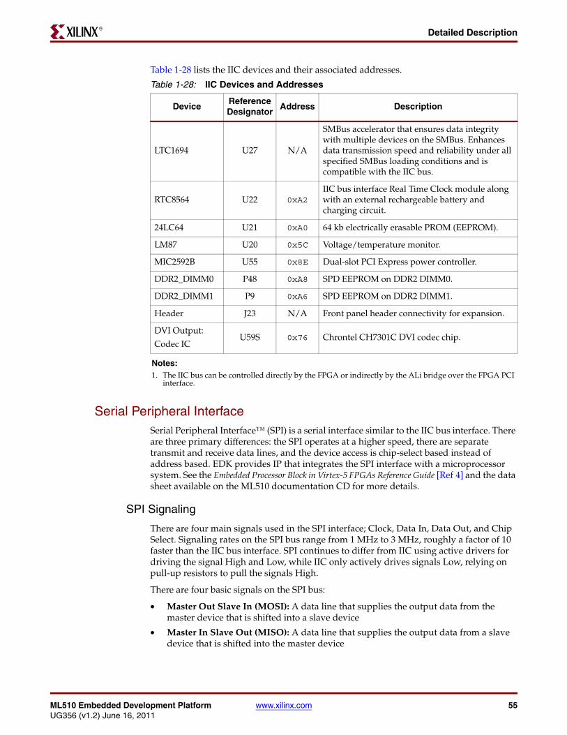
ML510 Embedded Development Platform www.xilinx.com 55UG356 (v1.2) June 16, 2011
Detailed DescriptionR
Table 1-28 lists the IIC devices and their associated addresses.
Serial Peripheral InterfaceSerial Peripheral Interface™ (SPI) is a serial interface similar to the IIC bus interface. There are three primary differences: the SPI operates at a higher speed, there are separate transmit and receive data lines, and the device access is chip-select based instead of address based. EDK provides IP that integrates the SPI interface with a microprocessor system. See the Embedded Processor Block in Virtex-5 FPGAs Reference Guide [Ref 4] and the data sheet available on the ML510 documentation CD for more details.
SPI Signaling
There are four main signals used in the SPI interface; Clock, Data In, Data Out, and Chip Select. Signaling rates on the SPI bus range from 1 MHz to 3 MHz, roughly a factor of 10 faster than the IIC bus interface. SPI continues to differ from IIC using active drivers for driving the signal High and Low, while IIC only actively drives signals Low, relying on pull-up resistors to pull the signals High.
There are four basic signals on the SPI bus:
• Master Out Slave In (MOSI): A data line that supplies the output data from the master device that is shifted into a slave device
• Master In Slave Out (MISO): A data line that supplies the output data from a slave device that is shifted into the master device
Table 1-28: IIC Devices and Addresses
DeviceReference Designator
Address Description
LTC1694 U27 N/A
SMBus accelerator that ensures data integrity with multiple devices on the SMBus. Enhances data transmission speed and reliability under all specified SMBus loading conditions and is compatible with the IIC bus.
RTC8564 U22 0xA2IIC bus interface Real Time Clock module along with an external rechargeable battery and charging circuit.
24LC64 U21 0xA0 64 kb electrically erasable PROM (EEPROM).
LM87 U20 0x5C Voltage/temperature monitor.
MIC2592B U55 0x8E Dual-slot PCI Express power controller.
DDR2_DIMM0 P48 0xA8 SPD EEPROM on DDR2 DIMM0.
DDR2_DIMM1 P9 0xA6 SPD EEPROM on DDR2 DIMM1.
Header J23 N/A Front panel header connectivity for expansion.
DVI Output:
Codec ICU59S 0x76 Chrontel CH7301C DVI codec chip.
Notes: 1. The IIC bus can be controlled directly by the FPGA or indirectly by the ALi bridge over the FPGA PCI
interface.
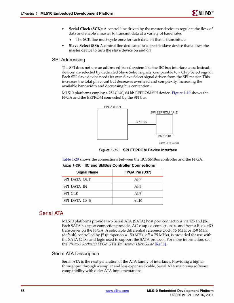
56 www.xilinx.com ML510 Embedded Development PlatformUG356 (v1.2) June 16, 2011
Chapter 1: ML510 Embedded Development PlatformR
• Serial Clock (SCK): A control line driven by the master device to regulate the flow of data and enable a master to transmit data at a variety of baud rates
♦ The SCK line must cycle once for each data bit that is transmitted
• Slave Select (SS): A control line dedicated to a specific slave device that allows the master device to turn the slave device on and off
SPI Addressing
The SPI does not use an addressed-based system like the IIC bus interface uses. Instead, devices are selected by dedicated Slave Select signals, comparable to a Chip Select signal. Each SPI slave device needs its own Slave Select signal driven from the SPI master. This increases the total pin count but decreases overhead and complexity, increasing the available bandwidth and decreasing bus contention.
ML510 platforms employ a 25LC640, 64 kb EEPROM SPI device. Figure 1-19 shows the FPGA and the EEPROM connected by the SPI bus.
Table 1-29 shows the connections between the IIC/SMBus controller and the FPGA.
Serial ATAML510 platforms provide two Serial ATA (SATA) host port connections via J25 and J26. Each SATA host port connection provides AC-coupled connections to and from a RocketIO transceiver on the FPGA. A selectable differential reference clock, 75 MHz or 150 MHz (default) controlled by J5 (jumper on = 150 MHz; off = 75 MHz), is provided for use with the SATA GTXs and logic used to support the SATA protocol. For more information, see the Virtex-5 RocketIO FPGA GTX Transceiver User Guide [Ref 5].
Serial ATA Description
Serial ATA is the next generation of the ATA family of interfaces. Providing a higher throughput through a simpler and less expensive cable, Serial ATA maintains software compatibility with older ATA implementations.
X-Ref Target - Figure 1-19
Figure 1-19: SPI EEPROM Device Interface
Table 1-29: IIC and SMBus Controller Connections
Signal Name FPGA Pin (U37)
SPI_DATA_OUT AP7
SPI_DATA_IN AP5
SPI_CLK AL9
SPI_DATA_CS_B AL10
FPGA (U37)
SPI EEPROM (U19)
25LC640
SPI Bus
UG356_c1_19_082508
ML510 Embedded Development Platform www.xilinx.com 57UG356 (v1.2) June 16, 2011
Detailed DescriptionR
FPGA to Serial ATA Connector
ML510 platforms that are equipped with RocketIO transceivers provide for operation as a Serial ATA host or device. These connections are also shown in Table 1-30.
The Serial ATA connectors have different connections to the FPGA for transmit and receive differential pairs. The receive differential pair is connected by way of a 0.01 µF capacitor to AC-couple the incoming signal to the FPGA. The transmit differential pair between the FPGA and the Serial ATA connector is connected by way of a 0Ω resistor. The resistor is a place holder to allow for AC-coupling if required at a future date.
Pushbuttons, Switches, Front Panel Interface, and Jumpers
Pushbuttons
System ACE Reset (SW1)
SW1 is a manual reset switch for the System ACE CF (U38) device. When SW1 is actuated, it drives the PB_SYSTEM_ACE_RESET signal Low, which causes the LTC1326 (U31) to generate a 100 µs active-Low pulse. The active-Low output from the LTC1326 drives the reset input of the System ACE CF controller (U38) through the SYSTEMACE_RESET_N signal. When the System ACE CF device is reset, it causes the FPGA to be reconfigured. The ACE file that is used to program the device is selected via SW3 DIP switch settings.
Note: The System ACE configuration address lines, CFG[0:1], are shared with the upper address lines of the BPI flash device. Because these connections are shared, before manually moving to a different System ACE configuration file the user must first pulse the PROG pushbutton before pulsing the System ACE Reset pushbutton. This is required only when the user has implemented a design that drives the flash address lines, such as the EDK EMC controller.
The front panel interface header (J23) can also drive the PB_SYSTEM_ACE_RESET signal. For more details on J23, see the “Front Panel Interface (J23)” section.
Table 1-30: Connections Between FPGA and Serial ATA Connector (J25 and J26)
Signal Name FPGA Pin (U37) Serial ATA Pin
GTP_120_RX0_N F1 J26.3
GTP_120_RX0_N E1 J26.2
GTP_120_TX0_N E2 J26.5
GTP_120_TX0_N D2 J26.6
GTP_120_RX1_N G1 J25.3
GTP_120_RX1_N H1 J25.2
GTP_120_TX1_N H2 J25.5
GTP_120_TX1_N J2 J25.6
SATACLK_Q0P(1) F4 -
SATACLK_Q0N(1) F3 -
Notes: 1. 75/150 MHz

58 www.xilinx.com ML510 Embedded Development PlatformUG356 (v1.2) June 16, 2011
Chapter 1: ML510 Embedded Development PlatformR
CPU Reset (SW2)
SW2 is a manual pushbutton reset switch for the PPC440 system implemented in the FPGA. To use this switch, the user must connect the PB_FPGA_CPU_RESET signal to the PPC440 system within the FPGA fabric. EDK provides IP to perform this task. See the Embedded Processor Block in Virtex-5 FPGAs Reference Guide [Ref 4] for more details.
If the SW2 switch is connected in the FPGA fabric, it drives the PB_FPGA_CPU_RESET signal Low when pushed, causing the LTC1326 (U30) to generate a 100 µs active-Low pulse. The active-Low output of the LTC1326 pin drives the FPGA_CPU_RESET_N signal connected to J15 on the FPGA.
In addition to resetting the CPU, SW2 can also perform a System ACE CF reset as described in “System ACE Reset (SW1),” page 57. This can be accomplished by simply holding down the SW2 pushbutton for longer than two seconds. This action performs a CPU reset followed by a System ACE CF reset. See the ML510 schematics and the LTC1236 data sheet on the ML510 documentation CD for more details.
The front panel interface header (J23) can also drive the PB_ FPGA_CPU_RESET signal. For more details on J23, please review the “Front Panel Interface (J23)” section.
FPGA Prog (SW4)
SW4 is a pushbutton switch that grounds the FPGA Prog pin when pressed. This action clears the FPGA configuration.
Switches
Configuration Control (SW3)
The Configuration control DIP switch, SW3, controls the selection of the different configuration modes available on the ML510 board. The ML510 supports the following configuration options; JTAG, System ACE CompactFlash memory, and Linear BPI flash. Refer to “Configuration Options,” page 77 for more details.
Front Panel Interface (J23)
The front panel interface connector (J23) is a 24-pin header that accepts a standard IDC 24 pin connector (0.1 inch pitch). J23 provides an optional means to control and gather status information from the ML510 if enclosed in a case similar to a desktop computer. The functionality listed below can easily be connected with a custom user-provided cable that connects to user logic designed to control and monitor the functionality available through the front panel interface.
The front panel interface provides the following control capability:
♦ Power ON|OFF the board
- ML510 platforms are delivered with a jumper installed on J23
♦ Eight System ACE configuration selections
- Connects to the three System ACE configuration address lines
♦ System ACE Reset
- Active-Low input (pulsed)
♦ CPU Reset
- Active-Low input (pulsed)
The front panel interface provides access to the following status information:
ML510 Embedded Development Platform www.xilinx.com 59UG356 (v1.2) June 16, 2011
Detailed DescriptionR
♦ FPGA configuration DONE output
♦ IDE disk access output
♦ ATX power output
♦ Two FPGA user-defined output signals
♦ ATX speaker output
♦ Keyboard inhibit input (active-Low)
Note: All front panel interface outputs, except for the speaker out, can drive LEDs.
Table 1-31 shows the signals available at the front panel interface header (J23).
Table 1-31: Front Panel Interface Connector (J23)
J23Pin
Schematic Signal Description
1 SYACE_CFGA0 Used to select System ACE configuration, CFGADDR0
2 FPGA_LED_USER1User defined function, connects to the FPGA, U37-G15, (2.5V )
3 SYACE_CFGA1 Used to select System ACE configuration, CFGADDR1
4 FPGA_LED_USER2User defined function, connects to the FPGA, U37-G16, (2.5V )
5 SYACE_CFGA2 Used to select System ACE configuration, CFGADDR2
6 NC No Connect
7 LED_DONE_RRemote FPGA DONE indicator; tie this pin to anode of user’s LED and cathode to ground
8 GND Ground
9 ATX_PWRLEDATX 3.3V power indicator; tie this pin to anode of user’s LED and cathode to ground
10 ATX_SPKR Used to drive user-provided ATX speaker
11 SCL IIC bus
12 SCA IIC bus
13 GND Ground
14 GND Ground
15 KBINHTie this pin to ground to activate Keyboard Inhibit (See ALi M1536D+ data sheet for more details)
16 VCC5V 5V ATX power available to user
17 ATX_IDELED_RATX IDE access indicator; tie this pin to anode of user’s LED and cathode to ground
18 VCC5V 5V ATX power available to user
19 GND Ground
20 PWR_SUPPLY_ONJumper J20 to J19 (GND) allows the ATX power supply AC switch to control power-on of the board. Removing the jumper prevents the ATX supply from powering on.
60 www.xilinx.com ML510 Embedded Development PlatformUG356 (v1.2) June 16, 2011
Chapter 1: ML510 Embedded Development PlatformR
Jumpers
Note: Pins should only be jumpered with the board powered off.
12V Fan (J7)
Table 1-32 shows the pinout of the 5V fan.
5V Fan (J8)
Table 1-33 shows the pinout of the 5V fan.
JTAG Source Select
The JTAG source select, SW3 position 7, enables the use of either the PC4 JTAG connector (J9) or the CPU JTAG (J12) and FPGA JTAG/TRACE (P8) to source the FPGA JTAG pins. This is available for third-party tool support. The multiplexing is performed by an external device, 74LVC157A (U39), as shown in Figure 1-9.
Note: To avoid contention after the FPGA is configured, this functionality should not be used if logic that also drives the CPU JTAG connector (J12) or the FPGA JTAG/TRACE connector (P8) is implemented.
21 PB_SYSACE_RESETUsed to reset System ACE when driven Low, as described in “System ACE Reset (SW1)”
22 GND Ground
23 PB_FPGA_CPU_RESETUsed to reset CPU when driven Low, as described in “CPU Reset (SW2)”
24 GND Ground
Table 1-31: Front Panel Interface Connector (J23) (Cont’d)
J23Pin
Schematic Signal Description
Table 1-32: 12V Fan Header Connections
J7Pin
Description
1 +12V
2 Ground
3 Fan Tachometer
Table 1-33: 5V Fan Header Connections
J8Pin
Description
1 +5V
2 Ground
ML510 Embedded Development Platform www.xilinx.com 61UG356 (v1.2) June 16, 2011
Detailed DescriptionR
I/O Voltage Margining (J24 and J37)
The voltage margins on the board can be adjusted by shorting the jumpers as shown in Table 1-34. Apply shorting jumpers only when the board is powered off. For more on voltage regulation, see “ATX Power Distribution and Voltage Regulation.”
Table 1-34: Voltage Margining Jumper Settings
Voltage Regulator
Inhibit Jumper(1)
Margin Jumper
Description
VR1 J30 J24
To adjust the 2.5V supply:
• Equal to or greater than –5% margining, short pins 1–2 on J34
• Equal to or greater than +5% margining, short pins 2–3 on J34
• No margining, leave pins open on J34
VR2 - - No margining available on the 1.0V supply
VR3 J35 J37
To adjust the 2.0V supply:
• Equal to or greater than –5% margining, short pins 1–2
• Equal to or greater than +5% margining, short pins 2–3
• No margining, leave pins open
Notes: 1. Inhibit jumpers are open by default at nominal voltage.

62 www.xilinx.com ML510 Embedded Development PlatformUG356 (v1.2) June 16, 2011
Chapter 1: ML510 Embedded Development PlatformR
ATX Power Distribution and Voltage RegulationML510 platforms are shipped with a commercially available 250 W ATX power supply. All voltages required by the ML510 logic devices are derived from the 5V supply, except the ±12V supplies, as shown in Figure 1-20. The ATX power supply can be easily mounted in a standard ATX chassis along with the ML510 board.
The ATX power supply is a Sparkle Power Inc. model FSP250-60PLN. The Sparkle User’s Manual is provided in the data sheet section on the ML510 documentation CD. The Sparkle power supply supports a full range input to automatically accommodate a wide range of voltage/frequency standards, such as 115V for North America, Japan, and others, and 230V for most European countries. See the Sparkle User’s Manual for more information.
The different logic devices used on the ML510 platforms require a variety of voltages. Voltage levels are derived from the 5V supply and regulated on the board as shown in Figure 1-20.X-Ref Target - Figure 1-20
Figure 1-20: ATX Power Distribution and Voltage Regulation
DVI_VACC
U41
LT1736
U56
TPS51116
VR1
PTH05010
VR2
PTH05T210W
VR3
PTH05010
VCC5V VCC3V_PCI
AC_VDD
VCC1V8VTT_DDR2
VCC2V5
VCC1V0
VCC2V0 Q6MAX8556
Q7MAX8556
Q8MAX8556
Q9MAX8556
2.5V@15A
1.0V@30A
2.0V@15A
GTP=1.2V@4AGTX=1.0V@4A
1.0V@4A
1.2V@4A
1.2V@4A
GTP/GTX_AVCC_PLL
GTP_AVCC
GTP_AVTTRX
GTP_AVTTTX
U3
LT1763
VCC12V_P
J18VCC12V_P
VCC12V_N
VCC3V3
5V_STBY
VCC5VU44
LT1763
5V_STBY
3.3V@500mA
U10REF2912
U25TPS73633
MGTVREF
3.0V@500mA
5.0V@500mA
VREF_DDR20.9V@10mA
3.3@400mA
3V3_STBY
ATX
PW
R C
ON
UG356_c1_20_082508

ML510 Embedded Development Platform www.xilinx.com 63UG356 (v1.2) June 16, 2011
Detailed DescriptionR
Voltage monitors connected to power indicator LEDs monitor the regulated power on the board (see Figure 1-21). The indicator LEDs illuminate red if a regulated supply voltage is out of spec, and illuminate green if the regulated supply voltage is nominal. Each regulated supply voltage has a corresponding test point located near its indicator LED. See the ML510 schematics and the associated data sheets for more information.
In addition to the voltage monitors, the ML510 employs a SMBus device, LM87, which samples several of the same supply voltages when accessed over the System Management Bus. See the “IIC/SMBus Interface” section for more information. X-Ref Target - Figure 1-21
Figure 1-21: Voltage Monitors
UG356_c1_21_082508
U5
LTC1326
VCC1V0 VCC5V
GRN = Nominal
RED = Fault
TP17
U24
MC34161D
VCC2V5 VCC5V
GRN = Nominal
RED = Fault
TP14
U18
MC34161D
VCC3_PCI VCC5V
GRN = Nominal
RED = Fault
TP10
U13
MC34161D
VCC3V3 VCC5V
GRN = Nominal
RED = Fault
TP8
U28
MC34161D
VCC5V VCC5V
GRN = Nominal
RED = Fault
TP16
U23
NCP300
VTT_DDR2 VCC5V
GRN = Nominal
RED = Fault
TP13
U12
MC34161D
VCC1V8 VCC5V
GRN = Nominal
RED = Fault
U17
MC34161D
AVCCAUXMGT VCC5V
GRN = Nominal
RED = Fault
DS8
DS6
`
DS4
DS2
DS7
DS5
DS3
DS1
3.3V
3.0V
2.5V
1.0V 5.0V
0.9V
TP9
2.5V
TP7
1.8V
64 www.xilinx.com ML510 Embedded Development PlatformUG356 (v1.2) June 16, 2011
Chapter 1: ML510 Embedded Development PlatformR
Table 1-35 shows the various voltage monitor information.
System MonitorThe ML510 supports the dedicated analog inputs to the Virtex-5 FPGA System Monitor block. The VP and VN pins shown in Table 1-36, page 65 are the dedicated pins, whereas the VAUXP[x], VAUXN[x] 16 user-selectable auxiliary analog input channels are not supported as these pins are dedicated for use by the DDR2 memory interfaces. The ML510 PCB layout for the VP and VN pins is designed using differential pairs and anti-alias filtering in close proximity to the FPGA as recommended in the Virtex-5 FPGA System Monitor User Guide [Ref 10].
The Virtex-5 FPGA System Monitor function is built around a 10-bit, 200-kSPS (kilosamples per second) Analog-to-Digital Converter (ADC). When combined with a number of on-chip sensors, the ADC is used to measure FPGA physical operating parameters like on-chip power supply voltages and die temperatures. Access to external voltages is provided through a dedicated analog-input pair (VP/VN).
The System Monitor is fully functional on power up, and measurement data can be accessed via the JTAG port pre-configuration. The Xilinx ChipScope™ Pro tool [Ref 18] provides access to the System Monitor over the JTAG port. The System Monitor control logic implements some common monitoring features. For example, an automatic channel sequencer allows a user-defined selection of parameters to be automatically monitored, and user-programmable averaging is enabled to ensure robust noise-free measurements.
The System Monitor also provides user programmable alarm thresholds for the on-chip sensors. Thus, if an on-chip monitored parameter moves outside the user-specified operating range, an alarm logic output becomes active. In addition to monitoring the on-chip temperature for user-defined applications, the System Monitor issues a special alarm
Table 1-35: Voltage Monitor Information
Schematic Net Name
VoltageTest Point
Indicator LED(1) Description
VCC1V0 1.0V TP17 DS8 Regulated FPGA core voltage
VCC1V8 1.8V TP7 DS1 Regulated DDR2 power
VCC2V5 2.5V TP14 DS6 Regulated FPGA/board logic and DDR power
VCC3_PCI 3.0V TP10 DS4 Regulated FPGA PCI bank 1-2 voltage
VCC3V3 3.3V TP8 DS2 Regulated PCI and other logic
VCC5V 5V TP16 DS7 From ATX power supply, all regulators derive power
VTT_DDR2 0.9V TP13 DS5 Regulated DDR2 termination (SSTL18)
VTTDDR 1.25V Regulated DDR termination (SSTL2)
AVCCAUXMGT 2.5V TP9 DS3 Regulated RocketIO transceiver power
VCC12V_P +12V TP18 N/A Direct from ATX power supply
VCC12V_N –12V TP19 N/A Direct from ATX power supply
Notes: 1. Green LED = Voltage Nominal; Red LED = Voltage Fault

ML510 Embedded Development Platform www.xilinx.com 65UG356 (v1.2) June 16, 2011
Detailed DescriptionR
called Over-Temperature (OT) if the FPGA temperature becomes critical (> 125°C). The OT signal is deactivated when the device temperature falls below a user specified lower limit. If the FPGA power-down feature is enabled, the FPGA enters power down when the OT signal becomes active. The FPGA powers up again when the alarm is deactivated.
For additional information about the System Monitor, see http://www.xilinx.com/systemmonitor and consult the Virtex-5 FPGA System Monitor User Guide [Ref 10]. Table 1-36 shows the System Monitor connections (J33).
The ML510 supports the measurement of the output current of the FPGA’s VCCINT supply (Figure 1-22). The output of the VCCINT regulator is connected to a series 3W, 1%, 2.2 mΩ Kelvin resistor. The sense pin on the VCCINT regulator is connected to the FPGA (load) side of the Kelvin resistor in order to compensate for the voltage drop across the Kelvin resistor, as the FPGA current consumption varies. The voltage across the Kelvin resistor can be measured at the System Monitor header, J33. The Virtex-5 FPGA System Monitor supports measuring the voltage across the Kelvin resistor by jumpering J33 pins 10 and 12 and J33 pins 9 and 11. The VCCINT current can be calculated by using Ohms Law. X-Ref Target - Figure 1-22
Figure 1-22: Power Regulation and Measurement
Table 1-36: System Monitor Header (J33)
J33Pin
Schematic Signal Description
1 SMB_DX_PTemperature diode connection to LM87, anode connection. The LM87 is an IIC accessible device.(1)
2 FPGA_DX_PTemperature diode connection to FPGA, annode connection.(1)
3 SMB_DX_NTemperature diode connection to LM87, cathode connection. The LM87 is an IIC accessible device.(1)
4 FPGA_DX_NTemperature diode connection to FPGA, cathode connection.(1)
UG356_c1_30_102408
VCCINT 30ASwitching Regulator Kelvin Resistor
J33
CURRENT_SENSE_REG
VN
VP
DXN
DXP
CURRENT_SENSE_OUT
GND GND
+5V
FPGA 1
3
5
7
9
11
2
4
6
8
10
12
ADR_VREFP TEST_MON_AVDD
SMB_DX_P
SMB_DX_N
66 www.xilinx.com ML510 Embedded Development PlatformUG356 (v1.2) June 16, 2011
Chapter 1: ML510 Embedded Development PlatformR
High-Speed I/OThe ML510 platform’s high-speed I/O is based on the RocketIO transceiver and LVDS capability of Virtex-5 FXT FPGAs. The ML510 platform RocketIO signal integrity was engineered to meet typical data channel characteristics and may not be representative of the highest performance that can be achieved. The ML52x series of Virtex-5 FXT RocketIO Characterization Platforms should be used for detailed RocketIO transceiver link analysis.
The high-speed I/O signals on the FPGA are accessible through two personality module (PM) connectors, referred to as Personality Module 1 and Personality Module 2, on the ML510 platforms. The PM connectors are Tyco Z-Dok+ docking connectors. See the 1367550-5 data sheet at Tyco’s website (www.z-dok.com).
The ML510 is the host board, functioning as the development platform for the Virtex-5 FXT FPGA. The PM connectors on the ML510 platforms provide a means for extending the functionality of the board through high-speed I/O pins.
Figure 1-23 shows an example of a personality module connected to an embedded development platform (an ML310 in this example). The plug, located on the embedded
5 GND Ground
6 GND Ground
7 ADR_VREFP VREFP supply
8 TEST_MON_AVDD VDD from FPGA
9 TEST_MON_VN0_N Dedicated FPGA analog input pair (VP/VN) for access to external voltages.(2)
10 TEST_MON_VN0_P
11 CURRENT_SENSE_OUTTap used to measure current with ohm meter or System Monitor when jumpered correctly.(2) Negative side connection to the Kelvin resistor.
12 CURRENT_SENSE_REGTap used to measure current with ohm meter when jumpered correctly.(2) Positive side connection to the Kelvin resistor.
Notes: 1. Default setting = jumper over pins 1-2 and 3-4.2. To measure VCCINT current using the Virtex-5 FPGA System Monitor, jumper over pins 9-11 and 10-12.
Table 1-36: System Monitor Header (J33) (Cont’d)
J33Pin
Schematic Signal Description

ML510 Embedded Development Platform www.xilinx.com 67UG356 (v1.2) June 16, 2011
High-Speed I/OR
development platform, is referred to as the host board connector; the receptacle, located on the personality module, is referred to as the adapter board connector.
Personality Module ConnectorsFigure 1-24 shows an edge view of the PM host board connectors.
Each signal pair on the PM1 and PM2 host board connectors has a wide ground pin on the opposite side of the plastic divider, as shown in Figure 1-25. The signal pairs alternate from
X-Ref Target - Figure 1-23
Figure 1-23: Personality Module Connected to Embedded Development Platform
Host Board ConnectorAdapter Board Connector
PM1
PM2
Personality Module ML310 BoardUG356_c1_22_082508
X-Ref Target - Figure 1-24
Figure 1-24: Edge View of Host Board Connectors
PM1 Host Board Connector
PM2 Host Board ConnectorUG356_c1_23_082508
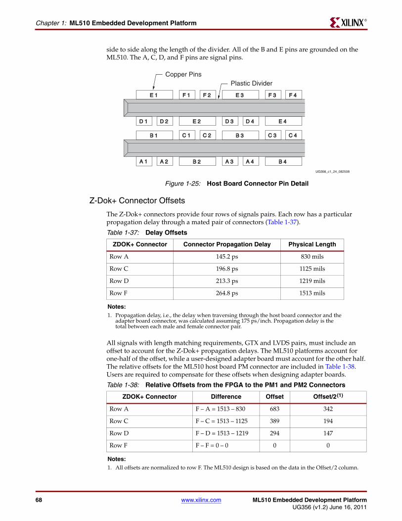
68 www.xilinx.com ML510 Embedded Development PlatformUG356 (v1.2) June 16, 2011
Chapter 1: ML510 Embedded Development PlatformR
side to side along the length of the divider. All of the B and E pins are grounded on the ML510. The A, C, D, and F pins are signal pins.
Z-Dok+ Connector Offsets
The Z-Dok+ connectors provide four rows of signals pairs. Each row has a particular propagation delay through a mated pair of connectors (Table 1-37).
All signals with length matching requirements, GTX and LVDS pairs, must include an offset to account for the Z-Dok+ propagation delays. The ML510 platforms account for one-half of the offset, while a user-designed adapter board must account for the other half. The relative offsets for the ML510 host board PM connector are included in Table 1-38. Users are required to compensate for these offsets when designing adapter boards.
X-Ref Target - Figure 1-25
Figure 1-25: Host Board Connector Pin Detail
Plastic DividerCopper Pins
D 2D 2D 1D 1 E 2E 2 D 4D 4D 3D 3 E 4E 4
B 1B 1 C 2C 2C 1C 1 B 3B 3 C 4C 4C 3C 3
A 2A 2A 1A 1 B 2B 2 A 4A 4A 3A 3 B 4B 4
E 1E 1 F 2F 2F 1F 1 E 3E 3 F 4F 4F 3F 3
UG356_c1_24_082508
Table 1-37: Delay Offsets
ZDOK+ Connector Connector Propagation Delay Physical Length
Row A 145.2 ps 830 mils
Row C 196.8 ps 1125 mils
Row D 213.3 ps 1219 mils
Row F 264.8 ps 1513 mils
Notes: 1. Propagation delay, i.e., the delay when traversing through the host board connector and the
adapter board connector, was calculated assuming 175 ps/inch. Propagation delay is the total between each male and female connector pair.
Table 1-38: Relative Offsets from the FPGA to the PM1 and PM2 Connectors
ZDOK+ Connector Difference Offset Offset/2(1)
Row A F – A = 1513 – 830 683 342
Row C F – C = 1513 – 1125 389 194
Row D F – D = 1513 – 1219 294 147
Row F F – F = 0 – 0 0 0
Notes: 1. All offsets are normalized to row F. The ML510 design is based on the data in the Offset/2 column.
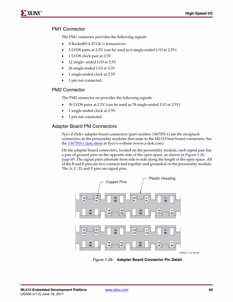
ML510 Embedded Development Platform www.xilinx.com 69UG356 (v1.2) June 16, 2011
High-Speed I/OR
PM1 Connector
The PM1 connector provides the following signals:
• 8 RocketIO 4.25 Gb/s transceivers
• 3 LVDS pairs at 2.5V (can be used as 6 single-ended I/O at 2.5V)
• 1 LVDS clock pair at 2.5V
• 12 single- ended I/O at 2.5V
• 26 single-ended I/O at 3.3V
• 1 single-ended clock at 2.5V
• 1 pin not connected
PM2 Connector
The PM2 connector on provides the following signals:
• 39 LVDS pairs at 2.5V (can be used as 78 single-ended I/O at 2.5V)
• 1 single-ended clock at 2.5V
• 1 pin not connected
Adapter Board PM Connectors
Tyco Z-Dok+ adapter board connectors (part number 1367555-1) are the receptacle connectors on the personality modules that mate to the ML510 host board connectors. See the 1367555-1 data sheet at Tyco’s website (www.z-dok.com).
On the adapter board connectors, located on the personality module, each signal pair has a pair of ground pins on the opposite side of the open space, as shown in Figure 1-26, page 69. The signal pairs alternate from side to side along the length of the open space. All of the B and E pins are two contacts tied together and grounded on the personality module. The A, C, D, and F pins are signal pins. X-Ref Target - Figure 1-26
Figure 1-26: Adapter Board Connector Pin Detail
B1
B1
C2
C2
C1
C1
B3
B3
C4
C4
C3
C3
A2
A2
A1
A1
B2
B2
A4
A4
A3
A3
B4
B4
E1
E1
F2
F2
F1
F1
E3
E3
F4
F4
F3
F3
D2
D2
D1
D1
E2
E2
D4
D4
D3
D3
E4
E4
Plastic HousingCopper Pins
UG356_c1_25_082508

70 www.xilinx.com ML510 Embedded Development PlatformUG356 (v1.2) June 16, 2011
Chapter 1: ML510 Embedded Development PlatformR
Z-DOK+ Utility PinsFigure 1-27 shows the Z-DOK+ utility pins and numbering for the host board PM connector.
Figure 1-28 shows the Z-DOK+ utility pins and numbering for the adapter board connector.
Note: The pins on the adapter board connector are at varying heights, as shown in Table 1-39 and Table 1-40, page 71.
Contact Order
The Z-Dok+ power and ground pins contact in the following order:
• 1 and 6;
• then 2 and 5;
• then 3 and 4
X-Ref Target - Figure 1-27
Figure 1-27: Z-DOK+ Utility Pins (ML510 Side)
X-Ref Target - Figure 1-28
Figure 1-28: Z-DOK+ Utility Pins (Adapter Side)
6 5 4 3 2 1
UG356_c1_26_082508
1 2 3 4 65
UG356_c1_27_082508
ML510 Embedded Development Platform www.xilinx.com 71UG356 (v1.2) June 16, 2011
High-Speed I/OR
PM1 Power and Ground
Table 1-39 shows the power and ground pins for the PM1 connector on the ML510.
PM User I/O Pins
PM1 User I/O
The PM1 connector makes the GTX signals from the eight RocketIO transceivers available to the user, along with LVDS pairs and single-ended signals. Table 1-40 shows the pinout for the PM1 connector.
Table 1-39: PM1 Power and Ground Pins
Pin Number Description Length Contact Order
1, 6 Ground Level 4 First
2, 5 2.5V Level 3 Second
3 3.3V Level 2 Third
4 1.2V Level 2 Third
Table 1-40: PM1 Pinout
PM1 Pin FPGA Pin Signal Name FPGA Bank
VCCOPin Function
A1 AV33 PM_IO_94_P 2.5V Single-ended 50Ω impedance
A2 AV34 PM_IO_95_N 2.5V Single-ended 50Ω impedance
A3 AU36 PM_IO_86_P 2.5V Single-ended 50Ω impedance
A4 AT35 PM_IO_87_N 2.5V Single-ended 50Ω impedance
A5 V6 PM_IO_3V_25_N 3V Single-ended 50Ω impedance
A6 V5 PM_IO_3V_18_P 3V Single-ended 50Ω impedance
A7 M6 PM_IO_3V_7_N 3V Single-ended 50Ω impedance
A8 L6 PM_IO_3V_22_P 3V Single-ended 50Ω impedance
A9 U6 PM_IO_3V_9_N 3V Single-ended 50Ω impedance
A10 U7 PM_IO_3V_13_P 3V Single-ended 50Ω impedance
A11 AH31 PM_IO_82_P 2.5V LVDS pair 100Ω differential impedance; can also be used as single-endedA12 AJ31 PM_IO_83_N 2.5V
A13 P1 GTP_116_RX1_P - GTX RX pair received by host FPGAA14 N1 GTP_116_RX1_N -
A15 Y1 GTP_112_RX0_P - GTX RX pair received by host FPGAA16 W1 GTP_112_RX0_N -
A17 AG2 GTP_114_TX1_P -GTX TX pair driven by host FPGA
A18 AF2 GTP_114_TX1_N -
72 www.xilinx.com ML510 Embedded Development PlatformUG356 (v1.2) June 16, 2011
Chapter 1: ML510 Embedded Development PlatformR
A19 AN2 GTP_118_TX1_P -GTX TX pair driven by host FPGA
A20 AM2 GTP_118_TX1_N -
C1 AR35 PM_IO_90_P 2.5V Single-ended 50Ω impedance
C2 AR34 PM_IO_91_N 2.5V Single-ended 50Ω impedance
C3 V8 PM_IO_3V_16_N 3V Single-ended 50Ω impedance
C4 W8 PM_IO_3V_12_P 3V Single-ended 50Ω impedance
C5 L5 PM_IO_3V_1_N 3V Single-ended 50Ω impedance
C6 K4 PM_IO_3V_3_P 3V Single-ended 50Ω impedance
C7 N6 PM_IO_3V_17_N 3V Single-ended 50Ω impedance
C8 N5 PM_IO_3V_5_P 3V Single-ended 50Ω impedance
C9 AH33 PM_IO_80_P 2.5V LVDS pair 100Ω differential impedance; can also be used as single-endedC10 AG32 PM_IO_81_N 2.5V
C11 T6 PM_IO_3V_19_N 3V Single-ended 50Ω impedance
C12 T7 PM_IO_3V_24_P 3V Single-ended 50Ω impedance
C13 L1 GTP_116_RX0_P - GTX RX pair received by host FPGAC14 M1 GTP_116_RX0_N -
C15 U1 GTP_112_RX0_P - GTX RX pair received by host FPGAC16 V1 GTP_112_RX0_N -
C17 AB2 GTP_114_TX0_P -GTX TX pair driven by host FPGA
C18 AC2 GTP_114_TX0_N -
C19 AH2 GTP_118_TX0_P -GTX TX pair driven by host FPGA
C20 AJ2 GTP_118_TX0_N -
D1 AU32 PM_IO_92_P 2.5V Single-ended 50Ω impedance
D2 AU33 PM_IO_93_N 2.5V Single-ended 50Ω impedance
D3 AV35 PM_IO_84_P 2.5V Single-ended 50Ω impedance
D4 AV36 PM_IO_85_N 2.5V Single-ended 50Ω impedance
D5 H5 PM_IO_3V_21_N 3V Single-ended 50Ω impedance
D6 G6 PM_IO_3V_20_P 3V Single-ended 50Ω impedance
D7 J5 PM_IO_3V_8_N 3V Single-ended 50Ω impedance
D8 H6 PM_IO_3V_6_P 3V Single-ended 50Ω impedance
D9 K5 PM_IO_3V_2_N 3V Single-ended 50Ω impedance
D10 J6 PM_IO_3V_14_P 3V Single-ended 50Ω impedance
Table 1-40: PM1 Pinout (Cont’d)
PM1 Pin FPGA Pin Signal Name FPGA Bank
VCCOPin Function

ML510 Embedded Development Platform www.xilinx.com 73UG356 (v1.2) June 16, 2011
High-Speed I/OR
D11 AF32 PM_IO_78_P 2.5V LVDS pair 100Ω differential impedance; can also be used as single-endedD12 AG33 PM_IO_79_N 2.5V
D13 P2 GTP_116_TX1_N -GTX TX pair driven by host FPGA
D14 R2 GTP_116_TX1_P -
D15 Y2 GTP_112_TX1_N -GTX TX pair driven by host FPGA
D16 AA2 GTP_112_TX1_P -
D17 AE1 GTP_114_RX1_N - GTX RX pair received by host FPGAD18 AF1 GTP_114_RX1_P -
D19 AL1 GTP_118_RX1_N - GTX RX pair received by host FPGAD20 AM1 GTP_118_RX1_P -
F1 AU34 PM_IO_88_P 2.5V Single-ended 50Ω impedance
F2 AT34 PM_IO_89_N 2.5V Single-ended 50Ω impedance
F3 AA6 PM_IO_3V_10_N 3V Single-ended 50Ω impedance
F4 AA7 PM_IO_3V_4_P 3V Single-ended 50Ω impedance
F5 W6 PM_IO_3V_15_N 3V Single-ended 50Ω impedance
F6 W5 PM_IO_3V_0_P 3V Single-ended 50Ω impedance
F7 L26 PM_IO_23_N 3V Single-ended 50Ω impedance
F8 Y7 PM_IO_3V_11_P 3V Single-ended 50Ω impedance
F9 M27 PM_CLK_TOP 2.5V Clock
F10 NC No Connect
F11 V3 LVDS_CLKEXT_N 2.5V LVDS pair 100Ω differential impedance; can also be used as single-endedF12 V4 LVDS_CLKEXT_P 2.5V
F13 L2 GTP_116_TX0_N -GTX TX pair driven by host FPGA
F14 K2 GTP_116_TX0_P -
F15 U2 GTP_112_TX0_N -GTX TX pair driven by host FPGA
F16 T2 GTP_112_TX0_P -
F17 AD1 GTP_114_RX0_N - GTX RX pair received by host FPGAF18 AC1 GTP_114_RX0_P -
F19 AK1 GTP_118_RX0_N - GTX RX pair received by host FPGAF20 AJ1 GTP_118_RX0_P -
Table 1-40: PM1 Pinout (Cont’d)
PM1 Pin FPGA Pin Signal Name FPGA Bank
VCCOPin Function

74 www.xilinx.com ML510 Embedded Development PlatformUG356 (v1.2) June 16, 2011
Chapter 1: ML510 Embedded Development PlatformR
PM2 User I/O
The PM2 connector makes most of the LVDS pairs available to the user, along with single-ended signals. Table 1-41 shows the pinout for the PM2 connector on the ML510.
Table 1-41: PM2 Pinout
PM2 Pin FPGA Pin Signal Name FPGA Bank
VCCOPin Function
A1 AG7 PM_IO_63_N 2.5V LVDS pair 100Ω differential impedance; can also be used as single-endedA2 AG6 PM_IO_62_P 2.5V
A3 AE7 PM_IO_67_N 2.5V LVDS pair 100Ω differential impedance; can also be used as single-endedA4 AF7 PM_IO_66_P 2.5V
A5 AH4 PM_IO_55_N 2.5V LVDS pair 100Ω differential impedance; can also be used as single-endedA6 AG4 PM_IO_54_P 2.5V
A7 AH5 PM_IO_51_N 2.5V LVDS pair 100Ω differential impedance; can also be used as single-endedA8 AH6 PM_IO_50_P 2.5V
A9 AB8 PM_IO_45_N 2.5V LVDS pair 100Ω differential impedance; can also be used as single-endedA10 AB9 PM_IO_44_P 2.5V
A11 AE9 PM_IO_72_P 2.5V LVDS pair 100Ω differential impedance; can also be used as single-endedA12 AE10 PM_IO_73_N 2.5V
A13 G28 PM_IO_28_P 2.5V LVDS pair 100Ω differential impedance; can also be used as single-endedA14 H28 PM_IO_29_N 2.5V
A15 K27 PM_IO_22_P 2.5V LVDS pair 100Ω differential impedance; can also be used as single-endedA16 L26 PM_IO_23_N 2.5V
A17 G29 PM_IO_32_P 2.5V LVDS pair 100Ω differential impedance; can also be used as single-endedA18 F29 PM_IO_33_N 2.5V
A19 L24 PM_IO_0_P 2.5V LVDS pair 100Ω differential impedance; can also be used as single-endedA20 M24 PM_IO_1_N 2.5V
C1 AD11 PM_IO_53_N 2.5V LVDS pair 100Ω differential impedance; can also be used as single-endedC2 AD10 PM_IO_52_P 2.5V
C3 AF6 PM_IO_61_N 2.5V LVDS pair 100Ω differential impedance; can also be used as single-endedC4 AF5 PM_IO_60_P 2.5V
C5 AK7 PM_IO_39_N 2.5V LVDS pair 100Ω differential impedance; can also be used as single-endedC6 AJ7 PM_IO_38_P 2.5V
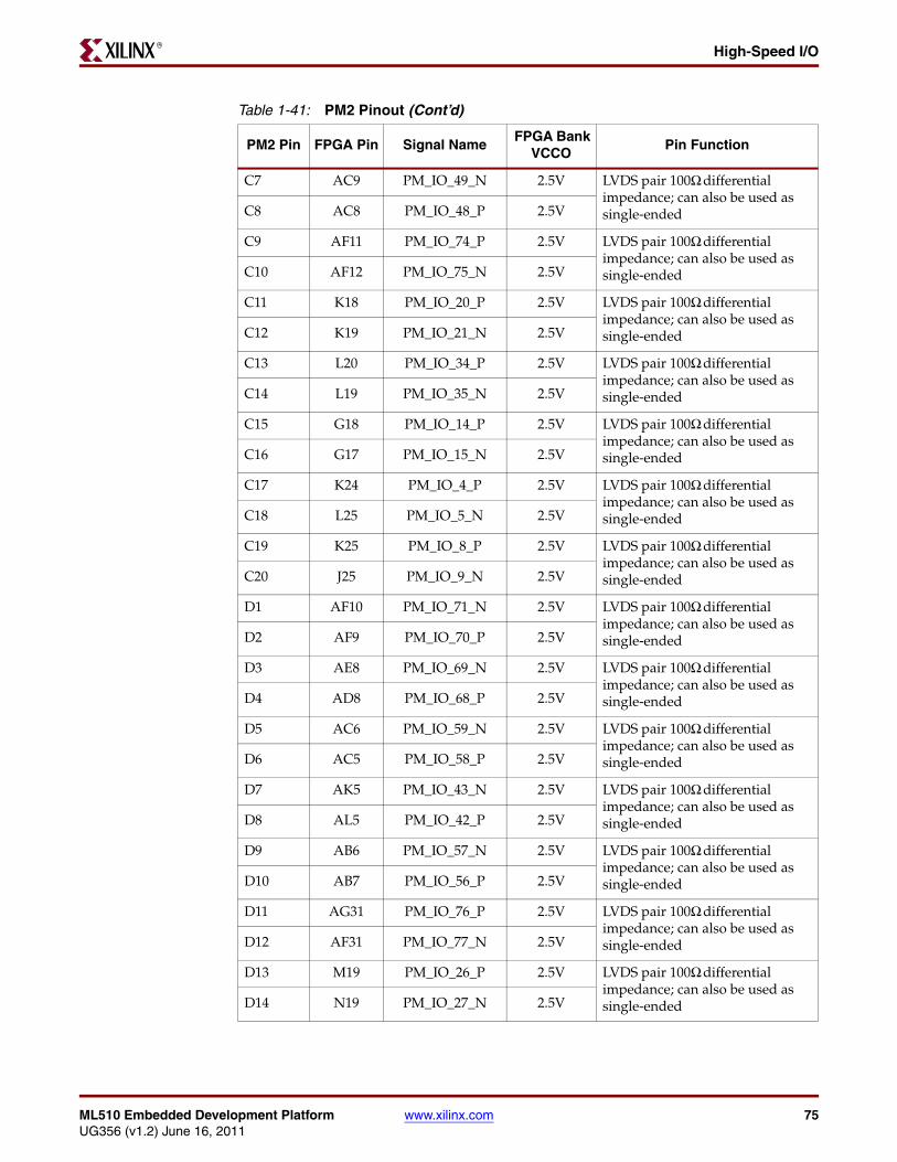
ML510 Embedded Development Platform www.xilinx.com 75UG356 (v1.2) June 16, 2011
High-Speed I/OR
C7 AC9 PM_IO_49_N 2.5V LVDS pair 100Ω differential impedance; can also be used as single-endedC8 AC8 PM_IO_48_P 2.5V
C9 AF11 PM_IO_74_P 2.5V LVDS pair 100Ω differential impedance; can also be used as single-endedC10 AF12 PM_IO_75_N 2.5V
C11 K18 PM_IO_20_P 2.5V LVDS pair 100Ω differential impedance; can also be used as single-endedC12 K19 PM_IO_21_N 2.5V
C13 L20 PM_IO_34_P 2.5V LVDS pair 100Ω differential impedance; can also be used as single-endedC14 L19 PM_IO_35_N 2.5V
C15 G18 PM_IO_14_P 2.5V LVDS pair 100Ω differential impedance; can also be used as single-endedC16 G17 PM_IO_15_N 2.5V
C17 K24 PM_IO_4_P 2.5V LVDS pair 100Ω differential impedance; can also be used as single-endedC18 L25 PM_IO_5_N 2.5V
C19 K25 PM_IO_8_P 2.5V LVDS pair 100Ω differential impedance; can also be used as single-endedC20 J25 PM_IO_9_N 2.5V
D1 AF10 PM_IO_71_N 2.5V LVDS pair 100Ω differential impedance; can also be used as single-endedD2 AF9 PM_IO_70_P 2.5V
D3 AE8 PM_IO_69_N 2.5V LVDS pair 100Ω differential impedance; can also be used as single-endedD4 AD8 PM_IO_68_P 2.5V
D5 AC6 PM_IO_59_N 2.5V LVDS pair 100Ω differential impedance; can also be used as single-endedD6 AC5 PM_IO_58_P 2.5V
D7 AK5 PM_IO_43_N 2.5V LVDS pair 100Ω differential impedance; can also be used as single-endedD8 AL5 PM_IO_42_P 2.5V
D9 AB6 PM_IO_57_N 2.5V LVDS pair 100Ω differential impedance; can also be used as single-endedD10 AB7 PM_IO_56_P 2.5V
D11 AG31 PM_IO_76_P 2.5V LVDS pair 100Ω differential impedance; can also be used as single-endedD12 AF31 PM_IO_77_N 2.5V
D13 M19 PM_IO_26_P 2.5V LVDS pair 100Ω differential impedance; can also be used as single-endedD14 N19 PM_IO_27_N 2.5V
Table 1-41: PM2 Pinout (Cont’d)
PM2 Pin FPGA Pin Signal Name FPGA Bank
VCCOPin Function
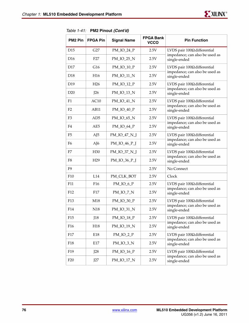
76 www.xilinx.com ML510 Embedded Development PlatformUG356 (v1.2) June 16, 2011
Chapter 1: ML510 Embedded Development PlatformR
D15 G27 PM_IO_24_P 2.5V LVDS pair 100Ω differential impedance; can also be used as single-endedD16 F27 PM_IO_25_N 2.5V
D17 G16 PM_IO_10_P 2.5V LVDS pair 100Ω differential impedance; can also be used as single-endedD18 H16 PM_IO_11_N 2.5V
D19 H26 PM_IO_12_P 2.5V LVDS pair 100Ω differential impedance; can also be used as single-endedD20 J26 PM_IO_13_N 2.5V
F1 AC10 PM_IO_41_N 2.5V LVDS pair 100Ω differential impedance; can also be used as single-endedF2 AB11 PM_IO_40_P 2.5V
F3 AD5 PM_IO_65_N 2.5V LVDS pair 100Ω differential impedance; can also be used as single-endedF4 AE5 PM_IO_64_P 2.5V
F5 AJ5 PM_IO_47_N_J 2.5V LVDS pair 100Ω differential impedance; can also be used as single-endedF6 AJ6 PM_IO_46_P_J 2.5V
F7 H30 PM_IO_37_N_J 2.5V LVDS pair 100Ω differential impedance; can also be used as single-endedF8 H29 PM_IO_36_P_J 2.5V
F9 2.5V No Connect
F10 L14 PM_CLK_BOT 2.5V Clock
F11 F16 PM_IO_6_P 2.5V LVDS pair 100Ω differential impedance; can also be used as single-endedF12 F17 PM_IO_7_N 2.5V
F13 M18 PM_IO_30_P 2.5V LVDS pair 100Ω differential impedance; can also be used as single-endedF14 N18 PM_IO_31_N 2.5V
F15 J18 PM_IO_18_P 2.5V LVDS pair 100Ω differential impedance; can also be used as single-endedF16 H18 PM_IO_19_N 2.5V
F17 E18 PM_IO_2_P 2.5V LVDS pair 100Ω differential impedance; can also be used as single-endedF18 E17 PM_IO_3_N 2.5V
F19 J28 PM_IO_16_P 2.5V LVDS pair 100Ω differential impedance; can also be used as single-endedF20 J27 PM_IO_17_N 2.5V
Table 1-41: PM2 Pinout (Cont’d)
PM2 Pin FPGA Pin Signal Name FPGA Bank
VCCOPin Function

ML510 Embedded Development Platform www.xilinx.com 77UG356 (v1.2) June 16, 2011
Configuration OptionsR
Configuration OptionsThe FPGA on the ML510 Evaluation Platform can be configured by the following major devices:
• Xilinx download cable (JTAG)
• System ACE controller (JTAG)
• Linear Flash memory byte peripheral interface (BPI)
The following section provides an overview of the possible ways the FPGA can be configured.
JTAG (Xilinx Download Cable and System ACE Controller) ConfigurationThe FPGA, two Platform Flash memories, and CPLD can be configured through the JTAG port. The JTAG chain of the board is illustrated in Figure 1-29.
The chain starts at the PC4 connector and goes through the System ACE controller, the FPGA, and the XPM interface. The multiplexers shift the CPU JTAG signals from 2.5V to 3.3V. The resistors provide protection for a 2.5V JTAG probe.
The JTAG chain can be used to program the FPGA and access the FPGA for hardware and software debug.
The PC4 JTAG connection to the JTAG chain allows a host computer to download bitstreams to the FPGA using the iMPACT software tool. PC4 also allows debug tools such as the ChipScope™ Pro Analyzer or a software debugger to access the FPGA.
The System ACE controller can also program the FPGA through the JTAG port. Using an inserted CompactFlash card, configuration information can be stored and played out to the FPGA. The System ACE controller supports up to eight configuration images that can selected using the three configuration address DIP switches. Under FPGA control, the System ACE chip can be instructed to reconfigure to any of the eight configuration images.
The configuration mode should be set to 101 and SYSACE_MODE = 1 (enable), switch SW3 = 00010101 (default setting) to use System ACE configuration. When set correctly, the System ACE controller programs the FPGA upon power-up if a CompactFlash card is present or whenever a CompactFlash card is inserted. Pressing the System ACE reset button also causes the System ACE controller to program the FPGA if a CompactFlash card is present.
X-Ref Target - Figure 1-29
Figure 1-29: JTAG Chain
UG356_c1_28_082508
System ACEController
TSTTDI
TMS, TCK 2
TSTDO
CFGTDO
To/From DebugHeaders J12, P8
CFGTDI
PC
4C
onne
ctor
FPGA
J9
TDI TDO TDI
TDO
U38U37 XPM
InterfacePM2
01
01
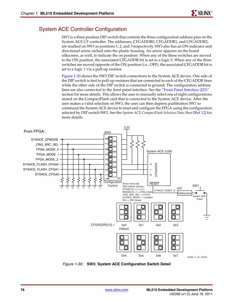
78 www.xilinx.com ML510 Embedded Development PlatformUG356 (v1.2) June 16, 2011
Chapter 1: ML510 Embedded Development PlatformR
System ACE Controller ConfigurationSW3 is a three position DIP switch that controls the three configuration address pins on the System ACE CF controller. The addresses, CFGADDR0, CFGADDR1, and CFGADDR2, are marked on SW3 as positions 1, 2, and 3 respectively. SW3 also has an ON indicator and directional arrow etched onto the plastic housing. An arrow appears on the board silkscreen, as well, to indicate the on position. When any of the three switches are moved to the ON position, the associated CFGADDR bit is set to a logic 0. When any of the three switches are moved opposite of the ON position (i.e., OFF), the associated CFGADDR bit is set to a logic 1 via a pull-up resistor.
Figure 1-30 shows the SW3 DIP switch connections to the System ACE device. One side of the DIP switch is tied to pull-up resistors that are connected to each of the CFGADDR lines while the other side of the DIP switch is connected to ground. The configuration address lines are also connected to the front panel interface. See the “Front Panel Interface (J23)” section for more details. This allows the user to manually select one of eight configurations stored on the CompactFlash card that is connected to the System ACE device. After the user makes a valid selection on SW3, the user can then depress pushbutton SW1 to command the System ACE device to reset and configure the FPGA using the configuration selected by DIP switch SW3. See the System ACE CompactFlash Solution Data Sheet [Ref 12] for more details.
X-Ref Target - Figure 1-30
Figure 1-30: SW3: System ACE Configuration Switch Detail
3.3V
ON
SW3
ConfigurationControl
32
16
78
54
21
0 CF
GA
DD
R
RESET
SYSACE_RESET_N
Shown here with SW3 default settings:CFGA[2:0] 000 (0x0)MODE[2:0] 101 (JTAG mode)JTAG_SRC_SEL = 0 (PC4)SYSACE_MODE = 1 (enable)ON => SW Closed
System ACE (U38)
SW1
Debounce
U31
System ACE Reset
0x0Default
0x1 0x2 0x3
0x4 0x5 0x6 0x7
CFGADDR[2:0] =
UG356_c1_29_100208
From FPGA:
SYSACE_CFMODE
JTAG_SRC_SEL
FPGA_MODE_0
FPGA_MODE_1
FPGA_MODE_2
SYSACE_FLASH_CFGA0
SYSACE_FLASH_CFGA1
SYSACE_CFGA2

ML510 Embedded Development Platform www.xilinx.com 79UG356 (v1.2) June 16, 2011
Configuration OptionsR
Linear Flash Memory ConfigurationData stored in the linear flash can be used to program the FPGA (BPI mode). Up to four configuration images can theoretically be supported.
SW3 BPI default settings:
• CFGA[2:0] 000 (0x0)
• MODE[2:0] 010 (BPI Up mode)
• JTAG_SRC_SEL = 0 (PC4)
• SYSACE_MODE = 0 (disable)
The FPGA RS[1:0] pins can be controlled by SW3 as they are also connected to the SYSACE_CFGA[1:0] (SW3, positions 2 and 3). This allows for manual selection of bit files stored in BPI flash. See the Virtex-5 Configuration User Guide for more information related to configuration via the BPI interface. Refer to the BPI Linear Flash Connectivity diagram in UG191 for more details on the Linear Flash BPI interfaces. [Ref 9]
When set correctly, the FPGA is programmed upon power-up or whenever the Prog button is pressed.

80 www.xilinx.com ML510 Embedded Development PlatformUG356 (v1.2) June 16, 2011
Chapter 1: ML510 Embedded Development PlatformR

ML510 Embedded Development Platform www.xilinx.com 81UG356 (v1.2) June 16, 2011
R
Appendix A
References
This section provides references to documentation supporting Virtex-5 devices, tools, and IP. For additional information, see www.xilinx.com/support/documentation/index.htm.
Documents supporting Virtex-5 FPGAs:
1. DS100, Virtex-5 Family Overview.
2. DS202, Virtex-5 FPGA Data Sheet: DC and Switching Characteristics.
3. UG190, Virtex-5 FPGA User Guide.
4. UG200, Embedded Processor Block in Virtex-5 FPGAs Reference Guide.
5. UG198, Virtex-5 FPGA RocketIO GTX Transceiver User Guide.
6. UG194, Virtex-5 FPGA Embedded Tri-Mode Ethernet MAC User Guide.
7. UG197, Virtex-5 FPGA Integrated Endpoint Block User Guide for PCI Express Designs.
8. UG193, XtremeDSP Design Considerations.
9. UG191, Virtex-5 FPGA Configuration User Guide.
10. UG192, Virtex-5 FPGA System Monitor User Guide.
11. UG195, Virtex-5 FPGA Packaging and Pinout Specification.
12. DS080, System ACE CompactFlash Solution Data Sheet.
Documents supporting Xilinx Platform Studio (XPS):
13. UG111, Embedded System Tools Reference Manual
14. XTP013, EDK Concepts, Tools, and Techniques.
15. UG081, MicroBlaze Processor Reference Guide.
16. OS and Libraries Document Collection.
Documents specific to the ML510 Evaluation Platform:
17. UG355, ML510 Reference Design User Guide.
Documents supporting IBERT:
18. UG213, ChipScope Pro Serial I/O Toolkit.
19. UG029, ChipScope Pro Software and Cores User Guide.
The Xilinx Memory Solutions Web page offers the following material supporting the Memory Interface Generator (MIG) tool:
20. WP260, Memory Interfaces Made Easy with Xilinx FPGAs and the Memory Interface Generator.
21. UG086, Xilinx Memory Interface Generator (MIG) User Guide (for registered users).
22. Demos on Demand, Memory Interface Solutions with Xilinx FPGAs.
23. Xilinx Support - Memory Interface Resources (for registered users).
Documents supporting the LogiCORE Endpoint block for PCIe solutions:

82 www.xilinx.com ML510 Embedded Development PlatformUG356 (v1.2) June 16, 2011
R
24. DS551, LogiCORE Endpoint Block Plus for PCI Express Data Sheet.
25. UG341, LogiCORE Endpoint Block Plus for PCI Express User Guide.
26. UG343, LogiCORE Endpoint Block Plus for PCI Express Getting Started Guide.
Documents supporting the LogiCORE SGMII solution:
27. DS550, LogiCORE Virtex-5 FPGA Embedded Tri-Mode Ethernet MAC Wrapper Data Sheet.
28. UG340, LogiCORE Virtex-5 FPGA Embedded Tri-Mode Ethernet MAC Wrapper Getting Started Guide.
The Xilinx DSP Resources Web page includes documents supporting the System Generator for DSP:
29. System Generator for DSP Getting Started Guide, http://www.xilinx.com/support/sw_manuals/sysgen_gs.pdf
30. System Generator for DSP User Guide, http://www.xilinx.com/support/sw_manuals/sysgen_ug.pdf
31. System Generator for DSP Reference Guide, http://www.xilinx.com/support/sw_manuals/sysgen_ref.pdf
Documents supporting additional embedded processor and LogiCORE IP cores:
32. DS537, XPS_LL_TEMAC (v1.00a) Data Sheet.
♦ XAPP1026, LightWeight IP (lwIP) Application Examples Application Note.
33. DS581, XPS External Peripheral Controller (EPC) (v1.00a) Data Sheet.
♦ XAPP925, Reference System: Using the OPB EPC with the Cypress CY7C67300 USB Controller Application Note.
34. DS531, Processor Local Bus (PLB) v4.6 (v1.00a) Data Sheet.
35. DS402, Device Control Register Bus (DCR) v2.9 (v1.00a) Data Sheet.
36. DS577, XPS 16550 UART (v1.00a) Data Sheet.
37. DS606, XPS IIC Bus Interface (v1.00a) Data Sheet.
38. DS578, PLBV46 to DCR Bridge (v1.00a) Data Sheet.
39. DS444, Block RAM Block Data Sheet.
40. DS445, Local Memory Bus (LMB) v1.0 (v1.00a) Data Sheet.
41. DS641, Microprocessor Debug Module (MDM) (v1.00a) Data Sheet.
42. DS452, LMB Block RAM Interface Controller Data Sheet.
43. DS583, XPS System ACE Interface Controller (v1.00a) Data Sheet.
44. DS573, XPS Timer/Counter (v1.00a) Data Sheet.
45. DS569, XPS General Purpose Input/Output (GPIO) (v1.00a) Data Sheet.
46. DS572, XPS Interrupt Controller (v1.00a) Data Sheet.
♦ XAPP778, Using and Creating Interrupt-Based Systems Application Note.
47. DS481, Util Vector Logic Data Sheet.
48. DS484, Util Bus Split Operation Data Sheet.
49. DS575, XPS Multi-CHannel External Memory Controller (XPS MCH EMC) (v1.00a) Data Sheet.
50. UG081, MicroBlaze Processor Reference Guide: MicroBlaze (v7.00a).
51. DS614, Clock Generator (v1.00a) Data Sheet.
52. DS406, Processor System Reset Module (v2.00a) Data Sheet.
53. DS616, PLBV46 PCI Full Bridge (v1.00a) Data Sheet.
54. DS643, Multi-Port Memory Controller (MPMC) Data Sheet.