the development of a hardware platform for real-time image...
TRANSCRIPT
The University of Western Australia
The Development of a Hardware Platformfor Real-time Image Processing
Final Year Project
Bernard Blackham
Supervisors: A/Prof. Thomas Braunl
A/Prof. Anthony Zaknich
Centre for Intelligent Information Processing Systems
School of Electrical, Electronic and Computer Engineering
Submitted 27th October 2006


1 Stainton PlaceLEEMING WA 6149
27th October 2006
The DeanFaculty of Engineering, Computing and MathematicsThe University of Western Australia35 Stirling HighwayCRAWLEY WA 6009
Dear Sir,
I submit to you this dissertation entitled “The Development of a Hardware Platformfor Real-time Image Processing” in partial fulfilment of the requirement of the awardof Bachelor of Engineering.
Yours faithfully,
Bernard Blackham.

Abstract
In recent years, Field Programmable Gate Arrays (FPGAs) have begun to reach densitiesthat allow large-scale parallel processing to be performed in programmable logic. Theapplication of FPGAs to image processing allows operations to be performed orders ofmagnitude faster than on CPUs or DSPs. The ability to perform a given operation simul-taneously on large sets of data removes the mundane repetitive tasks from CPUs, allowingthem to perform more complicated control tasks.
This project investigates the application of FPGAs to an image-processing platform tar-geted at real-time imaging. A design is developed to optimise the flow of data through theprocessing units (a CPU and a FPGA), such that image data is not required to traverse thesame path multiple times. The design also allows for configurable pre-processing stages tobe performed on the FPGA, freeing the CPU for more complicated control-oriented tasks.One key feature of this platform is the built-in support for two cameras, enabling researchinto hardware-based stereopsis.
Linux is used as the operating system on the device as it offers a solid, familiar platform fordevelopment with a feature-rich toolchain. The developed board is capable of streamingimage data at 60 frames per second from two cameras, through a Spartan-3E FPGAfor pre-processing, and to a 400 MHz PXA255 for analysis. It offers a host of real-world interfaces including motor drivers, position sensors and ADCs, along with USB andEthernet connectivity.
The reliability of the design is analysed by ensuring signal integrity within the circuit. Thehardware’s performance is evaluated and optimised to maximise data throughput from endto end.
v


Acknowledgements
The success of this project would not have been possible without the guidance, assistanceand dedication of a number of people. I would like to give many thanks to my super-visor, Associate Professor Thomas Braunl, for offering the opportunity to develop thisexciting platform, and for his on-going support throughout the project. His knowledgeand experience has helped me to avoid many pitfalls along the way. Thank you alsoto my co-supervisor, Associate Professor Anthony Zaknich, for his advice, feedback andguidance.
A prize needs to be awarded to Ivan Neubronner in the Electronics Workshop, for un-dertaking the most complicated PCB design task the department has seen yet! WithoutIvan’s immense skill and creativity, the project would not have been the success it was. Hewas completely unfazed by the prospect of placing and routing hundreds of componentsin a space the size of a slice of bread, although he may now have a little less hair becauseof it. Thank you for your support, Ivan!
Many thanks to my fellow group members, David English and Lixin Chin, for helpingpull the project together through countless late nights throughout the year. Thank youto Azman and Chang-Su in our lab for not making a fuss as the piles of paper multiplied;to Tom, Grace, Ben, Mark, and rest of the guys in the lab next door who’ve kept meboth sane and amused through all hours of the day and night; to Ali, the super-organisedcomma nazi; Dr. Franz Schlagenhaufer for teaching me each day how else not to designa board; and all my other friends for their encouragement and company. A special thankyou goes to Alysia for her support and affection, and for sharing as much joy in the successof the project as I did.
Finally, I would like to thank my family for tolerating the regular late nights and earlystarts throughout the past year, and for their unconditional love and support. I’m certainthey’re happier than me that it’s all over!
vii


Contents
Letter to the Dean iii
Abstract v
Acknowledgements vii
List of Figures xiii
Abbreviations xv
1 Introduction 1
1.1 Project Scope . . . . . . . . . . . . . . . . . . . . . . . . . . . . . . . 2
1.2 Design Specification . . . . . . . . . . . . . . . . . . . . . . . . . . . . 2
1.2.1 Requirements . . . . . . . . . . . . . . . . . . . . . . . . . . . 2
1.2.2 Constraints . . . . . . . . . . . . . . . . . . . . . . . . . . . . 4
1.3 Major Contributions . . . . . . . . . . . . . . . . . . . . . . . . . . . 5
1.4 Thesis Outline . . . . . . . . . . . . . . . . . . . . . . . . . . . . . . . 6
2 High Performance Embedded Systems 7
2.1 Challenges for High Performance Embedded Systems . . . . . . . . . 8
2.1.1 The Von Neumann Bottleneck . . . . . . . . . . . . . . . . . . 9
2.1.2 Real-time systems . . . . . . . . . . . . . . . . . . . . . . . . . 10
2.2 FPGAs and Image Processing . . . . . . . . . . . . . . . . . . . . . . 11
2.3 Similar Work . . . . . . . . . . . . . . . . . . . . . . . . . . . . . . . 13
2.3.1 EyeBot M1–M5 . . . . . . . . . . . . . . . . . . . . . . . . . . 13
2.3.2 CMUcam . . . . . . . . . . . . . . . . . . . . . . . . . . . . . 14
ix

CONTENTS
2.3.3 Cognachrome . . . . . . . . . . . . . . . . . . . . . . . . . . . 15
2.3.4 MDP Balloon . . . . . . . . . . . . . . . . . . . . . . . . . . . 15
3 Hardware Design 17
3.1 CPU . . . . . . . . . . . . . . . . . . . . . . . . . . . . . . . . . . . . 17
3.2 FPGA . . . . . . . . . . . . . . . . . . . . . . . . . . . . . . . . . . . 19
3.3 Cameras . . . . . . . . . . . . . . . . . . . . . . . . . . . . . . . . . . 21
3.3.1 Camera Configuration . . . . . . . . . . . . . . . . . . . . . . 21
3.3.2 Stereo Vision . . . . . . . . . . . . . . . . . . . . . . . . . . . 22
3.4 SRAM . . . . . . . . . . . . . . . . . . . . . . . . . . . . . . . . . . . 24
3.5 AC97 . . . . . . . . . . . . . . . . . . . . . . . . . . . . . . . . . . . . 24
3.6 JTAG . . . . . . . . . . . . . . . . . . . . . . . . . . . . . . . . . . . 25
3.7 USB Slave . . . . . . . . . . . . . . . . . . . . . . . . . . . . . . . . . 25
3.8 Bluetooth . . . . . . . . . . . . . . . . . . . . . . . . . . . . . . . . . 26
3.9 Infrared . . . . . . . . . . . . . . . . . . . . . . . . . . . . . . . . . . 26
3.10 USB Host . . . . . . . . . . . . . . . . . . . . . . . . . . . . . . . . . 26
3.11 Ethernet . . . . . . . . . . . . . . . . . . . . . . . . . . . . . . . . . . 27
3.12 Servos . . . . . . . . . . . . . . . . . . . . . . . . . . . . . . . . . . . 27
3.13 Motors . . . . . . . . . . . . . . . . . . . . . . . . . . . . . . . . . . . 28
3.14 Encoders . . . . . . . . . . . . . . . . . . . . . . . . . . . . . . . . . . 28
3.15 PSDs . . . . . . . . . . . . . . . . . . . . . . . . . . . . . . . . . . . . 30
3.16 Top board . . . . . . . . . . . . . . . . . . . . . . . . . . . . . . . . . 32
3.17 Power supply . . . . . . . . . . . . . . . . . . . . . . . . . . . . . . . 33
3.17.1 Power control . . . . . . . . . . . . . . . . . . . . . . . . . . . 33
3.17.2 Power switch . . . . . . . . . . . . . . . . . . . . . . . . . . . 34
4 Software Design 35
4.1 Drivers . . . . . . . . . . . . . . . . . . . . . . . . . . . . . . . . . . . 35
4.1.1 Ethernet . . . . . . . . . . . . . . . . . . . . . . . . . . . . . . 35
4.1.2 USB 2.0 Host . . . . . . . . . . . . . . . . . . . . . . . . . . . 36
4.1.3 FPGA . . . . . . . . . . . . . . . . . . . . . . . . . . . . . . . 37
x

CONTENTS
4.1.4 Power Switch . . . . . . . . . . . . . . . . . . . . . . . . . . . 38
4.2 Boot time . . . . . . . . . . . . . . . . . . . . . . . . . . . . . . . . . 38
5 Design Evaluation 41
5.1 Signal Integrity . . . . . . . . . . . . . . . . . . . . . . . . . . . . . . 42
5.1.1 CPU data bus . . . . . . . . . . . . . . . . . . . . . . . . . . . 42
5.1.2 CPU bus control lines . . . . . . . . . . . . . . . . . . . . . . 44
5.1.3 SRAM interface . . . . . . . . . . . . . . . . . . . . . . . . . . 46
5.2 I/O Bandwidth . . . . . . . . . . . . . . . . . . . . . . . . . . . . . . 47
5.3 Power Consumption . . . . . . . . . . . . . . . . . . . . . . . . . . . 51
5.4 Stereo Vision . . . . . . . . . . . . . . . . . . . . . . . . . . . . . . . 52
5.5 Optimising image processing functions on the PXA255 . . . . . . . . 53
6 Conclusion 59
6.1 Future Work . . . . . . . . . . . . . . . . . . . . . . . . . . . . . . . . 59
A Board Detail 63
A.1 Power Control Signals . . . . . . . . . . . . . . . . . . . . . . . . . . 63
A.2 Top view . . . . . . . . . . . . . . . . . . . . . . . . . . . . . . . . . . 64
A.2.1 Jumpers . . . . . . . . . . . . . . . . . . . . . . . . . . . . . . 64
A.2.2 Top board connector pinout . . . . . . . . . . . . . . . . . . . 64
A.3 Bottom view . . . . . . . . . . . . . . . . . . . . . . . . . . . . . . . . 66
A.3.1 Connectors . . . . . . . . . . . . . . . . . . . . . . . . . . . . 67
B Assembly Listings for Section 5.5 71
C libM6 77
References 81
xi


List of Figures
3.1 Block diagram of the EyeBot M6 hardware platform. . . . . . . . . . 16
3.2 Gumstix board with a 400 MHz PXA255 processor, 64 MB of RAM,16 MB of flash and Bluetooth. . . . . . . . . . . . . . . . . . . . . . . 19
3.3 Geometry of the camera positions. . . . . . . . . . . . . . . . . . . . . 23
3.4 Decoding noisy quadrature encoder inputs. . . . . . . . . . . . . . . . 29
3.5 Timing diagram for Sharp’s GP2D02 PSD. . . . . . . . . . . . . . . . 30
3.6 Waveform as generated by the FPGA for clocking the PSDs. . . . . . 31
3.7 Circuitry for the software controlled power supply. . . . . . . . . . . . 34
5.1 The completed board. . . . . . . . . . . . . . . . . . . . . . . . . . . 40
5.2 Mounting of the logic gate to control the data bus buffers’ output. . . 41
5.3 The effect of adjusting output drive strength on the FPGA. . . . . . 43
5.4 Overshoot on the PWE signal. . . . . . . . . . . . . . . . . . . . . . . 44
5.5 The PWE track on the PCB. . . . . . . . . . . . . . . . . . . . . . . 45
5.6 Minimum timing diagram for a VLIO burst-of-four read. . . . . . . . 48
5.7 Empirical performance measurements using VLIO. . . . . . . . . . . . 50
5.8 Images of an alignment test pattern, captured simultaneously fromboth cameras on the EyeBot M6. . . . . . . . . . . . . . . . . . . . . 53
xiii


Abbreviations
ADC Analog to Digital Converter
CIIPS Centre for Intelligent Information Processing Systems
CMOS Complementary Metal Oxide Semiconductor
DMA Direct Memory Access
DSP Digital Signal Processor
EHCI Enhanced Host Controller Interface[1]
FPGA Field Programmable Gate Array
FFT Fast Fourier Transform
GPIO General Purpose Input/Output
I2C Inter-Integrated Circuit
JTAG Standard Test Access Port and Boundary-Scan Architecture1
LUT Look-up Table
MMIO Memory-mapped Input/Output
MMU Memory Management Unit
PCI Peripheral Component Interconnect
PWM Pulse Width Modulation
PSD Position Sensing Device
RTOS Real-time Operating System
SCCB Serial Camera Control Bus[2]
SPST Single Pole Single Throw
USB Universal Serial Bus
VHDL VHSIC (Very High Speed Integrated Circuit) Hardware De-scription Language
VLIO Variable Latency Input/Output
1JTAG is an acronym for Joint Test Action Group, but is the de facto name for the IEEE1149.1 standard entitled Standard Test Access Port and Boundary-Scan Architecture.
xv


Chapter 1
Introduction
Over the past few decades, embedded systems have become increasingly common in
everyday life. Television remotes, alarm clocks, cars and mobile phones contain just a
minute handful of the embedded systems people encounter daily. Embedded systems
are often required to perform tasks within a bounded time frame. For a simple device
such as a remote control, this is not a particularly demanding requirement. However,
for devices that are required to process large volumes of data, much more attention
needs to be given to performance.
Although many problems can be solved by simply harnessing more computational
power, some circumstances do not permit this option due to other constraints, such
as size or power consumption. In cases such as this, smarter, more efficient solu-
tions need to be explored. As embedded systems are generally designed for very
specialised purposes, performance can often be improved by taking advantage of
certain properties of the specific task. For example, a servo motor controlled from
a microprocessor may be handled more accurately by a dedicated timer unit.
Image processing is a computationally intense task which often requires fast, power-
hungry hardware to perform. Real-time image processing incurs further demands
on a system, as the processing of a frame must be completed before the next frame
is ready. Due to the repetitive nature of imaging algorithms, many operations lend
themselves well to parallelisation.
This project investigates methods for customising an embedded system for the pur-
pose of performing real-time image processing. It is anticipated that this system
will be used as a platform for mobile robots with high-performance image process-
1

CHAPTER 1. INTRODUCTION
ing requirements. This requires that size and power consumption be kept minimal
and that the system be sufficiently future-proof to serve the needs of future users.
1.1 Project Scope
The primary goal of this project is to develop a hardware platform primarily tar-
geted at real-time image processing. This platform will serve as the successor to
previous generations of the robotic platform known as the EyeBot. Whilst provid-
ing optimisations for image processing and offering more computational power than
its predecessors, it will also aim to maintain source-level compatibility with existing
software written for the RoBIOS library (used on the previous EyeBots).
A key focus of this platform, referred to as the EyeBot M6, is the ability to accelerate
image processing through the use of a FPGA. It is expected that this will allow the
CPU to dedicate itself to more interesting (but less repetitive) tasks such as the
control system of a robot.
This platform is already being utilised by other students in CIIPS for developing a
range of hardware-accelerated image processing algorithms, from colour-space con-
version to stereo vision[3, 4].
1.2 Design Specification
The design of this system aims to be a general robotics platform, with real-time
imaging capabilities. To fulfil future requirements of a general robotics platform,
commonly used features from existing platforms, such as previous EyeBots, should
be incorporated. For real-time imaging, performance throughout the entire system
should to be maximised in order to satisfy the needs of future users.
1.2.1 Requirements
As the successor to the previous generation of EyeBots, the new hardware platform
should ideally provide the existing functionality in the EyeBot M5. This includes:
• LCD display;
2

1.2. DESIGN SPECIFICATION
• 2 DC motor drivers;
• encoder inputs for each motor;
• 14 servo motor drivers;
• 6 PSD inputs;
• audio input/output;
• analog input channels;
• digital I/O;
• RS-232 interface.
A indication of what constitutes “real-time” is required in order to better specify the
requirements of the system. The OV6630 camera modules intended for use provide
colour images at a rate of 60 frames per second and a resolution of 352×288 (Bayer
pattern). At a bare minimum, the system should be able to operate at this rate to
perform basic operations such as colour histograms.
In addition, to better adapt to real-time image processing applications and serve as
a viable platform for future projects, the following requirements were also added:
• Dual colour cameras — support for two cameras exposes the ability to utilise
stereo vision techniques to obtain depth calculations. The implementation of
stereo vision algorithms on the FPGA is already being investigated by other
students in CIIPS[4].
• High-speed connectivity — the previous generation of EyeBots offered se-
rial and parallel ports for communications. With serial port speeds up to
115200 bps and parallel port speeds up to 921600 bps, it would struggle to
deliver a single colour image frame in under a second. Furthermore, serial and
parallel ports are becoming less common on new PCs, being replaced in favour
of USB and Firewire.
• Wireless capability
• Non-volatile storage
3

CHAPTER 1. INTRODUCTION
1.2.2 Constraints
Time and budgetary constraints limit the range of devices that can be incorporated
into the hardware platform. Thus the underlying goal is to obtain the best possible
performance within the given constraints and at minimal cost. These constraints
are:
Power consumption: As the device will be battery operated, power consumption
should be minimised. Facilities should exist to disable devices which are not
in use.
BGA mounting: Designing boards with BGA (Ball-Grid Array) components re-
quired software that was not available at the start of the project. The venerable
Protel 98 package available to us had no facility for creating or routing BGA
components. In addition, the Electronic Workshop in the department did not
have the necessary equipment to manufacture or populate BGA components.
If fabrication and population of the boards were performed by an external
company, the use of BGA components would double the cost.
PCB size: As the target device is intended for use on mobile platforms such as
robots, the size of the board must be kept to a minimum. As a guide, the
existing EyeBot M5 has dimensions 113 mm×93 mm. A much larger board
would become too impractical for some autonomous devices.
PCB layers: Many PCB manufacturers will manufacture PCBs with up to six
layers. Locating a company willing to do eight or more layers is particularly
difficult, not to mention costly. Thus the design should use no more than six
layers.
RoHS compliance: The RoHS (Restriction on Hazardous Substances) directive
was enforced in the EU (European Union) on July 1st 2006[5], with other coun-
tries around the world expected to follow suit in the following years. Amongst
other things, this directive prohibits the production or import of electronics
goods containing lead within the EU. This has caused a variety of production
issues in the global electronics industry as all manufacturers require retooling
to accommodate lead-free processes.
In 2006, some manufacturers were providing RoHS-compliant alternatives for
their entire product line. However many were still in the conversion process,
4
1.3. MAJOR CONTRIBUTIONS
hampering the availability of RoHS-compliant parts for non-standard compo-
nents.
Additionally, some usability constraints were placed on the design:
• ease of programmability;
• low cost development tools (ideally free);
• debugging interface;
• source-level compatibility with previous EyeBot software.
1.3 Major Contributions
The major contributions of this project are:
• the architectural and schematic design of the EyeBot M6;
• sourcing RoHS-compliant parts for the design;
• the Linux drivers for devices on the board:
– FPGA configuration
– FPGA memory-mapped I/O access
– adapted Ethernet driver
– ported USB 2.0 driver
• the VHDL for communicating with the motors, servos, encoders, and PSDs;
• assistance in writing the VHDL for interfacing to the SRAM controller;
• a library for providing a simple, documented method of accessing the required
hardware;
• performance benchmarking and optimisation of data transfer from the FPGA
to the CPU.
The PCB layout and population of the board was performed by Ivan Neubronner
in the electronics workshop at The University of Western Australia.
5

CHAPTER 1. INTRODUCTION
1.4 Thesis Outline
Chapter 1 offers a brief outline of the project, its motivations and its specification.
Chapter 2 presents some background information in the areas of high performance
embedded systems, hardware-based vision systems and work performed by
other research groups.
Chapter 3 documents the approach taken to the hardware design of the Eye-
Bot M6.
Chapter 4 describes the software drivers and interfaces written for the EyeBot M6.
Chapter 5 evaluates the success of the design and its fulfilment of the design cri-
teria, details the performance obtained from the system and describes how its
performance was enhanced.
Chapter 6 summarises the project and discusses future work on the EyeBot M6
that will follow.
6

Chapter 2
High Performance Embedded Systems
Traditional computer systems operate with a “best effort” approach, where tasks are
attempted using the available resources, but with no guarantees of their successful
completion. Operations may fail to complete on these systems due to unexpected
memory or CPU requirements. For example, dynamic memory allocation leads to
memory fragmentation after repeated allocation and freeing — a tasks that requires a
large contiguous allocation may fail, even if there is sufficient total memory available.
Dynamic allocation can also take a non-deterministic amount of time, making it
impossible to predict the behaviour of the system in all circumstances.
Embedded systems must be designed for reliability. This requires a different per-
spective on design and coding in order to guarantee that the necessary resources
will always be available at runtime. Embedded tasks typically pre-allocate their
total memory requirements at boot, so that the application developer will know im-
mediately if insufficient memory is available. Dynamic allocation is avoided, which
reduces the number of error paths required in the code and the likelihood of memory
leaks being introduced.
Embedded tasks typically also require deterministic execution times in order to
guarantee consistent behaviour of the system under any input condition. System
designers must ensure that sufficient processing power is available for all intended ap-
plications, otherwise risk performance degradation or failure of the system. Systems
utilising real-time operating systems are designed with determinism and reliability
in mind.
High performance embedded systems are subject to the same constraints as regu-
7

CHAPTER 2. HIGH PERFORMANCE EMBEDDED SYSTEMS
lar embedded systems, in that their determinism and reliability is critical. High
performance systems are often required in situations where processing occurs on
large streams of real-time data. These include multimedia applications such as
audio/video streaming and high-bandwidth networking equipment. Requirements
must be met through efficient utilisation of the available hardware.
Fault tolerance is an aspect of reliability that is difficult to anticipate. Process
variation in fabrication can lead to stability issues in memory cells, increased leak-
age currents, and differing behaviours at high frequencies[6]. Operation in high-
temperature environments also reduces the mean time between failure (MTBF) of
a device. The effects of aging need also be considered for devices to operate reliably
in the long-term.
2.1 Challenges for High Performance Embedded Systems
High performance embedded systems are often required to push the limits of their
hardware. Aspects of a computer system which are normally taken for granted must
be analysed much more closely. These include:
• cache performance;
• instruction pipelining;
• interrupt latency;
• impact of interrupts on scheduling;
• the cost of context switching;
• data flow paths within the system.
Depending on the architecture, neglecting to consider some of these factors can
have a huge impact on performance. Yet accurately predicting the performance of
code on a system utilising caches, pipelines and DMA is practically impossible. A
worst-case analysis can be performed, assuming that memory reads never hit the
cache, the instruction pipeline is flushed at every potential opportunity, and that
DMA is continually stealing cycles from the memory bus. This however, is a highly
unrealistic scenario and meaningless in practical systems. Gaining an understanding
8

2.1. CHALLENGES FOR HIGH PERFORMANCE EMBEDDED SYSTEMS
of each component’s effect, their interactions and their impact on overall system
performance, is still beneficial for maximising computational efficiency.
For example, heavily pipelined architectures incur a severe performance penalty on
each unanticipated branch — the Intel XScale processor has a 7 stage pipeline,
with a 4 cycle penalty for branch misprediction. Although modern dynamic branch
predictors typically predict over 90% of branches accurately[7], excessive context
switching can noticeably degrade their performance[8].
Optimising compilers are often aware of the intricacies of the architecture they
target and attempt to maximise the efficiency of the generated assembly. They can
determine an optimal schedule of instructions to minimise register dependencies,
pipeline stalls from memory loads and branch misprediction penalties. However, the
compiler can only work within the constraints of the code it is given. To improve
efficiency, the compiler may require some encouragement to generate more optimal
code. For example, unrolling tight inner loops by hand improves performance on
some architectures, due to fewer branches and the freedom to use more registers.
In addition to the indeterminism of the CPU architecture, the most common em-
bedded languages, C and C++, were not designed to consider timing requirements
of code, and thus compilers are free to generate code as they see fit. No constraints
can be given to specify minimum or maximum execution times. This gives rise to
difficulties when trying to validate timing-critical code[9]. For example, if an oper-
ation involved in video streaming consumes more time than allocated, the following
frame may be dropped. Conversely, if an operation completes in less time than
expected, extra buffers may be required to store the result until it is needed. To
achieve reliability, the number of variables in the system must be reduced. This may
however not always be possible.
2.1.1 The Von Neumann Bottleneck
Computer vision systems have traditionally been implemented on CPU-based ar-
chitectures where a processor alone performs image capture, the desired image pro-
cessing tasks and any post-processing required on the images. Performing these in
real-time on such an architecture requires not only a fast CPU, but also sufficient
memory bandwidth for image capture and processing. This model suffers from the
limitation known as the von Neumann bottleneck[10].
9

CHAPTER 2. HIGH PERFORMANCE EMBEDDED SYSTEMS
The von Neumann bottleneck arises from the separation between the CPU and the
memory, where the data of interest lies. Performing simple tasks on large amounts
of data (such as the pixels of an image), requires each pixel to be read from and
written back to memory. CPU data caches were created to alleviate the pressure on
the memory bus, but their benefits are minimal for continuous streams of data.
Some CPUs (particularly DSPs) offer small amounts of fast internal memory that
can be addressed explicitly, rather than relying on a cache controller. However, very
few offer sufficient internal memory to hold even a single image frame. In addition,
requesting the CPU to copy data from external memory into the internal memory
is a poor use of CPU time. Zinner and Kubinger[11] demonstrate a method of
double buffering image data by co-ordinating DMA requests to pre-populate internal
memory. By using DMA, the CPU can dedicate its time to processing data, whilst
the DMA controller feeds data into internal memory.
Another solution applicable to data acquisition systems such as computer vision
platforms, is to utilise a dedicated hardware device to perform the necessary pre-
processing on the incoming data. This permits the CPU to spend less cycles on
simple repetitive cache-thrashing operations, and more cycles on analysing the re-
sults and making decisions with some degree of intelligence.
2.1.2 Real-time systems
A real-time1 system can be defined as a system that is only considered correct if
its outputs are correct and delivered within a specified deadline[12]. Failure to
meet either criteria constitutes a failure of the system. Real-time systems do not
necessarily need to be high performance, and conversely, high performance systems
do not necessarily need to be real-time. However, the two have certain aspects
common to both. Designing a real-time system requires a holistic approach, that
considers the hardware, the operating system, and all applications, in order to satisfy
the required deadlines.
Real-time systems differentiate between two types of deadlines — hard real-time
deadlines and soft real-time deadlines. Failure to meet a hard real-time deadline may
result in a system failure, whereas failure to meet a soft real-time deadline merely
1“Real-time” in this section refers to the ability of a system to complete tasks in bounded anddeterministic time. This is in contrast to “real-time” image processing, used throughout the restof this thesis, which refers to the rate at which images that can be processed.
10
2.2. FPGAS AND IMAGE PROCESSING
results in degraded system performance. Although the constraints on an image-
processing platform are not necessarily hard deadlines, it must be able to maintain
an average processing rate higher than the required frame rate, and not deplete any
image buffers in the data path. This requires a deterministic and bounded execution
time.
In order to guarantee bounded execution times, careful application (or elimination)
of programming constructs such as unbounded recursion, while loops and interrupts
is required. Intimate knowledge of the hardware architecture is also required to
understand the amount of determinism that can be expected — for example cache
misses, instruction pipeline stalls and failed branch predictions all contribute to
execution time and are exceedingly difficult to predict under all circumstances.
2.2 FPGAs and Image Processing
FPGAs have become increasingly common in applications where DSPs were previ-
ously the only viable solution. This form of large-scale programmable logic provides
specialised signal processing capabilities, which accompanied by the inherent paral-
lelism of hardware, offers an immense performance advantage over a traditional CPU
or DSP model. Additionally, the reconfigurable nature of FPGAs allow updates to
be performed entirely in software, reducing the costs of hardware modifications for
fixing bugs.
One of the most prominent advances in image processing technology is the appli-
cation of FPGAs to real-time image processing. Common image processing tasks
can be performed by a FPGA orders of magnitude faster than by a CPU-based
architecture such as a typical modern Intel processor[13]. Even the latest dedicated
floating-point DSPs, such as Texas Instruments’ TMS320C6200 series of DSPs, take
nearly twice as long as a Xilinx Virtex FPGA to perform a complex object detection
application[14].
One of the most common image processing tasks is edge detection. This is often
used as a precursory step in other algorithms. In most implementations (for ex-
ample, Canny, Sobel, and Robert’s Cross), it can be applied as a simple windowed
convolution function and hence can be parallelised very easily. Venkatesan and
Rao[15] have implemented the Canny edge detection algorithm on a Xilinx Virtex
FPGA running at 16 MHz, and were able to outperform a 1.3 GHz Pentium III by
11
CHAPTER 2. HIGH PERFORMANCE EMBEDDED SYSTEMS
a factor of 20.
More recently, an algorithm called SUSAN[16] has been designed that can perform
both edge and corner detection simultaneously. This has been implemented on a
Xilinx Virtex FPGA in around 1 500 logic cells, and can process 120 images per
second at a resolution of 512× 512 pixels without heavy optimisation[17] — around
6 times faster than a Pentium III running at 450 MHz. Many other researchers
have explored similar routes of implementing vision algorithms on a FPGA, all
achieving respectable results, orders of magnitude faster than with a CPU-based
architecture[18, 19, 20].
FPGAs have clearly proven themselves to be a valuable resource in any image pro-
cessing platform. One design approach would be to simply utilise a pre-fabricated
image processing device and supplement it with a FPGA. This leverages existing
technology and reduces design and production costs. Off-the-shelf hardware exists
that allows an add-on board with a FPGA to be connected into a PCMCIA slot of
a PC, a PCI bus or even directly into a HyperTransport bus alongside the CPUs in
a multiprocessor system. In this way, the FPGA acts as a co-processor to the host
CPU, allowing intensive operations to be offloaded.
Simple tests involving discrete cosine transforms (DCTs) have shown that a Virtex-II
running at 60 MHz could perform DCTs on a 352×288 image at around 590 frames
per second[21]. However, the speed of performing programmed I/O to transfer the
image data to and from the FPGA proved to be major bottleneck. Although the use
of DMA would improve speed, this method highlights the issue of the von Neumann
bottleneck.
An improved architecture would streamline the flow of data through the FPGA,
rather than requiring the CPU to load the image data in and then out of the FPGA.
By connecting the cameras directly to the FPGA, we can instantly take advantage
of the parallelism the FPGA provides. In this model, data flows from the cameras
over dedicated lines to the FPGA, where the images are processed by the FPGA,
and the results are then passed over the CPU’s bus to the CPU for further analysis.
The ability to access multiple memory banks simultaneously from a FPGA would
also give a substantial performance increase to many algorithms[14]. However, as
each memory bank requires in the order of 30 to 50 dedicated pins, this rapidly
consumes much of the FPGA’s I/O capability. The use of sequential-access memory
devices, such as the AverLogic AL422 could reduce this pin count requirement (as
12

2.3. SIMILAR WORK
the addressing pins are no longer required), but some algorithms may require random
access to the image data.
Most of the designs reviewed placed the FPGA on a core system bus, and gave the
FPGA its own memory in addition to the on-chip block RAM. However, none of
the designs involving a camera had it connected directly to the FPGA — this may
have been for configurability and modularity, but the impact on performance was
not noted. With these past experiences in mind, there still exists a large degree of
freedom for the design of the EyeBot.
Although FPGAs are available with sizes in the order of millions of gates, their
freedom and reconfigurability allows larger algorithms to be segmented into several
smaller independent stages, of which only one needs to occupy the FPGA at any one
time. These stages can run sequentially on blocks of data to produce an identical
net result. This technique of run-time reconfiguration has been used to improve the
logic density in a range of applications, including hardware video encoders where
only one third of the logic density is required[22]. Research into OS-level support
for reconfigurable architectures has shown that a more holistic approach to sharing
FPGA resources can create more efficient designs that require much less logic than
an equivalent statically configured design[23, 24].
2.3 Similar Work
2.3.1 EyeBot M1–M5
The previous generations of EyeBots (M1–M5) were created in CIIPS (the Centre for
Intelligent Information Processing Systems) at The University of Western Australia.
They transpired from the need for a viable hardware platform that could enable
research to be carried out in a variety of mobile robotics applications[25]. The
EyeBots offer support for a range of real-world interfaces, including servos, motors,
quadrature encoders, position sensing devices (PSDs) and digital and analog I/O.
Since their creation, they have served as the control platform for soccer-playing
robots, biped walkers, autonomous underwater vehicles and other mobile robotic
devices.
The original EyeBots were built around a Motorola 68332 processor, running at
33 MHz and connected to an 80x60 pixel, 24-bit colour camera. The CPU is ca-
13

CHAPTER 2. HIGH PERFORMANCE EMBEDDED SYSTEMS
pable of performing simple image processing tasks such as Sobel edge detection on
grayscale images at around 10 frames per second and colour object detection at
around 5 frames per second. More detailed analysis of images reduces this frame
rate significantly, such that the results obtained from processing an image are often
outdated and irrelevant by the time the processing is complete.
Despite their slower image-processing capabilities, the core robotics function of the
EyeBot’s design has proven to be quite successful, through its ease of use and versa-
tility. A new design would ideally incorporate all of the existing functionality from
the current EyeBots, and extend it further.
2.3.2 CMUcam
Carnegie Mellon University (CMU) have created a low-cost self-contained image
processing system which can perform basic colour blob tracking at 16.7 frames per
second[26]. The device, CMUcam, utilises an OV6620 CMOS camera, connected to
a Ubicom SX28 microcontroller, running at 75 MHz and offering 136 bytes of SRAM
(less than the size of a single line of camera pixel data!) This simple yet powerful
architecture offers significant size, power and cost advantages over other products
available.
It has been used to successfully guide small autonomous robots, through the RS-232
interface provided. Due to the limited baudrate of the RS-232 interface, it can only
return statistical information about an image in real-time. Entire frame dumps are
possible, but require around 5 seconds per frame. Thus all the desired information
within an image needs to be extracted on the SX28 microcontroller, and condensed
into data that can be transmitted over the RS-232 link in a reasonable amount of
time.
CMU recently released CMUcam2[27], which utilises the faster Ubicom SX52 pro-
cessor and an additional FIFO buffer chip that allows an entire image to be stored
(but only accessed sequentially). This device has even more capabilities than the
original CMUcam, including motion tracking and providing histogram data of colour
channels. The buffer chip in CMUcam2 allows for multi-pass algorithms to be im-
plemented, so long as random access to the image data is not required. Enforcing
sequential access comes with the benefit of design simplicity — addressing an image
frame randomly would require using an additional 17 address pins on the 52-pin
14

2.3. SIMILAR WORK
SX52 processor.
Despite their limitations, both CMUcam and CMUcam2 demonstrate what can be
achieved with restricted processing power and a tiny amount of RAM.
2.3.3 Cognachrome
The Cognachrome is a commercial vision system based around a Motorola 68332
processor, but utilises specialised hardware that allows 25 objects to be tracked at
up to 60 frames per second[28]. The system’s software can be configured to track
up to three different colours at once, and relay information about the positions of
the detected objects over a serial connection.
These devices were used on the soccer robots that won the first International Micro
Robot World Cup Soccer Tournament in 1996. They have also been used in robots
developed at MIT, designed to catch flying objects. Their high frame rate offers very
rapid snapshots of their surroundings, allowing for fast reactions. Unfortunately,
very little information about their hardware acceleration is available.
2.3.4 MDP Balloon
Cambridge University are currently working on a board known as the MDP (Multi-
disciplinary Design Project) Balloon board[29]. This board uses Linux and provides
a host of interfaces for extensibility. Whilst this is not specifically targeted at image
processing, version 3 of the board includes an Intel PXA270 processor running at
520 MHz and a 400 000 gate FPGA.
The PXA270 features Intel “Quick Capture”, allowing a camera to be connected
directly to the CPU without any extra circuitry. Colour space conversion can be
performed by on-chip hardware, which supports a range of common image formats
provided by CMOS cameras. Combined with the on-board FPGA, this would serve
as a suitable platform for image processing. However, as images are streamed into
RAM, image processing algorithms are still subject to the von Neumann bottleneck.
15

Figure 3.1: Block diagram of the EyeBot M6 hardware platform.

Chapter 3
Hardware Design
Several months of work were dedicated solely to the design of the hardware platform.
The process of selecting parts and ensuring the correctness of the final schematic
proved to be quite time consuming. The design and schematic went through several
iterations before being transferred to a PCB layout. A block diagram of the final
design is shown in Figure 3.1.
Most devices are connected to either the CPU (Gumstix) or the FPGA. The design
frees the CPU from both repetitive and timing-critical tasks, by delegating those
to the FPGA. Similarly, the FPGA is not directly involved with any hardware that
requires a large amount of logic to control. The resource in highest demand is the
central bus on which the CPU, FPGA, USB and Ethernet chips reside.
The following sections detail the components of the design and the rationale behind
the design decisions.
3.1 CPU
The constraint on avoiding BGA components drastically reduced the number of
options available — the range of CPUs available in standard lead packages did not
extend past 200 MHz. The fastest CPUs that could be obtained in a non-BGA
package were Samsung’s S3C44B0 at 66 MHz, the Philips LPC2100 at 70 MHz, and
more impressively, Atmel’s AT91RM9200 at 180 MHz and CirrusLogic’s EP9302 at
200 MHz.
17

CHAPTER 3. HARDWARE DESIGN
However, none of the available devices were deemed to have sufficient computational
power or I/O for the future needs of an EyeBot. Thus the focus moved to searching
for readily available single board computers (SBCs). This proved to be a much more
promising approach — many companies provide SBC devices with a range of faster
CPU speeds. Regardless of which board was chosen, the final design would thus
require two boards — the SBC and a second board incorporating the FPGA and
other I/O interfaces.
Compulab, an Israeli company, manufacture compact, powerful SBCs based around
a variety of architectures (from PXA255s and PXA275s through to Pentium-IIIs)
all on compact boards around 70 mm× 60 mm in size. They also appeared to be an
attractive price, until it was discovered that they required an expensive evaluation kit
to be purchased first. However, with a wide variety of processors, it did demonstrate
what was possible. In particular, they highlighted that for low power consumption,
the PXA255 and PXA270 processors were good performers.
Another device in a similar league is the Sun SPOT — based around an ARM920T
core at 180 MHz, with a strong resemblance to the AT91RM9200 and are designed for
real-world sensing and low power consumption. A German company, F&S Electronik
Systeme, manufacture a family of devices called PicoMOD. These utilise a 400 MHz
Samsung ARM-9 part in a compact form factor, with 32 MB of RAM.
Gumstix Inc. offer a 400 MHz ARM-9 PXA255 processor with 64 MB of RAM, in
a tiny 20 mm × 80 mm package, as shown in Figure 3.2. This was chosen as the
most cost-effective solution. It provides much more computational power than the
alternatives in the same price range and also comes with Linux pre-installed. A build
environment is freely downloadable, allowing the image to be modified as desired
and with minimal hassle involved in rebuilding the entire system. Additionally,
drivers are written and functional for many peripherals including Ethernet, audio,
USB slave, and the LCD.
The Intel PXA255 processor (featured on the Gumstix and other SBCs examined)
offers the ARMv5TE instruction set. The “E” denotes the DSP extensions to the
ARM instruction set[30]. This includes support for single-cycle instructions such as:
saturating addition/subtraction — when processing image data, saturating re-
sults is more desirable than overflowing. Avoiding an explicit check for overflow
reduces the number of instructions required and minimises costly branches.
18

3.2. FPGA
Figure 3.2: Gumstix board with a 400 MHz PXA255 processor, 64 MB of RAM, 16 MBof flash and Bluetooth.
These are typically found in inner loops of code, where the maximum benefit
can be attained.
16x16-bit and 16x32-bit multiply/accumulate — this is another common task
seen when applying image masks, performing alpha blending, averaging pixel
values or calculating dot products. The ability to perform each multiply/accumulate
in a single instruction cycle presents enormous potential for optimising image-
processing algorithms.
count leading zeroes — this operation is primarily used for normalisation. Whilst
not as applicable to processing pixel data directly, it can be used to optimise
the speed of division operations.
3.2 FPGA
By utilising a FPGA for image processing, many of the concerns about reliability
and determinism of image processing tasks are eliminated. Dedicated hardware is
not subject to variations from interrupts, pipeline stalls, DMA accesses, and other
external factors. This creates a more predictable system and frees up the CPU for
control-oriented tasks.
19
CHAPTER 3. HARDWARE DESIGN
Part LUTs I/O pins Block RAM MultipliersAltera Cyclone EP2C20 18,752 142 234 Kbits 26Lattice ECP2-12 12,000 131 221 Kbits 24Xilinx Spartan-3E XC3S500E 9,312 158 360 Kbits 20
Table 3.1: Comparison of largest available FPGAs in non-BGA packaging from variousmanufacturers.
FPGAs from several vendors were investigated including Altera, Lattice Semicon-
ductor and Xilinx. All vendors provide development environments for their FPGAs
free of charge. Due to the BGA constraint, the analysis focused on the largest
FPGAs available in non-BGA packaging from various manufacturers, as shown in
Table 3.1. The logic unit counts between vendors are not directly comparable, and
only give a general guide to the size of a FPGA[31, 32, 33]. Due to structural dif-
ferences in the internal design of FPGAs, certain designs may favour one device or
another.
The Xilinx Spartan-3E was chosen for a number of reasons:
• more block RAM — for processing image data, the ability to store and access
more image data in fast block RAMs will increase the performance of algo-
rithms. Although the Altera’s block RAMs provide finer-grained access, it did
not justify 35% less block RAM.
• a higher user I/O pin count — after connecting 2 cameras, the CPU bus, the
SRAM, 14 servos, 4 motors, 6 PSDs and 8 digital I/O lines, at least 134 pins
are required.
• lower cost — at the time of investigation, the Altera EP2C20 was double the
price of the Xilinx XC3S500E.
• experience — Xilinx parts and tools are already used within the department
for other vision-related projects.
This choice came at the expense of extra logic that would have been gained by
choosing the Altera EP2C20.
The FPGA is connected to the CPU such that it can be configured simply by writing
the configuration stream into the address space of the FPGA. Partial reconfiguration
20

3.3. CAMERAS
is also supported by exposing the SelectMAP interface of the FPGA. This allows
the system to utilise dynamic runtime partial reconfiguration, but at the expense
of half the bus bandwidth, as 8 bits of the 16-bit data bus are dedicated to the
configuration interface.
3.3 Cameras
The EyeBot M6 allows two cameras to be connected directly to the board. The
motivation for this is to allow experimentation with stereo vision algorithms on the
FPGA.
The board is designed for the OmniVision OV6630 camera, mounted on a C3038
module manufactured by CoMedia. This camera provides 352×288 colour images
(Bayer format) at up to 60 frames per second and provide a configuration interface
that allows control over gain, white balance, hue and gamma settings.
A similar model is available (the AA763) with a compatible pinout, and provides
VGA resolution images (640×480), should the extra resolution be required. Al-
though the FPGA may require some modifications to capture the larger image, no
hardware changes are necessary.
3.3.1 Camera Configuration
The OV6630 cameras are configured via a protocol known as SCCB[2] — a two-
wire interface with a protocol specification that maps quite cleanly onto the I2C[34]
protocol developed by Philips. Previous FPGA-based circuits utilising this camera
communicated with the camera directly from the FPGA. Implementing the SCCB
protocol in VHDL consumed a large amount of the FPGA’s logic. As the PXA255
has an I2C bus master on-chip, it was decided to utilise it in order save the logic
space in the FPGA.
The SCCB interface on the OV6630 camera has a hard-coded slave address. If both
cameras are placed on the same SCCB bus, confusion would arise when attempt-
ing to configure the registers. This may not be an issue if only writes were ever
performed by the master (the PXA255), as it would equate to both cameras being
programmed identically, and some brief bus contention when the cameras acknowl-
edge the transmission.
21

CHAPTER 3. HARDWARE DESIGN
A better solution, utilises the observation that when a camera is placed into standby
mode (by holding a high level on its PWRDN pin), it will not respond to SCCB
commands. It will however retain its current configuration. Thus two (or more)
cameras can be configured from the same SCCB bus by powering down all the other
cameras that are not being configured. This method is used to configure the two
cameras on the board.
3.3.2 Stereo Vision
The camera connectors are positioned parallel on the board at fixed positions. This
places the baseline width of the cameras at 66 mm, closely approximating the dis-
tance between the eyes of an adult human. However, unlike the human eyes, the
cameras do not have the ability to turn towards each other. This imposes a mini-
mum distance that any stereo vision algorithm can function at, as the object may
be out of view of one or both cameras. This is demonstrated in Figure 3.3 — the
unshaded area at the top is the region in which objects appear in both frames. Light
grey areas represent regions where objects only appear in one camera’s field of view.
The dark grey regions are out of view of both cameras.
Despite the limitations created by immovable cameras, a fixed geometry eases the
burden on a stereo vision system by eliminating many unknown factors. Addition-
ally, by fixing the positions of the cameras appropriately on the board, it should be
possible to guarantee that:
• the CCDs of both cameras always lie in the same plane;
• the scan lines of both cameras are parallel;
• the images are aligned vertically.
If these three conditions are satisfied, corresponding scan lines of the cameras repre-
sent the epipolar lines required to utilise the epipolar constraint in stereo vision[35].
This eliminates the need for the rectification pre-processing stage that is typically
required to satisfy the epipolar constraint. That is, for any given point in an image,
the corresponding point from the opposite image lies on the same epipolar line, and
thus the same scan line. To allow for slight deviations, algorithms such as SAD
(Sum of Absolute Differences) will limit their search space to a small number of
scan lines above and below the theoretical epipolar line.
22

3.3. CAMERAS
Figure 3.3: Geometry of the camera positions, as fixed by the design of the board. Darkgrey regions represent blind spots for both cameras. Light grey regions areonly visible by one of the two cameras.
23

CHAPTER 3. HARDWARE DESIGN
This model is based on the premise that both CCD cameras are manufactured
identically — it was later discovered that this is often not the case (see Section 5.4).
3.4 SRAM
Although the Xilinx Spartan-3E contains a total of 45 kB of block RAM, an entire
352× 288 image consumes 99 kB. Thus a secondary storage medium is required in
order to perform any multi-pass image processing operations. A static RAM device
was chosen in preference to dynamic RAM. The reasons for this are:
• no DRAM refresh logic is required, reducing the complexity of the FPGA and
preserving logic for image-processing functions;
• the large storage densities offered by DRAM are not required — even a 1 MB
SRAM can store 10 camera frames;
• it allows for algorithm designers to split complicated algorithms — i.e. if an
algorithm is too large to fit in a single FPGA image, the designer can opt
to partition the algorithm into two (or more) phases performed by different
FPGA images, utilising the SRAM as temporary storage space for intermediate
results. As reconfiguring the FPGA takes in the order of 100 ms, any DRAM
that relied on the FPGA for refreshing would have lost its contents.
The Cypress CY7C1383D is a 2 MB (1024 × 18-bits) SRAM that can be accessed
synchronously at up to 100 MHz. There also exists a 1 MB version (the Cypress
CY7C1363D), that is pin for pin compatible with the CY7C1383D.
As the current drawn by the SRAM even in standby mode is quite substantial
(70 mA), a facility is provided on the board to disconnect power from the SRAM
when not required.
3.5 AC97
The Philips UCB1400 provides a standard AC97 interface to the PXA255 and offers
three audio inputs, two audio outputs, four analog inputs, 10 digital input/outputs,
and a touchscreen controller. Software support already exists for this device on the
24

3.6. JTAG
Gumstix platform. Its tiny footprint (8 mm × 8 mm) aided to minimise the overall
size of the board.
3.6 JTAG
JTAG is a standard interface and protocol used for externally examining PCBs and
ICs. The JTAG interface of the PXA255 is exposed primarily for reflashing the
bootloader when recovering from a damaged flash image. This is generally the only
circumstance where JTAG is necessary. If the bootloader is intact, the kernel and
filesystem can be reflashed over serial or Ethernet. JTAG could potentially be used
for debugging purposes, however most code that will be written for the board will
be userspace Linux code which can be debugged much more easily using gdb.
On initial revisions of the Gumstix board, the JTAG connections were exposed
through the top connector. Unfortunately, this was altered on newer revisions —
the JTAG pins must now be accessed via test points on the board. These test
points are not accessible when the Gumstix is mounted on the EyeBot M6, so in-
place recovery is not possible.
3.7 USB Slave
The PXA255 offers a dedicated USB 1.1 slave port to allow the platform to act as a
USB device. This mode of operation is well supported by Linux, and is accompanied
by drivers that enable the PXA255 to act as a mass storage device, an Ethernet
adapter or an RS-232 serial port. Further drivers could also be written to support
any form of device. One potentially useful driver would allow the board to emulate
a webcam, streaming video data from the EyeBot’s cameras.
The mass-storage device driver can be used for loading user programs onto the Eye-
Bot. As USB is becoming more common-place than RS-232 on modern computers,
this presents an ideal successor to the current serial method used for loading pro-
grams. Additionally, the USB interface can operate at 12 Mbps — over 100 times
faster than the RS-232 interface.
A USB device is able to draw up to 500 mA off the 5 V rail[36]. The EyeBot takes
advantage of this by drawing power from the USB rail if it is not otherwise powered,
25

CHAPTER 3. HARDWARE DESIGN
allowing use of the device without a battery. This is achieved by positioning a
Schottky barrier diode from the USB rail to the 5 V rail of the EyeBot M6, to
ensure that power does not flow back into the USB host. The Schottky barrier
diode is chosen for its low forward voltage drop.
The software needs to ensure that large current consumers such as the servos and
motors are not turned on whilst powered from the USB port. This can be determined
by either observing the status of the PWRON line at power-up, or reading the
battery voltage through the ADC channel.
3.8 Bluetooth
The Gumstix board provides an integrated Bluetooth module capable of speeds up
to 921 600 bps. This will allow EyeBots to communicate wirelessly either with each
other, or a central “base station”. It also allows the possibility to interact with the
EyeBot from a PDA or mobile phone with Bluetooth capabilities.
3.9 Infrared
An infrared sensor (TSOP1738) is connected to a GPIO line on the PXA255. This
device is the same as that used on the previous generations of EyeBots and is capable
of decoding standard 38.4 kHz signals. A powerful software package called LIRC
supports decoding infrared signals from a variety of receivers. A small amount of
extra software will be required in order to convert the signal from the TSOP1738
to a list of time intervals between pulses. The LIRC software package is capable of
performing the decoding and can be programmed for a variety of remote controls.
3.10 USB Host
USB 2.0 connectivity was decided to be an essential component of the hardware
platform, as it allows a large and diverse range of devices to be connected, supple-
menting the existing on-board devices. Such devices could include extra webcams,
serial adapters, mass storage devices, mobile phones, GPS units or wireless adapters.
26

3.11. ETHERNET
At the time of writing, most of the USB 2.0 controller ICs on the market interfaced
directly to a PCI or PCI-X bus. Very few non-PCI devices were available. The most
promising candidate was the Philips (now NXP) ISP1761. Existing application
notes[37] describe the required connections for the PXA255, implying that it had
been used with success in the past. Existing Linux drivers for the device also reduced
development time, but required porting to recent versions of the Linux kernel.
3.11 Ethernet
Gumstix produce Ethernet add-on modules for their boards that utilise the SMC
LAN91C111 Ethernet chip. Unfortunately, sourcing these ICs was not a trivial
task, so the search began for a different IC. Desirable features in a chip included
existing drivers for both the Linux kernel and the U-boot bootloader, no specific bus
requirements (e.g. PCI-only chips) and the ability to support 100 Mbit Ethernet.
The chosen device was the ASIX AX88796B. As this device is compatible with the
venerable NE2000, drivers exist for almost every operating system and platform! It
is capable of both 10 Mbps and 100 Mbps connections, can be connected directly to
the PXA255’s data bus and requires a minimum of extra circuitry.
The physical interface requires an isolating transformer to protect the EyeBot from
unexpected voltages should the Ethernet be plugged into a malfunctioning device,
phone line or other dangerous voltage source. It also serves to provide the correct
impedance of 100 Ω for the Ethernet connection, ensuring that maximum power is
transferred across the Ethernet line, and maintains the signal integrity by ensuring
that transmission line effects such as reflections do not occur.
3.12 Servos
The board supports 14 dedicated servo motors — the same number as supported
by the current EyeBot M5. Each servo is connected to an output pin on the FPGA
and driven by logic in the FPGA. As the signalling for positioning servos is timing
critical, dedicated logic on the FPGA ensures that the servos do not fail, regardless
of the state of the CPU.
27

CHAPTER 3. HARDWARE DESIGN
3.13 Motors
The board supports four independently controlled motors, driven via two L293DD
push-pull driver ICs connected in a H-bridge configuration. Like the servos, the mo-
tor control lines are connected to the FPGA. Each of the four motors are controlled
by a direction line and an enable line. Inverting the direction line will invert the
polarity of the connections to the H-bridge, reversing the motor’s direction. Each
motor’s speed is adjusted by a PWM controller inside the FPGA, connected to
the enable line for the H-bridge. The PWM controllers driving these four motors
are configured to be 90 out of phase with each other, in order to smooth out the
instantaneous current requirements of the motors.
The power source for the motors is selectable via a jumper block that allows con-
nection directly to the battery rail or the 5 V rail. Alternately, any arbitrary source
may be connected to the motors by feeding it to the centre pin of the jumpers1.
The 6-pin motor connector is identical to that used on the current EyeBot M5s,
with the pinout given in Appendix A.
3.14 Encoders
Each motor can have an associated quadrature encoder that provides feedback on
the current shaft position. Decoding these encoders is yet another task which is
better suited to the FPGA, saving the CPU from continuous streams of interrupts.
It also guarantees that no shaft rotations will be missed, for example should the
CPU become heavily loaded.
Encoder signals are typically subject to mechanical jitter as the switch contacts open
and close, giving rise to an electrical signal with multiple and ill-defined rising and
falling edges. Many designs do not allow for this jitter, leading to unreliable results;
yet reliably decoding noisy encoders is well-documented. Numerous approaches can
be taken[38, 39], but they all observe that only a handful of the possible transitions
are actually valid occurrences and the others can be safely ignored.
The technique used on the EyeBot M6 (shown in Listing 3.1) is based upon the
observation that a definitive event occurs only when both encoder inputs become
1Users must ensure the motors operate within the specifications of the L293DD driver IC (i.e.motor voltage is between 5 V and 36 V and the current per motor does not exceed 600 mA).
28

3.14. ENCODERS
if (rising_edge(CLK)) then
enc <= ENC_A & ENC_B;
case enc is
when "00" => eevent <= ’0’;
when "11" => eevent <= ’1’;
when "01" => edir <= ’0’;
when "10" => edir <= ’1’;
end case;
last_eevent <= eevent;
if (last_eevent = ’0’ and eevent = ’1’) then
if (edir = ’0’) then
encval <= encval - 1;
else
encval <= encval + 1;
end if;
end if;
end if;
Listing 3.1: VHDL code used for decoding quadrature encoder inputs.
ENC_A ENC_A
ENC_B
ENC_A
ENC_B
eevent
ENC_A
ENC_B
eevent
edir
Figure 3.4: Decoding noisy quadrature encoder inputs.
29
CHAPTER 3. HARDWARE DESIGN
> 70 ms< 0.2 ms
> 1 ms > 1.5 ms
D7 D6 D5 D4 D3 D2 D1 D0
Input
> 70 ms< 0.2 ms
> 1 ms > 1.5 ms
D7 D6 D5 D4 D3 D2 D1 D0
Input
Output
> 70 ms< 0.2 ms
> 1 ms > 1.5 ms
D7 D6 D5 D4 D3 D2 D1 D0
Input
Output Output
Figure 3.5: Timing diagram for reading an 8-bit distance value from Sharp’s GP2D02PSD (not drawn to scale).
high. This event is latched until both encoder inputs have returned low. The
direction of the event is determined by the most recent input to have transitioned
from a low to a high. By sampling the encoder inputs every 20 ns (from the 50 MHz
clock), the probability of missing an event is practically zero. The resulting signals
are shown in Figure 3.4.
3.15 PSDs
The position sensing devices (PSDs) are connected to the FPGA’s input pins. The
decoding of the six PSDs can be performed by the FPGA in parallel, freeing the
CPU from this repetitive task. The CPU can simply read a memory location to
retrieve the latest reading from the PSDs. What was previously 650 lines of m68k
assembly code for the EyeBot M5, is replaced by a total of 120 lines of VHDL.
As per the datasheet for the Sharp GP2D02 device, a very specific waveform is
required to be clocked into the device (shown in Figure 3.5). The VHDL code to
do this can actually be made exceedingly small — Listing 3.2 shows the 7 lines of
code written to perform this. The operation of this VHDL code is not immediately
obvious, so an explanation follows.
The waveform requires 8 brief pulses followed by a longer pulse, with the timing
constraints given on the diagram. The FPGA is clocked by a 50 MHz crystal oscil-
lator, giving a base clock signal with period 20 ns. To minimise the logic required to
create this waveform, the approach taken is to clock this signal into a binary counter,
30

3.15. PSDS
Figure 3.6: Waveform as generated by the FPGA for clocking the PSDs.
PSD_CLK_Out <= ’0’;
if (CLK_Divisor_Reg(21 downto 18) = "0000") then
PSD_CLK_Out <= not(CLK_Divisor_Reg(13));
if (CLK_Divisor_Reg(17) = ’1’) then
PSD_CLK_Out <= ’1’;
end if;
end if;
Listing 3.2: VHDL code for generating the PSD clock input signal.
31

CHAPTER 3. HARDWARE DESIGN
and connect the appropriate logic to the output bits of the counter to generate the
waveform.
Given the constraint of a minimum of 70 ms between successive PSD reads, a 22-bit
up-counter is used, giving a period between reads of 20 ns × 222 = 83.9 ms. The 8
brief pulses are generated by connecting the output to the inverse of the 13th bit,
when bit 21 through to bit 17 are all zero. This essentially means that the 3 bits
from 16 to 14 are counting through the 8 required pulses. The bits retrieved from
each PSD’s output are fed into a shift-register. The on-time of the waveform is thus
given by 10 ns× 213 = 0.164 ms, within the bounds required by the PSD.
To obtain the final high pulse, the output of the waveform generator is sent high if
bits 21 through to 18 are zero, but 17 is a one. The resulting waveform is displayed
in Figure 3.6.
3.16 Top board
A secondary daughterboard is needed for several reasons:
• The Gumstix has connectors on both sides of the board, each presenting a
different set of signals. The bottom connector mates with the base board of
the EyeBot M6, whilst the top connector requires a connection to bring the
necessary lines back to the base board. The signals to connect to the LCD are
located on the top connector. By placing the LCD on this board, the number
of pins that need to be routed back down to the lower board is minimised.
• LCD modules come in varying sizes, colour depths and costs. As the PXA255’s
LCD controller is configurable for many types of LCDs, restricting the Eye-
Bot M6 to one specific LCD is not desirable. By placing the LCD on a daugh-
terboard, LCDs can be interchanged, depending on the application.
• Additional general purpose I/O (GPIO) lines — all 20 LCD lines can also act
as general purpose I/O. If an application requires more digital I/O and can
function without a 16-bit colour LCD, these lines can be utilised.
• A lot of difficultly was experienced in attempting to source a RoHS compli-
ant speaker in Australia. By moving the speaker to a daughterboard, more
32

3.17. POWER SUPPLY
flexibility is given to the overall design. The audio amplifier circuitry was
also placed on the top board with the speaker, reducing the complexity of the
routing on the base board.
In order to ensure that different top boards are interchangeable, a standard interface
was created. A rudimentary auto-detection method identifies which type of board
is connected by defining certain LCD lines to be pulled up or pulled down. On
start-up, the bootloader will read the ID of the connected device and pass this ID
to the Linux kernel. The kernel can use this to correctly configure the LCD, and
other devices connected to the top board.
3.17 Power supply
Given the array of devices on-board, numerous voltages are required. The FPGA
requires 1.2 V, 2.5 V and 3.3V, the USB host requires 5 V, and the LCD requires
3.0 V, 3.6 V and 8.0 V. The main 5 V rail is supplied by an LM2678 switch-mode
power supply, capable of passing 5 A of current. A TPS75003 regulator provides
the three voltages required by the FPGA, whilst the LCD power supply is regulated
with simple zener diodes.
Fast-response polyswitches are used on the board in preference to fuses, to avoid
the hassles associated with fuses and the temptation of replacing them with an
overspecified value. The servos and USB host ports have an independent polyswitch
which can be monitored by the FPGA to detect in software if the polyswitch has
tripped.
3.17.1 Power control
In order to fulfil the goal of minimising power consumption, many devices on the
board were given facilities to be disabled or placed into a low power mode. A number
of control signals were dedicated to disabling power for certain devices. These signals
are documented in Appendix A. Devices that do not have a direct control signal
for disconnecting power can be powered down through software. Specifically, the
Ethernet and USB devices can be placed into standby mode using configuration
registers and hence do not require a dedicated control line.
33

CHAPTER 3. HARDWARE DESIGN
1
1
2
2
3
3
4
4
D D
C C
B B
A A
Title
Number RevisionSize
A
Date: 10/16/2006 Sheet ofFile: C:\FYP-DLB\Eyebot M6\PowerSupply.SchDocDrawn By:
22uH
L2
OUT 1
IN2 CBOOST 3
GND4
FB 6ON/OFF7U14
LM2678
22uC128
22uC129
22uC130
D26TQ045S
220uC132
220uC131
PWRON
S1AON / OFF
33KR65
15KR72
10KR66
PWRSW
100K
R73
10nC135
BZB984 3V9
D1
12
J23
8 - 15VDC D36TQ045S
F4
3A
VBATT
FB7
10uC178
VBATT
5VR
P0C12801
P0C12802 P0C12901
P0C12902 P0C13001
P0C13002
P0C13101
P0C13102 P0C13201
P0C13202
P0C13501
P0C13502
P0C17801
P0C17802
P0D101
P0D102
P0D103
P0D202
P0D203
P0D302
P0D303
P0F401 P0F402
P0FB701 P0FB702
P0J2301
P0J2302
P0L201 P0L202
P0R6501
P0R6502
P0R6601
P0R6602
P0R7201
P0R7202
P0R7301 P0R7302 P0S1A01 P0S1A02
P0U1401
P0U1402
P0U1403
P0U1404
P0U1406 P0U1407
Figure 3.7: Circuitry for the software controlled power supply.
3.17.2 Power switch
In order to avoid the reliability issues associated with mechanical on/off switches,
the design utilises a single SPST pushbutton. This, along with a GPIO pin from the
PXA255 (connected to PWRON in Figure 3.7), is connected to the on/off pin of the
main power supply IC (LM2678) through a resistor network. Both the switch and
the GPIO send the on/off pin high, supplying power to the rest of the device. Thus
in order for the device to stay on, the GPIO pin must be set high before the switch
is released. The software on the PXA255 can then turn the device off by releasing
the GPIO line.
By connecting an input pin on the PXA255 to PWRSW, the PXA255 can also sense
when the button has been depressed or released. The zener diodes protect the CPU
from excessive voltages, as VBATT may potentially be as high as 40 V.
34

Chapter 4
Software Design
4.1 Drivers
Linux is a freely available operating system and has already been ported to the
PXA255 processor and Gumstix platform. This allowed development to occur much
more rapidly, as most of the hardware was already supported. However, some of the
devices added onto the EyeBot M6 are not in canonical locations and hence certain
drivers needed to be modified in order to detect them.
4.1.1 Ethernet
The ASIX AX88976B Ethernet chip is advertised as NE2000-compatible — i.e. it is
designed so that a driver for a standard NE2000 network controller will also operate
correctly with this chip. This was nearly the case but some modifications were made:
• As the address lines were connected starting from A1, rather than the canonical
A0, all register offsets were shifted left one bit.
• DMA support for the PXA255 processor was added to increase throughput.
• Support for link status information through the MII interface was added.
The device is also supported by the bootloader, u-boot. This allows reflashing to be
performed over Ethernet rather than serial (reducing the time taken to reflash from
minutes to seconds).
35

CHAPTER 4. SOFTWARE DESIGN
4.1.2 USB 2.0 Host
The EHCI specification[1] was created by Intel as a standard interface for commu-
nicating with USB 2.0 host controllers. As such, it is used by a majority of USB
2.0 devices in desktop and laptop PCs, with the benefit of only requiring a single
EHCI-compliant driver. The Philips ISP1761 USB 2.0 host controller is advertised
as “adapted” from the EHCI specification. Unfortunately, this means standard
EHCI drivers are not compatible.
Fortunately however, Philips released Linux drivers for this device in May 2006,
under the GNU General Public License. These drivers were written for a much
older version of the Linux kernel (2.6.9), and specifically targeted for a particular
x86 PCI card. In order to use this driver on the EyeBot M6 it needed to be:
(a) ported from 2.6.9 to the kernel version on the Gumstix (2.6.17);
(b) adapted to the PXA255 processor and architecture; and
(c) adapted to the EyeBot M6 platform.
In order to complete (a), it was observed that the Philips drivers bore a strong
resemblance to the standard EHCI driver in the Linux kernel. This is not surprising
as the ISP1761 was adapted from the EHCI specification. Thus the easiest method
of porting the driver to 2.6.17 was to observe the differences in the standard EHCI
driver between versions 2.6.9 and 2.6.17, and attempt to merge those differences into
the Philips driver. This was achieved with a small amount of creativity and made
(b) and (c) seem quite straightforward in comparison.
In the process of debugging it was noticed that the USB chip was generating a
disproportionate number of interrupts (in the order of 1000 per second). This was
tracked down to the “Frame list rollover” event, which occurs when the 16-bit frame
list counter rolls over from its maximum value to zero. It should however increment
once every 125 µs, thus generating an interrupt every 8.192 s. It is not yet known
why this behaviour occurs but it needs to be isolated, as it incurs a significant impact
on performance.
36

4.1. DRIVERS
4.1.3 FPGA
The circuit was designed so that the FPGA could receive its configuration data by
simply writing to the FPGA’s address space. The configuration data appears on the
data pins of the FPGA 8-bits at a time and a logic gate drives a rising edge on the
configuration clock pin of the FPGA when data is ready and stable (Xilinx refers
to this mode as Slave-Parallel configuration). This allows for a simple and efficient
implementation in software.
A kernel module was written to make programming the FPGA from userspace a
trivial task. In keeping with traditional UNIX paradigms, the kernel module pro-
vides a device node /dev/fpga0 that will, upon writing to the device node, begin
to program the FPGA. Thus to load bitstream into the device, a user can simply
copy the bitstream onto the filesystem and run cat bitstream > /dev/fpga0.
Similarly, the bitstream can be compressed with a utility such as gzip and can be
loaded by running zcat bitstream.gz > /dev/fpga0. An uncompressed image
for the 500 000 gate FPGA on the board is 278 KB, regardless of how much logic is
actually utilised within the FPGA. Unused logic appears to be represented by null
bytes in the bitstream, thus the images generally compress proportionally to the
amount of logic used.
The kernel module also allows userspace applications to directly access the FPGA’s
address space by implementing the mmap() call on /dev/fpga0. A process can
open the device node, map the FPGA into its own address space with mmap() and
perform memory-mapped I/O operations without any further assistance from the
kernel. This allows for fast access to the FPGA and retains the added system
reliability gained from memory protection — if the userspace program crashes, the
entire system does not suffer. This makes both development and debugging much
easier compared to the alternative solution of developing code within the kernel
itself.
Interfaces are also provided that allow DMA to be performed directly to or from the
FPGA. The use of DMA improves data throughput for contiguous data and allows
the CPU to perform other instructions whilst waiting for data to arrive. This is
discussed in more detail in Section 5.2.
37

CHAPTER 4. SOFTWARE DESIGN
4.1.4 Power Switch
By connecting the power switch to a GPIO line, the CPU can be informed of changes
in the state of the switch via an interrupt. Debouncing is achieved in a kernel module
by initiating a timer on each interrupt edge and only acting on the timer expiring
(after 100 ms). Events from the power switch are fed to any userspace applications
reading the device node /dev/powerswitch.
To avoid relying on userspace to power the device off, the kernel module also initiates
a second timer when the button is pressed and cancels this timer if the button is
released. This timer expires after one second and forces a power off of the system.
As there is no other control to power off the system (short of removing the power
source) placing this functionality within a single well-debugged kernel module will
aid reliability and avoid wear on the battery or power connectors.
4.2 Boot time
A short boot time is a highly desirable property of an embedded system. In the
development and debugging stage, one may be restarting the system several times
in a minute. The EyeBot M5 has a sub-second boot time, which is practically
imperceivable.
Unfortunately, the Gumstix platform in its default configuration has a boot time
in the order of 15-20 seconds. This is unacceptable for what is a reasonably simple
embedded system and slows the development of drivers and software. An analysis
was undertaken of the time spent during boot of a default Gumstix to identify
where the time was being spent. The stages of boot-up were observed over the serial
console, and displayed in Table 4.1.
The largest contribution to boot time comes from the bootloader reading the com-
pressed filesystem in search of the kernel to boot. As the location of the kernel
image is dynamic, the filesystem must be scanned upon each boot. This search was
eliminated by explicitly partitioning the flash into separate areas for the kernel and
the filesystem, at the expense of convenience when reprogramming. The kernel is
located at a known, defined location and copied directly into memory on start-up.
The second largest contribution to boot time arises from loading drivers for hard-
ware. Whilst a large proportion of this is spent actually initialising the hardware,
38

4.2. BOOT TIME
Duration (s)CumulativeTime (s) Stage
0 Power-on0.3 0.3 First bootloader message
11.0 11.3 Bootloader loads kernel from filesystem1.4 12.7 Kernel booted0.6 13.3 udev service started4.3 17.6 Hardware drivers loaded3.1 20.7 Miscellaneous services started0.2 20.9 Userspace ready
Table 4.1: Armed with a primitive stop-watch, the above timings were measured duringthe boot sequence of the Gumstix.
a small but noticeable amount of time can be saved by compiling drivers statically
into the kernel, rather than as modules. The saving arises from not needing to
traverse the filesystem and uncompress each individual binary module. It is not an
ideal solution whilst developing drivers, but once a driver is deemed stable, it can
transition to being statically compiled to keep boot-time minimal.
A large number of the services started by default on the Gumstix are not necessary
(such as http and ssh) and can be disabled. Additionally, as userspace applications
can begin immediately after the kernel has booted, the illusion of a fast boot time
can be created by deferring the loading of extra modules and services.
After implementing these strategies and reducing the boot sequence to involve the
minimum number of steps to be operational, a user interface can be displayed on
screen 5 seconds from power on, and the remainder of the services are ready a further
4 seconds later. Whilst still not as fast as previous EyeBots, the modularity of the
system outweighs any disadvantages. This however could be investigated further in
the future.
39

Figure 5.1: The completed board.

Chapter 5
Design Evaluation
A large amount of effort went into verifying the correctness of the design at the
schematic stage. Unfortunately, a small handful of things were overlooked on the
first iteration (as was inevitable).
• The data bus buffers were designed to protect the CPU from misconfigured
peripheral ICs. However, they were configured in the schematic on the flawed
assumption that there were no devices on the bus other than what was on the
board and so the bus was always driven by the buffers. This is quite obviously
wrong, as the SDRAM and boot flash on the Gumstix board share the same
bus.
The solution was to rewire the OE line of the buffer ICs to an additional logic
gate so that the buffers only activated when a relevant chip-select was asserted.
All required lines were available through vias on the board. With assistance
Figure 5.2: Mounting of the logic gate to control the data bus buffers’ output.
41
CHAPTER 5. DESIGN EVALUATION
from the workshop, the circuit modification could be made quite unintrusive
(see Figure 5.2).
• The Ethernet oscillator circuit was missing a biasing resistor, and so the circuit
never began oscillating. Connecting a 2 MΩ resistor in parallel with the crystal
was sufficient to start the oscillator.
• The experimental circuitry for the Ethernet line interface did not bias the
transmit/receive pairs correctly, or match the standard 100 Ω line impedance
for 100 Mbit Ethernet over UTP (unshielded twisted pair). Even after modify-
ing the circuit to correctly bias the pairs, the Ethernet connection would only
operate at 10 Mbit. This experimental circuit was replaced with an Ethernet
isolation transformer to provide the correct line impedance, enabling reliable
100 Mbit Ethernet, without transmission line effects.
Once these issues were overcome, the initial prototype board was fully functional
and work could begin on developing drivers for the device.
5.1 Signal Integrity
After the circuit was functional, a closer analysis was performed to ensure that the
board was operating as designed, and not just by sheer luck. The most susceptible
signals were the high speed signals used for the FPGA’s clock, the CPU bus and
the SRAM. On the oscilloscope, the 50 MHz clock presented a peak-to-peak signal
of 3.8 V and rise/fall times of 5 ns. These lie within the limits of the Spartan-3E
and thus were deemed to be acceptable. The other high speed paths proved to be
not quite as trouble-free.
5.1.1 CPU data bus
Transferring data to and from the CPU over the data bus was initially unreliable.
Random bit errors with no particular pattern frequently appeared. Lowering the
speed of the bus solved the issue but this was not an ideal solution, as throughput
was diminished.
42
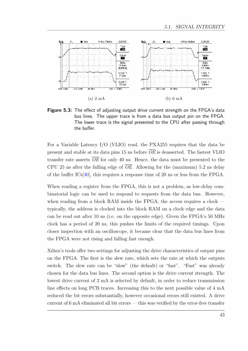
5.1. SIGNAL INTEGRITY
(a) 2 mA (b) 6 mA
Figure 5.3: The effect of adjusting output drive current strength on the FPGA’s databus lines. The upper trace is from a data bus output pin on the FPGA.The lower trace is the signal presented to the CPU after passing throughthe buffer.
For a Variable Latency I/O (VLIO) read, the PXA255 requires that the data be
present and stable at its data pins 15 ns before OE is deasserted. The fastest VLIO
transfer rate asserts OE for only 40 ns. Hence, the data must be presented to the
CPU 25 ns after the falling edge of OE. Allowing for the (maximum) 5.2 ns delay
of the buffer ICs[40], this requires a response time of 20 ns or less from the FPGA.
When reading a register from the FPGA, this is not a problem, as low-delay com-
binatorial logic can be used to respond to requests from the data bus. However,
when reading from a block RAM inside the FPGA, the access requires a clock —
typically, the address is clocked into the block RAM on a clock edge and the data
can be read out after 10 ns (i.e. on the opposite edge). Given the FPGA’s 50 MHz
clock has a period of 20 ns, this pushes the limits of the required timings. Upon
closer inspection with an oscilloscope, it became clear that the data bus lines from
the FPGA were not rising and falling fast enough.
Xilinx’s tools offer two settings for adjusting the drive characteristics of output pins
on the FPGA. The first is the slew rate, which sets the rate at which the outputs
switch. The slew rate can be “slow” (the default) or “fast”. “Fast” was already
chosen for the data bus lines. The second option is the drive current strength. The
lowest drive current of 2 mA is selected by default, in order to reduce transmission
line effects on long PCB traces. Increasing this to the next possible value of 4 mA
reduced the bit errors substantially, however occasional errors still existed. A drive
current of 6 mA eliminated all bit errors — this was verified by the error-free transfer
43

CHAPTER 5. DESIGN EVALUATION
Figure 5.4: Overshoot on the PWE signal.
of 100 GB of data.
The impact of adjusting the drive current on rise/fall times is clearly visible in
Figure 5.3. In both the 2 mA and 6 mA traces, the output of the data bus buffer
(shown in the lower trace) has a sharper transition. In the 2 mA trace, this transition
occurs too late, adding several nanoseconds of delay — just enough to push the total
path delay above the minimum acceptable.
5.1.2 CPU bus control lines
Whilst inspecting the write behaviour of the data bus, one signal stood out as being
particularly unhealthy. The PWE line was the only trace to exhibit large amounts of
overshoot and ringing. As can be seen from Figure 5.4, nearly ±1.2 V of overshoot
was present on the 3.3 V signal. Given that no other signals presented such extreme
behaviour, the only reason for the PWE line to be different is its tracking on the
board.
Examining the location of the PWE trace on the PCB revealed why the signal
suffered such severe overshoot (Figure 5.5). Not only was the entire track nearly
24 cm long, but it passed over two cuts in the ground plane. The track’s length
creates a significant capacitive component, whilst passing the track over the cut
ground plane creates an significant inductance. The inductance creates the excessive
overshoot. The combination of the two creates an LC resonant circuit, leading to
the ringing observed in the oscilloscope capture.
44

5.1. SIGNAL INTEGRITY
Figure 5.5: The PWE track on the PCB is shown in red. The yellow line representsthe inductance loops created by the cuts in the ground plane.
To confirm that the poor choice of tracking really was the cause of the signal degra-
dation, some rough calculations of the expected resonant frequency of this circuit
were compared to the observed behaviour on the oscilloscope. If the inductive com-
ponent is modelled as two rectangular loops caused by the cuts in the ground plane,
and the capacitive component is modelled as a parallel plate capacitor with the area
of the PWE track, the resonant frequency can be estimated.
A track of length 240 mm, width 0.18 mm and distance 0.2 mm from the ground
plane, with a dielectric of 5ε0 can be a approximated as having 10 pF of capacitance,
ignoring fringing effects1. The two rectangular loops have dimensions 11 mm×8 mm
and 54 mm × 10 mm, giving inductances of 24 nH and 97 nH, respectively2. This
gives a period in the order of T = 2π√
LC = 7 ns.
This result is a reasonable approximation to the 15 ns period of the ringing ob-
served from the oscilloscope trace in Figure 5.4. Although this overshoot does not
noticeably degrade performance, it incurs unnecessary oxide stress within the CMOS
structures of the FPGA, USB and Ethernet devices, leading to an increased risk of
failure. On the next revision of the board, the track was re-routed to reduce the
1Fringing effects in fact have a substantial impact on the capacitance in this case, but we expectthe answer to lie within a similar order of magnitude.
2These calculations are based on a wire (return path) diameter of 14 mil (1/1000th of an inch)and a relative permeability of 1.
45

CHAPTER 5. DESIGN EVALUATION
track length and a shorter return path was added for the signal.
5.1.3 SRAM interface
The interface between the SRAM and FPGA operates flawlessly at 50 MHz. How-
ever, both the SRAM and FPGA are capable of operating at up to 100 MHz. By
clocking the SRAM interface at a faster rate than the rest of the FPGA, no single
component inside the FPGA can saturate the SRAM bus. This is highly bene-
ficial as memory bandwidth-intensive operations, such as FFTs and stereo vision
algorithms, can operate without starving a camera supplying frames or the CPU
reading results.
Inside the FPGA, the SRAM interface (described in more detail in [4]) is decoupled
through the use of asynchronous FIFOs to queue read and write requests. Using a
DFS (Digital Frequency Synthesizer) block, the SRAM can be operated at a range of
frequencies, achieved by multiplying and/or dividing the 50 MHz clock by integers
in the range from 2 to 32. Unfortunately, attempting to run the SRAM at 100 MHz
failed with frequent bit errors. These bit errors only occurred on reading from
SRAM; writing to the SRAM did not produce an error3.
Through experimentation, it was discovered that the fastest speed at which reads
could be achieved was 83.3 MHz. Once again, investigation of the signal lines with
an oscilloscope revealed the cause. On a 50 MHz signal, the rise and fall times of
the data bus lines for writes to the FPGA were both 4 ns. When performing reads,
the rise and fall times were measured to be 6 ns. Thus any signal that switches
faster than 16 ns+6ns
= 83.3 MHz can not be reliably guaranteed. This agrees with
the experimental results obtained.
Adjusting the output drive current strength (as was done for the CPU bus in Sec-
tion 5.1.1) offers no benefit, as it does not influence the SRAM’s output characteris-
tics. Instead, the capacitance of the tracks would need to be reduced by shortening
the traces, avoiding vias and/or rearranging the components. This was not done
due to time constraints, but should be considered in future revisions of the board.
3In order to test reading and writing independently, a known good FPGA image (operating at50 MHz) was loaded into the FPGA to perform one half of the test.
46

5.2. I/O BANDWIDTH
5.2 I/O Bandwidth
As the target application of the platform is real-time image processing, throughput
must be maximised through the critical image data paths. These paths are: from the
cameras to the FPGA; the FPGA to the CPU; and the CPU to real-world interfaces
(such as the LCD, Ethernet and USB).
The camera to FPGA interface must be designed to accommodate the pixel clock
frequency of 17.73 MHz. Past work at The University of Western Australia with
these cameras have utilised buffer chips and other circuitry for 5 V → 3.3 V level
conversion. Unfortunately, that circuitry introduced a sufficiently large reactance,
causing the signal to be degraded due to lengthy rise and fall times. Learning from
these discoveries, the EyeBot M6’s camera connections to the FPGA avoided any
intermediate circuitry, were kept close to the ground plane and as short as feasibly
possible.
The FPGA to CPU interface could be considered the most critical path on the
entire board, as the CPU is where the intelligent processing can finally begin. To
be able to transfer images in real-time to the CPU, a fast bus interface is required.
A 352×288 pixel image in 16-bit colour at 50 frames per second requires a transfer
rate of 9.67 MB/s. Ideally, the system should be capable of streaming this amount
of data constantly from the FPGA to the CPU.
Using the VLIO transfer mode of the PXA255, the theoretical upper limit on the
transfer rate over a 16-bit bus is 22.4 MB/s (see Figure 5.6). This assumes that burst
transfers are always performed (to avoid unnecessary set-up/hold delays) and does
not allow for any other devices on the bus, such as the LCD and other peripherals
which require a fixed proportion of the bus’s bandwidth.
Some empirical testing provided the results shown in Figure 5.7(a). Three different
methods for reads were trialed.
MMIO mode — Memory mapped I/O is the simplest method of data transfer.
In this mode, the CPU requests one 16-bit word at a time from the FPGA
through its memory-mapped I/O space. The CPU is unable to service any
other tasks whilst waiting for data from the FPGA, but both user-mode and
kernel-mode tasks that wish to access the FPGA require no special interface.
Each 16-bit read has configurable setup times and hold times, as documented
Section 6.7.6 of [41].
47

CHAPTER 5. DESIGN EVALUATION
20 ns
RDF+1 = 40 ns
RDN+2 = 40 ns
10 ns
2 RRR+1 = 30 ns
340 ns
MEMCLK
20 ns
RDF+1 = 40 ns
RDN+2 = 40 ns
10 ns
2 RRR+1 = 30 ns
340 ns
MEMCLK
nCS
20 ns
RDF+1 = 40 ns
RDN+2 = 40 ns
10 ns
2 RRR+1 = 30 ns
340 ns
MEMCLK
nCS
nOE
Figure 5.6: Minimum timing diagram for a VLIO burst-of-four read from the FPGA.A period of 340 ns between subsequent read requests gives a theoreticalupper limit of 8 bytes
340 ns= 22.4 MB/s on a 16-bit bus.
The values for RDF, RDN, RRR determine the timing characteristics ofVLIO accesses, and must be configured through the PXA255’s MSCx reg-isters, as per Section 6.7.3 of [41]. Above, RDF, RDN, RRR are set totheir minimum values of 3, 2 and 1, respectively.
48

5.2. I/O BANDWIDTH
DMA via kernel — Using DMA has several advantages over MMIO mode trans-
fers:
• The CPU is available to process other instructions whilst waiting for data
to arrive.
• The DMA controller is aware that multiple sequential bytes will be read,
and hence can optimise accesses using burst transfers.
• The CPU does not also have to perform the subsequent write to memory.
Transfers are performed by the DMA controller, which is external to the CPU
and has no awareness of the page translation tables in use by the CPU. Hence
all addresses used by the DMA controller must be physical memory addresses,
not virtual addresses. This means the destination pages for DMA must be
contiguous in physical memory. Only the kernel can request such pages; con-
tiguous pages in a userspace process are only contiguous in the virtual address
space and are not guaranteed contiguous in physical memory.
Due to this limitation, in order to use DMA to transfer data to userspace
applications, the data must be handled twice — once to perform the DMA
into contiguous pages accessible by the kernel and then again to copy it to
userspace. Despite this performance penalty, the speed gain is still significant
in comparison, nearly tripling the speed of MMIO mode. This speedup is
largely from the utilisation of burst transfers on the bus.
If the second copy could be avoided, throughput would be improved further.
DMA to userspace — Facilities to perform DMA to userspace have not yet en-
tered the mainstream Linux kernel, however work has been done to achieve
this on PCI-based platforms[42], seeking to be merged in the next major devel-
opment cycle of the Linux kernel. Similar ideas are being pursued to improve
the efficiency of the Linux networking stack[43], with speed improvements of
up to 80% on multi-processor machines.
A similar scheme has been used on the EyeBot M6 to provide a physically-
contiguous memory region to a userspace process that can then be used for
DMA. When such a memory region is requested, it is given two virtual address
mappings — one in the kernel’s address space (which is in-fact a 1:1 mapping
to physical RAM), and a second in the process’s own virtual memory area.
Care needs to be taken to maintain coherency with the PXA255’s data cache.
49

CHAPTER 5. DESIGN EVALUATION
MM
IO
DM
A v
ia k
erne
l
DM
A to
use
rspa
ce
The
oret
ical
lim
it0
10
20
30
Rea
d tr
ansf
er s
peed
(M
B/s
)
0
10
20
30
Rea
d tr
ansf
er s
peed
(M
B/s
)
3.6
9.4
15.6
22.4
(a) Read performanceM
MIO
DM
A v
ia k
erne
l
DM
A to
use
rspa
ce
The
oret
ical
lim
it
0
10
20
30
Writ
e tr
ansf
er s
peed
(M
B/s
)
0
10
20
30
Writ
e tr
ansf
er s
peed
(M
B/s
)
13.711.6
14.1
22.4
(b) Write performance
Figure 5.7: Empirical performance measurements using VLIO.
Caching policies are applied through the MMU’s pagetables, and hence apply
to virtual addresses. The Linux kernel’s DMA routines take care of cache co-
herency to the kernel’s virtual address mapping but not the userspace address
mapping. Thus after performing the DMA, any data cache-lines associated
with the virtual mapping must be explicitly flushed.
Empirical results (shown in Figure 5.7(a)) demonstrate DMA to userspace transfer
speeds to be 66% faster than DMA via the kernel, and more than four times as
fast as MMIO mode. Combined with the ability to perform other processing tasks
whilst waiting for data to arrive, this mode of transfer offers the optimal solution
for streaming images in real-time from the FPGA.
In Figure 5.7(b), empirical results show that writing to the FPGA is in fact faster
via MMIO than performing DMA via the kernel. This arises from two factors —
the PXA255 coalescing writes into burst transfers improving the speed of MMIO,
and the need for a second memory-to-memory copy from kernel-space into userspace
slowing down the DMA process. The speed of MMIO is not significantly slower than
direct DMA from userspace, suggesting that the extra code complexity involved in
ensuring cache coherency is not beneficial.
Further improvements in transfer speed could be achieved by utilising a bus access
method other than VLIO. This requires an extra line to be routed from the CPU
50

5.3. POWER CONSUMPTION
Component Minimum Maximum TypicalBase system 1 200 mW 2 400 mW 1 800 mWEthernet (100 Mbit) 0.4 mW 400 mW 400 mWAC97 3.3 mW 100 mW 50 mWFPGA 0 mW 855 mW 400 mWSRAM 0 mW 577 mW 400 mWCameras 0 mW 132 mW 132 mWUSB 2.0 Host 0 mW 117 mW 80 mWLCD 0 mW 77 mW 47 mWMotor Controllers 0 mW 840 mW 600 mWMotors 0 mW 10 000 mW 0 mWServos 0 mW 10 500 mW 0 mWPSDs 0 mW 1 050 mW 0 mWTotal 1 204 mW 25 848 mW 3 809 mW
Table 5.1: Estimated power consumption under stand-by conditions, worst-case condi-tions and one typical usage scenario.
to the FPGA (WE), for which there was no spare FPGA pin on the initial revision.
The second revision of the board has freed up one such pin and has the WE line
routed through, allowing the possibility for the FPGA to emulate an SRAM-like
device and further increase transfer speed.
A 32-bit data bus, rather than the chosen 16-bit bus, would precisely double the
achievable speed. However, following this path would require a larger board in
order to physically fit another 16-bit data buffer, and further complicate the already
densely routed PCB.
5.3 Power Consumption
As numerous target applications of the EyeBot M6 will be battery operated, the
ability to minimise power consumption is advantageous. Table 5.1 lists:
• the minimum power that can be drawn by each device on the board;
• the maximum power that may potentially be drawn by each device on the
board;
• empirical values of power usage, measured in one typical scenario (specifically
image-processing — no motors, servos or PSDs, but with two cameras, the
51
CHAPTER 5. DESIGN EVALUATION
FPGA, SRAM and Ethernet enabled).
Each of the components in Table 5.1 (except for the base system) can be enabled
or disabled independently, allowing for a very fine grained approach to managing
power consumption.
For minimum power consumption, all devices on the board other than the CPU must
be disabled. The 1.2 W consumed is due to the fact that the PXA255 continues
running at full speed. The PXA255 supports low-power modes which have not
been investigated, but could potentially drop power consumption to below 100 mW.
Future work will attempt to minimise the power consumption as much as possible,
and still allow the device to resume in response to interrupts.
5.4 Stereo Vision
As described in Section 3.3.2, one intention of fixing the camera positions on the
board was to coerce corresponding scan lines of the cameras to lie on epipolar lines.
This reduces the search space for stereo vision algorithms implementing area-based
matching. The premise of the model required that the cameras be manufactured
identically.
Of the cameras available, only one combination of two cameras gave results that were
close to ideal (shown in Figure 5.8). Other combinations exhibited clear differences
in the manufacturing of the camera modules. The imaging sensor on one of the
camera modules was raised slightly on an edge, and thus not coplanar with any of
the other modules. Although the other modules were coplanar, they possessed subtle
but noticable differences in their vertical offsets and rotational components. The
vertical offset can be attributed to differences in the lens mounting. The rotational
component arises from the positioning of the CCD device on the board itself.
The lack of consistency between camera modules means that a stereo vision system
must either carefully choose matched cameras or implement an initial rectification
stage to project each image into the same plane. The latter approach requires a
calibration routine to calculate the required transform. The calibration only needs
to be performed once for a given pair of cameras.
Projection into the plane is often approximated by an affine transformation. A space-
efficient implementation of an affine transformation in the FPGA could potentially
52

5.5. OPTIMISING IMAGE PROCESSING FUNCTIONS ON THE PXA255
Figure 5.8: Images of an alignment test pattern, captured simultaneously from bothcameras on the EyeBot M6.
be achieved in around 4 320 logic cells[44], or around 40% of the logic in Spartan-3E
FPGA on the EyeBot M6.
5.5 Optimising image processing functions on the PXA255
Although the main aim of this hardware platform is to remove to repetitive image
processing tasks from the CPU and implement them in the FPGA, this may not
always be feasible or desirable. For example when prototyping algorithms, writing
and verifying C code is often much quicker than the equivalent task in VHDL code.
Thus being able to improve the performance of CPU-level code is highly desirable.
Assuming that an algorithm cannot be macro-optimised any further (its complexity
is fixed), areas for micro-optimisation need to be investigated.
As discussed in Section 3.1, the PXA255 offers the ARMv5TE instruction set, with
DSP-enhancements. Many of these extra features are automatically utilised by the
GNU C compiler4. Instructions that are not quite as straight-forward for the com-
piler to optimise, such as saturating addition/subtraction or count leading zeroes,
can be utilised through the use of intrinsics. (Intrinsics allow access to architecture-
specific instructions but can be implemented in a portable fashion).
Resorting to optimisation through writing assembly code is generally undesirable,
as the code no longer remains portable and becomes harder to maintain. However,
by understanding what assembly instructions can be generated for the ARMv5TE
4The parameter -march=armv5te needs to be passed to the gcc command in order for the DSPextensions to be used.
53

CHAPTER 5. DESIGN EVALUATION
instruction set, C code can be written to encourage GCC to create more optimal
output. As an example, some basic code to apply a mask to an image was analysed.
The code in its simplest form is shown in Listing 5.1. It performs pair-wise mul-
tiplication on two 8-bit images, storing the upper 8-bits of the 16-bit result. The
compiler used was gcc 3.4.5 with optimisation level 2. The generated assembly5 has
an inner loop of 9 instructions, an outer loop of 15 instructions, and takes 8.9 ms
for a 352 × 288 image on the 400 MHz PXA255. The first observation is that the
nested loops reduce the effectiveness of the branch predictor.
void apply_mask_c_1(img_t image, img_t mask, img_t result)
int x, y;
for (y = 0; y < HEIGHT; y++)
for (x = 0; x < WIDTH; x++)
result[y][x] = ((image[y][x] * mask[y][x]) >> 8);
Listing 5.1: Code to apply a mask to an image, in its simplest unoptimised form. img tis a 2-dimensional array of 8-bit values.
By utilising the knowledge that a 2-dimensional array is stored contiguously in mem-
ory, the code can be reduced to a single loop using pointers into the array (List-
ing 5.2). The generated assembly has a single loop of 8 instructions and completes
in 8.3 ms.
void apply_mask_c_2(img_t image, img_t mask, img_t result)
int i;
u8 *p, *q, *r;
p = (u8*)image;
q = (u8*)mask;
r = (u8*)result;
for (i = 0; i < HEIGHT*WIDTH; i++)
*r++ = ((*p++) * (*q++))>>8;
Listing 5.2: Acting on the knowledge that the 2-dimensional arrays are stored contigu-ously allows one loop to be used instead of two.
By forgoing the use of a loop counter, as shown in Listing 5.3, one instruction is
5The generated assembly for all the routines in this section is included in Appendix B.
54
5.5. OPTIMISING IMAGE PROCESSING FUNCTIONS ON THE PXA255
void apply_mask_c_3(img_t image, img_t mask, img_t result)
u8 *p, *q, *r, *end;
p = (u8*)image;
q = (u8*)mask;
r = (u8*)result;
end = p + (HEIGHT*WIDTH);
while (p != end)
*r++ = ((*p++) * (*q++))>>8;
Listing 5.3: Replacing the unnecessary loop variable eliminates an instruction frominside the loop.
shaved off the size of the loop. Unfortunately, this code takes precisely the same
execution time as the previous attempt with 8 instructions in the inner loop (8.3 ms).
This is attributed to the load requiring three cycles, assuming the data to be loaded
is in the data cache. If an instruction that requires the result of a load immediately
follows, it will stall for two cycles. In this case the result of the load is used two cycles
later and hence stalls for one cycle, effectively giving the loop the same execution
time as the previous attempt.
Loop unrolling is another common technique for improving code performance, as
it avoids the penalty of branching. A compiler flag exists for gcc to perform loop
unrolling, however it does not give any benefit in this case, as the XScale’s branch
predictor already predicts the branch accurately, so no penalty is incurred. Instead,
the loop can be unrolled by hand four times in order to perform writes as 32-bit
words rather than 8-bit words. This increases the size of the loop to 20 instructions
but achieves four bytes per iteration, thus gives an average of 5 instructions per
iteration. It also requires that the destination buffer is aligned to a 4-byte boundary.
This code (shown in Listing 5.4) takes 5.0 ms per frame to execute. Performing the
loads as 32-bits offers no benefit, as more instructions are required to extract the
four 8-bit bytes than to perform the individual reads.
The PXA255 CPU will complete most data processing instructions in one clock cycle,
unless the following instruction requires the result shifted by an explicit number of
bits. If a shifted result is required in the following instruction, the instruction
pipeline will stall for one cycle waiting for the result. In the previous method, the
result was built sequentially using bit shifts at each stage, incurring pipeline stalls.
55

CHAPTER 5. DESIGN EVALUATION
void apply_mask_c_4(img_t image, img_t mask, img_t result)
u8 *p, *q, *end;
u32 *r;
p = (u8*)image;
q = (u8*)mask;
r = (u32*)result;
end = p + (HEIGHT*WIDTH);
while (end != p)
u32 res1, res2, res3, res4;
res1 = (*p++ * *q++) >> 8;
res2 = (*p++ * *q++) >> 8;
res3 = (*p++ * *q++) >> 8;
res4 = (*p++ * *q++) >> 8;
*r++ = res1 | (res2 << 8) | (res3 << 16) | (res4 << 24);
Listing 5.4: Loop unrolling to perform writes 32-bits at a time.
If instead the 32-bit result was constructed in parallel from two intermediate 16-
bit results, the linear dependency tree is removed. This spreads the dependency
requirements between registers so that the likelihood that the instruction pipeline
will stall is minimised (it is assumed that the compiler is aware of where pipeline
stalls occur and can schedule the instructions appropriately).
This code is shown in Listing 5.5. The assembly generated by this code actually has
an inner loop of 21 instructions — one instruction longer than previously, giving an
average of 5.2 instructions per iteration. However, the code executes in 4.6 ms per
frame. This is almost half the time required for the initial implementation!
These results have all been achieved without resorting to assembly code but required
examining the assembly output produced by the compiler and knowledge of the
CPU architecture. Hand-coding assembly code is not only a slow and error-prone
process, but tends to produce less efficient code unless the coder knows precisely how
to schedule instructions optimally. An assembly routine was coded to perform the
above task (apply_mask_asm_2_1, shown in Appendix B) and achieved an execution
time of 4.5 ms per frame — not significantly faster than the fully optimised C code.
The efficiency of the functions presented here are summarised in Table 5.2.
As the gcc compiler understands many of the intricacies of the XScale architecture,
56

5.5. OPTIMISING IMAGE PROCESSING FUNCTIONS ON THE PXA255
void apply_mask_c_5(img_t image, img_t mask, img_t result)
u8 *p, *q, *end;
u32 *r;
p = (u8*)image;
q = (u8*)mask;
r = (u32*)result;
end = p + (HEIGHT*WIDTH);
while (end != p)
u32 res1, res2;
res1 = *p++ * *q++;
res1 = res1 >> 8 | ((*p++ * *q++) & 0xff00);
res2 = *p++ * *q++;
res2 = res2 >> 8 | ((*p++ * *q++) & 0xff00);
*r++ = res1 | (res2 << 16);
Listing 5.5: Building the result in parallel rather than sequentially removes unnecessarypipeline stalls.
Function Time per frame % Gainapply_mask_c_1 8.9 ms 0%apply_mask_c_2 8.3 ms 7%apply_mask_c_3 8.3 ms 7%apply_mask_c_4 5.0 ms 43%apply_mask_c_5 4.6 ms 48%apply_mask_asm_2_1 4.5 ms 49%
Table 5.2: Timing and efficiency gains for various optimisations of an image maskingroutine.
it can achieve near-optimal code with substantially less effort from the programmer,
compared to writing assembly by hand. The C code also remains portable to other
architectures and platforms, whereas optimised assembly code is of no use. Thus,
optimising C code based upon knowledge of the architecture is a preferable approach
to improving execution speed6.
6Appendix A of [45] details methods of optimising assembly routines. It is targeted at developerswriting in ARM assembly and optimising compiler writers, but gives a deeper understanding ofhow an optimising compiler may be exploited to generate more efficient code.
57


Chapter 6
Conclusion
Over the course of this project, a high-performance embedded system was designed,
developed and evaluated, for the purposes of real-time image processing. The sys-
tem provides a highly adaptable hardware and software platform by combining the
parallelism of programmable logic with the versatility of a fast 32-bit RISC CPU.
Through optimising the flow of data through the system, images can be processed
efficiently in order to achieve real-time speeds.
The design was built upon the experiences of previous FPGA-based imaging devices,
and has been adapted for use as a mobile robotics platform. Two cameras were
connected directly to the FPGA, allowing stereo vision algorithms to be utilised to
achieve depth perception. In addition, power consumption was minimised through
a fine-grained power management scheme.
The performance of the design was analysed in order to improve the speed of data
transfers. Techniques were also explored for improving the efficiency of image-
processing code. Together, the system’s resources are effectively utilised to maximise
throughput from end to end.
It is hoped that this platform will serve the needs of high-performance image pro-
cessing applications for many years to come.
6.1 Future Work
Creating or adapting an appropriate hardware platform is often the a very time-
consuming task for an embedded image-processing project. As the EyeBot M6
59

CHAPTER 6. CONCLUSION
provides a system tailored for image processing, it can serve as the starting point
for a vast range of computer vision-related projects.
The next step in making hardware image processing easily accessible, is the cre-
ation of a library of pluggable VHDL image processing routines. This allows a user
to request images from the camera that have already had a set of transformations
applied. The Xilinx tools offer a graphical block-level editor, allowing VHDL com-
ponents to be connected on-screen to form a single FPGA programming image. This
method could potentially be used to graphically connect a sequence of image pro-
cessing components together, requiring no knowledge of VHDL or the underlying
system.
As the successor to previous EyeBot generations, a port of the RoBIOS operating
system will be completed to allow existing applications to run unmodified. RoBIOS
provides a standardised interface to motors, servos, quadrature encoders, position
sensing devices and other hardware devices commonly found on robotic platforms.
It also offers high-level control functions for navigation and motor control.
Further work to be performed on the platform includes:
User interface — a light-weight toolkit with touchscreen support needs to be writ-
ten or adapted to the EyeBot M6. A facility to export the user interface over
the network using a remote desktop protocol such as RDP or VNC would allow
a portable method of remotely controlling the EyeBot.
Application interface — a simple, documented method of loading user applica-
tions onto the device over USB to make life easier for application developers.
FPGA I/O standardisation — the devices attached to the FPGA (such as mo-
tors, servos, and PSDs) require standardised addresses for libM6 to access. A
definitive bitstream providing access to all devices on the FPGA needs to be
created and versioned.
ISP1761 bug — isolating the ISP1761 interrupt bug described in Section 4.1.2.
Additional areas that could be explored on the platform include:
Real-time Linux — for more complicated control applications where bounded de-
terminism is mandatory, a real-time operating system is required. Real-time
60
6.1. FUTURE WORK
ports of the Linux kernel are available, but drivers will need to ensure they do
not interfere with the operation of the real-time scheduler.
Improving performance using non-VLIO transfers — the second revision of
the board will give the FPGA access to the PXA255’s WE signal, allowing
transfers to be performed with faster transfer modes than VLIO.
Partial reconfiguration — the board has signals connected that potentially al-
low partial reconfiguration to be performed. Partial reconfiguration could be
used to transparently change image processing algorithms without affecting
operation of the rest of the device.
Power consumption — although all peripherals on the board can be disabled,
the PXA255 CPU itself never enters a low-power mode. The PXA255 offers a
rich set of power-saving modes. Investigating these may allow the EyeBot M6
to remain in standby for over a week. Driver support for suspend/resume will
constitute a large portion of this work.
The development of the EyeBot M6 has opened up a world of possibilities for easily
experimenting with embedded vision systems, limited only by one’s creativity and
imagination1. Building up a library of reusable software and VHDL components will
accelerate the development of future systems, allowing the rapid creation of a wide
variety of applications. This project has laid down the foundations for autonomous
robots, vehicles, submarines and other devices to benefit from a powerful imaging
system.
1. . . and the size of the FPGA.
61


Appendix A
Board Detail
A.1 Power Control Signals
Signal Connected to Purpose
PWRON PXA255 GPIO32 When high, keeps the main regulator powered.
5VEN AC97 GPIO2 When high, supplies 5 V power to the motor drivers,
servos and USB ports.
PWFPGA AC97 GPIO0 When high, enables the 2.5 V and 1.2 V power sup-
plies for the FPGA, and the 50 MHz crystal.
FCFG AC97 GPIO9 When high, sinks 30 mA of current from the 2.5 V
rail — must be high when programming the FPGA.
FROFF FPGA P144 When high, disables the SRAM.
PWOFF AC97 GPIO5 When high, disables Camera 1 and places the SRAM
into standby.
CAMOFF AC97 GPIO4 When high, disables Camera 2
63

APPENDIX A. BOARD DETAIL
A.2 Top view
A.2.1 Jumpers
J8 On: connect RTS pin of Serial 2 to 5 V
J9 On: connect RTS pin of Serial 1 to 5 V
J12 On: disable console on Serial 1
J35 Composite Video output from Camera 1
J36 Composite Video output from Camera 2
A.2.2 Top board connector pinout
Microphone Input 1 2 Microphone Ground
Speaker Output 3 4 Analog Ground
5 V 5 6 Ground
VBATT 7 8 3.3 V
Digital I/O 0 9 10 Digital I/O 1
Digital I/O 2 11 12 Digital I/O 3
Digital I/O 4 13 14 Digital I/O 5
Digital I/O 6 15 16 AC97 Sync
Infrared Signal 17 18 AC97 Reset
ADC synchroniser 19 20 AC97 Bit Clock
AC97 Data In 21 22 AC97 Data Out
I2C Serial Clock 23 24 I2C Serial Data
Touchscreen X+ 25 26 Touchscreen Y+
Touchscreen X- 27 28 Touchscreen Y-
Power Supply Hold 29 30 Serial 2 Rx
Serial Console Enable 31 32 Serial 2 Tx
Slave USB- 33 34 Serial 1 Rx
Slave USB+ 35 36 Serial 1 Tx
64

A.2. TOP VIEW
Pin 1 of the camera module is marked “Y0”.Cameras hang below the board when mounted.
65

APPENDIX A. BOARD DETAIL
A.3 Bottom view
66

A.3. BOTTOM VIEW
A.3.1 Connectors
JP1 — Test points
Warning: Do not pull up/down these signals without a series resistor.
1 Pull high to force FPGA power on (1.2 V and 2.5 V rails)
2 3.3 V
3 Ground
4 3.3 V
5 Pull high to force 5 V line
6 3.3 V
7 Pull high to force power circuity to stay on
8 3.3 V
9 VBATT
10 Ground
11 Connected to power button
12 5 V
13 2.5 V
14 Ground
15 1.2 V
16 Ground
JP2, JP3 — Motor power
JP2 controls the power source for motors 1 and 2. JP3 controls the power source
for motors 3 and 4. Both have the following pinout:
1 5 V
2 Motor power
3 VBATT
Thus a jumper from pin 1-2 will supply 5 V to the motors, and a jumper from pin
2-3 will supply the battery voltage to the motors. Alternately, an external supply
can be connected to pin 2. Ensure that this supply is within the specifications of
the L293DD motor driver IC.
67

APPENDIX A. BOARD DETAIL
J30–33 — Motors
1 Motor -
2 Motor +
3 Ground
4 VCC (5V)
5 Encoder B
6 Encoder A
J14–20 — Servos
1 Signal
2 5 V
3 Ground
J24–26 — PSDs
1 Ground
2 Clock Input
3 5 V
4 Data Output
J5 — ADC Inputs
1 5 V
2 Analog Input 0
3 Analog Input 1
4 Analog Input 2
5 Analog Ground
J34 — Digital I/O
The digital I/O pins are divided into two banks of 8 pins each. Each set of 8 are be
configured to be simultaneously inputs or outputs.
3.3 V 1 2 5V
DIO 0/0 3 4 DIO 0/1
DIO 0/2 5 6 DIO 0/3
DIO 0/4 7 8 DIO 0/5
DIO 0/6 9 10 DIO 0/7
DIO 1/0 11 12 DIO 1/1
DIO 1/2 13 14 DIO 1/3
DIO 1/4† 15 16 DIO 1/5†DIO 1/6† 17 18 DIO 1/7†
Ground 19 20 Ground
† These I/O lines are shared with Camera 2 and are not available if Camera 2 is in use.
68

A.3. BOTTOM VIEW
P3 — USB Port
This port is designed to connect to a standard USB port cable, as found inside PC
motherboards.
1 Ground
2 Data -
3 Data +
4 5 V
69


Appendix B
Assembly Listings for Section 5.5
000001d0 <apply_mask_c_1>:
1d0: e92d40f0 stmdb sp!, r4, r5, r6, r7, lr
1d4: e3a0e000 mov lr, #0 ; 0x0
1d8: e1a06000 mov r6, r0
1dc: e1a05001 mov r5, r1
1e0: e1a04002 mov r4, r2
1e4: e1a0000e mov r0, lr
1e8: e59f7038 ldr r7, [pc, #56] ; 228 <.text+0x228>
1ec: e3a0c000 mov ip, #0 ; 0x0
1f0: e080200c add r2, r0, ip
1f4: e7d21006 ldrb r1, [r2, r6]
1f8: e7d23005 ldrb r3, [r2, r5]
1fc: e28cc001 add ip, ip, #1 ; 0x1
200: e15c0007 cmp ip, r7
204: e0030391 mul r3, r1, r3
208: e1a03443 mov r3, r3, asr #8
20c: e7c23004 strb r3, [r2, r4]
210: dafffff6 ble 1f0 <apply_mask_c_1+0x20>
214: e28ee001 add lr, lr, #1 ; 0x1
218: e35e0e12 cmp lr, #288 ; 0x120
21c: e2800e16 add r0, r0, #352 ; 0x160
220: bafffff0 blt 1e8 <apply_mask_c_1+0x18>
224: e8bd80f0 ldmia sp!, r4, r5, r6, r7, pc
71

APPENDIX B. ASSEMBLY LISTINGS FOR SECTION ??
228: 0000015f andeq r0, r0, pc, asr r1
0000022c <apply_mask_c_2>:
22c: e92d4010 stmdb sp!, r4, lr
230: e59f4028 ldr r4, [pc, #40] ; 260 <.text+0x260>
234: e1a0e002 mov lr, r2
238: e3a0c000 mov ip, #0 ; 0x0
23c: e4d02001 ldrb r2, [r0], #1
240: e4d13001 ldrb r3, [r1], #1
244: e28cc001 add ip, ip, #1 ; 0x1
248: e15c0004 cmp ip, r4
24c: e0030392 mul r3, r2, r3
250: e1a03443 mov r3, r3, asr #8
254: e4ce3001 strb r3, [lr], #1
258: dafffff7 ble 23c <apply_mask_c_2+0x10>
25c: e8bd8010 ldmia sp!, r4, pc
260: 00018bff streqd r8, [r1], -pc
00000264 <apply_mask_c_3>:
264: e52de004 str lr, [sp, #-4]!
268: e1a0c002 mov ip, r2
26c: e280eb63 add lr, r0, #101376 ; 0x18c00
270: e4d02001 ldrb r2, [r0], #1
274: e4d13001 ldrb r3, [r1], #1
278: e15e0000 cmp lr, r0
27c: e0030392 mul r3, r2, r3
280: e1a03443 mov r3, r3, asr #8
284: e4cc3001 strb r3, [ip], #1
288: 1afffff8 bne 270 <apply_mask_c_3+0xc>
28c: e49df004 ldr pc, [sp], #4
72

00000290 <apply_mask_c_4>:
290: e92d40f0 stmdb sp!, r4, r5, r6, r7, lr
294: e1a04000 mov r4, r0
298: e1a05001 mov r5, r1
29c: e1a06002 mov r6, r2
2a0: e2807b63 add r7, r0, #101376 ; 0x18c00
2a4: e4d42001 ldrb r2, [r4], #1
2a8: e4d53001 ldrb r3, [r5], #1
2ac: e4d40001 ldrb r0, [r4], #1
2b0: e4d51001 ldrb r1, [r5], #1
2b4: e00e0293 mul lr, r3, r2
2b8: e4d4c001 ldrb ip, [r4], #1
2bc: e4d52001 ldrb r2, [r5], #1
2c0: e0030091 mul r3, r1, r0
2c4: e4d40001 ldrb r0, [r4], #1
2c8: e4d51001 ldrb r1, [r5], #1
2cc: e002029c mul r2, ip, r2
2d0: e0010190 mul r1, r0, r1
2d4: e1a02442 mov r2, r2, asr #8
2d8: e2033cff and r3, r3, #65280 ; 0xff00
2dc: e183342e orr r3, r3, lr, lsr #8
2e0: e1a01441 mov r1, r1, asr #8
2e4: e1833802 orr r3, r3, r2, lsl #16
2e8: e1833c01 orr r3, r3, r1, lsl #24
2ec: e1570004 cmp r7, r4
2f0: e4863004 str r3, [r6], #4
2f4: 1affffea bne 2a4 <apply_mask_c_4+0x14>
2f8: e8bd80f0 ldmia sp!, r4, r5, r6, r7, pc
73
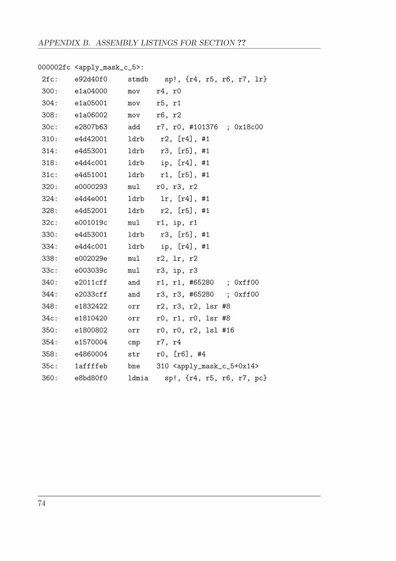
APPENDIX B. ASSEMBLY LISTINGS FOR SECTION ??
000002fc <apply_mask_c_5>:
2fc: e92d40f0 stmdb sp!, r4, r5, r6, r7, lr
300: e1a04000 mov r4, r0
304: e1a05001 mov r5, r1
308: e1a06002 mov r6, r2
30c: e2807b63 add r7, r0, #101376 ; 0x18c00
310: e4d42001 ldrb r2, [r4], #1
314: e4d53001 ldrb r3, [r5], #1
318: e4d4c001 ldrb ip, [r4], #1
31c: e4d51001 ldrb r1, [r5], #1
320: e0000293 mul r0, r3, r2
324: e4d4e001 ldrb lr, [r4], #1
328: e4d52001 ldrb r2, [r5], #1
32c: e001019c mul r1, ip, r1
330: e4d53001 ldrb r3, [r5], #1
334: e4d4c001 ldrb ip, [r4], #1
338: e002029e mul r2, lr, r2
33c: e003039c mul r3, ip, r3
340: e2011cff and r1, r1, #65280 ; 0xff00
344: e2033cff and r3, r3, #65280 ; 0xff00
348: e1832422 orr r2, r3, r2, lsr #8
34c: e1810420 orr r0, r1, r0, lsr #8
350: e1800802 orr r0, r0, r2, lsl #16
354: e1570004 cmp r7, r4
358: e4860004 str r0, [r6], #4
35c: 1affffeb bne 310 <apply_mask_c_5+0x14>
360: e8bd80f0 ldmia sp!, r4, r5, r6, r7, pc
74

Hand coded assembly version of apply_mask:
.type apply_mask_asm_2_1, %function
.global apply_mask_asm_2_1 apply_mask_asm_2_1:
stmfd sp!, r4-r9, lr
mov ip, r2
add lr, r2, #(352*288)
1:
ldrb r2, [r0], #1
ldrb r3, [r1], #1
ldrb r4, [r0], #1
ldrb r5, [r1], #1
ldrb r6, [r0], #1
ldrb r7, [r1], #1
ldrb r8, [r0], #1
ldrb r9, [r1], #1
smulbb r2, r2, r3
smulbb r4, r4, r5
smulbb r6, r6, r7
smulbb r8, r8, r9
cmp lr, ip
and r8, r8, #0xff00
and r4, r4, #0xff00
orr r8, r8, r6, asr #8
orr r4, r4, r2, asr #8
orr r2, r4, r8, asl #16
strne r2, [ip], #4
bne 1b
ldmia sp!, r4-r9, pc
75

Appendix C
libM6
libM6 is a library for accessing the hardware on the Eyebot M6. The devices con-
nected to the FPGA are depending on the correct FPGA image being loaded, and
has not yet been finalised. The documentation below covers the essential functions
for accessing the FPGA, and other existing functions.
Accessing the FPGA
volatile u16* FPGA map(FPGA addr t address, unsigned long bytes)
Maps a region of the FPGA’s address lines into the calling process’s address
space. It returns a pointer to a the memory-mapped I/O region, which should
only be accessed on 16-bit boundaries.
address is the offset into the FPGA’s address space. This should always be
an even address, as the lowest address bit is not connected to the FPGA.
bytes is the number of bytes to be mapped. This will automatically be
rounded up to the next multiple of a page size (4K bytes).
int FPGA memcpy from(void *dest, FPGA addr t src, int bytes)
Performs a DMA read from the FPGA’s address space into a memory location.
It returns 0 on success, and -1 on error (error in errno).
dest is the target address to copy data into. It must be aligned to an 8-byte
boundary.
77

APPENDIX C. LIBM6
src is the I/O address on the FPGA to copy data from. It must be aligned
to an 8-byte boundary.
bytes is the number of bytes to copy. It must be a multiple of 8.
int FPGA memcpy to(FPGA addr t src, void *src, int bytes)
Performs a DMA write to the FPGA’s address space from a memory location.
It returns 0 on success, and -1 on error (error in errno).
dest is the I/O address on the FPGA to copy data to. It must be aligned to
an 8-byte boundary.
src is the source address to copy data from. It must be aligned to an 8-byte
boundary.
bytes is the number of bytes to copy. It must be a multiple of 8.
GPIO access
int GPIO set bank direction(int bank, GPIO dir t direction)
Sets the direction of a bank of GPIO pins.
bank is 0 or 1.
direction is one of GPIO_IN or GPIO_OUT.
int GPIO set state(int bank, int gpio, int state)
Sets the state of a given GPIO pin that has been configured as an output.
bank is 0 or 1.
gpio is between 0 and 7, inclusive.
state must be 0 for clear, or non-zero for set.
int GPIO get state(int bank, int gpio)
Returns the state of a given GPIO pin that has been configured as an input.
bank is 0 or 1.
gpio is between 0 and 7, inclusive.
78

Position Sensing Devices
void PSD enable()
Enables all PSDs.
void PSD disable()
Disables all PSDs.
void PSD set update period(int ms)
Sets the number of milliseconds between PSD updates. The minimum sam-
pling interval is 83 ms. ms will be rounded up to the next multiple of the
minimum sampling interval. The default period is 83 ms.
void PSD read(int number)
Returns the uncalibrated 8-bit value read from the PSD counter.
number is between 0 and 5, inclusive.
79


References
[1] Intel Corporation, “Enhanced host controller interface for univeral serial bus.”
http://www.intel.com/technology/usb/ehcispec.htm. [On-line, accessed
15-Oct-2006].
[2] OmniVision, “OmniVision serial camera control bus (SCCB) functional specifi-
cation.” http://www.ovt.com/products/SCCBSpec AN 2 1.pdf. [On-line, ac-
cessed 10-Jul-2006].
[3] L. Chin, “FPGA-based embedded vision systems.” Final Year Project Thesis,
2006. School of Electrical, Electronic and Computer Engineering, The Univer-
sity of Western Australia.
[4] D. English, “FPGA-based embedded stereovision algorithms.” Final Year
Project Thesis, 2006. School of Electrical, Electronic and Computer Engi-
neering, The University of Western Australia.
[5] “Directive 2002/95/EC of the European Parliament and of the Council of 27
January 2003 on the restriction of the use of certain hazardous substances in
electrical and electronic equipment,” in Official Journal of the European Union,
pp. 37/19–37/21, 2003.
[6] V. Narayanan and Y. Xie, “Reliability concerns in embedded system designs,”
Computer, vol. 39, no. 1, pp. 118–120, 2006.
81
REFERENCES
[7] C.-C. Lee, I.-C. K. Chen, and T. N. Mudge, “The bi-mode branch predictor,” in
MICRO 30: Proceedings of the 30th annual ACM/IEEE international sympo-
sium on Microarchitecture, (Washington, DC, USA), pp. 4–13, IEEE Computer
Society, 1997.
[8] S. Pasricha and A. Veidenbaum, “Improving branch prediction accuracy in
embedded processors in the presence of context switches,” in Proceedings of the
21st International Conference on Computer Design, (Washington, DC, USA),
IEEE Computer Society, 2003.
[9] M. Duranton, “The challenges for high performance embedded systems,” in
Proceedings of the 9th EUROMICRO Conference on Digital System Design,
(Los Alamitos, CA, USA), IEEE Computer Society, 2006.
[10] J. Backus, “Can programming be liberated from the von Neumann style?: a
functional style and its algebra of programs,” Communications of the ACM,
vol. 21, no. 8, pp. 613–641, 1978.
[11] C. Zinner and W. Kubinger, “ROSDMA: A DMA double buffering method for
embedded image processing with resource optimized slicing,” in Proceedings
of the Twelfth IEEE Real-Time and Embedded Technology and Applications
Symposium, IEEE Computer Society, 2006.
[12] P. A. Laplante, Real-time Systems Design and Analysis: An Engineer’s Hand-
book. IEEE Press, 2 ed., 1997.
[13] J. Greco, “Parallel image processing and computer vision architecture,” 2005.
[14] P. McCurry, F. Morgan, and L. Kilmartin, “Xilinx FPGA implementation of a
pixel processor for object detection applications.”
82
REFERENCES
[15] M. Venkatesan and D. V. Rao, “An efficient reconfigurable architecture and
implementation of edge detection algorithm using Handle-C,” in ITCC ’04:
Proceedings of the International Conference on Information Technology: Coding
and Computing (ITCC’04) Volume 2, (Washington, DC, USA), p. 846, IEEE
Computer Society, 2004.
[16] S. M. Smith and J. M. Brady, “SUSAN — a new approach to low level image
processing,” Int. J. Comput. Vision, vol. 23, no. 1, pp. 45–78, 1997.
[17] C. Torres-Huitzil and M. Arias-Estrada, “An FPGA architecture for high speed
edge and corner detection,” in CAMP ’00: Proceedings of the Fifth IEEE
International Workshop on Computer Architectures for Machine Perception
(CAMP’00), (Washington, DC, USA), p. 112, IEEE Computer Society, 2000.
[18] T. H. Drayer, J. G. Tront, R. W. Conners, and P. A. Araman, “A develop-
ment system for creating real-time machine vision hardware using field pro-
grammable gate arrays,” in HICSS ’99: Proceedings of the Thirty-Second An-
nual Hawaii International Conference on System Sciences-Volume 3, (Wash-
ington, DC, USA), p. 3046, IEEE Computer Society, 1999.
[19] Z. Guo, W. Najjar, F. Vahid, and K. Vissers, “A quantitative analysis of the
speedup factors of FPGAs over processors,” in FPGA ’04: Proceedings of the
2004 ACM/SIGDA 12th International Symposium on Field Programmable Gate
Arrays, (New York, NY, USA), pp. 162–170, ACM Press, 2004.
[20] T. W. Griffin and N. L. Passos, “An experiment with hardware implementation
of edge enhancement filter,” J. Comput. Small Coll., vol. 17, no. 5, pp. 24–31,
2002.
[21] T. S. Mohamed and W. Badawy, “Integrated hardware-software platform for
image processing applications,” in Proceedings of the 4th IEEE International
83

REFERENCES
Workshop on System-on-Chip for Real-Time Applications, (Washington, DC,
USA), pp. 145–148, IEEE Computer Society, 2004.
[22] J. Villasenor, C. Jones, and B. Schoner, “Video communications using rapidly
reconfigurable hardware,” in IEEE Transactions on Circuits and Systems for
Video Technology, vol. 5, December 1995.
[23] G. Wigley and D. Kearney, “The first real operating system for reconfigurable
computers,” in Proceedings of the 6th Australasian Computer Systems Archi-
tecture Conference, (Los Alamitos, CA, USA), p. 130, IEEE Computer Society,
2001.
[24] O. Diessel, H. ElGindy, M. Middendorf, H. Schmeck, and B. Schmidt, “Dynamic
scheduling of tasks on partially reconfigurable FPGAs,” in IEEE Proceedings
of Computers and Digital Techniques, 2000.
[25] T. Braunl, “EyeBot: A family of autonomous robots,” in Proceedings of the
6th International Conference on Neural Information Processing, pp. 645–649a,
1999.
[26] A. Rowe, C. Rosenberg, and I. Nourbakhsh, “A low cost embedded color vision
system,” in Proceedings of the 2002 IEEE/RSJ International Conference on
Intelligent Robots and System, vol. 1, pp. 208–213, IEEE Computer Society,
2002.
[27] A. Rowe, C. Rosenberg, and I. Nourbakhsh, “A second generation low cost
embedded color vision system,” in Proceedings of the 2005 IEEE International
Conference on Computer Vision and Pattern Recognition, IEEE Computer So-
ciety, 2005.
84

REFERENCES
[28] Newton Laboratories, “Cognachrome image capture device.” http://www.
newtonlabs.com/. [On-line, accessed 15-Oct-2006].
[29] P. Fidler, T. Froggatt, M. Morley, A. Green, E. Greveson, and P. Long, “MDP
balloon board: An open source software & hardware system for education,” in
Proceedings of the 7th Real-time Linux Workshop, 2005.
[30] H. Francis, “ARM DSP-enhanced extensions.” http://www.arm.com/pdfs/
ARM-DSP.pdf. [On-line, accessed 14-Oct-2006].
[31] Altera Corporation, “The truth about die size: Comparing Stratix & Virtex-
II Pro FPGAs.” http://www.altera.com/literature/wp/wp stx compare.
pdf. [On-line, accessed 14-Sep-2006].
[32] Altera Corporation, “An analytical review of FPGA logic efficiency in Stratix,
Virtex-II & Virtex-II Pro devices.” http://www.altera.com/literature/wp/
wp stx logic efficiency.pdf. [On-line, accessed 14-Sep-2006].
[33] H. Patel, “The 40% performance advantage of Virtex-II Pro FPGAs over com-
petitive PLDs.” http://www.xilinx.com/bvdocs/whitepapers/wp206.pdf.
[On-line, accessed 14-Sep-2006].
[34] Philips Semiconductors, “The I2C bus specification.” http://www.nxp.com/
acrobat download/literature/9398/39340011.pdf. [On-line, accessed 4-
Oct-2006].
[35] D. A. Forsyth and J. Ponce, Computer Vision: A Modern Approach, pp. 235–
237. Prentice-Hall, 2003.
[36] Compaq, HP, Intel, Lucent, Microsoft, NEC, Philips, “Universal Serial Bus
specification, revision 2.0.” http://www.usb.org/developers/docs/. [On-
line, accessed 10-Oct-2006].
85

REFERENCES
[37] Philips Semiconductors, “Interfacing the ISP176x to the Intel PXA25x proces-
sor.” http://www.nxp.com/acrobat download/applicationnotes/AN10037
4.pdf. [On-line, accessed 10-Sep-2006].
[38] P. Alfke and B. New, “Quadrature phase decoder.” http://direct.xilinx.
com/bvdocs/appnotes/xapp012.pdf. [On-line, accessed 29-Sep-2006].
[39] K. Chapman, “Rotary encoder interface for Spartan-3E starter
kit.” http://www.xilinx.com/products/boards/s3estarter/files/
s3esk rotary encoder interface.pdf. [On-line, accessed 18-Jul-2006].
[40] Pericom Semiconductor Corporation, “PI74LPT16245 technical datasheet.”
http://www.pericom.com/pdf/datasheets/PI74LPT16245.pdf. [On-line, ac-
cessed 22-Oct-2006].
[41] Intel Corporation, “Intel PXA255 processor: Developer’s manual.”
http://www.intel.com/design/pca/applicationsprocessors/manuals/
278693.htm. [On-line, accessed 10-Oct-2006].
[42] P. Chubb, “Linux kernel infrastructure for user-level device drivers,” in
Linux.conf.au Adelaide, Australia, 2004. http://www.ertos.nicta.com.au/
publications/papers/Chubb 04.pdf [On-line, accessed 14-Sep-2006].
[43] V. Jacobson and B. Felderman, “Speeding up networking,” in Linux.conf.au
Dunedin, New Zealand, 2006. http://www.lemis.com/grog/Documentation/
vj/lca06vj.pdf [On-line, accessed 14-Sep-2006].
[44] F. Bensaali, A. Amira, I. Uzun, and A. Ahmedsaid, “An FPGA implementation
of 3D affine transformations,” in Proceedings of the 10th IEEE International
Conference on Electronics, 2003.
86

REFERENCES
[45] Intel Corporation, “Intel XScale microarchitecture for the PXA255
processor.” http://www.intel.com/design/pca/applicationsprocessors/
manuals/278693.htm. [On-line, accessed 20-Oct-2006].
87