xiang yang kong and zhong lin wang- spontaneous polarization-induced nanohelixes, nanosprings, and...
TRANSCRIPT
8/3/2019 Xiang Yang Kong and Zhong Lin Wang- Spontaneous Polarization-Induced Nanohelixes, Nanosprings, and Nanorings …
http://slidepdf.com/reader/full/xiang-yang-kong-and-zhong-lin-wang-spontaneous-polarization-induced-nanohelixes 1/7
Spontaneous Polarization-InducedNanohelixes, Nanosprings, andNanorings of Piezoelectric Nanobelts
Xiang Yang Kong and Zhong Lin Wang*
School of Materials Science and Engineering, Georgia Institute of Technology,
Atlanta, Georgia 30332-0245
Received July 1, 2003
ABSTRACT
Growth of (0001) facet-dominated, free-standing, piezoelectric zinc oxide (ZnO) nanostructures is challenged by the divergence of the surface
energy due to intrinsic polarization. By controlling growth kinetics, we show the success of growing nanobelt-based novel structures whose
surfaces are dominated by the polarized ±(0001) facets. Owing to the positive and negative ionic charges on the zinc- and oxygen-terminated±(0001) surfaces, respectively, a spontaneous polarization is induced across the nanobelt thickness. As a result, right-handed helical
nanostructures and nanorings are formed by rolling up single-crystal nanobelts; this phenomenon is attributed to a consequence of minimizing
the total energy contributed by spontaneous polarization and elasticity. The polar-surface-dominated ZnO nanobelts are likely to be an ideal
system for understanding piezoelectricity and polarization-induced ferroelectricity at nanoscale; and they could have applications as one-
dimensional nanoscale sensors, transducers, and resonators.
Zinc oxide (ZnO) is a versatile smart material that has key
applications in catalysts, sensors, piezoelectric transducers,1
transparent conductors,2 and surface acoustic wave devices.3
The noncentral symmetry and the tetrahedral coordinated
ZnO4 unit in ZnO result in anisotropic piezoelectric proper-
ties. Structurally, the wurtzite structured ZnO crystal isdescribed schematically as a number of alternating planes
composed of four-fold coordinated O2- and Zn2+ ions,
stacked alternatively along the c-axis. The oppositely charged
ions produce positively charged (0001)-Zn and negatively
charged (0001h)-O polar surfaces, resulting in a normal dipole
moment and spontaneous polarization as well as a divergence
in surface energy. To maintain a stable structure, the polar
surfaces generally have facets or exhibit massive surface
reconstructions, but ZnO ( (0001) is an exception, which
is atomically flat, stable, and without reconstruction.4,5
Understanding the superior stability of the ZnO ( (0001)
polar surfaces is a forefront research in today’s surface
physics.6-9
Nanowire- and nanotube-based materials have been dem-
onstrated as building blocks for nanocircuits, nanosystems,10-14
and nanooptoelectronics,15 and they have been fabricated for
a wide range of materials from metals, semiconductors, and
oxides to polymers.16 A variety of quasi-one-dimensional
ZnO nanostructures, such as nanowires17 and nanobelts,18
have been synthesized, and they have been used for fabricat-
ing nanoscale lasers,17 field effect transistors,19 gas sensors,20
cantilevers,21 and resonators.22 But these ZnO nanostructures
grow along the c-axis, and the side surfaces are {011h0} and
{21h 1h0} due to their energies which are lower than that of
(0001), resulting in vanishing dipole moment and much
reduced piezoelectricity. The most desirable morphology to
maximize the piezoelectric effect is to create nanostructuresthat preserve large area (0001) polar surfaces.23,24 However,
ZnO (0001) has a surface energy that diverges with sample
size due to the surface polarization charge. Therefore, growth
of (0001) surface-dominated free-standing nanostructures
needs to oVercome the barrier of surface energy.
In this paper, we report the free-standing ZnO nanobelts
that grow along the a-axis, and their large top and bottom
surfaces are the polar (0001) facets. Due to the small
thickness of the nanobelts, spontaneous polarization normal
to the nanobelt leads to the growth of helical nanostructures.
The mechanism for the helical growth is attributed to a
consequence of minimizing the total energy contributed by
spontaneous polarization and elasticity. The ZnO nanostruc-
tures have potential applications as nanoscale sensors,
resonators, and transducers that could serve as functional
components to be integrated in micro- and nanoelectrome-
chanical systems (MEMS, NEMS). They are also ideal
systems for understanding piezoelectric effect and spontane-
ous polarization induced ferroelectric effect at the nanoscale.
The structurally controlled, high-purity and high-yield ZnO
nanobelts were synthesized by a solid-vapor process.25 Zinc
oxide powders (purity 99.99%, melting point 1975 °C) were* Corresponding author. E-mail: [email protected].
NANO
LETTERS
2003Vol. 3, No. 12
1625-1631
10.1021/nl034463p CCC: $25.00 © 2003 American Chemical SocietyPublished on Web 08/06/2003
8/3/2019 Xiang Yang Kong and Zhong Lin Wang- Spontaneous Polarization-Induced Nanohelixes, Nanosprings, and Nanorings …
http://slidepdf.com/reader/full/xiang-yang-kong-and-zhong-lin-wang-spontaneous-polarization-induced-nanohelixes 2/7
placed at the highest temperature zone of a horizontal tube
furnace. Before heating to the desired temperature of 1350
°C, the tube furnace was evacuated to ∼10-3 Torr to remove
the residual oxygen. Then the source materials were heated
to 1350 °C at a heating rate of 20 °C/min. ZnO decomposes
into Zn2+ and O2- at high temperature (1350 °C) and low
pressure (∼10-3 Torr),26 and this decomposition process is
the key step for controlling the anisotropic growth of thenanobelts. After a few minutes of evaporation and decom-
position, the Ar carrier gas was introduced at a flux of 25
sccm (standard cubic centimeters per minute). The synthesis
process was conducted at 1350 °C for 30 min. The nanobelts
were deposited onto an alumina substrate placed in a
temperature zone of 400-500 °C under Ar pressure of 250
Torr. Structures of the ZnO nanobelts were analyzed by
scanning electron microscopy (SEM) and high-resolution
transmission electron microscopy (HRTEM).27
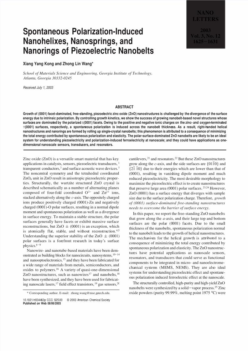
SEM and TEM analysis shows that the as-prepared product
has a belt-shape with widths of 10-60 nm, thickness of 5-20
nm and lengths up to several hundreds of micrometers. The
dominant component of the as-synthesized sample is nano-
belts with a uniform size distribution, but a significant
amount of nanobelts has ring shape (as indicated by
arrowheads in Figure 1), which has not been found for single-
crystal nanobelts or nanowires of any other materials.
The ZnO nanobelt has a controlled structure. By examining
over hundreds of nanobelts laid down naturally onto a carbon
film by electron diffraction (ED), more than 90% of them
showed the same orientation of [0001] with respect to the
incident electron beam (Figure 2A), indicating that the top
flat surfaces of the nanobelts are the polar ((0001) facets.
This clearly demonstrates the success of overcoming the
surface energy barrier by growth kinetics in achieving
structural control. The ZnO nanobelt has a wurtzite structure
with lattice constants of a ) 0.325 nm and c ) 0.521 nm.
Indexing of the ED pattern shows that the nanobelt grows
along [21h1h0] (the a-axis), with its top/bottom surface
((0001) and the side surfaces ((011h0) (Figure 2B). HRTEM
shows that the nanobelt is single crystalline without thepresence of dislocations (Figure 2C), and its geometrical
shape is uniform. The surfaces of the nanobelt are clean,
atomically sharp and flat (Figure 2D). Due to the small
thickness of 5-20 nm and large aspect ratio of ∼1:4, the
flexibility and toughness of the nanobelts are extremely high
so that it can be bent or twisted without fracture (Figure
2E,F). The crystallographic structural model of the nanobelt
is presented in Figure 2G.
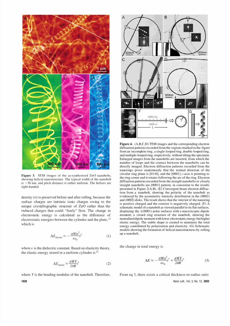
In addition to the significant portion of nanorings observed
in Figure 1, the most striking feature of the sample is the
formation of helical structures by rolling up single crystalline
nanobelts (Figure 3).25 The helical nanostructure has a
uniform shape with radii of ∼500-800 nm and evenly
distributed pitches. A nearly perfect circular arc is formed
by a single nanobelt (Figure 4A). Electron diffraction
indicates that the direction of the radius toward the center
of the ring is always [0001] along the entire perimeter
without significant twisting, and the circular plane of the
nanoring is [011h0]. A full circular ring formed by a closed
nanobelt shows a consistent orientation (Figure 4B); the
orientation of the straight or close-to-straight nanobelts is
along [0001], in consistent to the result from Figure 2A. The
orientation relationship presented in Figure 4A is preserved
Figure 1. SEM images of the as-synthesized ZnO nanobelts, showing nanobelts of sizes 20-60 nm in widths and a large fraction of nanorings and helical nanostructures.
1626 Nano Lett., Vol. 3, No. 12, 2003

8/3/2019 Xiang Yang Kong and Zhong Lin Wang- Spontaneous Polarization-Induced Nanohelixes, Nanosprings, and Nanorings …
http://slidepdf.com/reader/full/xiang-yang-kong-and-zhong-lin-wang-spontaneous-polarization-induced-nanohelixes 3/7
for nanorings formed by double-looped (Figure 4C) and
multiple-looped (Figure 4D) rolling of a nanobelt. The
orientation of the two wider nanobelts across the nanoring
in Figure 4C is [0001]. The enlarged images from the double-
looped ring in Figure 4C clearly indicate that the two loops
of the nanobelt are in physical contact, and there is even a
small gap (∼1-2 nm, see the insets in Figure 4C) between
them, suggesting that the interaction between the loops is
weak and there is no chemical bonding. Overlap among the
loops is possible for multiple-looped ring (see the inset in
Figure 4D).
The (0001) plane can be terminated with Zn [(0001)-Zn]
or oxygen [(0001h)-O], resulting in positively and negatively
charged top and bottom surfaces, respectively. Convergent
beam electron diffraction28 has been applied to determine
the polarity (Figure 4E), and the result indicates that the
interior surface of the ring is (0001)-Zn and the exterior
surface is (0001h)-O.29 Physically, if the surface charges are
uncompensated during the growth,30 the net dipole moment
tends to diverge and the electrostatic energy increases. For
a thin nanobelt laying on a substrate, the spontaneous
polarization induces electrostatic energy due to the dipole
moment, but rolling up to form a circular ring would
minimize or neutralize the overall dipole moment, reducing
the electrostatic energy. On the other hand, bending of the
nanobelt produces elastic energy. The stable shape of the
nanobelt is determined by the minimization of the total
energy contributed by spontaneous polarization and elasticity.
An analytical estimation of the total energy is given below.
A nanobelt with spontaneous polarization and charge on the
top and bottom surfaces can be approximated to be a
capacitor. For simplicity, we propose a model in which a
flat planar capacitor (length L, width W , and thickness t ) is
rolled up to form a cylindrical capacitor (inner radius R1,
outer radius R2, and mean radius R ) ( R1 + R2)/2), as shown
in Figure 4F. If the thickness of the nanobelt is much smaller
than the mean radius of the cylinder (t , R, and L ) 2π R)
(typically t ∼ 10 nm, R ∼ 500 nm), the surface charge
Figure 2. Controlled growth of (0001) polar-surface-dominated ZnO nanobelts. (A) Low-magnification TEM images and the correspondingelectron diffraction patterns recorded from the areas as indicated by a sequence number from an TEM grid without tilting, showing theirunanimous [0001] orientation on a flat carbon substrate. (B) TEM image and the corresponding electron diffraction pattern, showing thatthe nanobelt grows along [21h1h0] (a-axis), with ((0001) top and bottom surfaces, and ((011h0) side surfaces. (C) [0001] high-resolutionTEM image recorded from the center of the nanobelt given in (B), showing its dislocation-free volume. The inset is the projected modelof the wurtzite ZnO along [0001]; the positions of the Zn atoms are in correspondence to the white dots observed in the image. (D) [0001]
profile high-resolution TEM image recorded from the edge of the nanobelt given in (B), showing the flatness of the surface. (E) Lowmagnification TEM image and the corresponding electron diffraction patterns recorded from the circled regions, displaying the geometryof the nanobelt. The difference between the two electron diffraction patterns is due to the bending in the local regions. The contrast observedin the image is the bending contour in electron imaging produced by the deformation of atomic planes. (F) TEM image showing the helicaltwist of a nanobelt. The dark contrast at the top is due to the local strain. (G) Structure model of the ZnO nanobelt.
Nano Lett., Vol. 3, No. 12, 2003 1627
8/3/2019 Xiang Yang Kong and Zhong Lin Wang- Spontaneous Polarization-Induced Nanohelixes, Nanosprings, and Nanorings …
http://slidepdf.com/reader/full/xiang-yang-kong-and-zhong-lin-wang-spontaneous-polarization-induced-nanohelixes 4/7
density (σ ) is preserved before and after rolling, because the
surface charges are intrinsic ionic charges owing to the
unique crystallographic structure of ZnO rather than the
induced charges that could “freely” flow. The change in
electrostatic energy is calculated as the difference of
electrostatic energies between the cylinder and the plate,31
which is
where is the dielectric constant. Based on elasticity theory,
the elastic energy stored in a uniform cylinder is32
where Y is the bending modulus of the nanobelt. Therefore,
the change in total energy is
From eq 3, there exists a critical thickness-to-radius ratio
Figure 3. SEM images of the as-synthesized ZnO nanobelts,showing helical nanostructure. The typical width of the nanobeltis ∼30 nm, and pitch distance is rather uniform. The helixes areright-handed.
∆ E electro ≈ -π W σ
2
0
t 2
(1)
∆ E elastic ≈π WY
24 Rt
3(2)
Figure 4. (A,B,C,D) TEM images and the corresponding electrondiffraction patterns recorded from the regions marked in the figurefrom an incomplete ring, a single-looped ring, double-looped ring,and multiple-looped ring, respectively, without tilting the specimen.Enlarged images from the nanobelts are inserted, from which thenumber of loops and the contact between the nanobelts can bedirectly imaged. Electron diffraction patterns recorded from the
nanorings prove unanimously that the normal direction of thecircular ring plane is [011h0], and the [0001] c-axis is pointing tothe ring center and it rotates following the arc of the ring. Electrondiffraction patterns recorded from the straight nanobelts or closelystraight nanobelts are [0001] pattern, in consistent to the resultspresented in Figure 2(A,B). (E) Convergent beam electron diffrac-tion from a nanobelt, showing the polarity of the nanobelt asevidenced by the asymmetric intensity distribution in the (0002)and (0002h) disks. The result shows that the interior of the nanoringis positive charged and the exterior is negatively charged. (F) Aschematic model of a nanobelt as viewed parallel to its flat surfaces,displaying the ((0001) polar surfaces with a macroscopic dipolemoment; a closed ring structure of the nanobelt, showing theneutralized dipole moment with lower electrostatic energy but higherelastic energy. The stable shape is created to minimize the totalenergy contributed by polarization and elasticity. (G) Schematicmodels showing the formation of helical nanostructures by rollingup a nanobelt.
∆ E ≈ -π W σ
2
0
t 2
+π WY
24 Rt
3(3)
1628 Nano Lett., Vol. 3, No. 12, 2003
8/3/2019 Xiang Yang Kong and Zhong Lin Wang- Spontaneous Polarization-Induced Nanohelixes, Nanosprings, and Nanorings …
http://slidepdf.com/reader/full/xiang-yang-kong-and-zhong-lin-wang-spontaneous-polarization-induced-nanohelixes 5/7
(t / R)*, at which ∆ E ) 0,
where ∆ E < 0 if t / R < R, and ∆ E > 0 if t / R > R. The
bending modulus for free-standing nanobelts has been
measured by the mechanical resonance22 and nanoindenta-
tion33 techniques to be Y ) 50 ( 5 GPa, ) 4.6,34 and
surface charge density |σ | ) 0.057 C/m2 based on the first
principle calculation.24,30. Equation 4 gives R ) (3.8 ( 0.2)
× 10-2. Measurements from Figures 4A, B, and C give t / R
) (2.0 ( 0.1) × 10-2, (3.1 ( 0.1) × 10-2, and (2.8 ( 0.1)
× 10-2, respectively, all of which are smaller than the R
value from eq 4; thus, the nanoring structure is energetically
favorable. For a nanoring of typical radius of R ) 400 nm
as observed in Figure 1, eq 4 gives t * ≈ 15 nm. Therefore,
if the thickness of the nanobelt is smaller than 15 nm, the
total energy ∆ E drops after forming a ring, suggesting that
the ring configuration may be the preferred shape; while for
thicker nanobelts, the straight configuration is the stable
shape. The formation of the helical structure as shown in
Figure 3 is the simultaneous rolling of the nanobelt while it
continues to grow along the a-axis (Figure 4G).
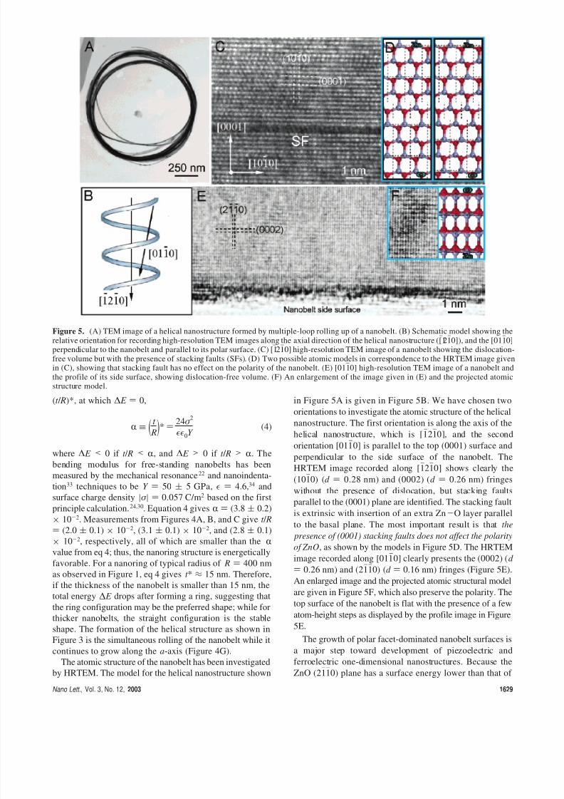
The atomic structure of the nanobelt has been investigated
by HRTEM. The model for the helical nanostructure shown
in Figure 5A is given in Figure 5B. We have chosen two
orientations to investigate the atomic structure of the helical
nanostructure. The first orientation is along the axis of the
helical nanostructure, which is [1h21h0], and the second
orientation [011h0] is parallel to the top (0001) surface and
perpendicular to the side surface of the nanobelt. The
HRTEM image recorded along [1h21h0] shows clearly the
(101h0) (d ) 0.28 nm) and (0002) (d ) 0.26 nm) fringes
without the presence of dislocation, but stacking faults
parallel to the (0001) plane are identified. The stacking fault
is extrinsic with insertion of an extra Zn-O layer parallel
to the basal plane. The most important result is that the
presence of (0001) stacking faults does not affect the polarity
of ZnO, as shown by the models in Figure 5D. The HRTEM
image recorded along [011h0] clearly presents the (0002) (d ) 0.26 nm) and (21h1h0) (d ) 0.16 nm) fringes (Figure 5E).
An enlarged image and the projected atomic structural model
are given in Figure 5F, which also preserve the polarity. The
top surface of the nanobelt is flat with the presence of a few
atom-height steps as displayed by the profile image in Figure
5E.
The growth of polar facet-dominated nanobelt surfaces is
a major step toward development of piezoelectric and
ferroelectric one-dimensional nanostructures. Because the
ZnO (21h1h0) plane has a surface energy lower than that of
Figure 5. (A) TEM image of a helical nanostructure formed by multiple-loop rolling up of a nanobelt. (B) Schematic model showing therelative orientation for recording high-resolution TEM images along the axial direction of the helical nanostructure ([1h21h0]), and the [011h0]perpendicular to the nanobelt and parallel to its polar surface. (C) [1h21h0] high-resolution TEM image of a nanobelt showing the dislocation-free volume but with the presence of stacking faults (SFs). (D) Two possible atomic models in correspondence to the HRTEM image givenin (C), showing that stacking fault has no effect on the polarity of the nanobelt. (E) [011h0] high-resolution TEM image of a nanobelt andthe profile of its side surface, showing dislocation-free volume. (F) An enlargement of the image given in (E) and the projected atomicstructure model.
R ≡ ( t R)* ) 24σ 2
0Y (4)
Nano Lett., Vol. 3, No. 12, 2003 1629
8/3/2019 Xiang Yang Kong and Zhong Lin Wang- Spontaneous Polarization-Induced Nanohelixes, Nanosprings, and Nanorings …
http://slidepdf.com/reader/full/xiang-yang-kong-and-zhong-lin-wang-spontaneous-polarization-induced-nanohelixes 6/7
either (0001) or (011h0), a fast growth along [21h1h0] (a-axis)
to form a nanobelt structure may be unfavorable from the
energy point of view. But the success of controlled growth
of free-standing (0001) polar-surface-dominated nanobelts
along the a-axis demonstrates the experimental feasibility
of overcoming the energy barrier through growth kinetics,
thus providing a feasible approach for growing structurally
controlled nanobelts of technological importance.
Helical structure is the most fundamental structural con-
figuration for DNA and many biological proteins, which isdue to van der Waals force and hydrogen bonding. For one-
dimensional nanostructures, nanocoils and nanorings have
been observed for carbon nanotubes35-37 and SiC,38 the
former are created due to a periodic arrangement of the paired
pentagon and heptagon carbon rings in the hexagonal carbon
network,39 and the latter are due to stacking faults and twins.
These helical structures are produced by the presence of point
or planar defects (twins and stacking faults). The striking
new feature of the helical nanostructures for single crystalline
ZnO nanobelt reported here is that they are the spontaneous
polarization induced structures.40 The nanobelts and helical
nanostructures are an ideal system for understanding piezo-
electricity and polarization-induced ferroelectricity at nanos-cale. Quantitative analysis about the elastic energy involved
in the formation of helical structure could provide an
experimental measurement on the electrostatic energy in-
duced by spontaneous polarization, leading to a possible
technique for measuring the dipole moment and surface
charge distribution in nanobelt structures. The different polar
surfaces could be used as selective catalysts. The piezoelec-
tric and ferroelectric nanobelt structures may open up many
research possibilities and applications at the nanoscale, such
as nanoinductors, nanospring-based transducers and actuators,
and tunable functional components for MEMS and NEMS.
The tunable pitch distance in the helical nanosprings could
be used for separating DNA double helix chains and tailoring
DNA structures via electromechanical coupling.41
Note Added after ASAP Posting. This article was posted
ASAP on 8/6/2003. Changes have been made in the Abstract,
the caption to Figure 3, and Figure 4. The correct version
was posted on 8/18/2003.
References
(1) Minne, S. C.; Manalis, S. R.; Quate, C. F. Appl. Phys. Lett. 1995,67 , 3918.
(2) See the special issue on transparent conducting oxides, MRS Bulletin,August issue, 2000.
(3) Gorla, C. R.; Emanetoglu, N. W.; Liang, S.; Mayo, W. E.; Lu, Y.;
Wraback, M.; Shen, H. J. Appl. Phys. 1999, 85, 2595.(4) Dulub, O.; Boatner, L. A.; Diebold, U. Surf. Sci. 2002, 519, 201.(5) Meyer, B.; Marx, D. Phys. ReV. B 2003, 67 , 035403.(6) Tasker, P. W. J. Phys. C: Solid State Phys. 1979, 12, 4977.(7) Dulub, O.; Diebold, U.; Kresse, G. Phys. ReV. Lett . 2003, 90, 016102-
1.(8) Wander, A.; Schedin, F.; Steadman, P.; Norris, A.; McGrath, R.;
Turner, T. S.; Thornton, G.; Harrison, N. M. Phys. ReV. Lett. 2001,86 , 3811.
(9) Staemmler, V.; Fink, K.; Meyer, B.; Marx, D.; Kunat, M.; Gil, G.S.; Burghaus, U.; Woll, Ch. Phys. ReV. Lett. 2003, 90, 106102-1.
(10) Cui, Y.; Lieber, C. M. Science 2001, 291, 851.(11) Huang, Y.; Duan, X. F.; Cui, Y.; Lauhon, L. J.; Kim, K. H.; Lieber,
C. M. Science 2001, 294, 1313.(12) Collins, P. C.; Arnold, M. S.; Avouris, Ph. Science 2001, 292, 706.
(13) Bachtold, A.; Hadley, P.; Nakanishi, T.; Dekker, C. Science 2001,294, 1317.
(14) Ma, D. D. D.; Lee, C. S.; Au, F. C. K.; Tong, S. Y.; Lee, S. T.Science 2003, 299, 1874.
(15) Duan, X. F.; Huang, Y.; Agarwal, R.; Lieber, C. M. Nature 2003,421, 241.
(16) Wang, Z. L., Ed.; Nanowires and Nanobelts, Vol. I: Metals and
Semiconductor Nanowires; Vol. II: Nanowires and Nanobelts of Functional Materials; Kluwer Academic Publisher: New York, 2003.
(17) Huang, M. H.; Mao, S.; Feick, H.; Yan, H.; Wu, Y.; Kind, H.; Weber,E.; Russo, R.; Yang, P. Science 2001, 292, 1897.
(18) Pan, Z. W.; Dai, Z. R.; Wang, Z. L. Science 2001, 291, 1947.
(19) Arnold, M.; Avouris, Ph.; Pan, Z. W.; Wang, Z. L. J. Phys. Chem. B 2002, 107 , 659.
(20) Comini, E.; Faglia, G.; Sberveglieri, G.; Pan, Z. W.; Wang, Z. L. Appl. Phys. Lett . 2002, 81, 1869.
(21) Hughes, W. L.; Wang, Z. L. Appl. Phys. Lett . 2003, 82, 2886.(22) Bai, X. D.; Wang, E. G.; Gao, P. X.; Wang, Z. L. Appl. Phys. Lett .
2003, 82, 4806.(23) Corso, A. D.; Posternak, M.; Resta, R.; Baldereschi, A. Phys. ReV.
B 1994, 50, 10715.(24) Bernardini, F.; Fiorentini, V.; Vanderbilt, D. Phys. ReV. B 1997, 56 ,
10024. The theoretically calculated piezoelectric coefficients for ZnOare: 33 ) 0.89, 31 ) -0.51 C/m2. The experimentally measured33 ) 1.0-1.2 C/m2.
(25) Wang, Z. L.; Kong, X. Y. Patent pending, Georgia Tech, 2003.(26) Kohl, D.; Henzler, M.; Heiland, G. Surf. Sci. 1974, 41, 403.(27) The as-synthesized samples were characterized by field emission
source scanning electron microscopy (SEM) (LEO 1530 FEG at 5
kV), high-resolution transmission electron microscopy (HRTEM)(Hitachi HF-2000 FEG at 200 kV and JEOL 4000EX at 400 kV).
(28) Vigue, F.; Vennegues, P.; Vezian, S.; Laugt, M.; Faurie, J.-P. Appl.Phys. Lett . 2001, 79, 194.
(29) The polarity of ZnO results in asymmetric intensity distribution inthe (0002) and (0002h) diffraction disks. The polarity was determinedby comparing the experimentally observed convergent beam electrondiffraction pattern with the theoretically calculated diffraction pattern.Details of the calculation can be found in Spence, J. C. H.; Zuo, J.M. Electron Microdiffraction; Plenum Press: New York, 1992.
(30) The local deposition temperature is ∼400-500 °C, which is highenough to prevent physical adsorption of molecules on the surfaceduring the growth. Thus, the ionic charges on the surface are likelyuncompensated and are electrostatically effective for producing thehelical structure.
(31) The calculation was made based on following approximations: [1]the thickness of the nanobelt is much smaller than the radius of the
nanoring (t , R); [2] the width (W ) of the nanobelt is significantlylarger than its thickness, so that the edge effect is small. However,it is the difference between the electrostatic energy before and afterrolling into a cylinder that matters to the final result; if the edgeeffect before and after rolling is preserved, the edge effect, if any, isalmost canceled out in the final equation. [3] The surface chargesare due to the unique crystallographic structure of ZnO, and theyare bound to the atoms, thus, the surface charge density is preservedafter rolling into a cylinder. Therefore, the total charge on the innersurface of the cylinder is Q ) 2π ( R - t /2)W σ . The change inelectrostatic energy is
∆ E electro )π W σ
2 R
2
0[(1 - β)
2ln(
1 + β
1 - β) - 2 β] ≈ -π W σ
2
0
t 2
(for t , R)where β ≡ t /2 R.
(32) Because the thickness of the nanobelt is very small and the ring radius
is large, the radial stress across the nanobelt is negligible becausethe two sides are free surfaces without external force. The strain alongthe z-direction (the axis of the cylinder) is also zero because there isno twisting. The only strain is along the φ-direction. The elasticenergy is the volume integration of the φ-direction strain energy.The bending modulus used for the calculation was based on theexperimentally measured value for ZnO nanobelts with inclusion of geometrical factor.
(33) Mao, S.; Zhao, M.; Wang, Z. L. Appl. Phys. Lett ., submitted.(34) Bernardini, F.; Fiorentini, V. Phys. ReV. B 1998, 58, 15292.(35) Amelinckx, S.; Zhang, X. B.; Bernaerts, D.; Zhang, X. F.; Ivanov,
V.; Nagy, J. B. Science 1994, 265, 635.(36) Martel, R.; Shea, H. R.; Avouris, Ph. Nature 1999, 398, 299.(37) Sano, M.; Kamino, A.; Okamura, J.; Shinkai, S. Science 2001, 293,
1299.
1630 Nano Lett., Vol. 3, No. 12, 2003

8/3/2019 Xiang Yang Kong and Zhong Lin Wang- Spontaneous Polarization-Induced Nanohelixes, Nanosprings, and Nanorings …
http://slidepdf.com/reader/full/xiang-yang-kong-and-zhong-lin-wang-spontaneous-polarization-induced-nanohelixes 7/7
(38) Zhang, H.-F.; Wang, C.-M.; Wang, L.-S. Nano Lett . 2002, 2, 941.(39) Gao, R. P.; Wang, Z. L.; Fan, S. S. J. Phys. Chem. B 2000, 104,
1227.(40) In-situ heating of the helical nanostructure has been carried out in
TEM under vacuum of 10-8 Torr. Heating the specimen to 400 °Cgenerated a high concentration of oxygen vacancies based ourprevious study in ref. 19, but no visible change in the shape of the
helical nanostructure was found, suggesting that the role played by
point defects in the formation of helical structure is undetectable.
(41) Thanks the support from NSF and NASA URETI. Thanks to Profs.
Min Zhou and Ashok Saxena for discussion.
NL034463P
Nano Lett., Vol. 3, No. 12, 2003 1631