self-assembled nanorings and stressor quantum...
TRANSCRIPT

Espoo, Finland 2006
SELF-ASSEMBLED NANORINGS AND
STRESSOR QUANTUM DOTS
Doctoral Dissertation
Juha Riikonen
Teknillinen korkeakoulu
Sähkö- ja tietoliikennetekniikan osasto
Optoelektroniikan laboratorio
Dissertation for the degree of Doctor of Science in Technology to be presented with due permission of
for public examination and debate inAuditorium
AS1 at (Espoo,Finland) on the 2nd of June,2006,at 12 noon.
the
Department of Electrical and Communications Engineering
Helsinki University ofTechnology
Helsinki University of Technology
Department of Electrical and Communications Engineering
Optoelectronics Laboratory

Distribution:
Helsinki University of Technology
Department of Electrical and Communications Engineering
Optoelectronics Laboratory
P.O. Box 3500
FIN-02015 TKK
FINLAND
Tel: +358 9 4511
Fax: +358 9 451 3128
E-mail: [email protected]
© 2006 Juha Riikonen
ISBN 951-22-8181-3 (printed version)
ISBN 951-22-8182-1 (electronic version)
URL: http://lib.tkk.fi/Diss/2006/isbn9512281821/
Otamedia Oy
Espoo 2006
ABHELSINKI UNIVERSITY OF TECHNOLOGYP. O. BOX 1000, FI-02015 TKK
http://www.tkk.fi
ABSTRACT OF DOCTORAL DISSERTATION
Author Juha Riikonen
Name of the dissertation
Date of manuscript 23rd January 2006 Date of the dissertation 2nd June 2006
Article dissertation (overview + original articles) Number of pages 56+62
Department
Laboratory
Field of research
Opponent
Supervisor
Abstract
Keywords MOVPE, epitaxy, nanotechnology, self-assembled, compound semiconductor,quantum dot, nanoring, quantum ring, passivation
ISBN (printed) 951-22-8181-3 ISBN (electronic) 951-22-8182-1
Publisher TKK Optoelectronics Laboratory
The dissertation can be read at http://lib.tkk.fi/Diss/2006/isbn9512281821/
Self-assembled nanorings and stressor quantum dots
Department of Electrical and Communications Engineering
Optoelectronics laboratory
Nanotechnology
Prof. Srinivasan Anand
Prof. Harri Lipsanen
In this thesis, the main focus is in the fabrication and characterization of self-assembled III-V compound semiconductor nanostructures. The samples were fabricated by metalorganicvapor phase epitaxy (MOVPE). Atomic force microscopy (AFM) and photoluminescence (PL)measurements were used to examine surface morphology and optical characteristics of thesamples, respectively.
Quantum dot (QD) heterostructures are typically realized by embedding self-assembled islandsin a matrix of another semiconductor material with a higher band gap. In this work, however,islands were used as stressors on top of a near-surface quantum well (QW) to induce three-dimensional potential enclosures into the QW. These QD structures are known as strain-induced QDs (SIQDs) or stressor QDs. Firstly, a new material system utilizing InAs stressorislands to create strain-induced InGaAs(P)/InP QDs was demonstrated. Up to four PL peaksfrom the QD ground and excited states were clearly resolved in the spectra. The island ensemblewas optimized using a growth temperature ramp-down during the InAs island deposition. Theluminescence wavelength was tuned by varying the QW composition. On the other hand, theQD confinement was modified by altering the height of the stressor islands or by varying thedistance of the QW from the surface.
Secondly, transformation of self-assembled InAs islands into volcano-like nanorings was investi-gated. In the method introduced in this thesis, contrary to previous techniques utilizing partialcapping of islands, only phosphorus annealing was applied. It is assumed that the materialredistribution, i.e., the island-to-ring transformation, is caused by the exchange of As atomsto P atoms along with the strain-driven migration of In atoms outwards from the island.
Thirdly, surface passivation of GaAs by an in situ grown epitaxial ultrathin GaN layer wasstudied. Near-surface InGaAs/GaAs QWs were used as low-dimensional test structures, onwhich the passivation was applied. PL measurements were used to assess the effect of thepassivation. Significant enhancement of the PL intensity shows that the growth of an ultrathinGaN layers is an efficient method in the passivation of GaAs surfaces.

ABTEKNILLINEN KORKEAKOULU
PL 1000, 02015 TKK
http://www.tkk.fi
VÄITÖSKIRJAN TIIVISTELMÄ
Tekijä Juha Riikonen
Väitöskirjan nimi
Käsikirjoituksen jättämispäivämäärä 23.1.2006 Väitöstilaisuuden ajankohta 2.6.2006
Yhdistelmäväitöskirja (yhteenveto + erillisartikkelit) Sivumäärä 56+62
Osasto
Laboratorio
Tutkimusala
Vastaväittäjä
Työn valvoja
Tiivistelmä
Avainsanat MOVPE, epitaksia, nanoteknologia, itsejärjestäytyvä, yhdistepuolijohde,kvanttipiste, kvanttirengas, nanorengas, passivointi
ISBN (painettu) 951-22-8181-3 ISBN (elektroninen) 951-22-8182-1
Julkaisija TKK Optoelectroniikan laboratorio
Luettavissa verkossa osoitteessa http://lib.tkk.fi/Diss/2006/isbn9512281821/
Itseorganisoituvat nanorenkaat ja jännityksen indusoimat kvanttipisteet
Sähkö- ja tietoliikennetekniikan osasto
Optoelektroniikan laboratorio
Nanotekniikka
Prof. Srinivasan Anand
Prof. Harri Lipsanen
Tässä väitöstyössä valmistettiin ja tutkittiin itsejärjestyviä yhdistepuolijohteiden nanoraken-teita. Näytteet valmistettiin metallo-orgaanisella kaasufaasiepitaktisella (engl. metalorganicvapor phase epitaxy, MOVPE) menetelmällä. Atomivoimamikroskopiaa (engl. atomic forcemicroscopy, AFM) käytettiin pinnan morfologian tutkimiseen. Optisia ominaisuuksia tutkittiinfotoluminesenssimittauksilla (engl. photoluminescence, PL).
Kvanttipisteitä on tyypillisesti valmistettu peittämällä itsejärjestyneitä puolijohdesaarekkeitatoisella puolijohteella, jolla on saarekemateriaalia suurempi energia-aukko. Tässä työssä kvant-tipisteitä kuitenkin valmistettiin pinnan läheisyydessä olevaan kvanttikaivoon saarekkeidenindusoiman jännityksen avulla (nk. jännityskvanttipisteet). Aluksi toteutettiin jännityskvant-tipisteiden valmistamiseen soveltuva uusi materiaalisysteemi, jossa käytettiin InGaAs(P)/InP-kvanttikaivoa sekä InAs-saarekkeita. PL-spektrissä havaittiin selkeästi neljän jännityskvant-tipistetilan maksimit. Saarekekokonaisuutta optimoitiin laskemalla lämpötilaa saarekekasvunaikana. Jännityskvanttipisteiden luminesenssiaallonpituutta säädettiin kvanttikaivon koostu-musta muuttamalla. Lisäksi kvanttipisteiden ominaisuuksia muutettiin mm. valmistamalla erikokoisia saarekkeita sekä vaihtelemalla kvanttikaivon etäisyyttä pinnasta.
Seuraavaksi työssä tutkittiin itsejärjestyvien InAs-saarekkeiden muodon muuttamistananorenkaiksi. Aikaisemmissa tutkimuksissa muodonmuutoksessa hyödynnettiin saarekkeidenosittaista peittämistä. Tässä työssä muodonmuutos saatiin aikaan käyttämällä ainoastaanfosforilämpökäsittelyä. Muodonmuutoksen oletetaan aiheutuvan aluksi tapahtuvasta arseeni-atomien vaihtumisesta fosforiatomeiksi sekä tätä seuraavasta indiumatomien uudelleen ryhmit-tymisestä energeettisesti edullisempiin paikkoihin.
Lopuksi tutkittiin GaAs-pinnan passivointia ohuen epitaktisen GaN-kerroksen avulla. Pas-sivoinnin vaikutusta arvioitiin mittaamalla PL-spektrejä näytteistä, joissa InGaAs/GaAs-kvanttikaivo on pinnan läheisyydessä. Passivointikerroksen aikaansaaman PL-intensiteetinkasvun perusteella pääteltiin, että epitaktisesti valmistettu GaN-kerros on tehokas tapa pas-sivoida GaAs-pinta.

Preface
The work presented in this thesis has been carried out at the OptoelectronicsLaboratory of Helsinki University of Technology during 2000 – 2005. I wantto express my gratitude to Professor Turkka Tuomi and Professor HarriLipsanen for giving me the opportunity to work at the laboratory and fortheir continuous support during this time.
I like to thank Docent Markku Sopanen for guidance and advice. I amdeeply indebted to him for his help. I would also like to thank my col-laborator Doctor Jaakko Sormunen. Our cooperation has been pleasantand, moreover, productive. I thank Marco Mattila and Hannu Koskenvaarafor their valuable assistance and fruitful conversations on the way. All thepersonnel in Optoelectronics laboratory I want to thank for the enjoyableatmosphere.
The financial support of the Graduate School of Electronics Manufacturingis gratefully acknowledged.
I thank my parents for encouragement and support throughout the journey,and sisters Jaana and Johanna for putting up with me all these years.Finally, I want to thank my loving wife Tanja and delightful daughter Enni— You are my inspiration.
“It is quite probable that other new physical principles will also be utilized topractical ends as the art develops.”
— WILLIAM SHOCKLEY in his Nobel Lecture, December 11, 1956.
Espoo, May 2006
Juha Riikonen
vii

Table of Contents
Preface . . . . . . . . . . . . . . . . . . . . . . . . . . . . . . . . vii
Table of Contents . . . . . . . . . . . . . . . . . . . . . . . . . . . viii
List of Publications . . . . . . . . . . . . . . . . . . . . . . . . . . x
Author’s contribution . . . . . . . . . . . . . . . . . . . . . . . . xi
1 Introduction 1
2 Experimental methods 4
2.1 Metalorganic vapor phase epitaxy . . . . . . . . . . . . . . . 4
2.2 Atomic force microscopy . . . . . . . . . . . . . . . . . . . . 6
2.3 Optical spectroscopy . . . . . . . . . . . . . . . . . . . . . . 7
3 III-V semiconductor nanostructures: an introduction 9
3.1 Fabrication . . . . . . . . . . . . . . . . . . . . . . . . . . . 9
3.2 Strain-induced quantum dots by self-assembled growth . . . 11
3.3 Self-assembled nanorings . . . . . . . . . . . . . . . . . . . . 15
4 Experimental results and discussion 18
4.1 Strain-induced InGaAs(P)/InP quantum dots . . . . . . . . 18
4.1.1 Demonstration of self-assembled InAs stressors islands 18
viii
4.1.2 Modification and tunability . . . . . . . . . . . . . . 20
4.1.3 Time-resolved optical properties . . . . . . . . . . . 25
4.2 InAs nanorings on InP . . . . . . . . . . . . . . . . . . . . . 29
4.2.1 Fabrication of self-assembled nanorings . . . . . . . . 29
4.2.2 Island-to-ring evolution . . . . . . . . . . . . . . . . 31
4.3 GaN passivation of GaAs surface . . . . . . . . . . . . . . . 33
5 Summary 38
References 40
ix
List of Publications
This thesis consists of an overview and of the following publications:
I J. Riikonen, J. Sormunen, M. Mattila, M. Sopanen, and H. Lipsanen,InGaAs/InP quantum dots induced by self-organized InAs stressor-islands, Japanese Journal of Applied Physics 44, L518–L520 (2005).
II J. Sormunen, J. Riikonen, M. Mattila, M. Sopanen, and H. Lipsanen,Modified self-assembly of InAs islands acting as stressors for strain-induced InGaAs(P)/InP quantum dots, Nanotechnology 16, 1630–1635 (2005).
III J. Riikonen, J. Sormunen, H. Koskenvaara, M. Mattila, M. Sopa-nen, and H. Lipsanen, Highly tunable emission from strain-inducedInGaAsP/InP quantum dots, Japanese Journal of Applied Physics44, L976–L978 (2005).
IV H. Koskenvaara, J. Riikonen, J. Sormunen, M. Sopanen, and H. Lip-sanen, Carrier dynamics in strain-induced InGaAsP/InP quantumdots, accepted for publication in Physica E.
V J. Riikonen, J. Sormunen, H. Koskenvaara, M. Mattila, A. Aierken,T. Hakkarainen, M. Sopanen, and H. Lipsanen, Effect of surfacestates on carrier dynamics in InGaAsP/InP stressor quantum dots,Nanotechnology 17, 2181–2186 (2006).
VI J. Sormunen, J. Riikonen, M. Mattila, J. Tiilikainen, M. Sopanen,and H. Lipsanen, Transformation of self-assembled InAs/InP quan-tum dots into quantum rings without capping, Nano Letters 5, 1541–1543 (2005).
VII J. Sormunen, J. Riikonen, T. Hakkarainen, M. Sopanen, and H. Lip-sanen, Evolution of self-assembled InAs/InP islands into quantumrings, Japanese Journal of Applied Physics 44, L1323–L1325 (2005).
VIII J. Sormunen, J. Riikonen, M. Sopanen, and H. Lipsanen,GaN/GaAs(100) superlattices grown by metalorganic vapor phaseepitaxy using dimethylhydrazine precursor, Journal of CrystalGrowth 270, 346–350 (2004).
IX J. Riikonen, J. Sormunen, H. Koskenvaara, M. Mattila, M. Sopanen,and H. Lipsanen, Passivation of GaAs surface by ultrathin epitaxialGaN layer, Journal of Crystal Growth 272, 621–626 (2004).
x

Author’s contribution
For all of the publications, the sample structures and experiments wereplanned by the author and the co-authors.
The author and J. Sormunen have fabricated the samples for publicationsI, II, III, IV, V, VIII, and IX. For publications VI and VII samples weregrown by J. Sormunen.
Photoluminescence measurements for publications I, II, III, VI, and IX wereperformed by the author. For publication V the studies were carried outby the author, A. Aierken, and H. Koskenvaara and for publication VII byJ. Sormunen.
The surface morphology for publication V was analyzed by the author. Forthe rest of the publications, analyses were conducted by J. Sormunen.
Strain calculations have been conducted by M. Mattila and rate equationanalyses have been carried out by H. Koskenvaara.
The author has written the manuscripts for publications I, III, V, and IXand has also participated in the interpretations of the results and revisionof the manuscripts for the publications II, IV, VI, VII, and VIII.
xi

1 Introduction
The usefulness of semiconductors was truly revealed upon the invention ofthe transistor. Since then, the semiconductor technology and its applica-tions have evolved tremendously. For example, the mobile phones with avideo call and live television were just a vague dream some years ago andwithout semiconductor technology there would be no Internet as we knowit today. Electronic circuit miniaturization and circuit integration alongsidewith the extraordinary properties of semiconductors have made all of thispossible.
Silicon is the standard material in electronics involving integrated circuits.However, silicon is not suitable for light emitting devices due to its fun-damental physical properties. Thus, III-V compound semiconductors arepredominantly used in optoelectronics for the fabrication of optically activedevices such as light emitting diodes (LEDs) and lasers. Laser diodes, e.g.,form the backbone of the Internet by enabling fiber optical telecommunica-tion.
In the evolutionary process of applications, advances in device design aretruly important, but the fabrication technology needs to reach a maturestate, as well. The ever-ongoing development of heteroepitaxial fabrica-tion techniques has enabled the realization of state-of-the-art compoundsemiconductor structures. With heteroepitaxy, two-dimensional layers orthin films can be used to fabricate a quantum well (QW) structure in or-der to confine charge carriers in one dimension (1D). On the other hand,to produce three-dimensional (3D) confinement, i.e., quantum dots (QDs),self-assembled semiconductor islands are typically embedded in a matrix ofanother semiconductor material with a higher band gap (so-called buriedQDs). These kinds of structures can be used as an optically active region,e.g., in lasers.
In the pursuit of new applications, nanotechnology has recently evoked moreinterest. This interdisciplinary field of science focuses on, as the name im-
1
2
plies, structures on the nanometer scale. Quantum mechanics play an essen-tial role in determining the novel characteristics of structures on this scale,e.g., carrier confinement in a QD results in an energy level quantization.In many cases, nanostructures are fabricated by exploiting the ability ofnature to self-organize or self-assemble atoms and molecules. This thesiscombines optoelectronics and nanotechnology, and mainly focuses on theepitaxial self-assembled islands and how they are exploited especially in thefabrication of QD structures.
Besides creating QDs by burying self-assembled islands, also strain-inducedQDs (SIQDs) or stressor QDs can be fabricated. SIQDs are realized bystraining a near-surface QW by self-assembled islands. The stressor islandson top of the structure induce confining enclosures, i.e., QDs, in the QW.Moreover, SIQDs present an intriguing structure in the pursuit of high op-tical quality QDs, because these QDs reside within a high quality QW awayfrom the sample surface. The main focus in this thesis is in the fabricationand investigation of SIQDs. In publication I, a novel SIQD material systemutilizing InGaAs/InP QW and InAs islands as stressors was demonstrated.In publications II and III, modification and tunability of InGaAs(P)/InPSIQDs were studied. Carrier dynamics of InGaAsP/InP SIQDs was inves-tigated in publications IV and V.
While fabricating buried QDs, self-assembled islands are capped by fullyovergrowing them. On the other hand, partial capping can be used totransform the morphology of the islands into volcano-like nanorings (NRs).These nanostructures present an interesting topic in nanotechnology dueto the potential offered by the unique topology. Moreover, investigationof the island-to-ring transformation helps to further refine the growth ofself-assembled islands especially when fabricating buried QDs. In publi-cations VI and VII, fabrication and characteristics of self-assembled InAsnanorings on InP were studied. Instead of employing the typical approachof partial capping, a new island-to-ring transformation process without cap-ping was demonstrated.
Disruption of the periodic semiconductor crystal lattice by the sample sur-face can lead to the formation of electrically active surface states, whichare usually detrimental to the optical and electrical characteristics, and es-pecially so in low-dimensional structures. Consequently, exploitation of anepitaxial ultrathin GaN layer in the passivation of a GaAs surface was alsostudied in this thesis. Growth of GaN on GaAs was based on the resultsin publication VIII and passivation by GaN was studied in publication IX.

3
Near-surface InGaAs/GaAs QWs were used as a low-dimensional test struc-tures in the passivation studies.
This overview has been organized as follows. The main experimental meth-ods used in this thesis are described in chapter 2. A short introduction toIII-V compound semiconductor nanostructures within the scope of this the-sis is given in chapter 3. The experimental results of this work are presentedin chapter 4. More specifically, section 4.1 summarizes the work on strain-induced InGaAs(P)/InP QDs. InAs nanorings are discussed in section 4.2.Section 4.3 presents results on the GaN passivation of a GaAs surface. Fi-nally, the main results of this thesis are summarized in chapter 5.

2 Experimental methods
The experimental techniques essential to this thesis are introduced in thischapter. The sample fabrication by metalorganic vapor phase epitaxy(MOVPE) is explained in section 2.1. Section 2.2 presents atomic forcemicroscopy (AFM) used to characterize the surface morphology of the sam-ples. Optical spectroscopy measurements are outlined in section 2.3.
2.1 Metalorganic vapor phase epitaxy
MOVPE is a method of chemical vapor deposition for the epitaxial growthof materials utilizing the pyrolysis of metalorganic compounds. In epitaxialgrowth, the crystalline structure of the substrate is reproduced or mimed tothe deposited layer. More specifically, it is called homoepitaxy if the sub-strate and the deposited material are the same. Term heteroepitaxy, on theother hand, is used when one material is grown on another (e.g. InGaAs onInP). The MOVPE process or apparatus is also referred to as organometallicvapor phase epitaxy (OMVPE), organometallic chemical vapor deposition(OMCVD), and metalorganic chemical vapor deposition (MOCVD). Theterm MOVPE is used throughout this thesis.
In general, chemical vapor deposition (CVD) results from chemical reac-tions of precursors in the vicinity of the substrate typically at temperaturesbetween 500 and 1100
◦
C. MOVPE is a specific CVD process, which utilizesmetalorganic compounds as precursors and it is especially suitable for thefabrication of semiconductor single crystals. MOVPE enables, e.g., the fab-rication of highly homogeneous layers, atomically flat surfaces, and sharpinterfaces in heteroepitaxy while controlling the composition precisely. Inorder to gain reproducibility, computers are typically used to control theMOVPE systems during the growth process.
4

5
The semiconductor structures studied in this thesis were fabricated by aMOVPE system manufactured by Thomas Swan Scientific Equipment Ltd.The main parts of the MOVPE: the gas system, reactor, and gas exhaust andcleaning are shown schematically in Fig. 2.1. The metalorganic precursorsare in steel containers known as bubblers. Carrier gas, in this case hydro-gen, is used to transport the metalorganic compounds. The concentration ofmetalorganics in the carrier gas is determined by the vapor pressure of theprecursor, which can be controlled by adjusting the precursor temperature.In order to provide a stable concentration of metalorganics, the bubblersare located in temperature controlled baths. Metalorganics used in thisthesis were trimethylgallium (TMGa), trimethylindium (TMIn), tertiary-butylphosphine (TBP), tertiarybutylarsine (TBAs), and dimethylhydrazine(DMHy).
lampthermo-couple
susceptor
substratereactor
TMIn, TBAs, TBP, ...
MFCs
...bubblers
baths
carrier gas
exhaust(to gas scrubber)
vent line
mixing manifolds
gas system
gas exhaust and cleaning
pyrolysisfurnace
H2
Figure 2.1. Schematic diagram of the MOVPE system.
The flow rate of the gas is controlled by mass flow controllers (MFCs)throughout the system. Mixing manifolds are used to direct the metalor-ganic compounds to the reactor whereas the vent line is used to flush thegas directly to the exhaust. For example, while growing an InP layer, TMInand TBP are lead to the reactor while the rest of the organometallics aredirected to the vent line, as indicated in Fig. 2.1. All the exhaust gasesfrom the reactor and the vent line are finally absorbed and oxidized in ascrubber.
The epitaxial growth takes place in the horizontal quartz-glass reactor wherethe substrate is placed on a graphite susceptor. The maximum size of thesubstrate is 2×2 cm2. The susceptor is heated by a halogen lamp, which islocated outside the reactor underneath the susceptor, as depicted in Fig. 2.1.

6
The temperature is measured by a thermocouple inside the susceptor. Itshould be noted that the gas flow cools the substrate. In a similar reac-tor, when the thermocouple reading is 650
◦
C the actual temperature atthe sample surface is approximately 50
◦
C lower [1]. All the temperaturesmentioned in this thesis are thermocouple readings.
The samples in this thesis were fabricated on semi-insulating InP(001) andGaAs(001) substrates at atmospheric pressure. Prior to the growth processthe substrates were annealed at 650–700
◦
C in the reactor to remove thenative oxide. The temperature in the growth process was typically between540 and 640
◦
C whereas the growth rate was around 0.3 nm/s. Detailedinformation about the growth procedures can be found in section 4 of thisoverview and in the publications of this thesis.
2.2 Atomic force microscopy
Atomic force microscopy was invented by Binning et al. in 1986 [2]. Theydescribed the atomic force microscope as a combination of the principlesof the scanning tunneling microscope (STM) and the stylus profilometer.As depicted in Fig. 2.2, the basic principle of the AFM is quite simple. Asharp tip, typically composed of silicon or silicon nitride, on a cantilever isbrought into a close proximity of the surface. At the same time, a laser beamis used to detect the deflection of the cantilever caused by an electrostaticforce between the tip and the sample. Feedback is used to keep the force,i.e., the distance, between the tip and the sample constant. This is doneby moving the sample or tip vertically using piezoelectric actuators. Inorder to scan a map of the surface features, similar actuators are used tomove the sample or tip in lateral directions. The AFM technique achievesa high magnification of the surface features in all three dimensions contraryto optical or electron microscopes (which provide a two-dimensional (2D)projection of the surface). Moreover, AFM is rather versatile since themeasurement can be carried out in ambient air and the samples do notneed any special preparation. It can be also used to measure conducting aswell as insulating samples.
The maximum scan area of the contact-mode NanoScope E AFM utilizedin this thesis is 13×13 µm2. Nominal radius of the non-conductive siliconnitride tips used is 10 nm. In detailed analysis, the finite curvature of the tipshould be taken into consideration, since the scanned image is a convolutionof the tip and the surface profile. In this thesis, AFM is mainly used to study

7
detector
sample
cantilever
laser beamfeedback
scanlinex, y, z
movementtip atoms
surface atomsforce
Figure 2.2. A schematic illustration of atomic force microscopy.
the areal density and the size of self-assembled InAs islands. Because thenumber of the islands in the maximum scan area is typically around 2000and the size of the islands needs not to be determined to extreme precision,these shortcomings do not play a significant role.
2.3 Optical spectroscopy
The optical properties of the samples investigated in this thesis were studiedby photoluminescence (PL) measurements. The term photoluminescence isused when light is utilized for excitation in order to gain luminescence froma substance. Electron–hole pairs created in photon absorption thermalizerapidly to the band edge and then the carriers move by diffusion and drift.In a semiconductor structure with a QW, for example, the carriers areeasily transported to the QW region. Before recombination, free carriers aremostly relaxed to the ground state of the QW. Information about the energylevel structure [publications I–IX] and the carrier dynamics [publications III,IV, V] of the samples can be gatherer by studying the emission spectra andthe temporal behavior of the PL, respectively.
In this thesis, the optical properties of the samples were studied by low-temperature (10 K) continuous-wave photoluminescence (cw-PL) and time-resolved photoluminescence. The setup used for the cw-PL is shown inFig. 2.3 (a). The samples were cooled in a closed-cycle helium cryostat. In

8
computer
pumplasermonochromator
photomultiplier
monochromator
detector
cryostat
lens
chopper
lens
lock-in amplifier
attenuator mirrorlaser beam
referencefrequency
lens
sample
computer
A/D converterlaser
filter
(a)
(b)cryostat lens
lens attenuator
mirrorlaser beam
lens
sample
amplifier
filter
beamsplitter
pulse laser
synchrodetector
time-correlatedphoton countingelectronics
Figure 2.3. Schematic diagram of (a) the continuous-wave PL and(b) time-resolved PL setup.
the cw-PL measurements a frequency-doubled Nd:YVO4 laser operating at532 nm was used for excitation. In publication IX, however, a 488 nm linefrom an argon-ion laser was used for optical excitation. The PL spectrawere recorded using a 0.5 m monochromator with a germanium detectorcooled to liquid nitrogen temperature while utilizing a lock-in amplifier.
The TRPL measurements were performed by exciting the samples with 150-fs pulses at 800 nm from a mode-locked Ti:sapphire laser with a repetitionrate of 76 MHz (Fig. 2.3 (b)). The laser used in cw-PL was used as a pump-laser for the Ti:sapphire laser. The PL transients at selected wavelengthswere detected by a Peltier-cooled microchannel plate photomultiplier andtime-correlated single photon counting electronics. The temporal resolutionof the system was approximately 30 ps.

3 III-V semiconductor
nanostructures: an introduction
This chapter gives a brief introduction to semiconductor nanostructures.Fabrication is outlined briefly in section 3.1. Strain-induced quantum dotsare introduced in section 3.2 whereas self-assembled nanorings are discussedin section 3.3.
3.1 Fabrication
Nanostructure is quite commonly defined in semiconductor physics as astructure with two or three dimensions in the nanometer scale. When themovement of the carrier is restricted sufficiently at least in one dimension,quantum confinement or quantization can be achieved. More specifically,the size of the confinement needs to be comparable to the Bohr excitonradius. As a rule of thumb, for typical III-V semiconductors the transitionto strong confinement occurs when the dimension is around 10 nm [3]. Ina quantum well structure, electrons and holes are confined in 1D. On theother hand, in quantum wires and quantum dots, the confinement potentialis in 2D and 3D, respectively. A quantum well is typically fabricated byembedding or sandwiching a thin layer of low band gap material in a highband gap material. Quantum dots, on the other hand, can be createdby burying 3D nanoscale structures in a matrix of another semiconductorhaving a larger band gap. Typical QD fabrication techniques are describedin the following section.
Basically, the different ways to create semiconductor nanostructures (andstructures in general) can be divided into two classes. Despite the differentapproach of these techniques, they are mainly considered as complemen-tary methods in device fabrication. One class of methods is called top-down
9

10
techniques. These methods are used to create structures by removing (orcarving) material and can, e.g., involve electron beam (e-beam) lithogra-phy and etching processes. Top-down techniques are especially suitable infabricating microstructures such as cantilevers for microelectromechanicalsystems (MEMS) or finalizing device structures of laser diodes. Anotherclass of methods is called bottom-up techniques. These methods utilizeself-assembled or self-organized growth in order to generate structural or-ganization of atoms. Self-assembled nanostructures can be fabricated, e.g.,by heteroepitaxy as has been done in this thesis.
(a) (b) (c)
Figure 3.1. The basic growth modes in heteroepitaxy are(a) Frank-van der Merwe, (b) Volmer-Weber, and (c) Stranski-Krastanow.
The three fundamentally different growth modes in heteroepitaxy are shownschematically in Fig. 3.1. The layer-by-layer growth, shown in (a), is calledthe Frank-van der Merwe growth mode [4]. This 2D layer growth can beused to fabricate two-dimensional layer structures, e.g., QWs. However, thepseudomorphic strain between the layers sets a limitation to the maximumthickness. Beyond this so-called critical thickness the strained layer relaxesby generating misfit dislocations.
In the Volmer-Weber growth [5], on the other hand, the deposited atomsform 3D islands directly on the surface, as depicted in Fig. 3.1 (b). TheStranski-Krastanow growth mode [6], shown in (c), is initiated by 2D layergrowth. It is typically referred to as wetting layer. However, as the criticalthickness (typically few monolayers, MLs) is achieved, island formation be-gins. An important aspect in the self-assembled Stranski-Krastanow (S-K)growth mode is that it can be used to fabricate non-dislocated, i.e., co-herently strained islands [7]. As a result, islands grown by the so-calledcoherent S-K growth can be used in optically active structures.

11
3.2 Strain-induced quantum dots by
self-assembled growth
The common way to fabricate QDs is to bury self-assembled islands in amatrix of another semiconductor having a larger band gap, shown schemat-ically in Fig. 3.2 (a). Alternatively, a QD can also be realized by using aQW structure as a starting point and introducing the lateral confinementby other means, shown in Figs. 3.2 (b) – (d).
(a) (b) (d)(c)
islands
substrate
QW
strained layer
stressor island
QD in QW
mesa stressorQW mesa
near-surface QWs
barrier
barrier
SIQDs
buried islands
Figure 3.2. QDs created utilizing (a) buried islands, (b) etchedQW mesa, (c) SIQD by strained mesa, and (d) SIQD by self-assembled stressor islands. The QD is formed (a) in the islandsthemselves and (b) – (d) in the near-surface QW.
Using the top-down approach, as depicted in (b), an etched mesa can beused to create lateral confinement in the planar QW structure [8, 9]. In thisstructure, however, the large etched surface with crystal defects created inthe etching process can be detrimental to the quantum efficiency of lightemission. A more sophisticated approach is to grow a pseudomorphic com-pressively strained layer on top of a near-surface QW structure [10]. Theetched mesa of the strained layer, called a stressor, creates local strain un-derneath the stressor, which effectively creates a strain-induced QD insidethe near-surface QW as depicted in (c). These were the first strain-inducedQDs reported. However, the critical thickness of the strained layer limits

12
the maximum strain. As a consequence, the achieved confinement is quiteweak. All in all, the top-down methods do not usually provide viable meansto create high quality QD structures.
As shown in Fig. 3.2 (d), self-assembled islands grown on top of the cappinglayer of the near-surface QW structure can also be utilized as stressors tocreate strain-induced QDs into a near-surface QW. With this method, firstdemonstrated by Sopanen et al. [11], the structure can be fabricated in situwith a single growth run requiring no additional processing steps. Whilefabricating QDs utilizing QW mesa or mesa stressor structures, e.g, by e-beam lithography, the lateral position of the QDs can be determined exactly.This cannot be done in self-assembled growth, and it is not even necessary intypical optoelectronic applications. More importantly, the size, shape, andareal density of the nanostructures can be varied in self-assembled growth.In the e-beam technique, the structures are patterned one by one whereasby self-assembled growth, islands with an areal density of around 109 cm−2
can be fabricated even on several wafers in one growth run. Moreover, thecoherent self-assembled islands induce larger strain on the QW underneath,which results in a deeper confinement potential. More specifically, as shownin Fig. 3.3 (a), the tensile strain reduces the band gap of the materialunderneath the stressor island. The local deformation creates a lateral (orin-plane) confinement potential for both electrons and holes. The verticalconfinement, on the other hand, is achieved by the high-quality interfacesof the QW. As a result, the SIQD is formed into a strain-modified region ofthe QW.
(a)
QD2
QW
QD1QD0
EV
EC
SIQD
stressor island
0.70 0.75 0.80
(b)
QD2QD1
QW
PL energy (eV)
QD0
Figure 3.3. (a) Schematic illustration of the in-plane confinementpotential and (b) a typical SIQD PL spectrum of the SIQD.

13
Fig. 3.3 (b) shows a typical SIQD PL spectrum [publication III]. The PLpeaks corresponding to QD ground state along with the first and secondexcited states are labeled with QD0, QD1 and QD2, respectively. To un-derstand the observed PL behavior, carrier relaxation and recombinationprocesses are briefly discussed based on the studies of InGaAs/GaAs SIQDs[12]. Carriers created by excitation are directed by the funnel-like poten-tial1 toward the SIQDs [13]. Then, the carriers relax either straight intothe SIQD or to the QW, from which they are mainly recombined radiativelyor captured into the SIQD (referred to as QD capture). The QD captureprocess is mediated by Coulomb scattering and longitudinal optical phononemission [14, 15]. Once captured into the SIQD, the holes and electronscan either experience relaxation to the lower energy states or recombineradiatively. Two mechanisms are reported to be responsible for the intra-band relaxation of the carriers: Coulomb scattering is shown to be effectivewhen the QW is highly populated [14] whereas an Auger-like mechanismhas been reported to mediate the relaxation in a low density case [16]. ThisAuger-like process involves the transition of an electron to a lower level inthe SIQD, while a hole is ejected into the QW.
A review of the SIQDs by Lipsanen et al. [12] says that “the most promi-nent feature in the optical properties of the stressor QDs is the intenseluminescence from the excited states due to state filling”. This sums up theessence of the SIQDs. In InGaAs/GaAs SIQDs, intraband relaxation hasbeen shown to be a faster process (time constant τ < 10−9 s) than opticalrecombination (τ ∼ 10−9 s) [16, 17]. Accordingly, only the luminescencefrom the ground state of the SIQD is expected to be seen when applyinglow excitation intensities in the PL measurements. However, as the excita-tion intensity is increased, state filling may occur, i.e., a nearly filled stateprohibits relaxation from a higher state (Pauli blocking) and the next levelstarts to populate [17, 18]. Thus, with increasing excitation intensity, theluminescence from consecutive energy levels can be seen to emerge. Even-tually, luminescence from all of the QD energy states can be observed inthe PL spectrum (as in Fig. 3.3 (b)).
Because of the clearly resolved PL peaks, cw-PL and time-resolved PL(TRPL) have enabled the detailed study of the characteristics of these quan-tum dots [14, 17–19]. Carrier dynamics in SIQDs has been further analyzedby the rate equation model [17] and master equations [16, 20]. SIQDs arealso an ideal model system for fundamental investigations of QDs, espe-cially as the strain and the induced nearly-parabolic confinement potentialcan be modeled in a straightforward manner [13, 14, 17, 18]. A cylindrical
1The directing potential is also created by the strain of the stressor island.

14
symmetry has been assumed in these calculations using a ∆T finite elementmethod (∆T FEM). The same method was also used in the computation inpublications II, III, and V. Since the confinement potential is determined bythe stressor-induced strain, the energy levels can be tailored by modifyingthe structural parameters of the SIQD [21].
Although most of the studies have been done on InGaAs/GaAs SIQDscreated by InP stressors [12], GaInNAs/GaAs [22], GaInP/AlGaInP [23],GaAs/AlGaAs [24, 25], and SiGe/Si [26] QWs have also been used to fab-ricate SIQDs. For reference, the band gaps of some III-V compound semi-conductors are shown as a function of lattice constant in Fig. 3.4.
5.4 5.6 5.8 6.0 6.2 6.4 6.60.0
0.8
1.6
2.4 Band gap
direct indirect
Ban
d ga
p (e
V)
Lattice constant (Å)
1.55
3.10
1.00
0.77
0.60
0.50
10.00
Wav
elen
gth
(µm
)
In0.53Ga0.47As
AlP
AlAsGaP
AlSb
InSb
GaSb
InPGaAs
InAs
Ge
Si
Figure 3.4. Band gaps of some III-V compound semiconductorsas a function of lattice constant. Solid lines and filled circles cor-respond to direct band gap whereas dashed lines and open circlesmark indirect band gap.
Besides InP islands, also GaSb [25], Ge [26] and InAs [27] islands havebeen utilized as stressors. However, InP is a quite suitable stressor ma-terial for the GaAs-based systems since the lattice mismatch of InP/GaAs(3.8 %) allows coherent islands up to about 120 nm in diameter and, in addi-tion, InP passivates the GaAs surface, thus reducing surface recombination[11, 19, 28, 29]. In the case of GaSb stressor islands, on the other hand,surface recombination is found to significantly diminish the PL intensity of

15
the QDs [25, 29]. GaSb has a lower band gap (0.81 eV) compared to thatof InP (1.34 eV) and GaAs (1.42 eV). Additionally, the strain induced bythe GaSb stressors reduce the QW barrier. These have reported to explainthe enhanced surface recombination [29] (despite that the GaSb/GaAs het-erojunction has band alignment of type-II [30]). Moreover, due to the largelattice mismatch of GaSb/GaAs (7.8 %), the optimum (maximum) diame-ter for coherent GaSb stressors is only 36 nm [29]. Therefore, the achieveddepth of the confinement potential is quite small. For InP stressors, theenergy separation (redshift) between the QD0 and QW states determinedfrom PL spectra is 105 meV [18] whereas a separation of only 21 meV hasbeen reported for GaSb stressors [29].
A new material system was introduced to fabricate SIQDs in this work.InGaAs(P)/InP SIQDs utilizing InAs stressor islands were studied in pub-lications I-V. As indicated in Fig. 3.4, the use of InP substrate instead ofGaAs allows lattice-matched InGaAs to be utilized in the QW. Moreover,the InP-based system would enable the use of quaternary InGaAsP, pro-viding further tuning possibilities since the lattice constant and band gapcould be varied independently. The luminescence wavelength from this sys-tem is expected to be around 1.5 µm whereas in InGaAs/GaAs SIQDs it is∼1.0 µm. For InP substrates, InAs seems to be a good choice for stressormaterial since the lattice mismatch of InAs/InP (3.2 %) is roughly the sameas in the case of InP/GaAs, thus allowing growth of large coherent islands.Therefore, rather large strain can be induced in the near-surface QW, whichis crucial in order to create a QD with a deep confinement potential. How-ever, due to the low band gap of InAs (0.35 eV), some surface recombinationmight be expected as in the case of GaSb stressors on GaAs.
3.3 Self-assembled nanorings
Due to their ring-like shape, quantum rings (QRs) or nanorings are aninteresting topic for investigations because of potential applications involv-ing magnetic flux. By placing a NR in a perpendicular magnetic field, aphase shift proportional to the flux quanta has been detected [31] (so-calledAharonov-Bohm effect [32]). Experimental observation of persistent current[33] along with optical emission from a charge-tunable NR [34] and magneto-optical behavior have also been reported [35]. Moreover, a NR laser struc-ture has been fabricated by stacking layers of InGaAs/GaAs nanorings [36].Theoretical studies on the properties and tunability of nanorings have alsobeen done in order to understand and predict their characteristics [37–39].

16
Although some self-assembled NRs can be grown directly by a epitaxialdeposition (e.g., CdTe/ZnTe [40] and GaSb/GaAs [41]), NRs are typicallyrealized by first growing self-assembled islands and transforming them intorings utilizing a subsequent process. InAs NRs on GaAs have been createdby a so-called partial capping layer technique as follows. After the growthof InAs islands on GaAs, a thin GaAs capping layer is deposited to partiallycover the islands. It is important that the islands are not fully covered. Theisland-to-ring transformation is achieved by annealing the partially cappedislands in an As ambient, e.g., 1 min at 530
◦
C [42]. Finally, the sample iscooled down to room temperature for further investigations.
The transformation of an island into a nanoring has been described as ananoscopic volcano eruption [43]. Two different models have been suggestedto explain the transformation process [44]. A kinetic model is based on thedifferent surface diffusion rates of group III atoms. More specifically, Inatoms, which are more mobile at typical annealing temperatures, diffuseoutward and leave a void at the initial location of the InAs island. Fur-thermore, the diffused In atoms experience In-Ga alloying resulting in animmobile InGaAs at the outer rim, which together with the void form thering-shaped nanostructure [42, 43, 45].
A thermodynamic model, on the other hand, suggests that the cap layerinduces a change in the balance of surface free energy and, consequently, anoutward pointing force is created [42, 46]. As a result, the system finds anequilibrium in a nanoring structure via material redistribution. However,it has been concluded that the formation of the rings is promoted by bothkinetic and thermodynamic mechanisms [42].
Furthermore, the formation of SiGe/Si NRs [47] by partial capping layerhas been explained by island strain distribution. In that case, Si frompartial capping layer deposition diffuses outwards from the top of the Geisland. Simultaneously through surface segregation and diffusion, Ge atomsare released from the island. They mix and alloy with Si on the islandside surface where the lateral lattice constant matches SiGe with varyingcomposition.
It has been also shown that the chemical potential of partially relaxed,coherent InAs/GaAs islands causes Ga adatom migration away from theisland top surface [48]. Moreover, strain-driven In migration away from thepartially capped InAs/InP islands has been shown to result in a modificationof the island morphology, even holes [49]. Furthermore, it has been reportedthat under arsenic overpressure, In atoms tend to migrate from a strainedInP surface toward the apex of InAs islands [50].

17
Besides the characterization and exploitation of the novel properties ofnanorings, the fundamental study of NR fabrication comprises unansweredissues as shortly reviewed above. Moreover, investigating the island-to-ringtransformation process relates also to understanding the mechanisms in-volved in the fabrication of QD structures, e.g., while growing a matrix ofburied QDs for a laser structure.
Transformation of self-assembled InAs/InP islands to nanorings utilizingonly phosphorous annealing was studied in publications VI and VII. Sinceself-assembled nanorings have previously been fabricated by utilizing partialcapping, this novel fabrication method can contribute to the understandingof the island-to-ring transformation mechanisms. The fact that the sep-arated transformation process does not virtually set any requirements orlimitations regarding the cap layer can be capitalized while exploring thesenanorings.

4 Experimental results and
discussion
This chapter discusses the results of the publications of this thesis. The workon the InGaAs(P)/InP strain-induced quantum dots from publications I–Vare presented in section 4.1. The main results of the InAs/InP nanoringsfrom publications VI and VII are reviewed in section 4.2. Finally, section 4.3describes the results from publications VIII and IX on the epitaxial growthof GaN on GaAs mainly focusing on the passivation of GaAs surface byGaN.
4.1 Strain-induced InGaAs(P)/InP quantum dots
4.1.1 Demonstration of self-assembled InAs stressors
islands
As described in section 3.2, self-assembled islands can be used as stressors instrain-induced QD structures. Previously, InP, GaSb, and Ge islands havebeen used as stressors. In publication I, the use of InAs islands as stressorswas introduced. The optimization of InAs islands growth was reported inpublication II and is described in section 4.1.2 of this overview.
The structure used in publication I to demonstrate the feasibility of InAsstressors consisted of a near-surface InGaAs/InP QW, on which the self-assembled InAs islands were grown. The samples were fabricated byMOVPE at atmospheric pressure. Semi-insulating InP(001) substrates werefirst annealed at 650
◦
C for 5 minutes before the growth of a 100-nm InPbuffer layer at 640
◦
C. Next, a 10-nm-thick In0.53Ga0.47As QW was de-posited, followed by a 7-nm InP barrier layer. For the growth of the InAs
18

19
islands the temperature was decreased to 560◦
C. The nominal thicknessof the deposited InAs was 0.8 monolayers. The schematic structure of theSIQD sample is shown in Fig. 4.1 (a).
0.76 0.80 0.84 0.88
QD3
IEX
=300 W/cm2
QWQD2QD1
PL
Inte
nsity
(a. u
.)
Energy (eV)
QD0
T=10 K
(a) In0.53
Ga0.47
As/InP
0.76 0.80 0.84 0.88
(W/cm2)
IEX
QW
x50
x1
x5
x20
PL
Inte
nsity
(a. u
.)
Energy (eV)
x10
1000
300
100
30
10
T=10 K
QD(c)
(b)
SIQD
InP substrate
InP bufferInGaAs QWInP barrierInAs Island
Figure 4.1. (a) Schematic SIQD structure, (b) PL spectra of theSIQD sample with varying excitation intensity, and (c) Gaussianpeaks fitted to the PL spectrum.
Fig. 4.1 (b) shows PL spectra of the SIQD sample measured at 10 K usingvarious excitation intensities. The spectrum measured at the excitationintensity of 10 W/cm2 (lowest spectrum) shows the QD ground state peakat 0.78 eV (redshifted by 64 meV from the QW peak at 0.84 eV). As theexcitation intensity is increased, the spectra clearly show at first two andthen three QD peaks. Also fourth QD peak is present when the excitationis 300 W/cm2 and above. The PL intensity of the QW peak is notablyincreased when the excitation is increased to 1000 W/cm2, since all thefour QD states are filled and excess carriers recombine mostly in the QW.
As shown in Fig. 4.1 (c), Gaussian peaks were fitted to the PL spectrummeasured with the excitation intensity of 300 W/cm2. It is observed thatat this excitation level the third excited state has just begun to populate.The ground state along with the first, second and third excited states arelabeled with QD0, QD1, QD2, and QD3, respectively. The almost equallevel spacing between the energy states (∼15 meV) is due to the nearly-

20
parabolic confinement potential. These fitted QD peaks have the same fullwidth at half maximum (FWHM) of 13 meV as the QW peak. In studiesof InGaAs/GaAs SIQDs, it has also been observed that the FWHM of theSIQD peaks and the QW peak is about the same [18]. Since no broadeningdue to lateral confinement inhomogeneity can be extracted (from the so-called ensemble measurement), the vertical confinement in the QW seemsto determine the FWHM of the SIQD peaks. This implies that the SIQDensemble is rather homogeneous. All in all, the results in publication Ishowed distinct evidence of the SIQD confinement.
The morphology of the InAs islands was characterized using a contact-modeatomic force microscope. A typical AFM image and height histogram of theislands utilized as stressors are shown in Figs. 4.2 (a) and (b), respectively.The areal density of the islands in the SIQD samples was around 109 cm−2
and the typical base diameter and height of the islands were approximately100 nm and 22 nm, respectively.
16 20 24 28 320.00.10.20.30.40.50.6
(b)
Are
al d
ensi
ty (
109 c
m-2)
Island height (nm)
z: 34 nm(a)
Figure 4.2. (a) Typical atomic force micrograph (2×2 µm2) and(b) height histogram of InAs islands on top of a near-surface QW.
4.1.2 Modification and tunability
The modification of self-assembled InAs stressor islands used in strain-induced In0.59Ga0.41As/InP SIQD structure was investigated in publica-tion II. A temperature ramp-down during the growth of the islands wasutilized in order to suppress the effects of arsenic-to-phosphorus (As/P)exchange1 [49, 51, 52]. One such undesired effect is the uncontrolled accu-mulation of excess material into the islands. The size and areal density of
1The impact of the As/P exchange is shown also in section 4.2, in which the experi-
mental results of InAs/InP nanoring fabrication are discussed.

21
the stressor islands were adjusted by varying the nominal deposition thick-ness and the growth temperature.
Two different temperature control schemes (temperature ramp-down andconstant temperature) were compared in the fabrication of InAs stressorislands. First, the temperature (550
◦
C) was ramped down after the growthof the InP top barrier, and the InAs islands were deposited during the firstfew seconds of the ramp-down. For reference, SIQD samples with the samenominal InAs deposition were fabricated at a constant growth temperatureof 550
◦
C. After the deposition of the islands, the samples were cooled downin a TBAs flow. It was noted that although the island densities were approx-imately the same, the average island size was smaller in samples grown withthe temperature ramp-down. As the nominal deposition thickness was thesame, the variation between the samples must originate from the differenttemperature control procedures. Since after the InAs deposition only TBAswas directed into the reactor, As/P exchange is the most conceivable expla-nation for the accumulation of excess material into the islands. This impliesthat the temperature ramp-down has diminished the As/P exchange. Tem-perature ramp-down process was also observed to improve the homogeneityof the island ensemble. As a result, the temperature ramp-down was used inthe fabrication of stressor islands. The growth temperatures of the islandsmentioned in this thesis refer to temperatures before the ramp-down withthe exception of the publication I where the stressor islands were grown ata constant temperature.
Fig. 4.3 (a) shows the areal density of InAs stressor islands plotted as afunction of the average island height. Each solid line represents a differ-ent deposition thickness whereas different open symbols indicate differenttemperatures. The island height is seen to increase with increased temper-ature regardless of the nominal InAs deposition thickness. On the otherhand, the density of the nucleated islands decreases with increased temper-ature [53]. Therefore, the same amount of deposited material is distributedover a smaller number of islands [54]. As a result, the average size of theislands is increased. This also explains the inverse relationship betweenthe density and the average height of the islands observed in Fig. 4.3 (a).However, deposition thickness of 0.65 ML shows a different trend. Sincethe nominal thickness is below the critical thickness for island formationin the S-K growth [55], it was assumed in publication II that the excessmaterial originates from the As/P exchange. In other words, the materialexchange increases with temperature [51], which effectively leads to a highernucleation density, i.e., to a higher island density.

22
15 20 25 3045
50
55
60
65
70
15 20 25 30
12
14
16
18
15 20 25 30
0.0
2.0
4.0
(b)
PL
reds
hift
EQ
W-E
QD
0 (m
eV)
Island height (nm)
(c) (d)
Leve
l spl
ittin
g (m
eV)
Island height (nm)
(a)
0.65 ML
0.8 ML
1 ML570 C560 C550 C
Are
al d
ensi
ty (
109 c
m-2)
Island height (nm)
10 20 30 40
0.4
0.6
0.8
1.0
1.2
width
Island height (nm)
Rel
. con
finem
ent p
oten
tial
height
height/width = 0.2
Figure 4.3. (a) Areal density of the InAs stressor islands grownwith a varied temperature and InAs deposition thickness, (b) PLredshift of the QD0 peak from the QW peak, (c) calculated relativedepth of the QD confinement potential (note the different heightscale), and (d) average level spacing of the SIQD states as a functionof the average stressor island height. The inset in (c) shows thegeometry of the island used in the calculations.
The PL redshift of the QD0 peak from the QW peak is plotted as a functionof the island height in Fig. 4.3 (b). As indicated by the dashed line, theinitially increasing redshift starts to saturate eventually as the island sizeincreases. Altogether, by increasing the average island height from 15 to30 nm, the redshift increases from 47 to 67 meV. The stressor-induced strainin the center of the QW was calculated in publication II (using ∆T FEM [13]and assuming a cylindrical symmetry). The height-to-width aspect ratio ofthe stressor islands was fixed to 0.2 while the height of the islands wasaltered. In Fig. 4.3 (c) the relative depth of the confinement potential in aIn0.59Ga0.41As QW is plotted as a function of the island height (normalizedto 1 at 24 nm). The calculations show a similar trend as the experimentalresults in Fig. 4.3 (b) (note the difference in height scales). The decreasingslope with decreasing island height implies that islands smaller than 15 nm

23
in height induce a rather weak confinement of carriers. On the other hand,it seems that increasing the island height above 30 nm does not increasethe depth of the confinement potential significantly. Moreover, consideringthat increasing the island height further can result in dislocated islands, itseems that the most feasible height scale of the InAs islands for stressors isaround 15 to 30 nm.
Fig. 4.3 (d) shows the average level spacing of the QD states. The QDlevel separation is decreased with increased island height. Increasing islandsize not only deepens the confinement potential but also widens it, thusexplaining the reduction of the level spacing, as discussed in publication II.Typical spacing between energy states was approximately 15 meV whereasFWHM as narrow as 11 meV was observed.
0.70 0.75 0.80 0.85 0.90 0.95 1.00 1.05
1850 1750 1650 1550 1450 1350 1250 1150
In0.62
Ga0.38
As
Energy (eV)
PL
inte
nsity
(a.
u.)
QD QW
Wavelength (nm)
In0.69
Ga0.31
As0.75
P0.25
QWQD
In0.77
Ga0.23
As0.59
P0.41
QWQD
Figure 4.4. PL spectra showing the wavelength tunability of In-GaAs(P)/InP SIQDs.
As shown above, the confinement potential of the SIQD can be tailoredby modifying the stressor islands. In publication III, the tunability of In-GaAs(P)/InP SIQD structure was studied further. First, the PL emissionwavelength was tuned by varying the QW composition. Fig. 4.4 showsthe PL emission between 1.3 and 1.7 µm from the SIQD InGaAs(P)/InPstructure.
In publication III, the confinement potential of the QD was varied by alter-ing the thickness of the QW and its distance from the surface. Fig. 4.5 (a)shows the calculated effect of the QW-to-surface distance, i.e., the barrierthickness, on the calculated confinement potential in the conduction band.The increasing strain in the QW along with decreasing barrier thickness isseen to result in a deeper confinement potential and higher in-plane barriers

24
around it. Based on the calculations, the QD0 redshift is mostly determinedby the conduction band (80 – 90 %) whereas the remaining fraction orig-inates from the heavy-hole valence band. These results are similar to theones reported for InGaAs/GaAs SIQDs [13, 18].
0.72 0.76 0.80 0.84 0.88 0.920 60 120
-0.32
-0.28
-0.24(a) (b)
barrier
x 1
x 1
x 1
x 6
x 0.5
4 nm
7 nm
10 nm
QW
PL
inte
nsity
(a.
u.)
Energy (eV)
T=10 KSIQD
13 nm
x 0.2
d
EC
(EC,InP
= 0 eV)
10
Pot
entia
l ene
rgy
(eV
)
Distance from island center (nm)
13
74
d (nm)
Figure 4.5. (a) The effect of barrier thickness on the confinementpotential. (b) PL spectra of InGaAs/InP SIQDs with a variedbarrier thickness. Curves are offset vertically and the intensity ofthe QW peaks in the two topmost spectra are scaled down forclarity.
Fig. 4.5 (b) shows the PL spectra of the nearly-lattice-matched InGaAs/InPSIQD samples with a varied InP barrier thickness. It can be seen that theintensity of the SIQD peak is significantly diminished when the barrierthickness is reduced from 7 to 4 nm. InAs islands are reported to have astronger Fermi level pinning than the wetting layer, which means that thedominating surface states are related to the InAs islands [56]. Thus, it wasassumed in publication III that the carriers in the proximity of InAs islandsmight be captured to the islands on the surface or exhibit pronounced non-radiative surface recombination.
Fig. 4.6 (a) shows the PL redshift of the QD0 peak from the QW peak as afunction of the barrier thickness (determined from the PL spectra in Fig. 4.5(b)). The redshift increases by 17 meV (to the maximum of 68 meV.) whilethe barrier thickness decreases from 13 to 4 nm. This is caused by increasedstrain, which creates a deeper confinement potential as seen in Fig. 4.5 (a).Also the effect of the QW thickness (7 – 13 nm) on the PL redshift wasstudied. Besides the obvious increase of the QW energy due to increasedquantization (∼ 30 meV, not shown here), the redshift was also observed to

25
8 10 12 14 16 1845
50
55
60
65
70
4 7 10 13 16
4 7 10 13 16
50
55
60
65
70
(b)(a) QW thickness (nm)
PL
reds
hift
EQ
W-E
QD (
meV
)
Barrier thickness (nm)
QW
barrier
QW thicknessbarrier thickness
Distance of QW center from surface (nm)
PL
reds
hift
EQ
W-E
QD (
meV
)
Figure 4.6. (a) PL redshift of the QD0 peak from the QW peakas a function of the barrier and QW thicknesses. (b) PL redshiftplotted as a function of the distance of the QW center from thesurface. The barrier and QW thickness series are plotted withtriangles and circles, respectively.
increase, as shown in Fig. 4.6 (a). In Fig. 4.6 (b), the PL redshift is plottedas a function of distance from the surface to the QW center (dashed line isa guide for the eye). The results indicate that increasing the QW thicknessaffects the SIQD mainly by moving the center of the QW away from thesurface, thus resulting in a shallower lateral confinement. This shows, ascan be observed from Fig. 4.4 as well, that the QW energy does not seemto affect the redshift or the level spacing, i.e., the energy state structureof the QD significantly. In other words, the modulation of the QW bandedge caused by the stressor islands is virtually independent of the verticalconfinement of the QW. [publication III]
4.1.3 Time-resolved optical properties
Carrier dynamics of the InGaAsP/InP SIQDs was studied in publica-tions IV and V in order to investigate the possible carrier capture fromthe SIQD to the InAs islands. The studies were conducted by time-resolvedPL measurements and computational rate equation analyses. The sam-ples consisted of InAs stressors deposited on a 10-nm-thick near-surfaceIn0.78Ga0.22As0.59P0.41/InP QW. The PL intensity of the InGaAsP/InPSIQDs was seen to decrease notably with decreased barrier thickness (not
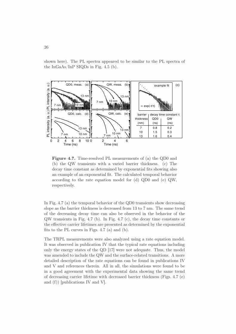
26
shown here). The PL spectra appeared to be similar to the PL spectra ofthe InGaAs/InP SIQDs in Fig. 4.5 (b).
barrier decay time constantthickness QD0 QW (nm) (ns) (ns)
13 nm
10 nm
QW, meas. (b)
7 nm
7 0.8 0.2 10 1.5 0.3 13 1.6 0.4
0 2 4 6
13 nm
QW, calc. (e)
7 nm10 nm
Time (ns)
13 nm
10 nm
QD0, meas. (a)
7 nm
PL
inte
nsity
(a.
u.)
0 2 4 6 8 10
PL
inte
nsity
(a.
u.)
Time (ns)
13 nm
QD0, calc. (d)
7 nm 10 nm
∝ exp(-t/τ)
(c)
example fit
τ
Figure 4.7. Time-resolved PL measurements of (a) the QD0 and(b) the QW transients with a varied barrier thickness. (c) Thedecay time constant as determined by exponential fits showing alsoan example of an exponential fit. The calculated temporal behavioraccording to the rate equation model for (d) QD0 and (e) QW,respectively.
In Fig. 4.7 (a) the temporal behavior of the QD0 transients show decreasingslope as the barrier thickness is decreased from 13 to 7 nm. The same trendof the decreasing decay time can also be observed in the behavior of theQW transients in Fig. 4.7 (b). In Fig. 4.7 (c), the decay time constants orthe effective carrier lifetimes are presented as determined by the exponentialfits to the PL curves in Figs. 4.7 (a) and (b).
The TRPL measurements were also analyzed using a rate equation model.It was observed in publication IV that the typical rate equations includingonly the energy states of the QD [17] were not adequate. Thus, the modelwas amended to include the QW and the surface-related transitions. A moredetailed description of the rate equations can be found in publications IVand V and references therein. All in all, the simulations were found to bein a good agreement with the experimental data showing the same trendof decreasing carrier lifetime with decreased barrier thickness (Figs. 4.7 (e)and (f)) [publications IV and V].

27
Relaxation of carriers from a higher energy state to a lower state (carrierfeeding) plays an important role in this kind of a multilevel energy structure.Basically, the levels are emptied one by one starting from the highest energylevel. As reported for InGaAs/GaAs SIQDs, carrier feeding can cause some-what similar plateau-like behavior [17] as seen in Fig. 4.7. However, it waspointed out in publication V that carrier feeding alone does not explain theevident dependency of the carrier lifetime on the barrier thickness observedin Fig. 4.7. Moreover, the fact that decreasing the barrier thickness resultsin a shorter decay time for both the QD0 and QW levels indicates thatthe increased non-radiative recombination in the QW and QDs is causedby surface-related effects. It seems likely that carriers might be capturedby the stressor islands on the surface due to the lower band gap of InAs.Carriers in the islands could then recombine radiatively or experience non-radiative recombination via surface states. For simplicity, in the following,these processes are referred to as surface capture.
In the latter part of the QD0 curves, carrier feeding from the higher energylevel becomes more and more insignificant meaning that the decay timeis mostly determined by the radiative recombination and surface capture.Thus, the decay time constant determined from the experimental PL curvedefines the lower limit for the time constant of the radiative recombination.For example, with a barrier thickness of 7 nm this lower limit is 0.8 ns.
As mentioned previously, the time-resolved PL of the InGaAs/GaAs SIQDsutilizing InP stressors has been shown to be unaffected by the variationof the barrier thickness. The QW PL intensity, however, was reported todiminish with decreased barrier thickness. Since the InP layer has beenreported to passivate the GaAs surface [28], it has been presumed that theInP islands protect the strain-induced QD [19]. On the other hand, it hasbeen reported that the surface depletion is suppressed and that surface bandbending occurs in the region beneath the InAs/InP and the InAs/GaAsislands [57–59]. Same studies have shown, however, that an InAs wettinglayer does not have such a significant effect. Since between the InAs stressorislands on InP there is most likely a thin InAs wetting layer, the effect ofthe wetting layer was also discussed in publication V. Near-surface QWstructures (similar to the ones in SIQDs) were used as reference samples.Instead of growing InAs islands, only a thin layer of InAs was depositedon the surface to form a wetting layer without islands. A near-surface QWwith no InAs was also fabricated for reference. TRPL transients of thesamples with or the samples without the InAs wetting layer were virtuallythe same. This showed that wetting does not increase surface recombinationsignificantly. With these observations, it was concluded in publication V

28
that the carriers captured away from the QW and QDs are mostly tunneledto the InAs islands on the surface.
7 10 13
0.1
1
10
(c)(b)
QW
Sur
face
cap
ture
tim
e (n
s cm
-2)
Barrier thickness (nm)
QD0
(a)
7 10 130.1
1
10
QW
QD0
Rec
ombi
natio
n tim
e (n
s)
Barrier thickness (nm)7 10 13
20
40
60
80100
QD
cap
ture
tim
e (n
s cm
-2)
Barrier thickness (nm)
Figure 4.8. (a) Surface capture time constants, (b) QD capturetime constants and (b) recombination time constants obtained forthe QW and the QD0 from the rate equation model.
Figs. 4.8 (a) and (b) show surface capture and QD capture time constantsobtained from the rate equation analyses in publications IV and V. Surfacecapture time constant increases (i.e., the capture probability decreases) byan order of magnitude as the barrier thickness is increased from 7 to 13 nm.It should be also noted that the probability of an electron to experience sur-face capture from the QW is over ten times larger as compared to the QD.As mentioned in chapter 4.1.2, 80 – 90 % of the redshift originates from theconduction band [publication III]. Thus, in the InGaAsP/InP QDs studiedin publication V, the QW ground state for an electron is approximately50 meV higher than the QD ground state (redshift is ∼55 meV). In otherwords, spatially under the stressor, an electron at the QW ground state ex-periences effectively ∼50 meV smaller barrier to the surface. This differencein the barrier height provides a plausible explanation for the smaller surfacecapture time constant observed for the QW compared to that of the QD0in Fig. 4.8 (a).
The recombination time constants of the QD0 and QW peaks in Fig. 4.8 (c)do not show any significant dependence on the barrier thickness. The re-combination time constant reported for InGaAs/GaAs SIQDs (0.86 ns [14])is roughly the same as determined for InGaAsP/InP SIQDs with a barrierthickness of 7 nm in publication V (0.9 ns). Moreover, it also agrees withthe lower limit (0.8 ns) determined above from the experimental TRPLmeasurement.

29
4.2 InAs nanorings on InP
4.2.1 Fabrication of self-assembled nanorings
It was previously reported in this thesis that the growth of InAs islands onInP was affected by the As/P exchange. It caused an undesired increasein the height of the islands. The As/P exchange process can, however,also be exploited in the fabrication of self-assembled structures. Insteadof relying on the typical partial capping approach of nanoring fabrication,annealing in TBP was demonstrated to transform uncapped self-assembledInAs islands on InP into NRs in publication VI. This novel fabricationmethod is advantageous since the capping layer is no longer an integral partof the transformation process. Therefore, the transformation and cappingcan be optimized individually. Altogether, this potential can be capitalizedin the investigation and design of NR structures and devices.
The fabrication process to create nanorings by annealing self-assembledislands introduced in this thesis is as follows. After the semi-insulatingInP(001) substrate was annealed for 5 min at 650
◦
C, a 100-nm InP bufferlayer was grown at 640
◦
C. Self-assembled islands were subsequently grownby depositing 0.6 – 1.0 MLs of InAs at 560
◦
C. Islands were then stabilizedin TBAs for 10 s. In order to transform islands to rings the TBAs flow wasswitched to TBP. Reference samples were also fabricated by cooling downthe deposited islands in TBAs (as-grown islands). [publication VI]
Fig. 4.9 (a) shows AFM images of the reference as-grown islands (top) andNRs formed utilizing a TBP anneal at 560
◦
C for 9 s (bottom). The differ-ence in the morphology of an island (dotted line) and a NR (solid line) canbe seen more clearly in the cross-sectional AFM profiles in Fig. 4.9 (b). Theheight of the island is approximately 30 nm whereas the height of the NRis only 10 nm. Moreover, it should be noted that the NR shows a distinctcenter hole with a diameter comparable to the island width (∼90 nm). Thisindicates that most of the island material has moved outward from the ini-tial island location. Although the lateral sizes of the features are somewhatexaggerated due to the finite curvature of the AFM tip, the island and NRvolumes were estimated to be roughly the same in publication VI. The arealdensity of the nanorings (and the islands) was typically ∼108 cm2.
The following conclusions were made in publication VI concerning theisland-to-ring transformation process applied in this thesis compared to theprevious studies (reviewed in section 3.3): Since no capping is applied, the

30
0 100 200 300 400 500 600
0
5
10
15
20
25
30
35
nanoring
island
Hei
ght (
nm)
Lateral distance (nm)
100 nm
320 nm
100 nm
13 nm
30 nm
(a) (b)islands
nanorings
Figure 4.9. (a) Atomic force micrographs (1.4 µm × 1.4 µm) ofInAs islands (top) and NRs (bottom). Note the different verticalscales. (b) AFM cross-section profiles of an InAs island (dottedline) and a NR (solid line).
thermodynamic model (which is based on the changes in surface free energycaused by the cap layer) was not considered to provide a plausible explana-tion for the transformation. The difference in group III surface mobilities(kinetic model [42, 43, 45]) does not provide an explanation either, becauseboth materials have the same group III atom in the InAs/InP system.
Interestingly, the partial capping technique has also been used to fabricateInAs/InP NRs [44]. The kinetic model proposed for InAs/GaAs NRs wasfound to disagree with the results. Thus, the shape transformation wasconsidered to be explained by the thermodynamic model. It should bementioned that As/P exchange was not considered in that report in anyway.
The As/P exchange has been shown to have a strong effect on InAs nanos-tructures on InP [49, 52, 60]. Furthermore, Ga atoms have been shown tomigrate away from the top surface of partially relaxed InAs/GaAs islandsdue the chemical potential [48]. SiGe/Si [47] and InAs/InP [49] NR studiesutilizing partial capping technique have also shown the significance of thestrain distribution in the transformation process. Thus, it is conceivablethat InP formed at the surface of InAs island by As/P exchange wouldexperience strain-driven migration away from the island [publication VI].
31
TBP
P As1o
TBP
P As2o
TBP P As
3o
In
InAs QD
InP
InAs(P) NR
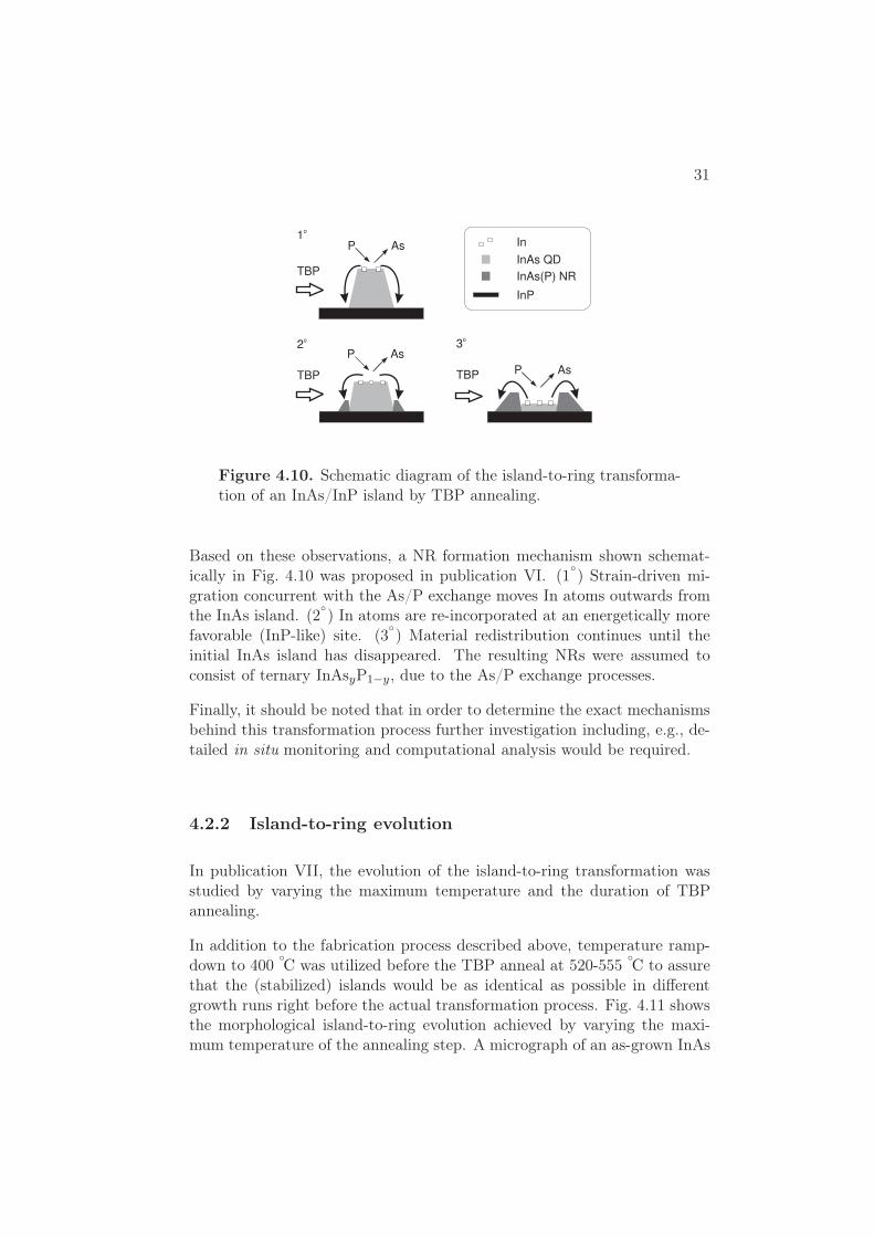
Figure 4.10. Schematic diagram of the island-to-ring transforma-tion of an InAs/InP island by TBP annealing.
Based on these observations, a NR formation mechanism shown schemat-ically in Fig. 4.10 was proposed in publication VI. (1
◦
) Strain-driven mi-gration concurrent with the As/P exchange moves In atoms outwards fromthe InAs island. (2
◦
) In atoms are re-incorporated at an energetically morefavorable (InP-like) site. (3
◦
) Material redistribution continues until theinitial InAs island has disappeared. The resulting NRs were assumed toconsist of ternary InAsyP1−y, due to the As/P exchange processes.
Finally, it should be noted that in order to determine the exact mechanismsbehind this transformation process further investigation including, e.g., de-tailed in situ monitoring and computational analysis would be required.
4.2.2 Island-to-ring evolution
In publication VII, the evolution of the island-to-ring transformation wasstudied by varying the maximum temperature and the duration of TBPannealing.
In addition to the fabrication process described above, temperature ramp-down to 400
◦
C was utilized before the TBP anneal at 520-555◦
C to assurethat the (stabilized) islands would be as identical as possible in differentgrowth runs right before the actual transformation process. Fig. 4.11 showsthe morphological island-to-ring evolution achieved by varying the maxi-mum temperature of the annealing step. A micrograph of an as-grown InAs

32
10 nm
(d)
10 nm
(c)
10 nm
(b)
40 nm
(a)
Figure 4.11. Atomic force micrographs (0.5×0.5 µm2) of (a) as-grown InAs island, and island annealed in TBP at (b) 520, (c) 540,and (d) 555
◦
C. Note the different height scales.
island is shown in Fig. 4.11 (a). Fig. 4.11 (b) shows an island annealed at520
◦
C. It can be observed that the height (∼10 nm) is clearly reducedwhile the diameter is increased notably. It seems that the island material isdistributed around the original island location. Fig. 4.11 (c) shows that theformation of the center hole has started during the TBP anneal at 540
◦
C. Adistinct NR seen in Fig. 4.11 (d) results from the annealing step at 555
◦
C.[publication VII]
The morphological evolution was studied in publication VII by varying theduration of the annealing step. Fig. 4.12 (a) shows the cross-sectional AFMprofiles of the samples annealed at 550
◦
C for 12, 18, and 35 s. The heightof the island is already reduced after 12 s of annealing, but the top surfaceis still quite flat. It resembles the island shown in Fig. 4.11 (b). However,a notable transformation towards NR profile is produced by 18 s of TBPannealing. Finally, the center hole extends to the surrounding buffer levelafter 35 s of annealing. This shows that most of the material from the initialInAs island has been redistributed.
Optical properties of the NRs were also studied in publication VII. A sim-ilar set of samples as characterized in Fig. 4.12 (a) was fabricated for thePL measurements by growing a 20-nm InP capping layer on top of theNRs. Fig. 4.12 (b) shows PL spectra of the samples with a varied anneal-ing time (12, 18, and 35 s). It should be noted that the Ge detector usedin the measurements cuts off most of the luminescence below 0.75 eV (thearea is indicated with shading in Fig. 4.12 (b)). Nevertheless, it can beobserved that the PL is blueshifted along with increased anneal time. Itwas concluded in publication VII that since the height of the NRs doesnot change significantly after 12 s of annealing, the blueshift occurs likely

33
0 100 200 300 400
0
3
6
9
12
15(a)
TBPanneal
35 s
18 s
12 s
Hei
ght (
nm)
Lateral distance (nm)
0.7 0.8 0.9 1.0 1.1
TBPanneal
detectorcut-off
(b)T=10 K
35 s
18 s
12 s
PL
inte
nsity
(a.
u.)
Energy (eV)
Figure 4.12. (a) AFM cross-section profiles and (b) PL spectraof NRs fabricated at 550
◦
C with a varied TBP anneal time. Theshaded area on the left represents the response cut-off region of theGe detector. The curves are offset vertically for clarity.
due to a compositional change in the NR material. It is conceivable thatthe low-energy side of the luminescence might originate from the As-richregion while the P-rich region is responsible for the high-energy lumines-cence. These observations support the assumption made in publication VIthat the transformation of an InAs/InP island into a NR is accompaniedby a compositional change of InAs to InAsP.
4.3 GaN passivation of GaAs surface
GaN is a wide band gap (3.4 eV) III-V semiconductor and it is consideredto have a rather high thermal and chemical stability. It is very attractivematerial since it can be used to fabricate, e.g., blue LEDs and laser diodes[61, 62]. Typically, hexagonal GaN is grown on a sapphire substrate attemperatures around 1000
◦
C [63, 64]. On the other hand, cubic GaN canbeen grown on GaAs(100) substrates using temperatures around 550
◦
C [65,66]. However, threading dislocations inflicted by the large lattice mismatch(∼20 %) between GaN and GaAs are problematic since they destroy thecharacteristics of the devices in most cases. This problem can be avoidedby using ultrathin layers (few monolayers) of GaN, which are below theso-called critical thickness. This kind of ultrathin layer is not suitable formost of the optoelectronic applications. However, the stability of GaN can

34
be still exploited by using it, e.g., as a protective passivation layer on topof a structure to prevent surface recombination of charge carriers.
Different passivation techniques have been studied in order to reduce thedensity of surface states. GaP formed by As-P exchange reaction, native ox-ides, standard Si-based insulators (SiO2 and Si3N4), and a variety of plasmanitridation methods have been demonstrated to passivate GaAs surfaces[67, 68]. The use of different plasma methods has faced problems with, e.g.,disordered surface leading to deep donor states, and formation of mixtureof GaN and Ga2O3 instead of pure GaN [69].
Passivation techniques using plasma are ex situ methods for most of theMOVPE systems. Although ex situ methods are useful if the structures areto be processed anyway, in situ surface passivation has been considered tobe the most effective way to reduce the surface state density of epitaxiallayers. For example, only 1 ML of InP has been shown to be effective in thepassivation of AlGaAs/GaAs near-surface QWs [70–72]. Moreover, as men-tioned previously, the InGaAs/GaAs SIQDs experience virtually no surfacerecombination due to the protective nature of the InP stressor islands [19].
MOVPE growth of epitaxial GaN on GaAs is enabled by the use of dimethyl-hydrazine as a nitrogen source. The low decomposition temperature ofDMHy allows growth at temperatures around 550
◦
C [73]. Hence, the ac-tive structure will not suffer from additional heating during the passivationas the typical growth temperature of the GaAs-based materials is around650
◦
C. In publication IX, the passivation of the GaAs surface by an epi-taxial ultrathin GaN layer was studied. The growth procedures of GaN onGaAs [66], on the other hand, were based on the results of publication VIII.
A rather straightforward and sensitive method to assess the effect of thepassivation is to optically probe the characteristics of a near-surface QW.Carriers from the near-surface QW are tunneled quite easily into possiblesurface states and that can be observed as a reduction of the PL intensity.As a result, while using identical near-surface QWs in a set of samples,the PL intensity gives an indication about efficiency of the passivation. Inpublication IX low-temperature photoluminescence was used to study theeffect of passivation on InGaAs/GaAs near-surface QWs. Fig. 4.13 (a) showsthe schematic structure of a passivation sample.
Prior to the growth of the QW structures, semi-insulating GaAs(100) sub-strates were annealed in the MOVPE reactor at 700
◦
C for 5 min to removethe native oxide. The InxGa1−xAs QW was fabricated at 650
◦
C on a 100-nm-thick GaAs buffer layer and was capped by 5 nm of GaAs. The thickness

35
process step
time (s)
group V flowGaAs cap
TBAs
0
TBAscool-down
15
nitridationDMHy
85
RT
Tem
pera
ture
H2
650 C
600 C
400 Csubstrate
GaAsInGaAs QWGaAs
passivation
(a) (b)
Figure 4.13. (a) Near-surface QW structure used in passivationsamples and (b) schematic plot of the post-growth nitridation pro-cedure (axes not in scale).
of the QW was 4 or 6 nm and the indium fraction x used was 20 or 25 %,respectively. Finally, the passivation layer was grown.
In publication VIII, a 5-period GaN/GaAs superlattice was used as atest structure in order to investigate the growth of GaN layers. A two-temperature growth process was found to yield good crystal quality andatomically flat surfaces. Based on these results, two different surface passi-vation methods using DMHy were employed.
In the first method, a thin GaN layer (nominally 1 – 3 MLs) was grown at550
◦
C. In the second method, shown in Fig. 4.13 (b), after the growthof the top barrier GaAs layer, the TBAs flow was switched to DMHy at600
◦
C to form a thin GaN layer via arsenic-to-nitrogen (As/N) exchange.After approximately 70 s of cooling, the DMHy protection was switched offat 400
◦
C. For reference, a similar near-surface QW structure was grownwithout passivation. A deep-QW sample with a 20-nm-thick GaAs topbarrier layer was also used as a reference.
It was observed in publication IX that the PL intensity of the as-grownGaN passivated sample was enhanced by a factor of 21 compared to theunpassivated QW. Moreover, the integrated intensity of the as-grown GaN-passivated sample was nearly the same as compared to the deep QW sample.This indicates that the ultrathin GaN layer passivates the GaAs surfaceeffectively.
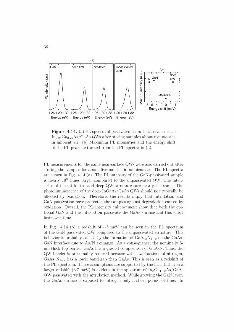
36
1.26 1.29 1.32
(a)
PL
inte
nsity
(a.
u.)
Energy (eV)
GaN
1.26 1.29 1.32
Energy (eV)
deep QW
1.26 1.29 1.32
Energy (eV)
nitridated
1.26 1.29 1.32
Energy (eV)
unpassivatedx400
-8 -6 -4 -2 0 2 4
(b)
Energy shift (meV)
Max
. PL
inte
nsity
(a.
u.)
N GaN
unpassiv.
deepQW
Figure 4.14. (a) PL spectra of passivated 4-nm-thick near-surfaceIn0.25Ga0.75As/GaAs QWs after storing samples about five monthsin ambient air. (b) Maximum PL intensities and the energy shiftof the PL peaks extracted from the PL spectra in (a).
PL measurements for the same near-surface QWs were also carried out afterstoring the samples for about five months in ambient air. The PL spectraare shown in Fig. 4.14 (a). The PL intensity of the GaN-passivated sampleis nearly 103 times larger compared to the unpassivated QW. The inten-sities of the nitridated and deep-QW structures are nearly the same. Thephotoluminescence of the deep InGaAs/GaAs QWs should not typically beaffected by oxidation. Therefore, the results imply that nitridation andGaN passivation have protected the samples against degradation caused byoxidation. Overall, the PL intensity enhancement show that both the epi-taxial GaN and the nitridation passivate the GaAs surface and this effectlasts over time.
In Fig. 4.14 (b) a redshift of ∼5 meV can be seen in the PL spectrumof the GaN passivated QW compared to the unpassivated structure. Thisbehavior is probably caused by the formation of GaAsxN1−x on the GaAs-GaN interface due to As/N exchange. As a consequence, the nominally 5-nm-thick top barrier GaAs has a graded composition of GaAsN. Thus, theQW barrier is presumably reduced because with low fractions of nitrogen,GaAsxN1−x has a lower band gap than GaAs. This is seen as a redshift ofthe PL spectrum. These assumptions are supported by the fact that even alarger redshift (∼7 meV) is evident in the spectrum of InxGa1−xAs/GaAsQW passivated with the nitridation method. While growing the GaN layer,the GaAs surface is exposed to nitrogen only a short period of time. In

37
the nitridation, on the other hand, the GaAs surface is exposed during thewhole process allowing more effective As/N exchange on the surface. Thismeans that in the nitridation process more nitrogen is diffused deeper intothe GaAs barrier, effectively leading to even larger reduction of the QWbarrier.
It was also noted in publication IX that the AFM micrographs showed nosignificant differences between the epitaxial GaN layer and the nitridatedGaAs surface. Moreover, the passivation treatments do not seem to degradethe surface morphology of the GaAs. All in all, the results in publication IXsuggest that the ultrathin epitaxial GaN layer grown on GaAs is an efficientin situ method for surface passivation.

5 Summary
Self-assembled nanostructures are of particular interest in semiconductortechnology, since they have novel quantum mechanical properties and theyoffer new functionality or improved performance for applications. A typicalapproach is to bury self-assembled islands in another semiconductor with alarger band gap to create QDs, which are applicable, e.g., in optoelectronics.Alternatively, self-assembled islands can be used as stressors on top of anear-surface QW in order to create strain-induced QDs or stressor QDswithin the QW.
In this thesis, the main focus was in the fabrication and characterization ofself-assembled III-V compound semiconductor nanostructures. Firstly, self-assembled InAs islands were used to produce stressor QDs. Secondly, InAsislands were transformed into nanorings. Thirdly, in situ grown epitaxialGaN layers were used to passivate GaAs surfaces. The samples studiedin this thesis were fabricated by MOVPE. AFM was used to study thesize and areal density of the InAs islands as well as the morphology ofthe nanorings. Low-temperature PL measurements were used to study theoptical characteristics of the samples.
A new material system utilizing InAs stressor islands to create In-GaAs(P)/InP strain-induced QDs was demonstrated. The wavelength ofthe QD ground state luminescence was tuned in the range of 1.3 – 1.7 µmby varying the QW composition. The island ensemble was optimized us-ing a temperature ramp-down to reduce the uncontrolled accumulation ofmaterial trough arsenic-to-phosphorus exchange. Modification of the QDconfinement potential by varying the height of the islands (from 15 to 30nm) or by decreasing the distance of the QW from the surface (from 13 to 4nm) was observed to increase the energy separation (PL redshift) of the QDand QW ground states approximately by 20 meV. Moreover, it was foundthat the most feasible size of the stressor islands is around 15 to 30 nmin height. Based on the time-resolved PL measurements, it was concludedthat the lifetime of carriers in the QD was reduced by the carrier capture of
38

39
stressor islands on the surface. However, the results show that the surfacecapture rate can be decreased considerably by controlling the distance ofthe QW from the surface. All in all, PL spectra showed a typical spacingof 15 meV between the QD peaks, a FWHM as narrow as 11 meV for theQD peaks, and a redshift of the QD ground state peak from the QW peakas large as 70 meV.
Previously, self-assembled nanorings have been typically fabricated by trans-forming self-assembled islands into nanorings utilizing a partial cappinglayer and a subsequent annealing step. In the method introduced in thisthesis, however, no capping was used. Instead, the island-to-ring trans-formation was achieved by annealing the self-assembled InAs islands in aphosphorous ambient. It was assumed that the material redistribution, i.e.,the transformation, was caused by the arsenic-to-phosphorus exchange alongwith the strain-driven migration of In atoms outwards from the island.
Passivation of a GaAs surface by an epitaxial ultrathin GaN layer was stud-ied in order to reduce the density of surface states. The GaN layers weregrown in situ on the top of near-surface InGaAs/GaAs QWs. The effectof the surface passivation was determined by comparing the PL intensities.Significant enhancement of the PL intensity due to passivation showed thatthe ultrathin epitaxial GaN layer grown on GaAs is an efficient method forsurface passivation.

References
[1] M. E. Heimbuch, A. L. Holmes, Jr., C. M. Reaves, M. P. Mack, S. P.DenBaars, and L. A. Coldren, J. Electron Mater. 23, 87 (1994).
[2] G. Binning, C. F. Quate, and C. Gerbe, Phys. Rev. Lett. 56, 930(1986).
[3] G. W. Bryant, Phys. Rev. B 37, 8763 (1988).
[4] F. C. Frank and J. H. van der Merwe, Proc. Roy. Soc. London A198,216 (1949).
[5] M. Volmer and A. Weber, Z. Physik. Chem. 119, 277 (1926).
[6] I. N. Stranski and L. Krastanow, Sitz. Ber. Akad. Wiss., Math.-naturwiss. Kl. Abt. IIb 146, 797 (1938).
[7] D. J. Eaglesham and M. Cerullo, Phys. Rev. Lett. 64, 1943 (1990).
[8] M. A. Reed, R. T. Bate, K. Bradshaw, W. M. Duncan, W. R. Frensley,J. W. Lee, and H. D. Shih, J. Vac. Sci. Technol. B 4, 358 (1986).
[9] K. Kash, A. Scherer, J. M. Worlock, H. G. Craighead, and M. C.Tamargo, Appl. Phys. Lett. 49, 1043 (1986).
[10] K. Kash, J. M. Worlock, M. D. Sturge, P. Grabbe, J. P. Harbison,A. Scherer, and P. Lin, Appl. Phys. Lett. 53 (1988).
[11] M. Sopanen, H. Lipsanen, and J. Ahopelto, Appl. Phys. Lett. 66, 2364(1995).
[12] H. Lipsanen, M. Sopanen, and J. Tulkki, a review chapter 4 OpticalProperties of Quantum Dots Induced by Self-Assembled Stressors inOptics of Quantum Dots and Wires, edited by G. W. Bryant and G. S.Solomon (Artech House Inc., Norwood, MA, USA, 2005).
40

41
[13] J. Tulkki and A. Heinämäki, Phys. Rev. B 51, 8239 (1995).
[14] M. Brasken, M. Lindberg, and J. Tulkki, phys. stat. sol. A 164, 427(1997).
[15] U. Bockelmann and T. Egeler, Phys. Rev. B 46, 15574 (1992).
[16] M. Brasken, M. Lindberg, M. Sopanen, H. Lipsanen, and J. Tulkki,Phys. Rev. B 58, R15993 (1998).
[17] S. Grosse, J. H. H. Sandmann, G. von Plessen, J. Feldmann, H. Lipsa-nen, M. Sopanen, J. Tulkki, and J. Ahopelto, Phys. Rev. B 55, 4473(1997).
[18] H. Lipsanen, M. Sopanen, and J. Ahopelto, Phys. Rev. B 51, 13868(1995).
[19] C. Lingk, W. Helfer, G. von Plessen, J. Feldmann, K. Stock, M. W.Feise, D. S. Citrin, H. Lipsanen, M. Sopanen, R. Virkkala, J. Tulkki,and J. Ahopelto, Phys. Rev. B 62, 13588 (2000).
[20] M. Grundmann, R. Heitz, D. Bimberg, and J. H. H. Sandmann, phys.stat. sol. (b) 203, 121 (1997).
[21] J. Ahopelto, M. Sopanen, and H. Lipsanen, Jpn. J. Appl. Phys. 38,1081 (1999).
[22] H. Koskenvaara, T. Hakkarainen, H. Lipsanen, and M. Sopanen, J.Mat. Sci. 14, 357 (2003).
[23] M. Sopanen, M. Taskinen, H. Lipsanen, and J. Ahopelto, Appl. Phys.Lett. 69, 3393 (1996).
[24] M. C. Hanna, Z. H. Lu, A. F. Cahill, M. J. Heben, and A. J. Nozik, J.Cryst. Growth 174, 605 (1997).
[25] T. Wang and A. Forchel, Appl. Phys. Lett. 73, 1847 (1998).
[26] E. S. Kim, N. Usami, and Y. Shiraki, Appl. Phys. Lett. 70, 295 (1997).
[27] W. V. Schoenfeld, C. Metzner, E. Letts, and P. M. Petroff, Phys. Rev.B 63, 205319 (2001).
[28] H. Lipsanen, M. Sopanen, M. Taskinen, J. Tulkki, and J. Ahopelto,Appl. Phys. Lett. 68, 2216 (1996).
[29] T. Wang and A. Forchel, J. Appl. Phys. 86, 2001 (1999).

42
[30] N. N. Ledentsov, J. Böhrer, M. Beer, F. Heinrichsdorff, M. Grundmann,D. Bimberg, S. V. Ivanov, B. Y. Meltser, S. V. Shaposhnikov, I. N.Yassievich, N. N. Faleev, P. S. Kop’ev, and Zh. I. Alferov, Phys. Rev.B 52, 14058 (1995).
[31] M. Bayer, M. Korkusinski, P. Hawrylak, T. Gutbrod, M. Michel, andA. Forchel, Phys. Rev. Lett. 90, 186801 (2003).
[32] Y. Aharonov and D. Bohm, Phys. Rev. 115, 485 (1959).
[33] D. Mailly, C. Chapelier, and A. Benoit, Phys. Rev. Lett. 70, 2020(1993).
[34] R. J. Warburton, C. Schäflein, D. Haft, A. L. F. Bickel and, K. Kar-rai, J. M. Garcia, W. Schoenfeld, and P. M. Petroff, Nature 405, 926(2000).
[35] A. Lorke, R. J. Luyken, A. O. Govorov, J. P. Kotthaus, J. M. Garcia,and P. M. Petroff, Phys. Rev. Lett. 84, 2223 (2000).
[36] F. Suárez, D. Granados, M. L. Dotor, and J. M. García, Nanotechnol-ogy 15, S126 (2004).
[37] A. Y. Nazzal, H. Fu, and L.-W. Wang, J. Appl. Phys. 98, 083703(2005).
[38] P. A. Orellana and M. Pacheco, Phys. Rev. B 71, 235330 (2005).
[39] T. Chakraborty and P. Pietiläinen, Phys. Rev. B 50, 8460 (1994).
[40] T. W. Kim, E. H. Lee, K. H. Lee, J. S. Kim, and H. L. Park, Appl.Phys. Lett. 84, 595 (2004).
[41] S. Kobayashi, C. Jiang, T. Kawazu, and H. Sakaki, Jpn. J. Appl. Phys.43, L662 (2004).
[42] A. Lorke, R. Blossey, J. M. Garcia, M. Bichler, and G. Abstreiter, Mat.Sci. Eng. B 88, 225 (2002).
[43] A. Lorke, R. J. Luyken, J. M. Garcia, and P. M. Petroff, Jpn. J. Appl.Phys. 40, 1857 (2001).
[44] T. Raz, D. Ritter, and G. Bahir, Appl. Phys. Lett. 82, 1706 (2003).
[45] J. M. Garcia, G. Medeiros-Ribeiro, K. Schmidt, T. Ngo, J. L. Feng,A. Lorke, J. Kotthaus, and P. M. Petroff, Appl. Phys. Lett. 71, 2014(1997).

43
[46] R. Blossey and A. Lorke, Phys. Rev. E 65, 021603 (2002).
[47] J. Cui, Q. He, X. M. Jiang, Y. L. Fan, X. J. Yang, F. Xue, and Z. M.Jiang, Appl. Phys. Lett. 83, 2907 (2003).
[48] Q. Xie, P. Chen, and A. Madhukar, Appl. Phys. Lett. 65, 2051 (1994).
[49] P. J. Poole, R. L. Williams, J. Lefebvre, and S. Moisa, J. Cryst. Growth257, 89 (2003).
[50] S. Yoon, Y. Moon, T.-W. Lee, E. Yoon, and Y. D. Kim, Appl. Phys.Lett. 74, 2029 (1999).
[51] B. Wang, F. Zhao, Y. Peng, Z. Jin, Y. Li, and S. Liu, Appl. Phys. Lett.72, 2433 (1998).
[52] H. R. Gutiérrez, M. A. Cotta, J. R. R. Bortoleto, and M. M. G. de Car-valho, J. Appl. Phys. 92, 7523 (2002).
[53] W. Seifert, N. Carlsson, J. Johansson, M.-E. Pistol, and L. Samuelson,J. Cryst. Growth 170, 39 (1997).
[54] N. Carlsson, T. Junno, L. Montelius, M.-E. Pistol, L. Samuelson, andW. Seifert, J. Cryst. Growth 191, 347 (1998).
[55] M. A. Cotta, C. A. C. Mendonca, E. A. Meneses, and M. M. G. Car-valho, Surf. Sci. 388, 84 (1997).
[56] P. Jin, X. Q. Meng, C. M. L. Z. Y. Zhang, F. Q. L. B. Xu, Z. G. Wang,Y. G. Li, C. Z. Zhang, and S. H. Pan, J. Appl. Phys. 93, 4169 (2003).
[57] K. O. Vicaro, M. A. Cotta, H. R. Gutiérrez, and J. R. R. Bortoleto,Nanotech. 14, 509 (2003).
[58] I. Tanaka, I. Kamiya, H. Sakaki, N. Qureshi, J. S. J. Allen, and P. M.Petroff, Appl. Phys. Lett. 74, 844 (1999).
[59] T. Takahashi, M. Yoshita, I. Kamiya, and H. Sakaki, Appl. Phys. A66, S1055 (1998).
[60] M. Taskinen, M. Sopanen, H. Lipsanen, J. Tulkki, T. Tuomi, andJ. Ahopelto, Surf. Sci. 376, 60 (1997).
[61] S. Nakamura, J. Mater. Res. 14, 2716 (1999).
[62] T. Mukai and S. Nakamura, Jpn. J. Appl. Phys 38, 5735 (1999).
[63] I. Akasaki, H. Amano, Y. Koide, K. Hiramatsu, and N. Sawaki, J.Crystal Growth 98, 209 (1989).
[64] K. Hiramatsu, S. Itoh, H. Amano, I. A. Kuwano, T. Shiraishi, andK. Oki, J. Cryst. Growth 115, 628 (1991).
[65] H. Yang, O. Brandt, A. Trampert, and K. H. Ploog, Appl. Surf. Sci.104/105, 461 (1996).
[66] J. Sormunen, J. Toivonen, M. Sopanen, and H. Lipsanen, Appl. Surf.Sci. 222, 286 (2004).
[67] M. Losurdo, P. Capezzuto, and G. Bruno, Appl. Phys. Lett. 81, 16(2002).
[68] S. Anantathanasarn and H. Hasegawa, Appl. Surf. Sci. 190, 343 (2002).
[69] S. Anantathanasarn, S.-Y. Oomoto, T. Hashizume, and H. Hasegawa,Appl. Surf. Sci. 159/160, 456 (2000).
[70] Y. Wada and K. Wada, Appl. Phys. Lett. 63, 379 (1993).
[71] Y. Wada and K. Wada, J. Vac. Sci. Technol. B 12, 3084 (1994).
[72] H. Lipsanen, M. Sopanen, M. Taskinen, J. Tulkki, and J. Ahopelto,Appl. Phys. Lett. 68, 2216 (1996).
[73] H. Sato, H. Takahashi, A. Watanabe, and H. Ota, Appl. Phys. Lett.68, 3617 (1996).