x2-cx4 data sheet04-general - fujitsu global number: fcu-022m101 (mid-pak type) features z compliant...
TRANSCRIPT
xx--mmGGCC,, EElleeccttrriiccaall TTrraannsscceeiivveerr ffoorr 1100GGBBAASSEE--CCXX44
Fujitsu Component Limited Page 1 of 24
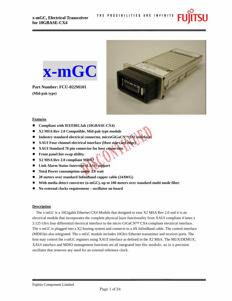
x-mGC
Part Number: FCU-022M101 (Mid-pak type)
Features
Compliant with IEEE802.3ak (10GBASE-CX4) X2 MSA Rev 2.0 Compatible, Mid-pak type module Industry standard electrical connector, microGiGaCNTM (I/O interface) XAUI Four channel electrical interface (Host side card edge) XAUI Standard 70 pin connector for host connection Front panel hot swap ability. X2 MSA Rev 2.0 compliant MDIO Link Alarm Status Interrupt (LASI) support Total Power consumption under 3.0 watt 20 meters over standard InfiniBand copper cable (24AWG) With media detect converter (o-mGC), up to 100 meters over standard multi mode fiber. No external clocks requirement – oscillator on board
Description The x-mGC is a 10Gigabit Ethernet CX4 Module that designed to ease X2 MSA Rev 2.0 and it is an
electrical module that incorporates the complete physical layer functionality from XAUI compliant 4 lanes x 3.125 Gb/s four differential electrical interface to the micro GiGaCN™ CX4 compliant electrical interface. The x-mGC is plugged into a X2 hosting system and connects to a 4X InfiniBand cable. The control interface (MDIO)is also integrated. The x-mGC module includes 10Gb/s Ethernet transmitter and receiver ports. The host may control the x-mGC registers using XAUI interface as defined in the X2 MSA. The MUX/DEMUX, XAUI interface and MDIO management functions are all integrated into the module, as is a precision oscillator that removes any need for an external reference clock.

xx--mmGGCC,, EElleeccttrriiccaall TTrraannsscceeiivveerr ffoorr 1100GGBBAASSEE--CCXX44
Fujitsu Component Limited Page 2 of 24
x-mGC Block Diagram
7
Figure 1: Functional Brock Diagram of x-mGC module
(*1) In case of InfiniBand cable is connected, the power does not supply to cable, and if o-mGC is connected,
a ground contact is changed Vcc for power supply to o-mGC by Media detect function.
Absolute Maximum Ratings Parameter Min Typ Max Units Notes
Storage Temperature -20 60 ℃ Storage Humidity 0 80 % Wet bulb 38℃ Supply Voltage(3.3V) 3.135 3.3 3.465 V Adaptable Power Supply(1.5V) 1.425 1.5 1.575 V Voltage on LVCMOS pins 1.2 V
Recommended Operating Conditions Parameter Min Typ Max Units Notes
Operating Temperature 0 50 ℃ Operating Humidity 0 80 % Wet bulb 38℃
General Electrical Specification
Interface: XAUI side; 70 pin SMT connector (See X2 MSA Rev 2.0, chapter 6.7 and 7)
CX4 side; InfiniBand 4X connector ( microGiGaCN™ , Fujitsu Component LTD. Patented)
Differential signal rate: Tx and Rx each 3.125 Gb/s x 4 pair
Impedance: 100 ohms differential, AC-coupled I/O
Transceiver Management
Media Detect
Re-timerXAUI IN
XAUI OUT
XG
XS
Rx
Tx
XAUI IN
XAUI OUT
In
finiB
and
Cab
le (<
20m
)
o-m
GC
+ O
ptic
al fi
ber
(< 1
00m
(*1)
)
CX
4 In
terf
ace
(mic
roG
iGaC
N™
conn
ecto
r)
Power (*1)
Reference Clock
Vcc Hot Swap Control
Normalization
MDIO, MDC, Other signal X
AU
I Int
erfa
ce (7
0pin
con
nect
or)

xx--mmGGCC,, EElleeccttrriiccaall TTrraannsscceeiivveerr ffoorr 1100GGBBAASSEE--CCXX44
Fujitsu Component Limited Page 3 of 24
Adaptable Cable and Link Length: ; InfiniBand 4X cable 20m over
Environmental Specification
Operating case temperature: 0 - 70 degree (In an uniform air flow of 0.5 m/s.)
Power consumption: 3 Watt Max
Mechanical Forces
Maximum insertion force = 80 N (Includes connector, rail, and connector shield grounding spring)
Maximum retention force = 50 N
Maximum retention force with latch engaged) = 100 N
Transceiver and Connector Durability
Minimum mate/de-mate cycles for transceiver = 50 cycles
Minimum mate/de-mate cycles for 70-pin connector = 200 cycles
Minimum mate/de-mate cycles for CX4 connector = 250 cycles

xx--mmGGCC,, EElleeccttrriiccaall TTrraannsscceeiivveerr ffoorr 1100GGBBAASSEE--CCXX44
Fujitsu Component Limited Page 4 of 24
Figure 2: Top Level Brock Diagram of x-mGC Driver

xx--mmGGCC,, EElleeccttrriiccaall TTrraannsscceeiivveerr ffoorr 1100GGBBAASSEE--CCXX44
Fujitsu Component Limited Page 5 of 24
Technical specification
Table 1: Transmitter characteristics
Parameter Typical Units Notes
Signal data rate 3.125 Gb/s +/-100ppm
Unit interval (UI) nominal 320 ps
Differential peak to peak output voltage Maximum Minimum
1200 800
mVp-p mVp-p
Differential peak to peak output voltage difference 150 mVp-p Maximum Differential output template See figure 3 V Transition time (20-80%) Maximum Minimum
130 60
ps ps
Figure 3: Normalized transmit template
0.000
5.000 10.000 0.000
Time (UI)
Nor
mal
ized
Am
plitu
de (V
)
-1.000
-1.500
1.000
0.500
-1.500
1.500

xx--mmGGCC,, EElleeccttrriiccaall TTrraannsscceeiivveerr ffoorr 1100GGBBAASSEE--CCXX44
Fujitsu Component Limited Page 6 of 24
0
Table 2: Receiver characteristics
Parameter Typical Units Notes
Bit error ratio 10-12
Signal data rate 3.125 Gb/s +/-100ppm Unit interval (UI) nominal 320 ps
Differential input amplitude 1200 mVp-p Maximum
Return loss differential (minimum) See figure 4 dB 100ohm
Figure 4: Return loss differential (minimum)
15
10
1,000
5
10,000 100
Frequency (MHz)
Los
s (dB
)

xx--mmGGCC,, EElleeccttrriiccaall TTrraannsscceeiivveerr ffoorr 1100GGBBAASSEE--CCXX44
Fujitsu Component Limited Page 7 of 24
x-mGC XAUI Pin out
Top of Transceiver PCB Bottom of Transceiver PCB (as viewed through top)
Figure 6: x-mGC transceiver Electrical pad layout
Toward Bezel

xx--mmGGCC,, EElleeccttrriiccaall TTrraannsscceeiivveerr ffoorr 1100GGBBAASSEE--CCXX44
Fujitsu Component Limited Page 8 of 24
Lower Row Upper Row
Figure 7: 10Gb host board pad layout
Toward Bezel
xx--mmGGCC,, EElleeccttrriiccaall TTrraannsscceeiivveerr ffoorr 1100GGBBAASSEE--CCXX44
Fujitsu Component Limited Page 9 of 24
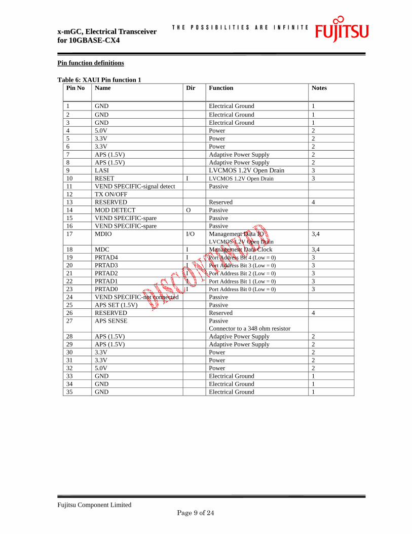
Pin function definitions Table 6: XAUI Pin function 1
Pin No Name
Dir
Function
Notes
1 GND Electrical Ground 1 2 GND Electrical Ground 1 3 GND Electrical Ground 1 4 5.0V Power 2 5 3.3V Power 2 6 3.3V Power 2 7 APS (1.5V) Adaptive Power Supply 2 8 APS (1.5V) Adaptive Power Supply 2 9 LASI LVCMOS 1.2V Open Drain 3 10 RESET I LVCMOS 1.2V Open Drain 3 11 VEND SPECIFIC-signal detect Passive 12 TX ON/OFF 13 RESERVED Reserved 4 14 MOD DETECT O Passive 15 VEND SPECIFIC-spare Passive 16 VEND SPECIFIC-spare Passive 17 MDIO I/O Management Data IO
LVCMOS 1.2V Open Drain 3,4
18 MDC I Management Data Clock 3,4 19 PRTAD4 I Port Address Bit 4 (Low = 0) 3 20 PRTAD3 I Port Address Bit 3 (Low = 0) 3 21 PRTAD2 I Port Address Bit 2 (Low = 0) 3 22 PRTAD1 I Port Address Bit 1 (Low = 0) 3 23 PRTAD0 I Port Address Bit 0 (Low = 0) 3 24 VEND SPECIFIC-not connected Passive 25 APS SET (1.5V) Passive 26 RESERVED Reserved 4 27 APS SENSE Passive
Connector to a 348 ohm resistor
28 APS (1.5V) Adaptive Power Supply 2 29 APS (1.5V) Adaptive Power Supply 2 30 3.3V Power 2 31 3.3V Power 2 32 5.0V Power 2 33 GND Electrical Ground 1 34 GND Electrical Ground 1 35 GND Electrical Ground 1

xx--mmGGCC,, EElleeccttrriiccaall TTrraannsscceeiivveerr ffoorr 1100GGBBAASSEE--CCXX44
Fujitsu Component Limited Page 10 of 24
Table 7: XAUI Pin function 2 Pin No Name
Dir
Function
Notes
36 GND Electrical Ground 1 37 GND Electrical Ground 1 38 RESERVED Reserved 39 RESERVED Reserved 40 GND Electrical Ground 1 41 RX LANE0+ Module XAUI Output Lane 0+ 5 42 RX LANE0- Module XAUI Output Lane 0- 5 43 GND Electrical Ground 1 44 RX LANE1+ Module XAUI Output Lane 1+ 5 45 RX LANE1- Module XAUI Output Lane 1- 5 46 GND Electrical Ground 1 47 RX LANE2+ Module XAUI Output Lane 2+ 5 48 RX LANE2- Module XAUI Output Lane 2- 5 49 GND Electrical Ground 1 50 RX LANE3+ Module XAUI Output Lane 3+ 5 51 RX LANE3- Module XAUI Output Lane 3- 5 52 GND Electrical Ground 1 53 GND Electrical Ground 1 54 GND Electrical Ground 1 55 TX LANE0+ Module XAUI Input Lane 0+ 5 56 TX LANE0- Module XAUI Input Lane 0- 5 57 GND Electrical Ground 1 58 TX LANE1+ Module XAUI Input Lane 1+ 5 59 TX LANE1- Module XAUI Input Lane 1- 5 60 GND Electrical Ground 1 61 TX LANE2+ Module XAUI Input Lane 2+ 5 62 TX LANE2- Module XAUI Input Lane 2- 5 63 GND Electrical Ground 1 64 TX LANE3+ Module XAUI Input Lane 3+ 5 65 TX LANE3- Module XAUI Input Lane 3- 5 66 GND Electrical Ground 1 67 RESERVED Reserved 68 RESERVED Reserved 69 GND Electrical Ground 1 70 GND Electrical Ground 1
Notes: 1) Ground connections are common for TX and RX. 2) All contacts of XAUI 70 pin connector are rated at 0.5A nominal. 3) 1.2V CMOS compatible. 4) MDIO and MDC timing must comply with IEEE802.3ae, Clause 45.3 5) XAUI output characteristics should comply with IEEE802.3ae Clause 47.

xx--mmGGCC,, EElleeccttrriiccaall TTrraannsscceeiivveerr ffoorr 1100GGBBAASSEE--CCXX44
Fujitsu Component Limited Page 11 of 24
Package Design
Mechanical design of x-mGC is shown as in following figure8.
Figure 8: Mechanical Design
(Part Number: FCU-022M101) Note2)This module is unable to withstand aqueous wash Note1) Unless otherwise specified, tolerance shall be +/-0.5mm.
Datum B is physical hard stop for transceiver. Datum D is vertical center of transceiver PCB. Datum E is top surface of rail slot on transceiver. Datum F is front surface of customers faceplate.

xx--mmGGCC,, EElleeccttrriiccaall TTrraannsscceeiivveerr ffoorr 1100GGBBAASSEE--CCXX44
Fujitsu Component Limited Page 12 of 24
APPENDIX A : Programmable Logic Implementation 1 SCOPE This document scopes to x-mGC (XENPAK/X2-CX4), P/N :FCU-010M002-** (XENPAK), FCU-02*M101-** (X2) 2 INTRODUCTION
This document describes management block implementation when x-mGC is used as 10G-CX4 PHY transceiver in
XENPAK/X2-type application.
Figure 1 describes the generic x-mGC design block diagram using retimer IC.
• High speed block includes a retimer IC 10G CX4-compliant device which ensures full-duplex
XAUI-to-CX4 communication link
• Power block that includes adaptive power supply support and Power filtering
• The management block includes a register file that host can access. a non volatile memory (NVR) stores the
default value of this register file. The host reads the register file for system capabilities, vendor information
and link status information.
The host may read or write from the register file, store its content in the NVR or load the default value from
the NVR.
Retimer
CX4 connector
XENPAK/X2 host Interface
Managment Block
NVR NVRinterface
Power Supply

xx--mmGGCC,, EElleeccttrriiccaall TTrraannsscceeiivveerr ffoorr 1100GGBBAASSEE--CCXX44
Fujitsu Component Limited Page 13 of 24
The host may indirectly access the link and host transceivers to change setting or to read status information.
Following reset or power up the management block initializes the host and link transceiver by a pre defined
initialization sequence. After the initialization the management reads a defined link of link status registers
and stores them in the register file. In case of a link status event the management generates an interrupt
signal name Link Alarm Status Interrupt (LASI).
3. Functional description The Management block in the retimer IC XENPAK/X2-RD is implemented in a FPGA. The The FPGA is updated
over JTAG. The code is written to be ported to any other technology with minimal usage of technology specific
macro. Any macro that can not be avoided is set to a specific verilog file.
Features
• Compliant with XENPAK MSA 3.0 / X2 MSA 2.0
• SMI (MDIO/MDC) – 802.3ae compliant
• I2C I/O – to upload EPROM content (Vendor Specific Info)
• Link Alarm Status Interrupt (LASI) support.
• Non volatile memory that contains XENPAK/X2 registers default value.
• In Circuit programming for FPGA over JTAG
• XENPAK/X2 registers file mapped to Host MDIO space with configurable port address.
• Retimer IC initialization
• Retimer IC performance optimization routine (optional)
• Signal detect indication

xx--mmGGCC,, EElleeccttrriiccaall TTrraannsscceeiivveerr ffoorr 1100GGBBAASSEE--CCXX44
Fujitsu Component Limited Page 14 of 24
Internal architecture The following figure describes internal FPGA functionality:
Xenpack registers
NVR acess FSM
SMI Target
XEN Reg wr
Xen reg rd
NVR commands
NVR command status
NVR writeNVR readNVR wr data
NVR add
LASILASI control
LASI status
SMI masterSMI masterFSM
PHY ini data(ROM)
PHY reg.addPHYreg.wrdataPHY addressPHYreg.wrPHYreg.rd
PHYini.address PHYin.data
PHYreg.rddata
LASI status registersupdate
LASI block
MDC
MDI
MDO
MDOOE
MDC
MDOOE
MDI
MDO
eeprom interface
External serial EEPORM
NVR rd data
EECLKEEDO EEDI EECS
SMI control by host
XM_SMI
PHY reg.addPHYreg.wrdataPHY addressPHYreg.wrPHYreg.rd
PHYreg.rddata
HOST SMI
Figure 1 FPGA block diagram
The management block is comprised of several sub blocks.
A XENPAK/X2 register file is a volatile memory that is mapped to the host MDIO address space. The
XENPAK/X2 register file is defined by the XENPAK/X2 MSA. It makes use of the lower eight bit of the MDIO
data register. (Except from the host indirect SMI access registers)
The host may read or write each register from the XENPAK/X2 register file. It can load or save the whole
register file in a Non Volatile memory.
The XENPAK/X2 register file is mapped into device number 2, at the port address set by the host.
The Non Volatile RAM (NVR) FSM, manages NVR access.
The following NVR commands are supported:
Write all
Read all
In case of read/write all the state machine manages address incrementing and data transfer from register file
to NVR.
NVR master, performs a 2 wire NVR commands as described by the EEPROM vendor, this is a separate module
support of other NVR devices is done by replacing this module.
Link Alarm Status Interrupt (LASI) circuit. Generates an interrupt if one of the events in the following table
occurs (set). The user may mask each one of the events. The LASI block implementation follows figure 21 in

xx--mmGGCC,, EElleeccttrriiccaall TTrraannsscceeiivveerr ffoorr 1100GGBBAASSEE--CCXX44
Fujitsu Component Limited Page 15 of 24
the MSA. With the following exceptions:
Global PMD signal PK is not applicable
PCS block lock 1 is not applicable.
WIS Local fault not applicable
Laser Fault not applicable
Initialization ROM data is a ROM that stores the initialization date.
SMI master together read writes the transceivers register files. In initialize the transceivers after power up and
reset and reads the status registers used by the LASI block.
The following state machine describes the SMI master state machine.
fetch data from inidata ROM
state 0ROMFERCH
Finished ini sequence(rid_last =1)
SMI initalizationwrite
state 1
read reg 1.10.0state 2
read reg 3.32.0state 3
read reg 4.24.12state 4
read reg 1.8.10state 5
read reg 3.8.10state 6
read reg 4.8.10state 7
Pol reg 1.8.11state 9
Pol reg 3.8.11state 10
Pol reg 4.8.11state 11
RESET/POWER UP
data is transfered fromRID to SMIM, generatestart pulse, latch ROMdata on exist from state
increase ROM addressWait till SMI tranaction
finsh wait for ready fromSMI master
Data from ROM is beingtrasfered via a trasparentlatch that is open duriong
this state
set the address/datagenerate start pulse
wait to ready
set the address/datagenerate start pulse
wait to ready
HOST controlstate 12
To IndirectMDIOaccessFSM

xx--mmGGCC,, EElleeccttrriiccaall TTrraannsscceeiivveerr ffoorr 1100GGBBAASSEE--CCXX44
Fujitsu Component Limited Page 16 of 24
Interface Host interface Signal Name Type Direction Description MDC HSTL I Host Management clock MDI HSTL I Host Management Data Input MDO LVCMOS
OD O Host Management Data Output
XENP_PRTAD [4:0]
HSTL I Xenpak/X2 registers Port Address
TX_ON_OFF HSTL I Transmit on off (only apply for optical module)
LASI_OUT LVCMOSOD
O Link Alarm Status Interrupt output
VSPEC[3:1] LVCMOS O Vendor specific [3:1]
PHY interface Signal Name Type Direction Description XM_MDC HSTL O Xenpak/X2 module management clock
output, toggling at XM_CLK /8 XM_MDO LVCMOS
OD O Xenpak/X2 module management data output
XM_MDI HSTL I Xenpak/X2 module management input XM_RST_N LVCMOS
OD O Xenpak/X2 module active low reset output
D1_LED_TX0 HSTL I Signal detect from port1 D2_LED_TX0 HSTL I Signal detect from port2 RMTCTRL HSTL O Remote control
EEPROM interface Signal Name Type Direction Description SDA LVCMOS IO EEPROM data SCL LVCMOS O EEPROM clock WP LVCMOS O EEPROM Write protect
Global Signal Name Type Direction Description XM_CLK
LVCOMS I Clock input 20Mhz
HRST_N LVCMOS I Hardware Active Low reset Input

xx--mmGGCC,, EElleeccttrriiccaall TTrraannsscceeiivveerr ffoorr 1100GGBBAASSEE--CCXX44
Fujitsu Component Limited Page 17 of 24
Programming interface Port and device mapping
The XENPAK/X2 module is mapped to the host MDIO address space. The host accesses the module using SMI
transactions. SMI frame description appeared in Table 45-64 in the IEEE 802.3ea standard.
• The Host sets the XENPAK/X2 module port address. The XENPAK/X2 register file is
mapped to device 2 at that port address.
• The XENPAK/X2 module as an internal SMI bus that enable the management block to
access the retimer registers this bus is S_SMI. In this bus the line transceiver is at port
address 1 and the host transceiver is at port address 2. The registers in the retimer are
mapped to devices 4.
• The host has indirect access to the retimer via registers mapped to the XENPAK/X2 vendor specific space. The XENPAK/X2 module has an internal SMI secondary bus. On that bus, port one is mapped to SMI port address “2” while port two is mapped to SMI port address “3”.
Register Map
Register Address
Register Name Default value
32768 NVR control/Status Refer to page 23 32775 Version A 32776 NVR_size 0 1 32777 NVR_size 1 0 32778 Mem_Used 1 32779 Mem_Used 0 32780 Basic Addr B 32781 Cust Adde 77 32782 Vend Addr A7 32783 Ext Vend Addr 0 1 32784 Ext Vend Addr 1 0 32785 reserved 0 32786 Tcvr Type 1: XENPAK, 2: X2 32787 Connector 0 32788 Encoding 1 32789 Bit rate H 27 32790 Bit rate L 10 32791 Protocol 1 32792 Std comp Code 0 0 32793 Std comp Code 1 0 32794 Std comp Code 2 0 32795 Std comp Code 3 0 32796 Std comp Code 4 0 32797 Std comp Code 5 0 32798 Std comp Code 6 0 32799 Std comp Code 7 0 32800 Std comp Code 8 0

xx--mmGGCC,, EElleeccttrriiccaall TTrraannsscceeiivveerr ffoorr 1100GGBBAASSEE--CCXX44
Fujitsu Component Limited Page 18 of 24
Register Address
Register Name Default value
32801 Std comp Code 9 0 32802 Range 0 0 32803 Range 1 0 32804 Fiber type 0 0 32805 Fiber type 1 0 32806 Wave Length ch. 00 0 32807 Wave Length ch. 01 0 32808 Wave Length ch. 02 0 32809 Wave Length ch. 10 0 32810 Wave Length ch. 11 0 32811 Wave Length ch. 12 0 32812 Wave Length ch. 20 0 32813 Wave Length ch. 21 0 32814 Wave Length ch. 22 0 32815 Wave Length ch. 30 0 32816 Wave Length ch. 31 0 32817 Wave Length ch. 32 0 32818 Package OUI 0 0 32819 Package OUI 1 41:XENPAK, C0:X2 32820 Package OUI 2 F4:XENPAK, 98:X2 32821 Package OUI 3 0 32822 Vendor OUI 0 0 32823 Vendor OUI 1 9 32824 Vendor OUI 2 2 32825 Vendor OUI 3 2 32826 Vendor Name 0 46 32827 Vendor Name 1 75 32828 Vendor Name 2 6A 32829 Vendor Name 3 69 32830 Vendor Name 4 74 32831 Vendor Name 5 73 32832 Vendor Name 6 75 32833 Vendor Name 7 43 32834 Vendor Name 8 6F 32835 Vendor Name 9 6D 32836 Vendor Name 10 70 32837 Vendor Name 11 6F 32838 Vendor Name 12 6E 32839 Vendor Name 13 65 32840 Vendor Name 14 6E 32841 Vendor Name 15 74 32842 Vendor P/N 0 46 32843 Vendor P/N 1 43 32844 Vendor P/N 2 55 32845 Vendor P/N 3 2D 32846 Vendor P/N 4 30 32847 Vendor P/N 5 31:XENPAK, 32:X2 32848 Vendor P/N 6 30:XENPAK, 32:X2 32849 Vendor P/N 7 4D 32850 Vendor P/N 8 30:XENPAK, 31:X2 32851 Vendor P/N 9 30

xx--mmGGCC,, EElleeccttrriiccaall TTrraannsscceeiivveerr ffoorr 1100GGBBAASSEE--CCXX44
Fujitsu Component Limited Page 19 of 24
Register Address
Register Name Default value
32852 Vendor P/N 10 32:XENPAK, 31:X2 32853 Vendor P/N 11 20 32854 Vendor P/N 12 20 32855 Vendor P/N 13 20 32856 Vendor P/N 14 20 32857 Vendor P/N 15 20 32858 Vendor Rev 0 Vender information 32859 Vendor Rev 1 Vender information 32860 Vendor SN 0 0 32861 Vendor SN 1 0 32862 Vendor SN 2 0 32863 Vendor SN 3 0 32864 Vendor SN 4 0 32865 Vendor SN 5 0 32866 Vendor SN 6 0 32867 Vendor SN 7 0 32868 Vendor SN 8 0 32869 Vendor SN 9 0 32870 Vendor SN 10 0 32871 Vendor SN 11 0 32872 Vendor SN 12 0 32873 Vendor SN 13 0 32874 Vendor SN 14 0 32875 Vendor SN 15 0 32876 Data code Year 0 Vender information 32877 Data code Year 1 Vender information 32878 Data code Year 2 Vender information 32879 Data code Year 3 Vender information 32880 Date Code Month 0 Vender information 32881 Date Code Month 1 Vender information 32882 Date Code Day 0 Vender information 32883 Date Code Day 1 Vender information 32884 Date Code Lot 0 Vender information 32885 Date Code Lot 1 Vender information 32886 Current ref 5v 0 32887 Current ref 3.3v 4 32888 Current ref APS Stress 4 32889 APS voltage 10 32890 DOM cap 0 32891 Optional Cap 0 32892 reserved 0 32893 Basic Check sum 0 32894 Customer Area 0 0 32895 Customer Area 1 0 32896 Customer Area 2 0 32897 Customer Area 3 0 32898 Customer Area 4 0 32899 Customer Area 5 0 32900 Customer Area 6 0 32901 Customer Area 7 0 32902 Customer Area 8 0

xx--mmGGCC,, EElleeccttrriiccaall TTrraannsscceeiivveerr ffoorr 1100GGBBAASSEE--CCXX44
Fujitsu Component Limited Page 20 of 24
Register Address
Register Name Default value
32903 Customer Area 9 0 32904 Customer Area 10 0 32905 Customer Area 11 0 32906 Customer Area 12 0 32907 Customer Area 13 0 32908 Customer Area 14 0 32909 Customer Area 15 0 32910 Customer Area 16 0 32911 Customer Area 17 0 32912 Customer Area 18 0 32913 Customer Area 19 0 32914 Customer Area 20 0 32915 Customer Area 21 0 32916 Customer Area 22 0 32917 Customer Area 23 0 32918 Customer Area 24 0 32919 Customer Area 25 0 32920 Customer Area 26 0 32921 Customer Area 27 0 32922 Customer Area 28 0 32923 Customer Area 29 0 32924 Customer Area 30 0 32925 Customer Area 31 0 32926 Customer Area 32 0 32927 Customer Area 33 0 32928 Customer Area 34 0 32929 Customer Area 35 0 32930 Customer Area 36 0 32931 Customer Area 37 0 32932 Customer Area 38 0 32933 Customer Area 39 0 32934 Customer Area 40 0 32935 Customer Area 41 0 32936 Customer Area 42 0 32937 Customer Area 43 0 32938 Customer Area 44 0 32939 Customer Area 45 0 32940 Customer Area 46 0 32941 Customer Area 47 0 32942 XM_SMI Register address Refer to page 23 32943 XM_SMI Register data Refer to page 23 32944 XM_SMI command Refer to page 23 32945 AGGREGATE_MOD_CTRL Refer to page 24 32946 - 33030 Vender Specific 0 36864 RX_ALARM_CTRL Refer to page 24 36865 TX_ALARM_CTRL Refer to page 24 36866 LASI_CTRL Refer to page 25 36867 RX_ALARM_STAT Refer to page 25 36868 TX_ALARM_STAT Refer to page 25 36869 LASI_STAT Refer to page 26

xx--mmGGCC,, EElleeccttrriiccaall TTrraannsscceeiivveerr ffoorr 1100GGBBAASSEE--CCXX44
Fujitsu Component Limited Page 21 of 24
Register detailed description
Register 0x8000 -- NVR_CTRL_STAT Address Name Description Mode Default 0.15:6 Reserved NO
0.5 COMM Command 0 = Read NVR 1 = Write NVR The set this bit to perform write operation or clear it for read operation
RW 0
0.4 Reserved NO 0.3:2 COMM_STAT command status
00 = Idle 01 = Command completed successfully 10 = Command in progress 11 = Command failed
RO 00
0.1:0 EXT_COMM Extended command 00 = Reserved 01 = Reserved 10 = Reserved 11 = Read/Write all NVR Writing 11 to this filed performs write or read operation
to/from all registers depends on the value of command field.
RW 11
Register 0x80AE -- XM_SMI_ADDR Address Name Description Mode Default 174.15:0 XM_SMI_ADDR Address register for HOST indirect SMI transactions RW 0h
Register 0x80AF -- XM_SMI_DATA Address Name Description Mode Default 175.15:0 XM_SMI_DATA Data register for HOST indirect SMI transactions RW 0h
Register 0x80B0 -- XM_SMI_COMMAND Address Name Description Mode Default 176.15:3 Reserved NO
176.2 WR_COMMAND Specifies the host initiate SMI write transaction. This register is cleared at the end of the write operation 0 = idle 1 = write command
RW 0
176.1 RD_COMMAND Specifies the host initiate SMI read transaction This register is cleared at the end of the write operation 0 = idle 1 = read operation Notice: a write operation has priority over read operation.
RW 0
176.0 HOST_LINE Specifies to which PHY the host turns 0 = host turns to line phy 1 = host turns to host phy
RW 0

xx--mmGGCC,, EElleeccttrriiccaall TTrraannsscceeiivveerr ffoorr 1100GGBBAASSEE--CCXX44
Fujitsu Component Limited Page 22 of 24
Register 0x80B1 -- AGGREGATE_MOD_CTRL Address Name Description Mode Default
7:4 Reserved NO 3 XMRESET The content of this register drives xmreset
0 – Normal operation 1 – Retimer is held at reset
RW 0
2 write_protect This register write protecting the basic region and vendor specific register 0 = vendor specific register area is not write protected 1 = vendor specific is write protected
RW 1
1 D2_INT_AGG The content of this register drives INT/AGG input of the retimer port 2
RW 1
0 D1_INT_AGG The content of this register drives INT/AGG input of the retimer port 1
RW 1
Register 0x9000 -- RX_ALARM_CTRL
Address Name Description Mode Default 0.15:5 Reserved NO
0.4 PMA_PMD_REC_LOC_FAULT_CT
RL
PMA/PMD local receiver fault control, setting this bit enables LASI indication for PMA/PMD local receiver fault. 0 – Disable 1 - Enable
RW 1
0.3 PCS_REC_LOC_FAULT_CTRL
PCS local receiver fault control, setting this bit enables LASI indication for PCS local receiver fault. 0 – Disable 1 - Enable
RW 1
0.2:1 Reserved NO 0.0 PHY_XS_REC_L
OC_FAULT_CTRL
PHY XS local receiver fault control, setting this bit enables LASI indication for PHY XS local receiver fault. 0 – Disable 1 - Enable
RW 1
Register 0x9001 -- TX_ALARM_CTRL Address Name Description Mode Default
15:5 Reserved NO 4 PMA_PMD_TAR_
LOC_FAULT_CTRL
PMA/PMD local transmitter fault control, setting this bit enables LASI indication for PMA/PMD local transmitter fault. 0 – Disable 1 - Enable
RW 1
3 PCS_TAR_LOC_FAULT_CTRL
PCS local transmitter fault control, setting this bit enables LASI indication for PCS local transmitter fault. 0 – Disable 1 - Enable
RW 1
2:1 Reserved NO

xx--mmGGCC,, EElleeccttrriiccaall TTrraannsscceeiivveerr ffoorr 1100GGBBAASSEE--CCXX44
Fujitsu Component Limited Page 23 of 24
Address Name Description Mode Default 0 PHY_XS_TAR_L
OC_FAULT_CTRL
PHY XS local transmitter fault control, setting this bit enables LASI indication for PHY XS local transmitter fault. 0 – Disable 1 - Enable
RW 1
Register 0x9002 -- LASI_CTRL Address Name Description Mode Default
15:3 Reserved NO 2 RX_ALARM_EN receive alarm enable
0 – disable 1 – Enable
RW 0
1 TX_ALARM_EN Transmit alarm enable 0 – disable 1 – enable
RW 0
0 LS_ALARM_EN LASI alarm enable 0 – disable 1 – enable
RW 0
Register 0x9003 -- RX_ALARM_STAT Address Name Description Mode Default
15:5 Reserved NO 4 PMA_PMD_REC_
LOC_FAULT_STAT
PMA/PMD local receiver fault status, 0 – Normal 1 – Fault indication
RO 0
3 PCS_REC_LOC_FAULT_STAT
PCS local receiver fault status, 0 – Normal 1 – Fault indication
RO 0
2:1 Reserved NO 0 PHY_XS_REC_L
OC_FAULT_STAT PHY XS local receiver fault status, 0 – Normal 1 – Fault indication
RO 0
Register 0x9004 -- TX_ALARM_STAT Address Name Description Mode Default
15:5 Reserved NO 4 PMA_PMD_TAR_
LOC_FAULT_STAT
PMA/PMD local transmitter fault status, 0 – Normal 1 – Fault indication
RO 0
3 PCS_TAR_LOC_FAULT_STAT
PCS local transmitter fault status, 0 – Normal 1 – Fault indication
RO 0
2:1 Reserved NO 0 PHY_XS_TAR_L
OC_FAULT_STAT PHY XS local transmitter fault status, 0 – Normal 1 – Fault indication
RO 0

xx--mmGGCC,, EElleeccttrriiccaall TTrraannsscceeiivveerr ffoorr 1100GGBBAASSEE--CCXX44
Fujitsu Component Limited Page 24 of 24
Register 0x9005 -- LASI_STAT Address Name Description Mode Default
15:4 Reserved NO 3 SMI_MFSM_HOS
T_CONTROL_GRANT
RO 0
2 RX_ALARM Receive alarm status RO 0 1 TX_ALARM Transmit alarm status RO 0 0 LS_ALARM LASI alarm status RO 0
References • XENPAK 10 Gigabit Ethernet MSA rev 3.0, X2 10 Gigabit Ethernet MSA rev 2.0
• IEEE 802.3ae clause 45