www.tyndall.ie 1 semiconductor processing lecture 1- resists, lithography and mask design dr. james...
TRANSCRIPT
www.tyndall.ie1
Semiconductor processing
Lecture 1- Resists, lithography and
mask design
Dr. James R O’Callaghan
23rd September 2013
www.tyndall.ie2
Processing
• The simplest form of a semiconductor device is a PN junction i.e. a diode.
• However, how do you turn a p and n type semiconductor into an actual device?
• The technologies involved are all intertwined but can be separated into resists, lithography, thin film deposition and etching. These allow us to form the structures the create the actual physical device.
www.tyndall.ie3
Lithography
• Lithography from Greek λίθος - lithos, 'stone' + γράφειν - graphein, 'to write‘.
• Is a process of transferring information onto a substrate so that the substrate’s nature can be changed.
• The predefined pattern is referred to as a mask and is usually defined in terms of transmission of an activating light source onto a responsive polymer on the surface of the substrate.
www.tyndall.ie4
The basics
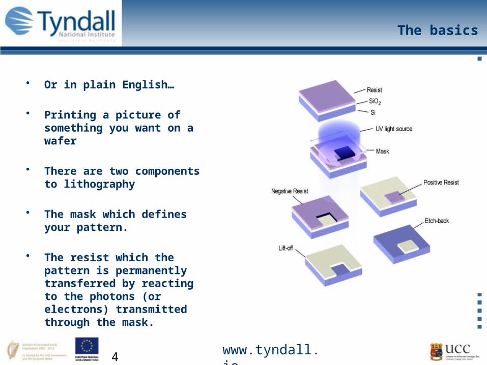
• Or in plain English…
• Printing a picture of something you want on a wafer
• There are two components to lithography
• The mask which defines your pattern.
• The resist which the pattern is permanently transferred by reacting to the photons (or electrons) transmitted through the mask.
www.tyndall.ie5
The basics
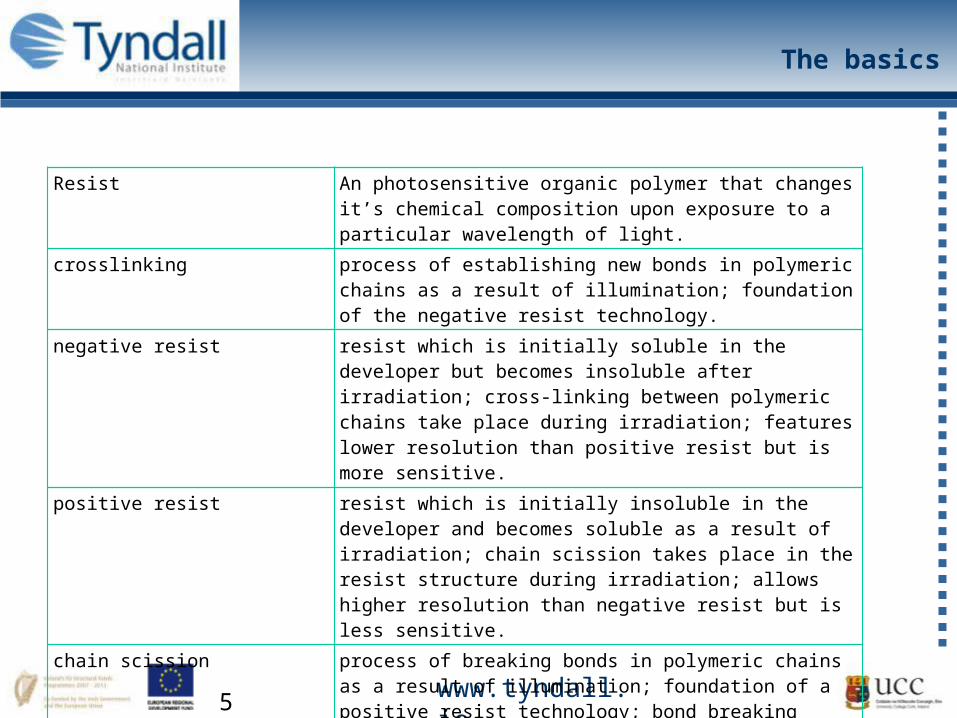
Resist An photosensitive organic polymer that changes it’s chemical composition upon exposure to a particular wavelength of light.
crosslinking process of establishing new bonds in polymeric chains as a result of illumination; foundation of the negative resist technology.
negative resist resist which is initially soluble in the developer but becomes insoluble after irradiation; cross-linking between polymeric chains take place during irradiation; features lower resolution than positive resist but is more sensitive.
positive resist resist which is initially insoluble in the developer and becomes soluble as a result of irradiation; chain scission takes place in the resist structure during irradiation; allows higher resolution than negative resist but is less sensitive.
chain scission process of breaking bonds in polymeric chains as a result of illumination; foundation of a positive resist technology; bond breaking makes positive resist soluble in the developer.
www.tyndall.ie6
Resist deposition
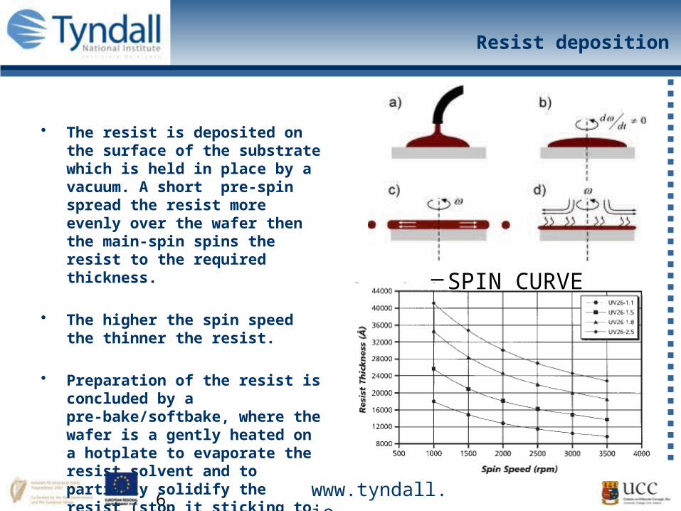
• The resist is deposited on the surface of the substrate which is held in place by a vacuum. A short pre-spin spread the resist more evenly over the wafer then the main-spin spins the resist to the required thickness.
• The higher the spin speed the thinner the resist.
• Preparation of the resist is concluded by a pre-bake/softbake, where the wafer is a gently heated on a hotplate to evaporate the resist solvent and to partially solidify the resist (stop it sticking to the mask).
–SPIN CURVE
www.tyndall.ie7
Resolution
Depends on 3 main factors
1. Wavelength of the system: The shorter the wavelength the smaller the feature size. This is because lower wavelengths suffer from diffraction less and can be focused to a smaller spot size (in the case of direct write i.e. e-beam) or diffract less from the edge of the mask features. UV (365nm) – typical feature size ~ 0.5µm DUV(248nm) ~ 0.3µm e-beam <100nm.
2. The system employed: Contact, proximity, stepper, direct write. How good are it’s optics? The closeness of the mask to the resist etc.
3. The resist: The thinner the resist the sharper your image. However, the thinner your resist the less masking you achieve i.e. thin resist sharp image but useless for deep etching as the resist will have ablated during the process. There are ways around this but it all depends on your process and its limitations
www.tyndall.ie8
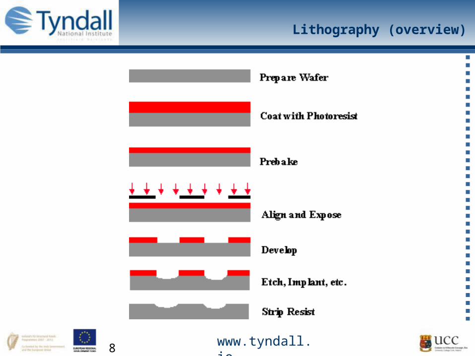
Lithography (overview)
www.tyndall.ie9
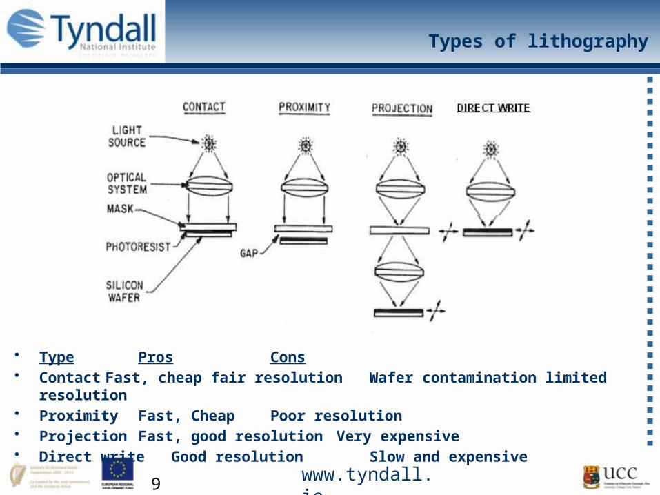
Types of lithography
• Type Pros Cons• ContactFast, cheap fair resolution Wafer contamination limited
resolution• Proximity Fast, Cheap Poor resolution• Projection Fast, good resolution Very expensive• Direct write Good resolution Slow and expensive
www.tyndall.ie10
Imprint lithography
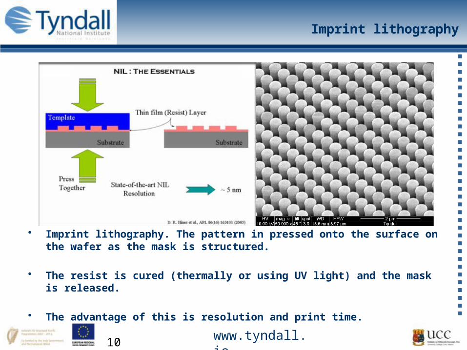
• Imprint lithography. The pattern in pressed onto the surface on the wafer as the mask is structured.
• The resist is cured (thermally or using UV light) and the mask is released.
• The advantage of this is resolution and print time.
www.tyndall.ie11
The Mask aligner
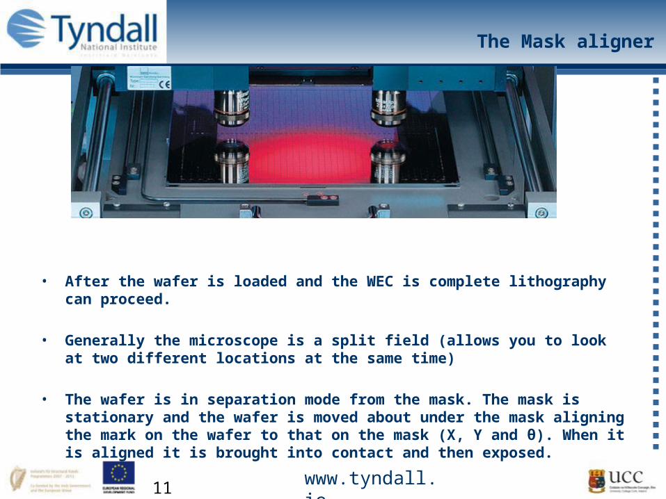
• After the wafer is loaded and the WEC is complete lithography can proceed.
• Generally the microscope is a split field (allows you to look at two different locations at the same time)
• The wafer is in separation mode from the mask. The mask is stationary and the wafer is moved about under the mask aligning the mark on the wafer to that on the mask (X, Y and θ). When it is aligned it is brought into contact and then exposed.
www.tyndall.ie12
The Mask Aligner 2
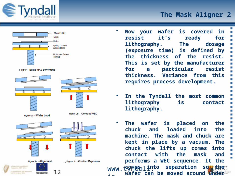
• Now your wafer is covered in resist it’s ready for lithography. The dosage (exposure time) is defined by the thickness of the resist. This is set by the manufacturer for a particular resist thickness. Variance from this requires process development.
• In the Tyndall the most common lithography is contact lithography.
• The wafer is placed on the chuck and loaded into the machine. The mask and chuck are kept in place by a vacuum. The chuck the lifts up comes into contact with the mask and performs a WEC sequence. It the comes into separation so the wafer can be moved around under the mask.
www.tyndall.ie13
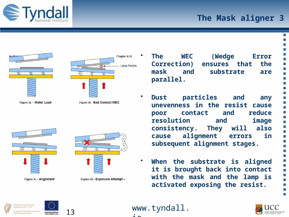
The Mask aligner 3
• The WEC (Wedge Error Correction) ensures that the mask and substrate are parallel.
• Dust particles and any unevenness in the resist cause poor contact and reduce resolution and image consistency. They will also cause alignment errors in subsequent alignment stages.
• When the substrate is aligned it is brought back into contact with the mask and the lamp is activated exposing the resist.
www.tyndall.ie14
Contact modes
Proximity:The wafer is not in contact with the mask. The space between the wafer and mask can be adjusted by through setting the exposure gap parameter.
Soft Contact:The chuck vacuum holds the substrate during exposure, leaving an air gap between the mask and substrate. This mode results in lower resolution compared to other exposure modes but less damage to the mask.
Hard Contact:The vacuum holding the substrate to the chuck is switched off and positive nitrogen pressure is used to press the substrate against the mask. This mode results in better resolution than soft contact but with potential mask damage.
Low Vacuum Contact:Partial vacuum is introduced into the space between the wafer and mask. This causes less wear to the wafer and mask than vacuum contact mode.
Vacuum Contact:A vacuum is drawn between the mask and the substrate during exposure, which brings the wafer in very tight contact with the mask and results in the highest resolution
www.tyndall.ie15
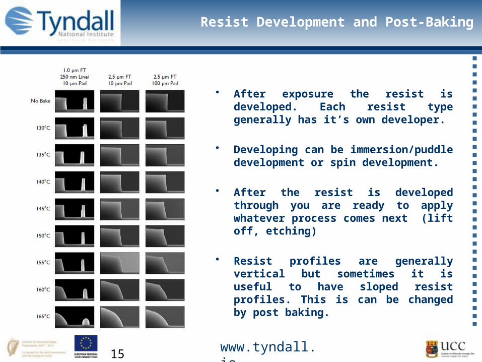
Resist Development and Post-Baking
• After exposure the resist is developed. Each resist type generally has it’s own developer.
• Developing can be immersion/puddle development or spin development.
• After the resist is developed through you are ready to apply whatever process comes next (lift off, etching)
• Resist profiles are generally vertical but sometimes it is useful to have sloped resist profiles. This is can be changed by post baking.
www.tyndall.ie16
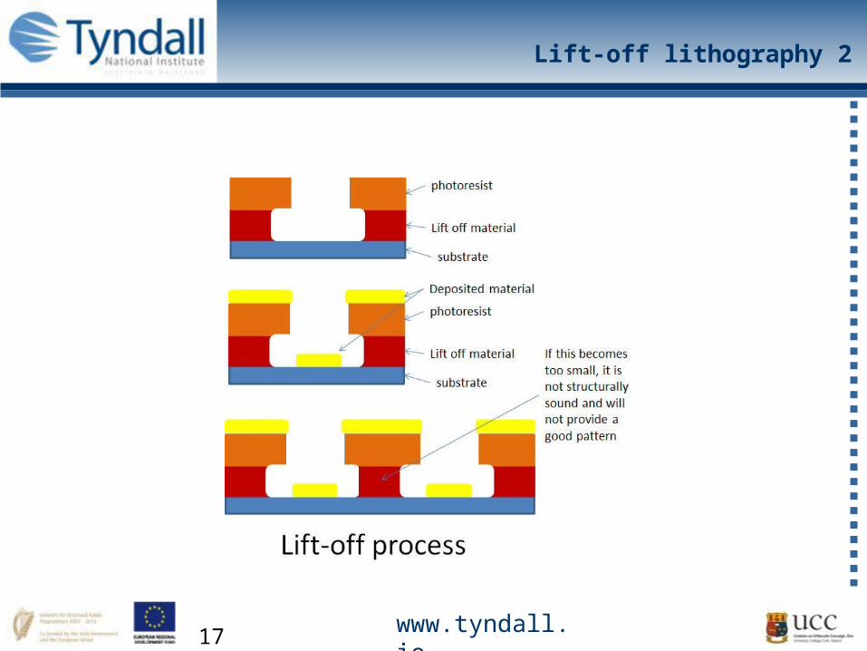
Lift Off lithography 1
• The liftoff process is so that you can deposit a thin film on the surface an the selectively remove it later without the need for any chemical etching.
• This is most common in the deposition of electrical contacts such as gold or aluminum (we’ll get to thin films in the next lecture)
• The lift off process consists of two resists. A lift off resist which is a pre-exposed resist an a pattern resist.
• Lift off resist is spun on first the then the pattern resist is the spun on and exposed. It is the developed and the pattern resist retains the original mask dimensions and the lift off resist develops down and sideward. This allows a gap to forms under the pattern resist.
• This overhang blocks the film being deposited and allows a solvent to access the resist and remove the thin film that is on the surface of the substrate while remaining in areas in which the resist has been developed away.
• It’s a lot more simple to show you
www.tyndall.ie17
Lift-off lithography 2
www.tyndall.ie18
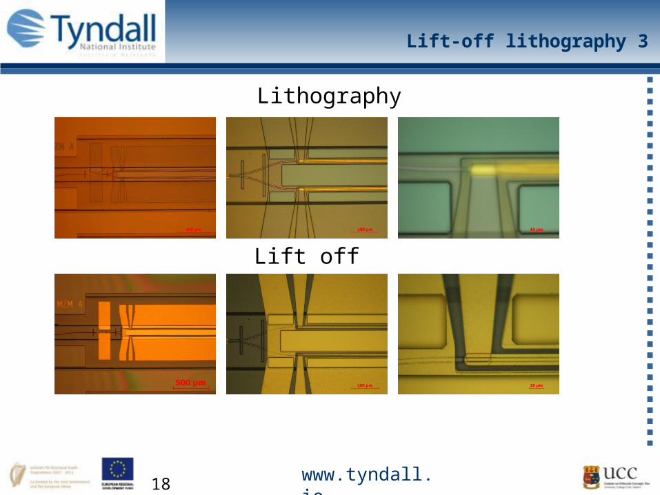
Lift-off lithography 3
Lithography
Lift off
www.tyndall.ie19
Part 2 Mask design and Alignment – Basic guidelines
• Glossary of terms
• Alignment marks
• Design of features
• Circular structures
• Boolean operations
• Mask layout
• Mask order form – parameters and manufacturers
www.tyndall.ie20
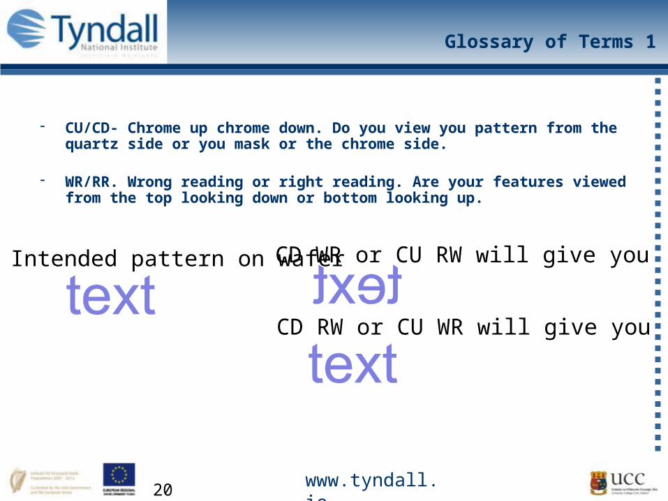
Glossary of Terms 1
- CU/CD- Chrome up chrome down. Do you view you pattern from the quartz side or you mask or the chrome side.
- WR/RR. Wrong reading or right reading. Are your features viewed from the top looking down or bottom looking up.
Intended pattern on wafer CD WR or CU RW will give you
CD RW or CU WR will give you
www.tyndall.ie21
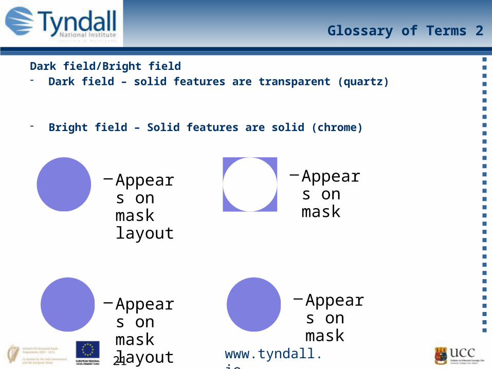
Glossary of Terms 2
Dark field/Bright field- Dark field – solid features are transparent (quartz)
- Bright field – Solid features are solid (chrome)
–Appears on mask layout
–Appears on mask
–Appears on mask layout
–Appears on mask
www.tyndall.ie22
Alignment Marks
• Generally there is more than one lithographic step.
• The first step is the primary
• All subsequent steps must be aligned to this.
• Sometimes your first features can be used to form the alignment marks.
• It is often better to have a separate lithographic section to define alignment marks at the start of processing
www.tyndall.ie23
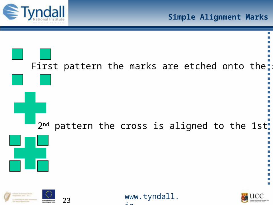
Simple Alignment Marks
First pattern the marks are etched onto the surface
2nd pattern the cross is aligned to the 1st
www.tyndall.ie24
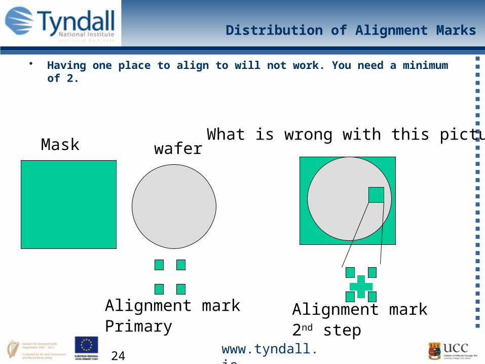
Distribution of Alignment Marks
• Having one place to align to will not work. You need a minimum of 2.
Mask wafer
Alignment mark2nd step
Alignment markPrimary
What is wrong with this picture?
www.tyndall.ie25
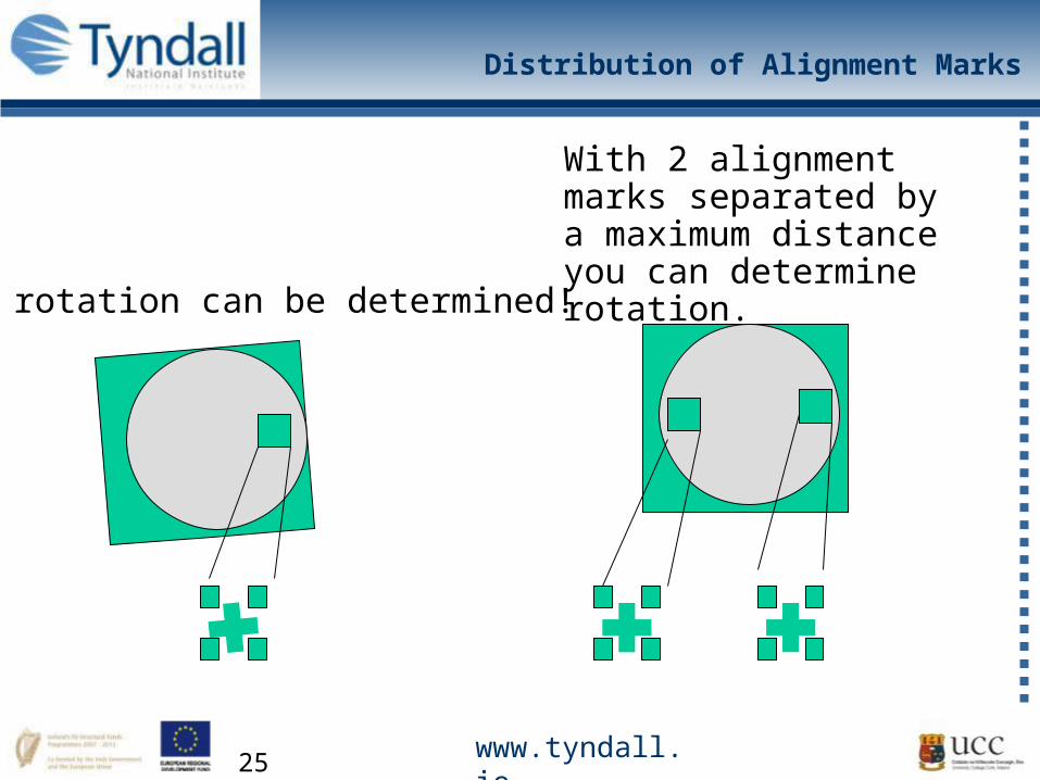
Distribution of Alignment Marks
With 2 alignment marks separated by a maximum distance you can determine rotation.
No rotation can be determined!
www.tyndall.ie26
Polarity of Process 1
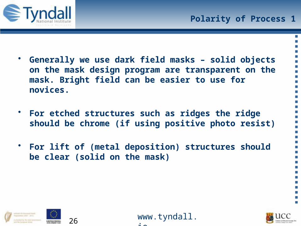
• Generally we use dark field masks – solid objects on the mask design program are transparent on the mask. Bright field can be easier to use for novices.
• For etched structures such as ridges the ridge should be chrome (if using positive photo resist)
• For lift of (metal deposition) structures should be clear (solid on the mask)
www.tyndall.ie27
Polarity of Process 2
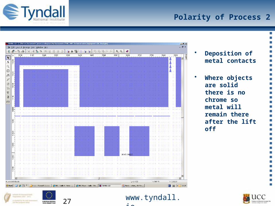
• Deposition of metal contacts
• Where objects are solid there is no chrome so metal will remain there after the lift off
www.tyndall.ie28
Polarity of Process 3
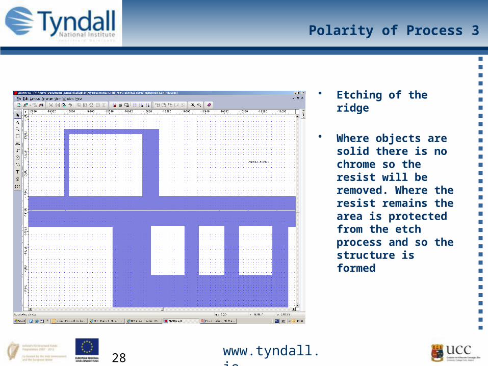
• Etching of the ridge
• Where objects are solid there is no chrome so the resist will be removed. Where the resist remains the area is protected from the etch process and so the structure is formed
www.tyndall.ie29
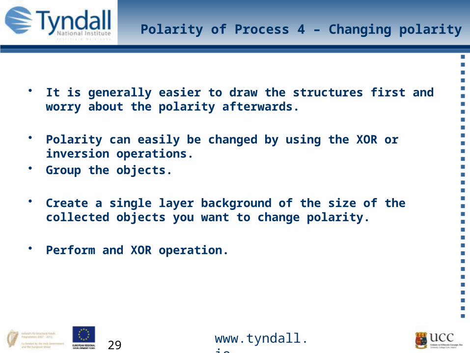
Polarity of Process 4 – Changing polarity
• It is generally easier to draw the structures first and worry about the polarity afterwards.
• Polarity can easily be changed by using the XOR or inversion operations.
• Group the objects.
• Create a single layer background of the size of the collected objects you want to change polarity.
• Perform and XOR operation.
www.tyndall.ie30
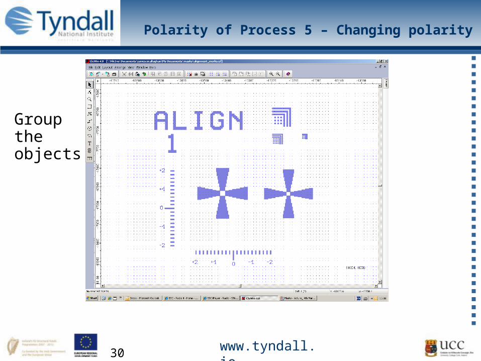
Polarity of Process 5 – Changing polarity
Group the objects
www.tyndall.ie31
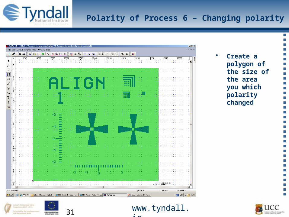
Polarity of Process 6 – Changing polarity
• Create a polygon of the size of the area you which polarity changed
www.tyndall.ie32
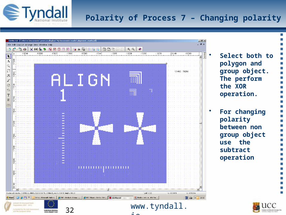
Polarity of Process 7 – Changing polarity
• Select both to polygon and group object. The perform the XOR operation.
• For changing polarity between non group object use the subtract operation
www.tyndall.ie33
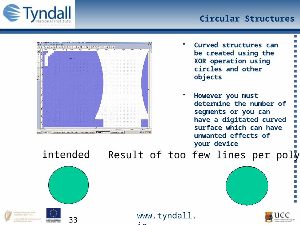
Circular Structures
• Curved structures can be created using the XOR operation using circles and other objects
• However you must determine the number of segments or you can have a digitated curved surface which can have unwanted effects of your device
intended Result of too few lines per polygon

www.tyndall.ie34
Fine Control – Alignment Marks
• For very fine alignment and process quality and monitoring, simple alignment marks will not suffice.
• In this case Vernier alignment marks are necessary
www.tyndall.ie35
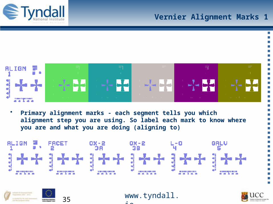
Vernier Alignment Marks 1
• Primary alignment marks - each segment tells you which alignment step you are using. So label each mark to know where you are and what you are doing (aligning to)
www.tyndall.ie36
Vernier Alignment Marks 2
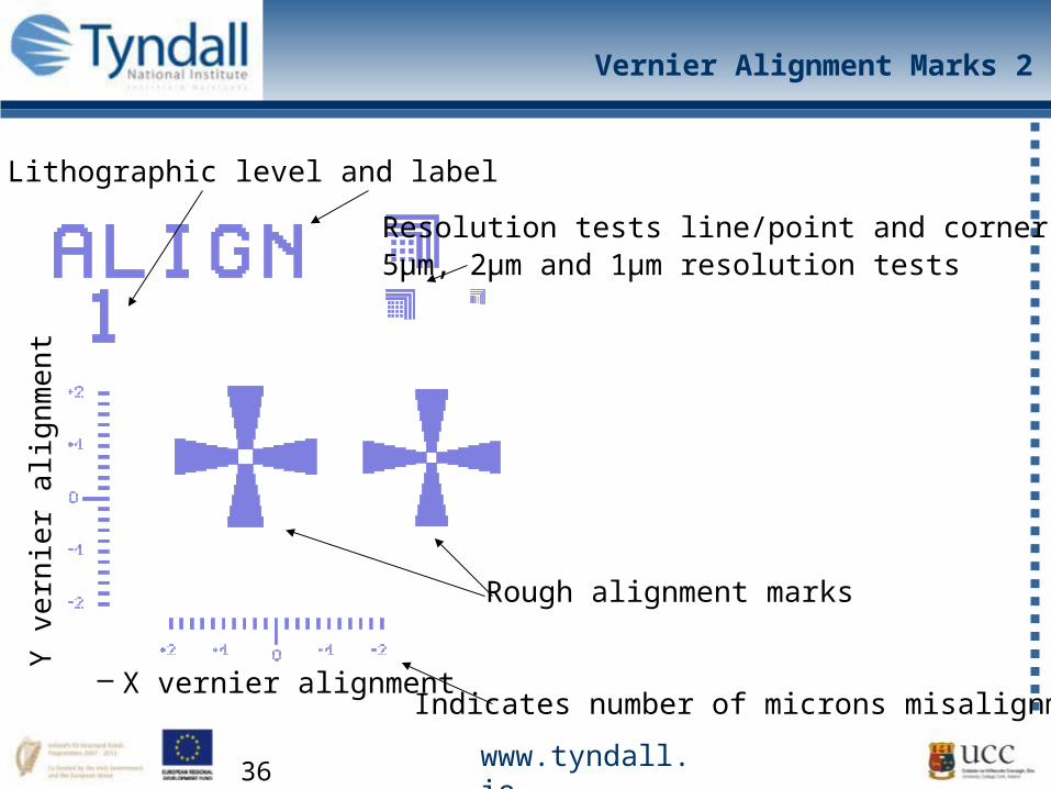
Lithographic level and label
Rough alignment marks
Resolution tests line/point and corner5µm, 2µm and 1µm resolution tests
– X vernier alignment
Y v
erni
er a
lignm
ent
Indicates number of microns misalignment
www.tyndall.ie37
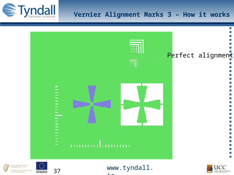
Vernier Alignment Marks 3 – How it works
Perfect alignment
www.tyndall.ie38
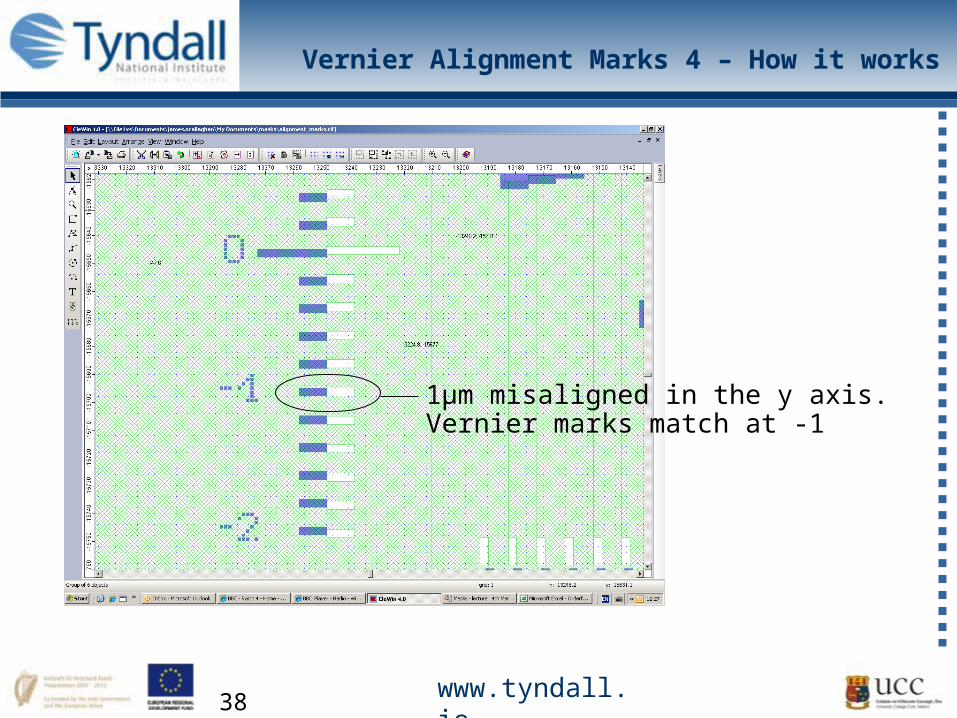
Vernier Alignment Marks 4 – How it works
1µm misaligned in the y axis. Vernier marks match at -1
www.tyndall.ie39
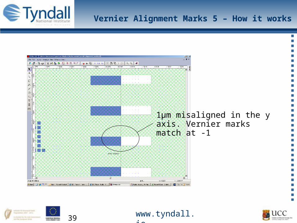
Vernier Alignment Marks 5 – How it works
1µm misaligned in the y axis. Vernier marks match at -1
www.tyndall.ie40
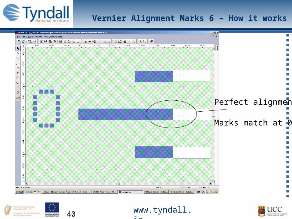
Vernier Alignment Marks 6 – How it works
Perfect alignment
Marks match at 0
www.tyndall.ie41
Alignment summary
1. Load your mask2. Load your wafer with the correct orientation3. Use the rough alignment marks to align first4. Adjust the rotation of the wafer and bring the wafer so that it has
0º misalignment5. Fine adjust the X and Y6. Bring into contact7. If need be bring into separation and readjust8. Bring into contact and run alignment check mode (all conditions of
alignment employed vacuum N2 gas etc.)
9. If everything check out confirm and expose - the lamp will move over the mask and the shutter will open. Don’t look at the lamp unless you want cataracts later in life
www.tyndall.ie42
Summary
• Process first - mask last
• Consult your processor
• Be realistic in terms of resolution and alignment tolerances (don’t try and be a hero).
• The processor must have the final say on the mask. If you are processing yourself for the first time then consult with a grown up.
• The right mask for the right process. E-beam for less than 2µm features LPG for > 2µm
• The smaller the feature size the more expensive the mask.
www.tyndall.ie43
End of Lecture 1
Thanks for listening
Any questions?