wafer bonding technology for hb-led...
TRANSCRIPT
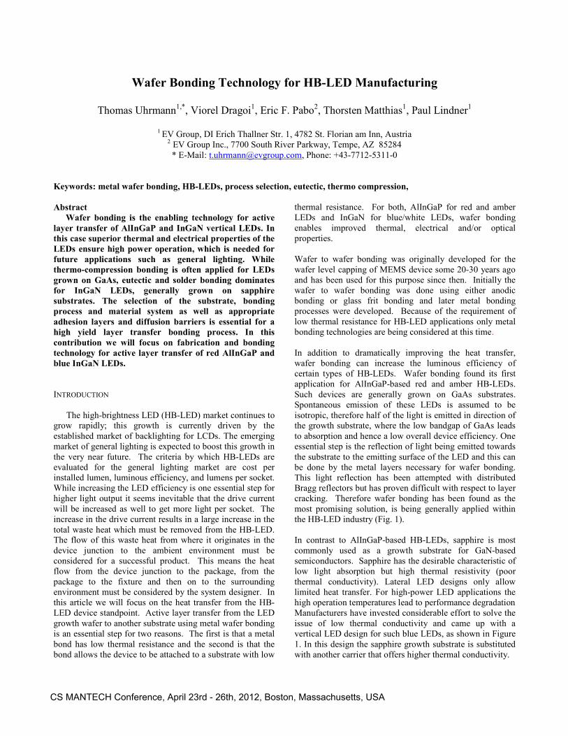
Wafer Bonding Technology for HB-LED Manufacturing
Thomas Uhrmann1,*, Viorel Dragoi1, Eric F. Pabo2, Thorsten Matthias1, Paul Lindner1
1 EV Group, DI Erich Thallner Str. 1, 4782 St. Florian am Inn, Austria2 EV Group Inc., 7700 South River Parkway, Tempe, AZ 85284* E-Mail: [email protected], Phone: +43-7712-5311-0
Keywords: metal wafer bonding, HB-LEDs, process selection, eutectic, thermo compression,
AbstractWafer bonding is the enabling technology for active
layer transfer of AlInGaP and InGaN vertical LEDs. Inthis case superior thermal and electrical properties of theLEDs ensure high power operation, which is needed forfuture applications such as general lighting. Whilethermo-compression bonding is often applied for LEDsgrown on GaAs, eutectic and solder bonding dominatesfor InGaN LEDs, generally grown on sapphiresubstrates. The selection of the substrate, bondingprocess and material system as well as appropriateadhesion layers and diffusion barriers is essential for ahigh yield layer transfer bonding process. In thiscontribution we will focus on fabrication and bondingtechnology for active layer transfer of red AlInGaP andblue InGaN LEDs.
INTRODUCTION
The high-brightness LED (HB-LED) market continues togrow rapidly; this growth is currently driven by theestablished market of backlighting for LCDs. The emergingmarket of general lighting is expected to boost this growth inthe very near future. The criteria by which HB-LEDs areevaluated for the general lighting market are cost perinstalled lumen, luminous efficiency, and lumens per socket.While increasing the LED efficiency is one essential step forhigher light output it seems inevitable that the drive currentwill be increased as well to get more light per socket. Theincrease in the drive current results in a large increase in thetotal waste heat which must be removed from the HB-LED.The flow of this waste heat from where it originates in thedevice junction to the ambient environment must beconsidered for a successful product. This means the heatflow from the device junction to the package, from thepackage to the fixture and then on to the surroundingenvironment must be considered by the system designer. Inthis article we will focus on the heat transfer from the HB-LED device standpoint. Active layer transfer from the LEDgrowth wafer to another substrate using metal wafer bondingis an essential step for two reasons. The first is that a metalbond has low thermal resistance and the second is that thebond allows the device to be attached to a substrate with low
thermal resistance. For both, AlInGaP for red and amberLEDs and InGaN for blue/white LEDs, wafer bondingenables improved thermal, electrical and/or opticalproperties.
Wafer to wafer bonding was originally developed for thewafer level capping of MEMS device some 20-30 years agoand has been used for this purpose since then. Initially thewafer to wafer bonding was done using either anodicbonding or glass frit bonding and later metal bondingprocesses were developed. Because of the requirement oflow thermal resistance for HB-LED applications only metalbonding technologies are being considered at this time.
In addition to dramatically improving the heat transfer,wafer bonding can increase the luminous efficiency ofcertain types of HB-LEDs. Wafer bonding found its firstapplication for AlInGaP-based red and amber HB-LEDs.Such devices are generally grown on GaAs substrates.Spontaneous emission of these LEDs is assumed to beisotropic, therefore half of the light is emitted in direction ofthe growth substrate, where the low bandgap of GaAs leadsto absorption and hence a low overall device efficiency. Oneessential step is the reflection of light being emitted towardsthe substrate to the emitting surface of the LED and this canbe done by the metal layers necessary for wafer bonding.This light reflection has been attempted with distributedBragg reflectors but has proven difficult with respect to layercracking. Therefore wafer bonding has been found as themost promising solution, is being generally applied withinthe HB-LED industry (Fig. 1).
In contrast to AlInGaP-based HB-LEDs, sapphire is mostcommonly used as a growth substrate for GaN-basedsemiconductors. Sapphire has the desirable characteristic oflow light absorption but high thermal resistivity (poorthermal conductivity). Lateral LED designs only allowlimited heat transfer. For high-power LED applications thehigh operation temperatures lead to performance degradationManufacturers have invested considerable effort to solve theissue of low thermal conductivity and came up with avertical LED design for such blue LEDs, as shown in Figure1. In this design the sapphire growth substrate is substitutedwith another carrier that offers higher thermal conductivity.
CS MANTECH Conference, April 23rd - 26th, 2012, Boston, Massachusetts, USA

Figure 1: Schematic of a vertical LED
LED BONDING PROCESS SELECTION
Besides the improved thermal conductivity of vertical HB-LEDs, more benefits can be identified. Compared to thelateral LED design, where the contact to n-GaN is etchedfrom the top side, no etching is needed to manufacture theelectrical contacts. Manufacturing is therefore simplified andthe grown GaN-heterostructure can be used more efficiently.The vertical current path offers another benefit of lowforward bias since a short current path inside thesemiconductor adds a low series resistance. Highlyreflecting layers between GaN and the carrier substrateenable high light extraction efficiency. Aside from that,almost the same process flow can be used for differentvertical LED die sizes.
The overall process flow for the manufacturing of verticalHB-LEDs involves four primary steps: LED layer growth,wafer bonding, removal of the growth substrate andpatterning of the LED dies. In a first step the semiconductorlayers are deposited, as it is usually done by metal organicchemical vapour deposition (MOCVD). The following stepscan be interchanged, depending on the individual processflow of LED manufacturers. While some of them start withthe structurization of the LED dies, others prefer to do thelayer transfer by wafer bonding first. The decision is mainlybeing determined by the downstream processing used toremove the growth substrate. Using laser lift off (LLO) toremove the sapphire substrate induces strain at a die ormultiple die regions due to the decomposition of theinterfacial GaN layer triggered by high power UVirradiation. This introduced strain may lead to cracking ofthe active layers. Confining the strain region by previousstructurization of the dies has been shown to be beneficialwith respect to cracking and yield. For grinding andchemical removal, being mostly applied for AlInGaP LEDs,full-area wafer bonding can be applied before LEDpatterning since no further strain is introduced.
There are four major decisions that must be made whenselecting and setting up a wafer bonding process which are:1. The performance requirements for the bond should beclearly stated. Typically the requirements are good thermalconductivity, adequate mechanical strength and electrical
conductivity. 2. The substrate material must be selected. 3.The bonding process should be selected [1]. 4. The metalstack for the bonding needs to be determined includingadhesion and barrier layers.
For vertical HB-LEDs the bond interface must have highthermal conductivity as well as high electrical conductivity;fortunately for most materials high thermal conductivity alsomeans high electrical conductivity. For this reason, Ge ormetallic substrates are often used. More recently, silicon isemerging as a carrier material, featuring high heatdissipation and low thermal expansion. The possibility toimplement the Zener diode directly into the carrier substrateadds another benefit to vertical HB-LEDs. However, forboth HBLED material systems, whether grown on GaAs orsapphire substrates, active layer transfer is usually done toanother carrier material. Another characteristic that must beconsidered when selecting a substrate material to bond to isthe thermal expansion coefficient (TEC). All common waferto wafer bonding processes require elevated temperatures. Ifthe TEC ratio is more than 2 and at least one material ismechanically weak post-bond wafer bow or even breakagemay occur.
TABLE IMAIN PROCESS FEATURES FOR EUTECTIC AND METAL THERMO-
COMPRESSION WAFER BONDING
Parameter Eutectic BondingThermo-compressionBonding
Temperature Au:Sn - 300°CAu:Si - 380°CAu:Ge - 380°CAl:Ge - 440°CAu:In - 510°C
300°C – 500°C(Au-Au, Cu-Cu,Al-Al)
Temperature range Teutectic + (10°C –20°C)
100°C – 200°C(correlated with contactforce)
Surface Quality Low High
Contact Force Low High
Atmosphere Intert or reducing Inert or reducing
Liquid Phase Yes No
For metal wafer to wafer bonding of HB-LEDs there aregenerally two different fundamental processes used forbonding: the first is using liquid metal to solder the twowafers together (known as solder, eutectic or diffusionbonding) and the second is using the diffusion of the metalatoms across the bond interface (thermo-compressionbonding). The key difference is that in thermo-compressionbonding the metal forming the bond interface is never liquid.From wafer bonding process and equipment perspectivethere are major differences between the two types ofprocesses (table 1).
Solder bonding is a general term for a metal bond formed byliquid metal. This metal could be a pure metal but istypically a binary alloy and in some cases a ternary alloy.
CS MANTECH Conference, April 23rd - 26th, 2012, Boston, Massachusetts, USA

Eutectic wafer bonding alloy is formed at the bondinginterface in a process which goes through a liquid phase: forthis reason, eutectic bonding is less sensitive to surfaceflatness irregularities, scratches, as well as to particlescontamination compared to the direct wafer bondingmethods. Some of the main eutectic alloys used for waferbonding applications are listed in table 1. For a successfuleutectic bonding process it is very important that thebonding equipment has good temperature control andtemperature uniformity across the entire wafer. Temperatureramp for heating/cooling processes are important and haveto be selected based on substrate materials (to avoid thermalshock for dissimilar materials) as well as on devicerequirements (heating/cooling in vacuum or both or onlysingle wafer in contact with heaters). Due to the liquid meltformed during the bond process interfacial particles can beembedded in the melt without creating defects. Good wettingis achieved even on very rough surfaces, which are typicalfor InGaN-based LEDs, contributing to enhanced yield andperformance.
For some HB-LED manufacturing process flows thetemperature must be lower than the bonding temperatures ofthe most usual eutectic alloys (300°C - 400°C). In suchsituations an alternative process can be used, which resultsin an inter-metallic compound bonding layer, known asdiffusion soldering or transient liquid phase (TLP) bonding.This technique uses one thin metal layer (typically 1-10 μm thick) which during a thermal process inter-diffuses with itsbonding partner forming an inter-metallic compound layerwith re-melting temperature higher than the bondingtemperature. Cu-Sn and Au-Sn are the most popular TLPsystems. Same as eutectic wafer bonding, diffusion solderingbonding is attractive for HB-LED manufacturing as they canplanarize over surface defects or particles resulting fromprior processes due to surface wetting by the molten metal.
Finally, in thermo-compression bonding process the twosurfaces adhere to each other due to diffusion of the metalmolecules across the bond interface; this diffusion rate is afunction of the metal, the diffusion barriers on the surface(eg. oxide), the pressure, the temperature and the surfaceroughness. In addition to increasing the fundamentaldiffusion rate, the pressure enhances the diffusion by thedeformation of the two surfaces in contact in order to disruptany intervening surface films and enable increased metal-to-metal contact. As this diffusion continues grain growthoccurs across the bond interface. Heating the metal increasesthe diffusion rate as well as slightly softening the metalswhich increases the deformation for a given pressure. Highforce capability as well as pressure uniformity across thebonding area enables high bonding yield. Several metals areused for metal thermo-compression wafer bonding, as Au-Au, Cu-Cu or Al-Al.
The choice of metal wafer bonding process(eutectic/diffusion soldering or metal thermo-compression)is mainly determined by the properties of the growth andcarrier substrates, such as difference in thermal expansioncoefficient as well as surface properties [1]. For AlInGaPLEDs, which usually have highly flat surface due to theirlattice match to GaAs growth substrates, Au-Au thermo-compression bonding is frequently used. For InGaN LEDson the other hand, the surface roughness and defect densityis considerably larger. Therefore, eutectic or transient liquidphase bonding is regularly used to result in a high yieldingbonding process, as can be seen for Au:Sn bonding in Fig. 2.
Figure 2: SEM cross section image of a InP/GaAs wafer pairafter Au:Sn eutectic wafer bonding
After the metal bonding process has been selected thethickness of and deposition technique must be determinedfor the bonding metals. In addition to the bonding metalstypically adhesion and barrier layers are typically necessaryto ensure sufficient adhesion and that the bonding metals donot migrate into either of the substrates. The selection ofthese adhesion and barrier layers are beyond the scope ofthis article but typically metal layers such as Pt, Al or Auand multilayer combinations of these materials are used.
In addition to selecting a bonding process the process ofaligning the wafers prior to bonding needs to be considered.For HBLED applications mechanical alignment of thesubstrate wafers is typically sufficient this alignment can bedone manually or by the robot when loading the wafers intothe bond chamber or bonding fixtures.
After selecting the overall process flow suitable for thespecific substrate combination and application, a suitablebonding equipment needs to be selected. With theEVG®560HBL, as shown in Fig. 3, we have introduced thefirst wafer bonding equipment dedicated solely to the LEDmarket. The tool is designed for highest yield by optimizedpressure and temperature distribution, combined with an
CS MANTECH Conference, April 23rd - 26th, 2012, Boston, Massachusetts, USA

industry-wide unmet throughput of up to 176 bonds/h (2"wafer equivalents). Both, fully-automated or semi-automatedoperation is possible. The flexible tool supports metal,adhesive and fusion bonds of various substrate types.Cassette-to-cassette operation, multisubstrate bondingcapability and a modular design with up to four swap-inprocess modules make the EVG®560HBL the perfectsolution for high-volume HB-LED manufacturing. EVG'sfield proven wafer bonding technology, as well as ourunique approach to low temperature metal wafer bonding,results in highest throughput and yields.
Figure 3: EVG®560 HBL fully-automated wafer bonderdedicated for HB-LED manufacturing
Wafer bonding is the enabling technology for active layertransfer of AlInGaP and InGaN vertical LEDs. In this casesuperior thermal and electrical properties of the LEDs ensurehigh power operation, which is needed for futureapplications such as general lighting. While thermo-compression bonding is often applied for LEDs grown onGaAs, eutectic and solder bonding dominates for InGaNLEDs grown on sapphire substrates. The selection of thesubstrate, bonding process and material system as well asappropriate adhesion layers and diffusion barriers is essentialfor a high yield bonding process.
CONCLUSION
Wafer bonding is the enabling technology for activelayer transfer of AlInGaP and InGaN vertical LEDs. In thiscase superior thermal and electrical properties of the LEDsensure high power operation, which is needed for futureapplications such as general lighting. While thermo-compression bonding is often applied for LEDs grown on
GaAs, eutectic and solder bonding dominates for InGaNLEDs grown on sapphire substrates. The selection of thesubstrate, bonding process and material system as well asappropriate adhesion layers and diffusion barriers is essentialfor a high yield bonding process.
REFERENCES[1] E.F. Pabo, V. Dragoi, “Wafer Bonding Process Selection”, MEMSIndustry Group
CS MANTECH Conference, April 23rd - 26th, 2012, Boston, Massachusetts, USA