verilog{i | modeling digital hardwarefaculty.cs.tamu.edu/klappi/arch/lab5.pdf · cpsc 321 computer...
TRANSCRIPT

CPSC 321 Computer ArchitectureFall Semester 2004
Lab # 5Introduction to Combinational Circuit ModelingUsing the Verilog Hardware Description Language
Due Date: One week after your lab session
1 Objective
This laboratory assignment introduces the Verilog Hardware Description Language (HDL) and shows youhow to model and simulate basic combinational circuits. HDLs, such as, Verilog, are used extensively in theprocess of designing and implementing digital computer hardware. This writeup includes several tutorialsections on Verilog and it should be used as reference for the rest of the semester.
2 Verilog–I — Modeling Digital Hardware
We start our discussion with the modeling of combinational circuits using the Verilog HDL.
2.1 Verilog’s View of Digital Hardware
Verilog provides the capability to design a digital system in a modular fashion. Entire systems can beviewed as being composed of multiple individual modules. A Verilog module is a system block with welldefined
1. input signals, say x1, x2, . . . , xn,
2. output signals, say y1, y2, . . . , ym, and
3. internal structure and connections or behavior.
Combinational circuits (CCs) produce output signals based on the value of their current input signals. ACC can have any number of input variables (input signals). We consider a CC as a graph of logic gatesinterconnected according to the logic function they compute. CCs route and transform the input valuesto the desired output values. In this graph the vertices correspond to the logic gates and the edges to thewires that connect them together. This graph is a Directed Acyclic Graph (DAG) as it does not includebackward-edges or “loops”. We focus next on the structural description of modules.
2.2 Structural Hardware Modeling
Here we model circuits by specifying the internal structure of the block. It is common to directly use themost primitive building-blocks available, such as, logic gates, or larger blocks which have already beendefined elsewhere. Verilog provides NOT, OR, XOR, NAND, XNOR, NOR gates, among others. Verilogallows each logic gate to have any valid number of inputs. For instance, a single NOR gate can have fourinputs, computing
z = (x1 ⊕ x2 ⊕ x3 ⊕ x4). (1)
In Verilog we can request an XNOR function to be applied to its inputs, as if we were “calling a function”,as follows
1

xnor xnor1( z, x1, x2, x3, x4 );
Usually the output signals in the predefined gates appear first in the argument list of the gate and theinput signals appear afterwards. The identifier xnor1 is associated with this particular instance of anXNOR gate. Identifiers are not mandatory for gate instances. Any other gate can be similarly requestedby mentioning its name and then listing the identifiers that correspond to its output and input signals.For instance the following
or or1( z, x1, x2, x3, x4 );and and1( x1, a, b );and and2( x2, a, c );not not1(na, a);not not2(ne, e);and and3( x3, na, d );and and4( x4, ne, d );
represents in “structural” form the logic network which computes
z = a · b+ a · c+ a · d+ e · d. (2)
The variable names acting as arguments in the logic gate functions, implicitly show the internal connectionsamong the various gates themselves. These variables are of the “wire” type. It is straightforward to describein structural terms any CC, since CCs are DAGs of primitive logic gates. The development of a logic circuitfrom scratch, starting from primitive gates is called structural or “gate-level” modeling.
2.3 Verilog modules, Ports and wires
Gate-level circuit models, quickly become very unwieldy to manage. In Verilog, we can manage thiscomplexity by grouping logic gates together into modules. A module is a subset of the circuit which canbe used as a building block in the design of the entire circuit. Blocks carry out specific functions. A simpleexample is a half or a full adder block with the the well known input and output signals. Verilog declaresmodules bymodule module-identifier.The description of the logic implementing a module is enclosed between the module and the endmodulekeywords. We can declare a module for the circuit computing Eq. 2 of the example above as follows:
module Functionz (z, a, b, c, d, e );output z; /* Output wire (variable) for Functionz */wire z;input a, b, c, d, e; /* Input ‘‘ports’’ */wire x1, x2, x3, x4, na, ne; /* ‘‘Wires’’ for internal connections */
or or1( z, x1, x2, x3, x4 ); /* Instantiation of OR gate ‘or1’ */and and1( x1, a, b ); /* Instantiation of AND gate ‘and1’ */and and2( x2, a, c ); /* etc. */not not1(na, a);not not2(ne, e);and and3( x3, na, d );and and4( x4, ne, d );
endmodule
2

X1 X2 X3 Y1 Y2 Y3
Z2
Z1
LargerSystem
xor2
nand2
xnor2
nor1
or1
and1
xor1
xnor1
or2
nor2
or3
nand1
2
2
2
2
2
b
zc
FunctionZ
z2
1
d
1
1
1
1
e
d
c
b
a
z
2
z1
e
1
FunctionZ
a
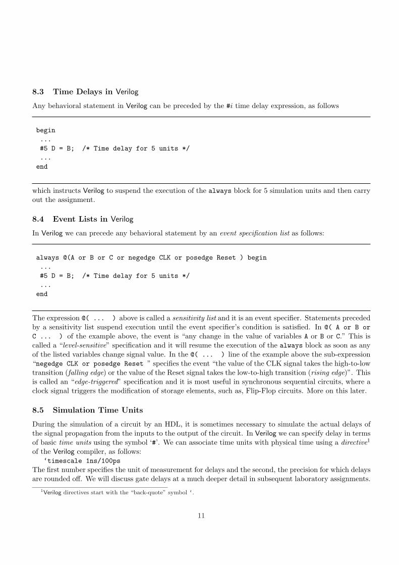
Figure 1: Module LargerSystem consisting of two instances of module Functionz and other logic
Module components can be simple logic gates, as above, or they can be instances of other modules. Modulecomponents are interconnected by wires. Wires represent the actual conductors connecting the output ofa gate to the input of another. In the example above we are using wire x1, x2, x3, x4, na, ne; forthis purpose. A wire is by default a 1-bit signal line.
A Verilog structural model consists of a collection of interconnected modules. Each module defines a setof inputs and outputs connections, called ports. Verilog ports are connection points with other modules inthe system. They are reminiscent of the formal parameters of a procedure in a high level language, in thesense that they allow the module to exchange signals with other modules. Ports can be of mode input,output or inout and by default are of 1-bit in width. A module may receive input signals from its inputports and generate signals to be sent off their output ports. inout ports can at times receive input atother times generate output, but cannot do both simultaneously.
As expected, after the logic for module Functionz has been defined we can use Functionz as a primitivecircuit block of other modules. We discuss the modular system description in the next subsection.
2.4 Hierarchical Specification and Modeling of Hardware Systems
To make a module part of a larger hardware system, we must first “instantiate” it within a higher-levelmodule of this system. By itself, a module definition is just the specification of a circuit, not a part ofthe system itself. This is similar to a type definition in high-level languages where no variable is allocatedactual storage.
To actually add the circuit to the system, we need to create an instance of the associated module andattach it to other modules. Instantiating the module introduces a new physical entity and connects it tothe remaining hardware in the system. Suppose that we want to use our module Functionz as part of a
3

larger system. We will instantiate it from within another module as follows.
module LargerSystem (Z1, Z2, X1, X2, X3, Y1, Y2, Y3 );output Z1, Z2;wire Z1, Z2;input X1, X2, X3, Y1, Y2, Y3; /* Input ‘‘ports’’ */wire a1, b1, c1, d1, e1, z1, a2, b2, c2, d2, e2, z2;
Functionz fz1(z1, a1, b1, c1, d1, e1 ); /* 1st instantiation of Functionz */Functionz fz2(z2, a2, b2, c2, d2, e2 ); /* 2nd instantiation of Functionz */
or or3 (Z1, z1, X1);nand nand1(Z2, z2, Y1);
or or1 (a1, X1, X2);or or2 (b1, Y1, Y2);and and1 (c1, Y3, X3);xnor xnor1(d1, Y2, X2);xor xor1 (e1, Y1, Y2);nor nor1 (a2, X1, X2);nor nor2 (b2, Y1, Y2);nand nand2(c2, Y3, X3);xor xor2 (d2, Y2, X2);xnor xnor2(e2, Y1, Y2);
endmodule
We can see in the above that module LargerSystem includes as a part of its definition a module Functionz.Fig. 1 shows a block schematic of module LargerSystem with two instantiated instances of of moduleFunctionz and other logic. Notice that LargerSystem has two output (Z1, Z2) and six input (X1, X2,X3, Y1, Y2, Y3) signals. Notice How the input for fz1 and fz2 is computed and passed to these twomodules. Notice also how the output signals from fz1 and fz2 are connected to the appropriate parts ofLargerSystem and then it is used to compute the outputs Z1, Z2 of LargerSystem itself. We use wiresthroughout to interconnect modules and ports together.
In a similar fashion we can define systems consisting of blocks that are nested to an arbitrary depth.
3 Assignment–I — Modeling Adder Circuits in Verilog [50 Points]
You will create a Verilog gate-level model of a half-adder circuit, a full-adder and test them with VCSVerilog and a “test-bench” module.
3.1 Addition in Binary
Consider the addition of two 1-bit binary numbers a and b. The result for each possible input combinationis given in the Table 3.1 below: Notice that adding two one-bit values produces a two-bit result. Therightmost (least significant) bit of the result is called the sum, and the leftmost (most significant) bit iscalled the carry out (or simply carry).
4

Table 1: Definition: Binary Addition
a b a+ b
0 0 000 1 011 0 011 1 10
3.2 Assignment–I.1 — Modeling a Half-Adder in Verilog [25 Points]
A half-adder is a combinational circuit that takes two 1-bit inputs a and b, and produces 1-bit outputs sums and carry-out c. The truth table for the 1-bit half-adder is given in Table 2 on page 8 of this handout.We will start by modeling a half-adder in Verilog and testing it with the VCS compiler.Here is a Verilog module for a half-adder:
module halfAdd(sum, cOut, a, b);output sum, cOut;input a, b;
xor (sum, a, b);and (cOut, a, b);
endmodule
The module halfAdd declares four ports, of which two are input and two are output ones. Each portis a signal path that is only one bit wide. We say that size of each port is just one bit. The module isimplemented by a pair of logic gates, an exclusive-or gate (xor) that determines the sum, and an and gatethat determines the carry out. (For gates the output variable is always listed first, followed by the inputvariables).Lab Task: Type the half-adder module into a file and call it Lab5-HA.v.
3.3 Test Modules in Verilog
The Verilog module defined above is not “executable” in any sense. In order to use the module, it mustbe combined with additional Verilog code. We will now create another Verilog module that generates testcases for the half-adder. We implement the test case generator within a Verilog test module. The testmodule is written using Verilog’s behavioral constructs, shown below:
module testAdd(a, b, sum, cOut);input sum, cOut;output a, b;reg a, b;
initial begin$monitor($time, ,"a= %b, b= %b, sum= %b, cOut= %b", a, b, sum, cOut);
a = 0; b = 0;#10 b = 1;#10 a = 1;#10 b = 0;#10 $finish;
5

endendmodule
The test module also declares four ports, corresponding to the ports of the half-adder module. It alsodeclares two “register” variables using the keyword reg, which will store the test values. A register variablein Verilog is a behavioral construct that abstracts the features of an actual register. Registers representsignal values which remain constant until modified. They are typically used in test bench modules to storethe input values of the structural model under test. The size of all port and register variables in thisexample is one bit.
3.4 The $monitor(), $finish() Verilog Tasks and Time Progression
Verilog is a discrete-event simulation language, and the progression of time determines when events mayoccur in the system being simulated. The $monitor argument $time outputs the current simulationtime. In Verilog, time is modeled in discrete time steps with respect to a given unit of time. $time is aninteger variable. The $monitor string argument says to output the values of the four variables in binary.
The initial begin keywords, designate what Verilog should do at simulation $time = 0. We specifyall initializations in the initial blocks. Here the first executable statement is $monitor, which generatesprinted output, in a fashion similar to a printf statement in C). Unlike C, however, the output from$monitor is generated whenever any of the input variables changes value.
The next statement initializes the two 1-bit registers a and b to zero. This will occur at simulation timezero. The next line begins with a delay prefix “#10.” This requires that the interpreter has to “wait” tensimulation time steps before executing the rest of the statement. That is, after delaying until simulationtime 10, register b will be set to one.
Finally, the last statement “$finish,” terminates the simulation and halts Verilog.Lab Task: Type the test module into your file that contains the half-adder.
3.5 initial – Initializing the Simulation of Circuits in Verilog
The initial statement defines a new Verilog thread. A thread is a single execution context, like a processin UNIX, the Windows-PC or a Java thread. Recall that unlike most programming languages, Verilog isused to model parallelism, in which multiple tasks or processes may take place at the same time. One wayto model parallelism in Verilog is to define a new thread for each process. In this simple example, however,we will need only one thread. There are several statements within the body of the thread and are includedwithin the begin and end keywords. The body statements are executed in order from first to last.
3.6 Instantiating the Test Bench Module
Finally, we need to connect the test module to the half adder. A third top level module will do the trick:
module Top;wire sum, cOut, a, b;halfAdd ha(sum, cOut, a, b);testAdd testbenchadd( ); /* YOU MUST COMPLETE THIS LINE */
endmodule
The top level module Top declares an instance of the test-bench module testAdd, named testBencha, andan instance of the module to be tested, halfAdd, named ha.
6

Note that the top level module declares no ports, but there are four variables declared to be wires.Wires are used to connect inputs to outputs.Lab Task: Add the test bench module to your file now. Complete the module by supplying the missingvariables in the test module instance testBencha.
Hint: look at the test module’s definition to see which ports are the inputs and which are the outputs.
3.7 Testing the Verilog Model
You now have a complete Verilog model, ready for testing. To run the model, use the Unix command( You must read section 12 before you can run the following)
vcs -R Lab5-HA.vYou should get the following output in the window. If you do not, then you probably have one or moretyping errors in your input file. Correct them, and try again.
Note: Environment variable $VCS_HOME (/usr/local/synopsys/vcs6.2)overrides default location to find software (/usr/local/VCS)
Note: Environment variable $VCS_VIRSIMHOME (/usr/local/synopsys/virsim_4.2.R2)overrides default location to find Virsim (/usr/local/synopsys/vcs6.2/virsimdir)
***** Warning: Incremental Compile has not been enabled.For faster compiles please add -Mupdate or equivalent flags.
Chronologic VCS (TM)Version 6.2 -- Sun Jun 29 15:29:34 2003Copyright (c) 1991-2002 by Synopsys Inc.
ALL RIGHTS RESERVED
This program is proprietary and confidential information of Synopsys Inc.and may be used and disclosed only as authorized in a license agreementcontrolling such use and disclosure.
Parsing design file ’Lab5-HA.v’Top Level Modules:
TopNo TimeScale specified1 of 3 unique modules to generate1 of 1 modules doneInvoking loader...Chronologic VCS simulator copyright 1991-2002Contains Synopsys proprietary information.Compiler version 6.2; Runtime version 6.2; Jun 29 15:29 2003
0a= 0, b= 0, sum= 0, cOut= 010a= 0, b= 1, sum= 1, cOut= 020a= 1, b= 1, sum= 0, cOut= 130a= 1, b= 0, sum= 1, cOut= 0
$finish at simulation time 40V C S S i m u l a t i o n R e p o r t
Time: 40CPU Time: 0.040 seconds; Data structure size: 0.0Mb
7

Sun xxx xx xx:xx:xx xxxbash-2.03$
Check-off: Answer the following questions and show your answers to the TA for check-off on this part.Which lines of output above were actually generated by the $monitor statement? At what simulation timedid each output line from $monitor occur?
3.8 Lab Part–I.2 — Modeling a Full-Adder in Verilog [25 Points]
Table 2: (a) Truth Table for Half Adder. (b) Truth Table for Full Adder
a b sum carryOut0 0 0 00 1 1 01 0 1 01 1 0 1
(a)
a b carryIn sum carryOut0 0 0 0 00 0 1 1 00 1 0 1 00 1 1 0 11 0 0 1 01 0 1 0 11 1 0 0 11 1 1 1 1
(b)
Lab Task: Now define a 1-bit full-adder in Verilog by combining two half-adders within a new modulecalled fullAdd. A full-adder takes 1-bit inputs a, b, carryIn, and generates 1-bit outputs sum (sum =a+ b+ carryIn) and carryOut. It is the basic building block for the 32-bit MIPS adder circuit. Test yourmodule.
4 Lab Part–II — Modeling Basic Combinational Circuits in Verilog [20Points]
Write test-bench module to exercise the following primitive logic gates:
1. AND,
2. OR,
3. NAND (Not AND),
4. NOR (Not OR),
5. XOR (Exclusive OR),
6. XNOR (Not Exclusive OR).
You need to use three input operands A, B and C and display the result of the corresponding operation,(eg, A NAND B NAND C) for each value of A, B and C, in a tabular form. Your output should includethe three columns for A, B and C and a column for each one of the requested operations above as follows.
8

-----------------------------------------------A B C A&B&C A|B|C . . . .
-----------------------------------------------0 0 0 0 0 . . . .0 0 1 0 1 . . . .. . . . . .1 1 1 1 1 . . . .
-----------------------------------------------
Lab Task: Show the results to your TA for check-off.
5 Lab Part–III — Using Vector Objects in Verilog [20 Points]
So far, we have used Verilog variables to represent single-bit ports, wires, or registers. To model vector(ie, multi-bit) objects, we specify a size when the object is declared, and an index when the variable isreferenced. For example, the following module defines a 4-bit ripple-carry adder using a module for a 2-bitadder with similar inputs and outputs that you will implement later in this part.
module fourBitAdder( a, b, carryIn, sum, carryOut );input [3:0] a, b;input carryIn;output [3:0] sum;output carryOut;wire cOut0;twoBitAdder a1( a[1:0], b[1:0], carryIn, sum[1:0], cOut0 );twoBitAdder a2( a[3:2], b[3:2], cOut0, sum[3:2], carryOut );
endmodule
The expression [3:0] in the port declarations specifies the size of the variables a, b, and sum, as being 4bits wide, each. The expression a[3:2] selects only bits 3 and 2 of the 4-bit port variable a. The expressiona[3] would select only bit 3 of variable a.Lab Requirement Using the 4-bit adder above as an example, implement the 2-bit adder using the one-bit full-adder module from last week’s lab. Modify the test module from Part I to test the 2-bit adder. Besure to extend the test cases appropriately. How many test cases are needed to fully test the 2-bit adder?
Next, add the 4-bit adder module given above to your model and test it. Hint: to test the 4-bit adderexhaustively with every possible input combination would require 512 different test cases, which would bevery tedious. Since you know your 2-bit adder works (you tested it, didn’t you?) you can use this factto simplify testing the 4-bit adder. (Specifically, you need to verify that each 2-bit adder generates thecorrect 2-bit output, and that the carry propagates as expected from the first 2-bit adder to the second,and from the 4-bit carry-in to the first 2-bit adder.)Check-Off: Demonstrate your working two-bit and four-bit adders to your TA for check-off on this part.Note: When printing multi-bit variables using $display or $monitor it may be useful to print their valueeither in hexadecimal, binary, or decimal. You can use the format specifiers %h, %b and %d to output inhexadecimal, in binary, and in decimal, respectively.
6 Lab Part–IV — Basic Combinational Circuits [30 Points]
For this part you are required to design and structurally describe the following multi-bit CCs in Verilog.
9

6.1 Part IV.1 – 5× 32–Decoder
Design and structurally define in Verilog a 32-bit decoder. Add a behavioral model to test-bench yourdesign.Check-Off: Demonstrate your working to your TA for check-off on this part.
6.2 Part IV.2 – 32× 1–Multiplexers
Design and structurally define in Verilog a 32× 1–multiplexer. Add a behavioral model to test-bench yourdesign.Check-Off: Demonstrate your working to your TA for check-off on this part.
7 Lab Part–V — 32-Bit Ripple-Carry Adder/Subtractor [30 Points]
Design and structurally define in Verilog a 32-bit adder/subtractor similar to the one we discussed in class.You can use either 32, one-bit or 4 four-bit adders/subtractors. Add behavioral code to test-bench yourdesign.Check-Off: Demonstrate your working to your TA for check-off on this part.
8 Verilog–II: Behavioral Modeling of Systems
8.1 Verilog Threads
Verilog specifies hardware parallelism using “threads of control.” A new Verilog thread is created by addingbehavioral program statements, enclosed within a begin ... end block in a module. Each of these Verilogthreads progresses in parallel in response to external events, such as, the changing value of input or a freerunning h/w clock. In turn new values computed within a thread trigger future modifications of systemvariables. Threads are behavioral constructs and they play the same role in Verilog as the processes inDiscrete Simulation systems. Threads capture the “natural” concurrency of hardware systems. In Verilogwe can add as many threads to a single model as necessary.
8.2 always and initial Verilog Threads
There are two types of threads: the initial threads and the always ones.An initial thread is specified as an initial begin . . . end block and it is executed once at
$time = 0 (at the beginning of simulation). We use initial threads to initialize system variables and todrive the simulation procedure from the top-level module. initial threads complete as soon as the last(behavioral) statement in their body is executed. initial statements are not synthesizable by the back-end of an integrated design automation system. This means that no actual hardware can be synthesizedout of statements which are preceded by initial.
The always keyword, as in always begin . . . end, introduces an “always” thread which con-tinuously repeats its body in an infinite loop. As before the begin and end keywords define the thread’sbody. always specifies that the thread loops forever. When the last statement in the body is reached,thread execution starts over at the top of the body. always can (and in most cases should) be controlledby simulation time delays. These delays can be specified either as an explicit number of clock units thethread must wait or as events which will cause the thread to resume execution as soon as they take place.
10
8.3 Time Delays in Verilog
Any behavioral statement in Verilog can be preceded by the #i time delay expression, as follows
begin...#5 D = B; /* Time delay for 5 units */...
end
which instructs Verilog to suspend the execution of the always block for 5 simulation units and then carryout the assignment.
8.4 Event Lists in Verilog
In Verilog we can precede any behavioral statement by an event specification list as follows:
always @(A or B or C or negedge CLK or posedge Reset ) begin...#5 D = B; /* Time delay for 5 units */...
end
The expression @( ... ) above is called a sensitivity list and it is an event specifier. Statements precededby a sensitivity list suspend execution until the event specifier’s condition is satisfied. In @( A or B orC ... ) of the example above, the event is “any change in the value of variables A or B or C.” This iscalled a “level-sensitive” specification and it will resume the execution of the always block as soon as anyof the listed variables change signal value. In the @( ... ) line of the example above the sub-expression“negedge CLK or posedge Reset ” specifies the event “the value of the CLK signal takes the high-to-lowtransition (falling edge) or the value of the Reset signal takes the low-to-high transition (rising edge)”. Thisis called an “edge-triggered” specification and it is most useful in synchronous sequential circuits, where aclock signal triggers the modification of storage elements, such as, Flip-Flop circuits. More on this later.
8.5 Simulation Time Units
During the simulation of a circuit by an HDL, it is sometimes necessary to simulate the actual delays ofthe signal propagation from the inputs to the output of the circuit. In Verilog we can specify delay in termsof basic time units using the symbol ‘#’. We can associate time units with physical time using a directive1
of the Verilog compiler, as follows:‘timescale 1ns/100ps
The first number specifies the unit of measurement for delays and the second, the precision for which delaysare rounded off. We will discuss gate delays at a much deeper detail in subsequent laboratory assignments.
1Verilog directives start with the “back-quote” symbol ‘.
11
8.6 Behavioral Modeling for TestBenches and Debugging
We can also use threads to generate the inputs to a system under test at select points of simulation time.The test module we defined for last week’s lab is an example of behavioral modeling with threads. The testmodule contained a single thread (denoted by the initial begin ... end keywords). The thread wasneeded to generate the test cases for the adder circuits, and to display the adder circuit outputs. Finally,because electrical signals require time to propagate through real hardware circuits, Verilog simulates thepassage of time for us. Verilog simulates time as an unsigned integer quantity, and the current simulationtime is always available to us in the predefined integer variable, called $time. By printing out the valueof $time, we can tell when some event took place within our circuit. Learning to appreciate parallelismin real hardware, how to use Verilog threads, and how to mix the structural and behavioral styles is whatmakes using Verilog interesting. In this lab you will learn more about working with Verilog threads.
8.7 Four-valued Logic
Verilog uses a form of four-valued logic rather than the familiar two-valued Boolean logic. The four valuesare
• 0 (zero, false),
• 1 (one, true),
• x which if seen as output means that Verilog does not know how to compute the value for this output(either because it is driven by incompatible signals simultaneously or because no imput is driving it),and
• z high-impedance value.
x and z combine with 0 and 1 in interesting ways. For example, x AND 1 = x, but x AND 0 = 0.
9 Verilog–III — Using Numeric Constants in Verilog
In Verilog constants are specified in the traditional form of a series of digits with or without a sign, butalso in the following form
<size> <base format> <number>
where <size> contains decimal digits that specify the size of the constant in the number of bits. The<size> is optional. The <base format> is the single character “’ ” followed by one of the following
characters b, d, o and h, which stand for binary, decimal, octal and hexadecimal, respectively. The<number> part contains digits which are legal for the <base format>. Some examples:
549 // decimal number’h08FF // 16-bit hexadecimal number4’b11 // 4-bit binary number 11 (0011)3’b10x // 3-bit binary number with least significant bit unknown/don’t care12’o1345 // 12-bit octal number5’d3 // 5-bit decimal number 3 (00011)-4’b11 // 4-bit two’s complement negation of binary number 11 (1101)-4’d3 // 4-bit value decimal number -3 in two’s complement (1101)
12

Note that the <number> part may not contain a sign. Any sign must go on the front.Verilog can use integer, real and even string variables with the corresponding meaning. Integer
variables are used in the simulation process, for instance, by stepping through the various bit positionsof a vector reg or wire variable. Most often it is useful to print out variables of various types for statereporting or debugging purposes. For instance, the code below provides examples on how to use integerand real variables to set the contents of reg variable R1.
// Simple debugging code illustrating how different data types can be //// printed out in Verilogmodule Main;
reg [31:0] R1;integer I;real R;
// Constants can be in decimal or verilog notation //// for (I = -32’d8; I <= 32’d8; I = I + 32’d1) is equivalent to: //initial
beginfor (I = -8; I <= 32’d8; I = I + 32’d1)
begin#1;
R1 = I;R = I;
$display("%0d %0d %b %0d %b %10.2f", $time, I, I, R1,R1, R );
end // for (i=-8; i<=8; i=i+1)$stop;
endendmodule
13