verilog design principles - university of north carolina...
TRANSCRIPT

6-1Logic System Design I
Verilog Design Principles
ECGR2181Extra Notes
�������� ��������
16’h7FEx // 16-bit value, low order 4 bits unknown
8’bxx001100 // 8-bit value, most significant 2 bits unknown.
8’hzz // 8-bit value, all bits high impedance.
FAFA FAFA
A0 B0A1 B1A2 B2A3 B3
c_inc_out
S3 S2 S1 S0
Add_4
c2 c1 c0

Logic System Design I 6-2
Introduction to Hardware Design Languages
What are Hardware Description Languages (HDL)?
“Programming” languages that allow the characteristics of a hardware module to be described.
Many elements analogous to “Software programming”languages:
Declarations of data elements and structures
Description of the sequence of operations which must take place.
Two preeminent HDL’s are Verilog and VHDL.
Logic System Design I 6-3
Introduction to Hardware Design Languages
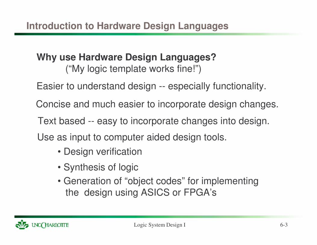
Why use Hardware Design Languages?(“My logic template works fine!”)
Easier to understand design -- especially functionality.
Concise and much easier to incorporate design changes.
Use as input to computer aided design tools.• Design verification
• Synthesis of logic• Generation of “object codes” for implementing
the design using ASICS or FPGA’s
Text based -- easy to incorporate changes into design.
Logic System Design I 6-4
Introduction to Hardware Design Languages
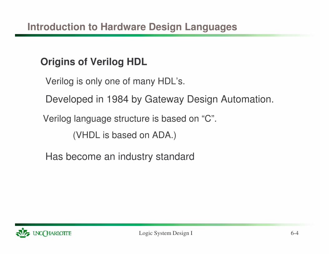
Origins of Verilog HDL
Verilog is only one of many HDL’s.
Verilog language structure is based on “C”.
(VHDL is based on ADA.)
Developed in 1984 by Gateway Design Automation.
Has become an industry standard
Logic System Design I 6-5
Verilog Gate-Level Modeling
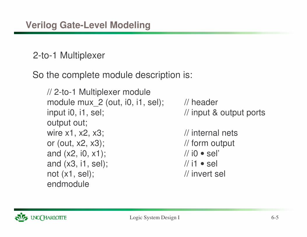
2-to-1 Multiplexer
So the complete module description is:
// 2-to-1 Multiplexer modulemodule mux_2 (out, i0, i1, sel); // headerinput i0, i1, sel; // input & output portsoutput out;wire x1, x2, x3; // internal netsor (out, x2, x3); // form outputand (x2, i0, x1); // i0 • sel’and (x3, i1, sel); // i1 • selnot (x1, sel); // invert selendmodule

Logic System Design I 6-6
Verilog Language Structure
Language conventions:
Whitespace: Blank spaces, tabs and newlines are ignored. Exceptions are when it separates tokens or when it appears in strings.
Case sensitivity: Verilog is case sensitive. Keywords are in lowercase.
Tokens: Verilog code contains a stream of “tokens”. Tokens can be comments, delimiters, numbers, strings, identifiers and keywords.

Logic System Design I 6-7
Verilog Language Structure
Language conventions:
A multiple-line comment begins with “/*” and ends with “*/”. Multi-line comments cannot be nested.
/* This is a multiple linecomment*/
Comments: Comments follow normal “C” conventions.
A “//” starts a one-line comment. Everything that appears after the “//” to the end of line (newline) is
treated as a comment.
a = b && c; // The rest of this line is a comment

Logic System Design I 6-8
Verilog Language Structure
Language conventions:
Operators: There are three types of operators:
Unary - single operand. Operator precedes operand.
Binary - two operands. Operator appears betweenthe two operands.
Ternary - three operands. Two operators separatethe three operands.
Statement terminator: Most Verilog statements end with a semicolon.
Logic System Design I 6-9
Verilog Language Structure
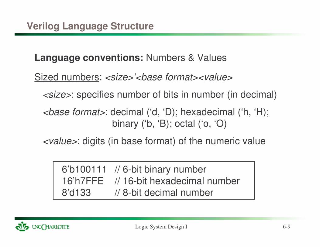
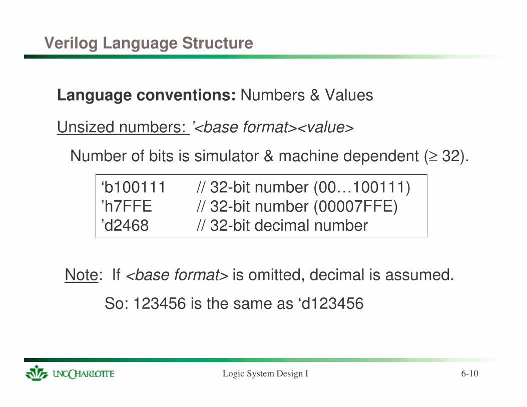
Language conventions: Numbers & Values
Sized numbers: <size>’<base format><value>
<size>: specifies number of bits in number (in decimal)
<base format>: decimal (‘d, ‘D); hexadecimal (‘h, ‘H);binary (‘b, ‘B); octal (‘o, ‘O)
<value>: digits (in base format) of the numeric value
6’b100111 // 6-bit binary number16’h7FFE // 16-bit hexadecimal number8’d133 // 8-bit decimal number
Logic System Design I 6-10
Verilog Language Structure
Language conventions: Numbers & Values
Unsized numbers: ’<base format><value>
Number of bits is simulator & machine dependent (≥ 32).
‘b100111 // 32-bit number (00…100111)’h7FFE // 32-bit number (00007FFE)’d2468 // 32-bit decimal number
Note: If <base format> is omitted, decimal is assumed.
So: 123456 is the same as ‘d123456

Logic System Design I 6-11
Verilog Language Structure
Language conventions: Numbers & Values
In addition to normal numeric values, Verilog provides two special values, x and z.
x denotes an unknown or undefined value.
z denotes a “high impedance” value
16’h7FEx // 16-bit value, low order 4 bits unknown
8’bxx001100 // 8-bit value, most significant 2 bits unknown.
8’hzz // 8-bit value, all bits high impedance.

Logic System Design I 6-12
Verilog Language Structure
Language conventions: Numbers & ValuesZero fill / extension: If a numeric value does not contain enough digits to fill the specified number of bits, the high order bits are filled with zeros. If the most significant bit specified is an x or z, the x/z is left extended to fill the bit field.
16’h39 � 16’h0039 � 0000 0000 0011 1001
8’hz � 8’hzz � zzzz zzzz
Negative numbers: Specified by preceding the <size>with a minus (negative) symbol. Values will be stored as the two’s complement of the given value.
Logic System Design I 6-13
Verilog Language Structure
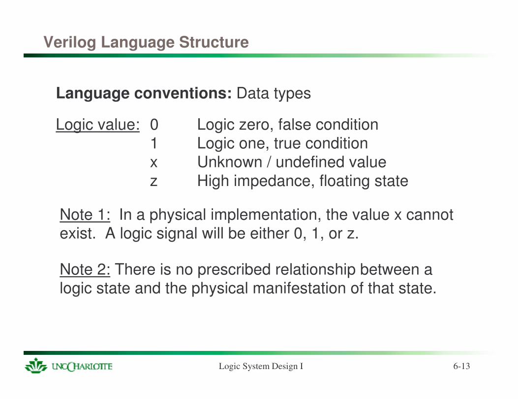
Language conventions: Data types
Logic value: 0 Logic zero, false condition1 Logic one, true conditionx Unknown / undefined valuez High impedance, floating state
Note 1: In a physical implementation, the value x cannot exist. A logic signal will be either 0, 1, or z.
Note 2: There is no prescribed relationship between a logic state and the physical manifestation of that state.

Logic System Design I 6-14
Verilog Language Structure
Language conventions: Nets, Registers & Vectors
Nets are declared by keyword wire.
Nets represent connections between hardware components.
wire d; // declare output as net d.wire b, c; // declare two wires in same statement
a, b, c, & d are nets.
a
b cd
Logic System Design I 6-15
Verilog Language Structure
Language conventions: Nets, Registers & Vectors
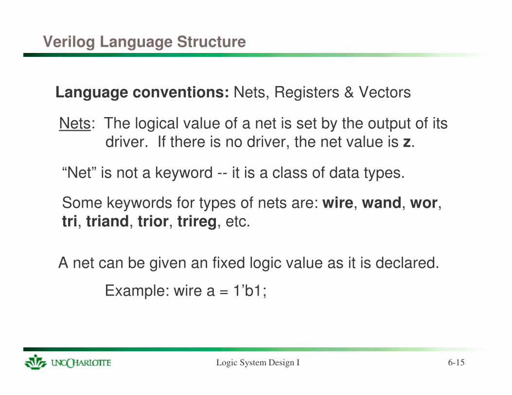
Nets: The logical value of a net is set by the output of itsdriver. If there is no driver, the net value is z.
“Net” is not a keyword -- it is a class of data types.
Some keywords for types of nets are: wire, wand, wor, tri, triand, trior, trireg, etc.
A net can be given an fixed logic value as it is declared.
Example: wire a = 1’b1;

Logic System Design I 6-16
Verilog Language Structure
Language conventions: Nets, Registers & Vectors
Registers provide data storage. In Verilog, registersimply means a variable that can hold a value.
A Verilog register is not the same as a hardware register.
A register does not need a driver. They also do not need a clock like a hardware register does. Values are changed by assigning a new value to the register.
Confused? In Verilog, we do not explicitly declarehardware registers. The context of the
description determines if a physicalregister exists.

Logic System Design I 6-17
Verilog Language Structure
Language conventions: Nets, Registers & Vectors
Registers are declared by the keyword reg. The default value for a reg data type is x.
reg start; // declares register “start”
reg reset, clock; // declares registers reset & clock
Vector & scalar data types: Nets and reg data types can be declared as vectors (multiple-bit data) or as scalars (single-bit data). If the width of a data variable is not declared, scalar is assumed.

Logic System Design I 6-18
Verilog Language Structure
Language conventions: Nets, Registers & Vectors
Vector and scalar declarations
Vectors can be specified by declaring the range of bit numbers with the variable name. The form of the declaration is: [<high#>: <low#>] <variable> ;
or [<low#>: <high#>] <variable> ;
wire [7:0] BYTE; // declare 8-bit data.reg [15:0] INFO; // declare 16-bit register.reg [0:11] DATA; // declare 12-bit register

Logic System Design I 6-19
Verilog Language Structure
Language conventions: Nets, Registers & Vectors
Note: The bit numbers can run in either direction but the left-hand number of the pair in the brackets is always the most significant bit of the vector.
So, in the following declarations:reg [15:0] INFO; // declare 16-bit register.reg [0:31] DATA; // declare 32-bit register
bit 15 of INFO and bit 0 of DATA are the MSB’s.
Note: For lecture, notes, etc. I will be assuming that bit 0 will be the Least Significant Bit. .

Logic System Design I 6-20
Verilog Language Structure
Language conventions: Nets, Registers & Vectors
Note: While bit numbering in a declaration conventionally includes bit 0, it is not required. wire [1:10] STUFF; is also a valid declaration.
So: For those who are “zero challenged” you could number the bits of a byte as 8:1 instead of 7:0. Just bear in mind, all class notes will use the “zero-relative”numbering.

Logic System Design I 6-21
Verilog Language Structure
Language conventions: Nets, Registers & Vectors
As seen from previous examples of scalar declaration, multiple vectors can be declared on a single line. So the declaration of INFO and DATA from above could be written as:
reg [15:0] INFO, [31:0] DATA;
Likewise, the declaration of 8-bit registers A, B & C could be written as:
reg [7:0]A, [7:0]B, [7:0]C;
Logic System Design I 6-22
Verilog Language Structure
Language conventions: Nets, Registers & Vectors
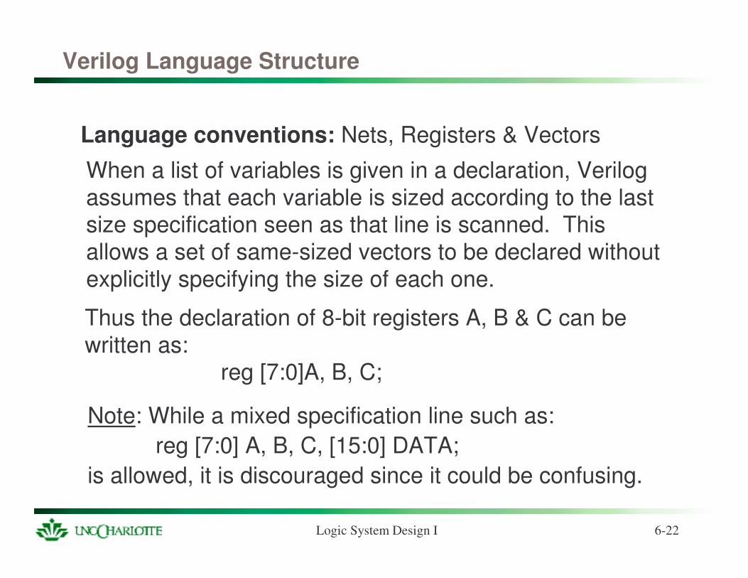
When a list of variables is given in a declaration, Verilog assumes that each variable is sized according to the last size specification seen as that line is scanned. This allows a set of same-sized vectors to be declared without explicitly specifying the size of each one.
Thus the declaration of 8-bit registers A, B & C can be written as:
reg [7:0]A, B, C;
Note: While a mixed specification line such as:reg [7:0] A, B, C, [15:0] DATA;
is allowed, it is discouraged since it could be confusing.

Logic System Design I 6-23
Verilog Language Structure
Language conventions: Nets, Registers & Vectors
Specifying parts of vectors: Given vector declarations, it is possible to reference parts of a register (down to a single bit). The format of the reference follows the pattern <vector> [ <bit range>].
INFO [5] // bit 5 of INFOINFO [11:8] // second nibble of INFO (bits 11-8)DATA [7:0] // most significant byte of DATA

Logic System Design I 6-24
Verilog Language Structure
Language conventions:
Integer data type: A general purpose register data type for manipulating integer values. They are declared by the keyword integer. Values are 32 bit signed values.
These are rarely used in the description of a hardware module but are frequently useful in the Test Fixture.
Time data type: A special register which tracks simulation time. Declared with keyword time. A system function $time accesses the current simulation time.

Logic System Design I 6-25
Verilog Language Structure
Module interconnections: Ports
A digital module must have the ability to interconnect with its environment. This requires the definition of input and output ports.
It is through these ports that all information is passed between modules. Thus an integral part of the definition of a module is the declaration of its ports.

Logic System Design I 6-26
Verilog Language Structure
Module interconnections: PortsThere are three types of ports which can be declared in Verilog.
input Input only portoutput Output only port inout Bidirectional port
Ports are declared with the syntax: <port_type> { [<size>] } <name>
input clock, reset; // single bit input signalsinput [15:0] DATA; // 16-bit input wordoutput data_strobe; // single-bit output signaloutput [7:0] RESULT; // output byte

Logic System Design I 6-27
Verilog Language Structure
Module interconnections: PortsWithin a Verilog system model, module interconnections occur at two levels:
• Peer to peer: modules interconnect with each other:
Module A Module B
Module A
Module B
• Hierarchical: one module incorporates the other.

Logic System Design I 6-28
Verilog Language Structure
Module interconnections: PortsPort connections must observe a set of rules about the type of signal (both internal & external) they connect to.
Inputs: Internally ports must be a net (typ. Wire). Theexternal source may be either a reg or a net.
Outputs: The internal source for an output port can beeither a reg or a net. The external destinationmust be a net.
Inouts: The inout ports must be connected to nets bothinternally and externally.

Logic System Design I 6-29
Gate-Level Modeling : Basic elements
Gate-level modeling is the lowest level of design description in Verilog.(Actually there is a lower level -- transistor level.)
Verilog models at the gate level consists of directly specifying the interconnections of fundamental logic elements (AND, OR, etc.).
The available logic elements at the gate level are: and, nand, or, nor, xor, xnor, not, buf, notif & bufif.
(All these are keywords.)

Logic System Design I 6-30
Gate-Level Modeling : Basic elements
The functionality of these basic logic gates are self-explanatory with the exception of buf, notif & bufif.
buf is simply a non-inverting buffer gate. It is transparent from a logical sense but may be required for implementation.
notif & bufif are tri-state versions of the not & bufgates. These gates have a extra control line which enables the gate when true and places the gate into the high-impedance z state when false.

Logic System Design I 6-31
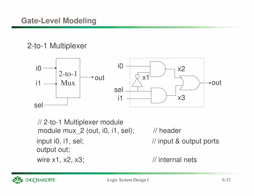
Gate-Level Modeling
Description of a module at the gate level consists of the declarations (header, ports, variables) and a series of instantiations of the base logic elements. Through the instantiations, the wiring of the module is specified.
The format of a gate-level instantiation is:<gate_type> <i_name> (<out_name>, <in_name_list);
and q1 (q1_out, q1_in1, q1_in2); // 2-input ANDor q2 (q2_out, q2_in1, q2_in2, q2_in3); // 3-input ORnot q3 (q3_out, q3_in); // inverternotif q4 (q4_out, q4_in, control); // tri-state inverter
Logic System Design I 6-32
Gate-Level Modeling
2-to-1 Multiplexer
x2x1
x3
out2-to-1Mux
i0
i1
sel
i0
seli1
out
// 2-to-1 Multiplexer modulemodule mux_2 (out, i0, i1, sel); // headerinput i0, i1, sel; // input & output portsoutput out;wire x1, x2, x3; // internal nets
Logic System Design I 6-33
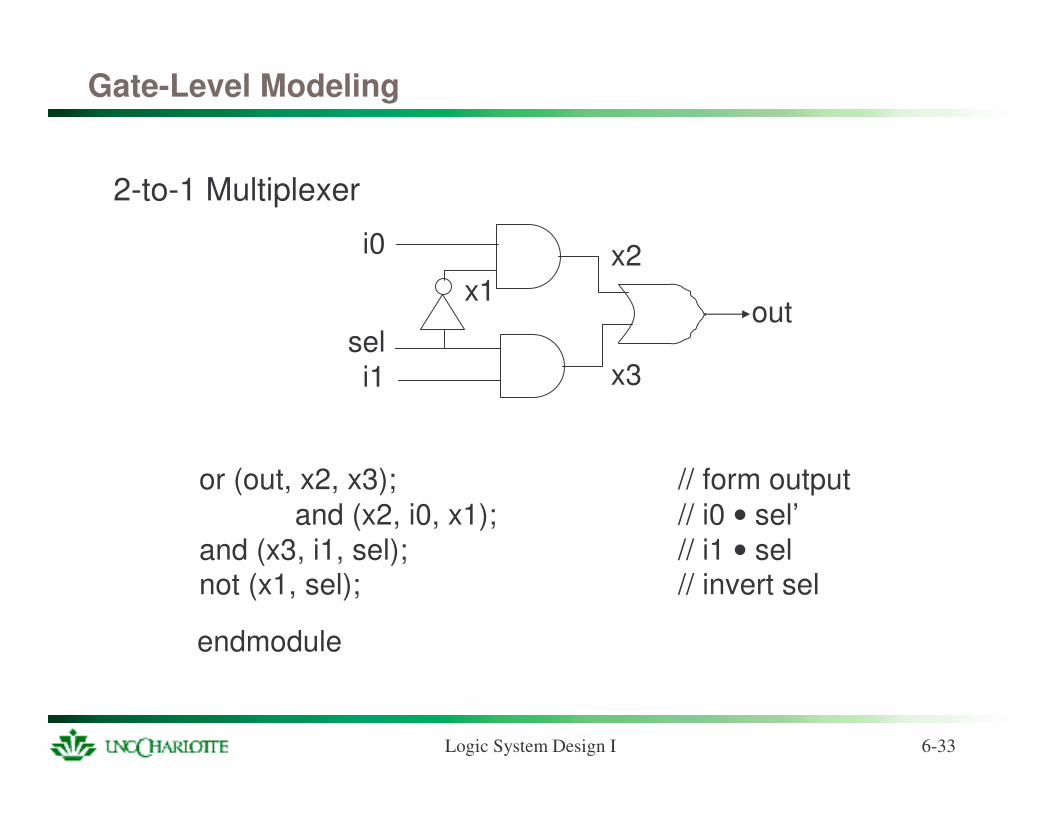
Gate-Level Modeling
2-to-1 Multiplexer
or (out, x2, x3); // form outputand (x2, i0, x1); // i0 • sel’
and (x3, i1, sel); // i1 • selnot (x1, sel); // invert sel
endmodule
x2x1
x3
i0
seli1
out

Logic System Design I 6-34
Gate-Level Modeling
2-to-1 Multiplexer
So the complete module description is:
// 2-to-1 Multiplexer modulemodule mux_2 (out, i0, i1, sel); // headerinput i0, i1, sel; // input & output portsoutput out;wire x1, x2, x3; // internal netsor (out, x2, x3); // form outputand (x2, i0, x1); // i0 • sel’and (x3, i1, sel); // i1 • selnot (x1, sel); // invert selendmodule

Logic System Design I 6-35
Dataflow Modeling
Continuous assignment
The next level of design abstraction above gate-level design is dataflow. Dataflow descriptions are created with the use of continuous assignment statements.
A continuous assignment statement begins with the keyword assign. The format of a continuous assignment statement is:
assign <variable_name> = <assignment>;where <assignment> is a constant, variable or expression
Logic System Design I 6-36
Dataflow Modeling
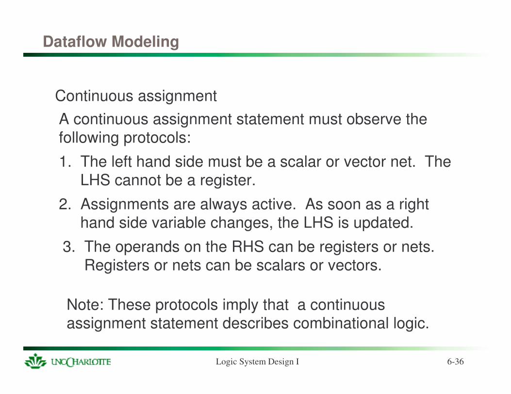
Continuous assignmentA continuous assignment statement must observe the following protocols:
1. The left hand side must be a scalar or vector net. TheLHS cannot be a register.
2. Assignments are always active. As soon as a righthand side variable changes, the LHS is updated.
3. The operands on the RHS can be registers or nets.Registers or nets can be scalars or vectors.
Note: These protocols imply that a continuous assignment statement describes combinational logic.

Logic System Design I 6-37
Dataflow Modeling
Continuous assignmentTypical assign statements are:. assign out = i1 & i2; // out is a scalar net, i1 & i2 are
// scalar nets or registers
assign SUM = A + B; // SUM is a vector net, A & B//are vector nets or registers
In addition to writing an assign statement in the body of the module description, it can also be written as part of the declaration of the net which receives its result.
wire out;assign out = in1 & in2;
wire out = in1 & in2;
Logic System Design I 6-38
Dataflow Modeling
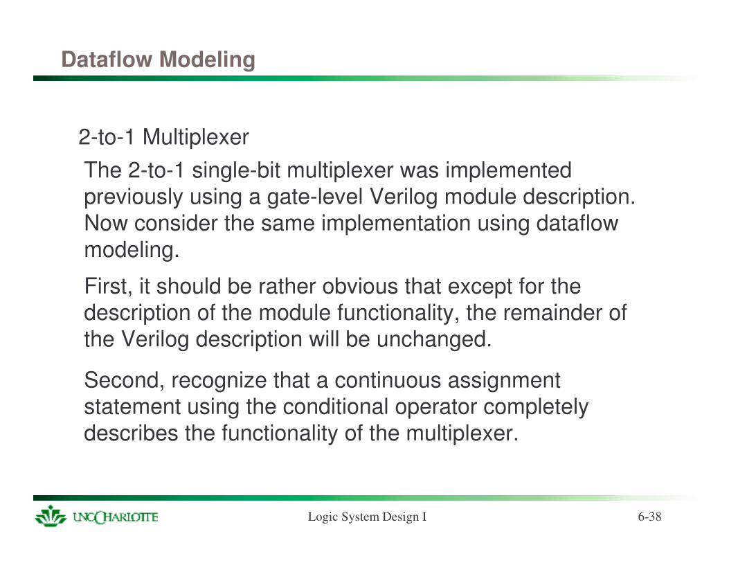
2-to-1 MultiplexerThe 2-to-1 single-bit multiplexer was implemented previously using a gate-level Verilog module description. Now consider the same implementation using dataflow modeling.
First, it should be rather obvious that except for the description of the module functionality, the remainder of the Verilog description will be unchanged.
Second, recognize that a continuous assignment statement using the conditional operator completely describes the functionality of the multiplexer.

Logic System Design I 6-39
Dataflow Modeling
2-to-1 Multiplexer
So, the revised module description becomes:
// 2-to-1 Multiplexer modulemodule mux_2 (out, i0, i1, sel); // headerinput i0, i1, sel; // input & output portsoutput out;assign out = sel ? i1 : i0; // cont. assignm’t for muxendmodule

Logic System Design I 6-40
Dataflow Modeling
4-bit Multiplexer
Given the simplicity of implementing the 2-to-1 Multiplexer at the dataflow level, now consider the 4-bit Multiplexer.
With a modest amount of thought we realize that the Verilog description for the 4-bit Multiplexer will be virtually identical to the single-bit unit.
The only difference is that the input and output data are vectors instead of scalars.

Logic System Design I 6-41
Dataflow Modeling
4-bit Multiplexer
So the code for the 4-bit mux becomes:
// Four-bit 2-to-1 multiplexermodule mux_4bit (Out, A, B, sel);input [3:0] A, B;input sel;output [3:0] Out;assign Out = sel ? B, A;endmodule
And we don’t need to incorporate the mux_2 module into this module.
Logic System Design I 6-42
Behavioral Modeling
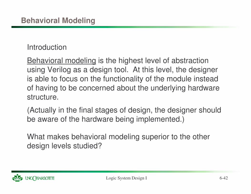
Introduction
Behavioral modeling is the highest level of abstraction using Verilog as a design tool. At this level, the designer is able to focus on the functionality of the module instead of having to be concerned about the underlying hardware structure.
(Actually in the final stages of design, the designer should be aware of the hardware being implemented.)
What makes behavioral modeling superior to the other design levels studied?

Logic System Design I 6-43
Behavioral Modeling
StructureThe basic element of the structure of a behavioral description is the procedural block.
A behavioral module description may contain one or more procedural blocks.
Verilog provides two types of procedural blocks: the initial block and the always block.
In a programming language like C, statement execution is sequential and mutually exclusive. On the other hand, Verilog is a concurrent language. So activities in Verilog run concurrently. The initial and always blocks define these concurrent structures.

Logic System Design I 6-44
Behavioral Modeling
Structure
Within procedural blocks, related sequences of behavioral statements must be grouped. In Verilog, these statements are grouped between the keywords begin and end.
(These keywords fit in the language context similar to the { and } characters which group statements in C.)
If the procedural block contains only a single behavioral statement, the begin and end are not necessary.
Also note that begin and end are not terminated with a semicolon.

Logic System Design I 6-45
Behavioral Modeling
Always blocks
A digital module is normally a continuously active unit. All sequential machines (which covers most digital modules) require either an external signal or a synchronizing clock to cause them to step through their sequence of operation.
This continuous (and often synchronized) operation is provided by the always procedural block. The alwaysblock starts at time 0 and continuously executed the behavioral statements inside the block continuously (read loop).
Logic System Design I 6-46
Behavioral Modeling
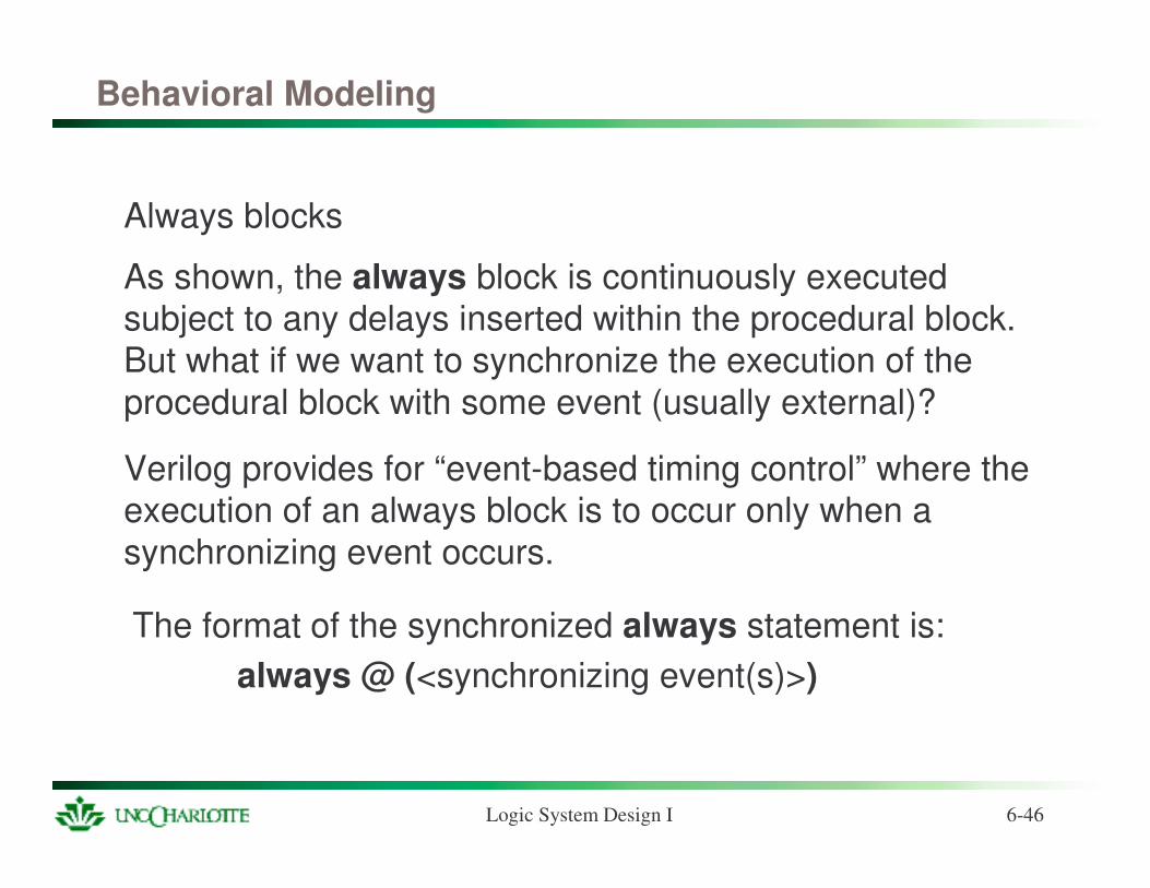
Always blocks
As shown, the always block is continuously executed subject to any delays inserted within the procedural block. But what if we want to synchronize the execution of the procedural block with some event (usually external)?
Verilog provides for “event-based timing control” where the execution of an always block is to occur only when a synchronizing event occurs.
The format of the synchronized always statement is:always @ (<synchronizing event(s)>)

Logic System Design I 6-47
Behavioral Modeling
Always blocks
A <synchronizing event> can be one of the following:
• Execute whenever the value of the listed variablechanges. .
always @ (clock) executes its procedural block whenever clock changes state
always @ (A) executes its procedural blockwhenever the value of vector Achanges.

Logic System Design I 6-48
Behavioral Modeling
Always blocks
In addition to the simple synchronizing events listed, they can be combined to provide multiple events which trigger the procedural block. Here, the triggering events are Ored.
always @ (A or B) executes the proceduralblock whenever A orB changes value.

Logic System Design I 6-49
Behavioral Modeling
Procedural AssignmentsThe left-hand side of a procedural assignment can be any of the following:
•A reg, integer or memory element.SUM = A + B; // SUM is set to A + B
•A bit-select of a variable.SR[5] = &Q; // Set bit 5 of SR to 1 if Q is all 1’s
• A part-select of a variable.SR[2:1] = i_lev; // Set bits 2 & 1 to the value of I_lev.
•A concatenation of any of the above.
Logic System Design I 6-50
Behavioral Modeling
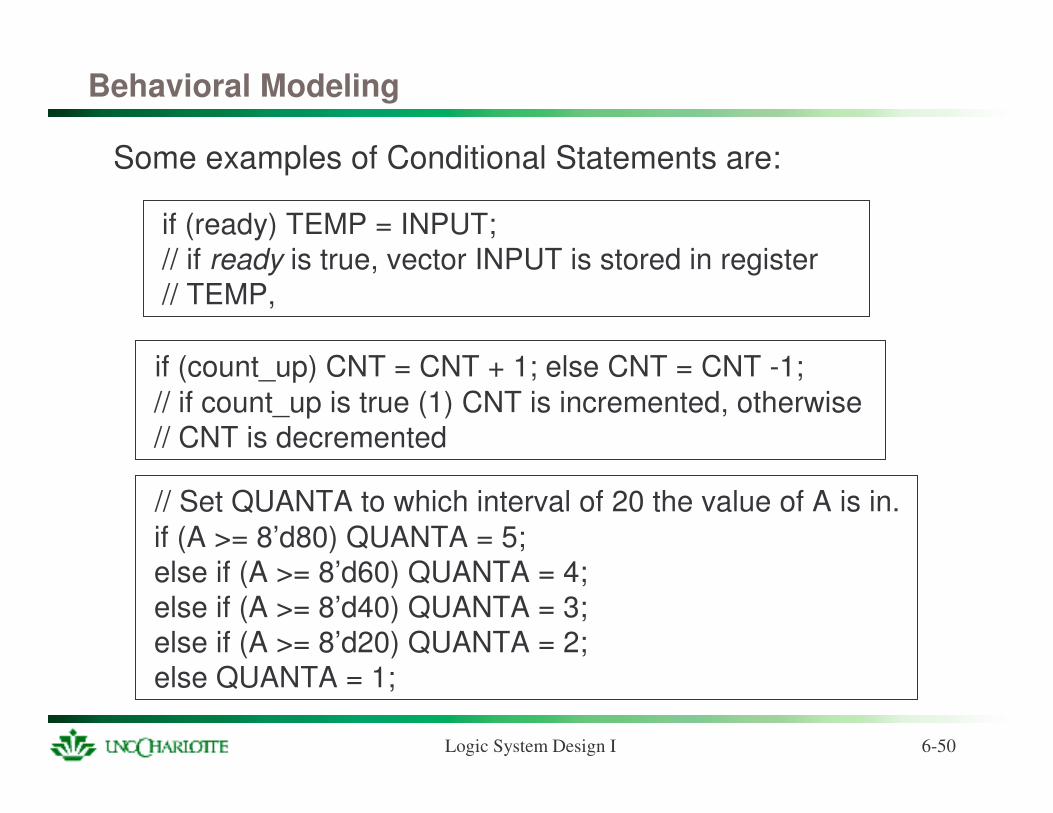
Some examples of Conditional Statements are:
if (ready) TEMP = INPUT;// if ready is true, vector INPUT is stored in register// TEMP,
if (count_up) CNT = CNT + 1; else CNT = CNT -1;// if count_up is true (1) CNT is incremented, otherwise// CNT is decremented
// Set QUANTA to which interval of 20 the value of A is in.if (A >= 8’d80) QUANTA = 5;else if (A >= 8’d60) QUANTA = 4;else if (A >= 8’d40) QUANTA = 3;else if (A >= 8’d20) QUANTA = 2;else QUANTA = 1;

Logic System Design I 6-51
Behavioral Modeling
Conditional StatementsThe syntax of the case statement is:
case (<expression>)<alternative 1>: <statement 1*>;<alternative 2>: <statement 1*>;
• • •<alternative n>: <statement n*>;default: <default statement*>;
endcase
The value of <expression> is matched to <alternatives> in sequence, For the first <alternative> that matches, the corresponding <statement> is executed. If no alternatives match, <default statement> is executed.

Logic System Design I 6-52
Behavioral Modeling
Conditional StatementsUsing the previous example of an ALU, the corresponding implementation using a case statement is:
case (alu_ctrl)3’d0: ALU_OUT = ALU_IN1 + ALU_IN2;3’d1: ALU_OUT = ALU_IN1 - ALU_IN2;3’d2: ALU_OUT = ALU_IN1 & ALU_IN2;3’d3: ALU_OUT = ALU_IN1 | ALU_IN2;3’d4: ALU_OUT = ALU_IN1 ^ ALU_IN2;default: ALU_OUT = 16’d0;
endcase
Which may not be significantly more compact than the if - else if - else implementation but is more readable.

Logic System Design I 6-53
Behavioral Modeling
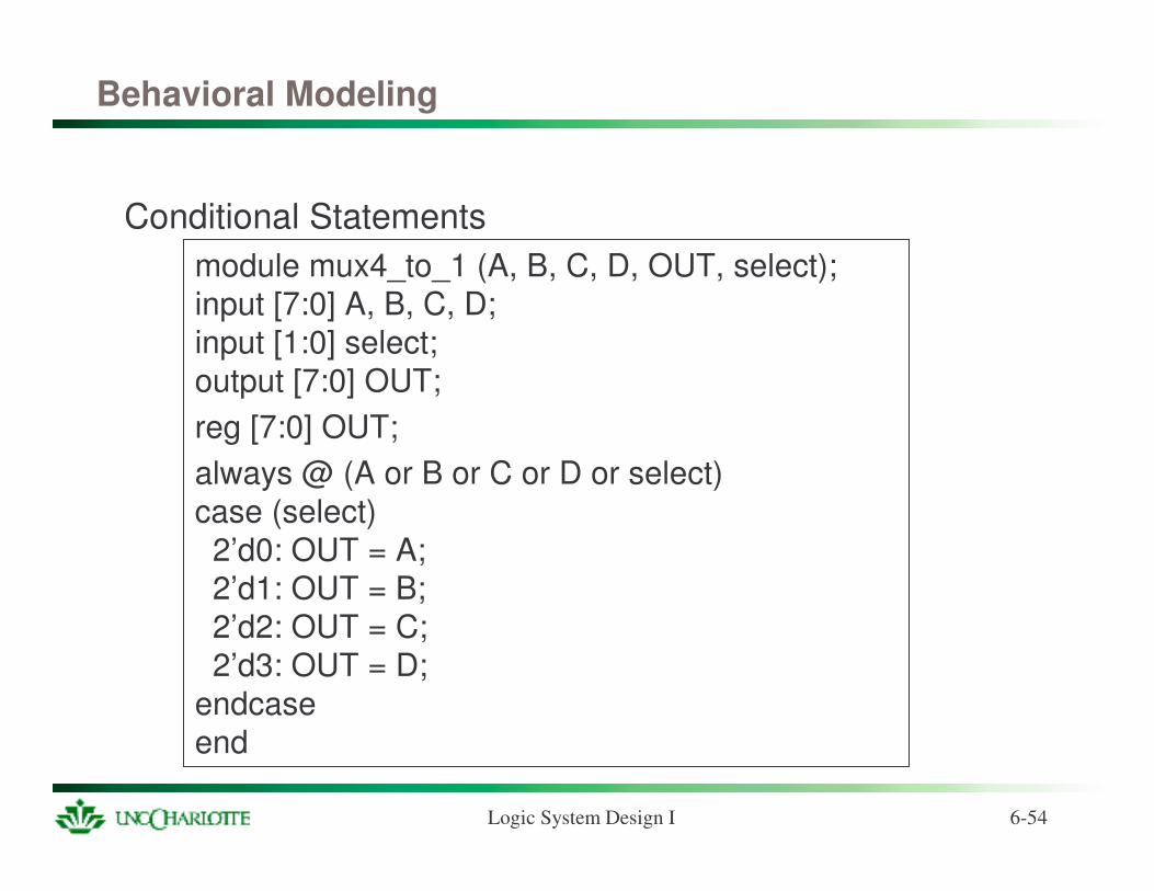
Conditional StatementsIn some respects, the case statement acts like a many-to-one multiplexer, i.e. selecting one result from a number of possible results.
With this in mind, consider modeling a byte-wide four-to-one multiplexer, e.g. select 1 of four bytes for output.
4-to-1Mux
ABCD
select
OUT
Logic System Design I 6-54
Behavioral Modeling
Conditional Statementsmodule mux4_to_1 (A, B, C, D, OUT, select);input [7:0] A, B, C, D;input [1:0] select;output [7:0] OUT;reg [7:0] OUT;always @ (A or B or C or D or select)case (select)
2’d0: OUT = A;2’d1: OUT = B;2’d2: OUT = C;2’d3: OUT = D;
endcaseend