university of salamanca, spain - fapesp of salamanca, spain ... thz radiation can be used to...
TRANSCRIPT

Nanodevices for THz Applications
Tomás González University of Salamanca, Spain
Research Group on
Semiconductor Devices
T. González - Nanodevices for THz Applications December 12, 2012
THz Nanodevices at USAL
Research Group on Semiconductor Devices
- Modeling of nanodevices for THz applications
- Design of optimized structures (feedback to technology)
THz Laboratory
- Detection and emission of THz radiation from plasma wave nanodevices
- Time-domain spectroscopy and imaging in the THz range

http://campus.usal.es/~gelec/ CONTACT: Prof. Tomás González ([email protected])
Monte Carlo simulation of high-frequency nanodevices
Characterization Laboratory (DC-GHz) Semiconductor Nanodevices for Room Temperature
THz Emission and Detection - http://www.roothz.eu/
Coordinator of the FP7 STREP Project ROOTHz (FP7-243845)
GaN diodes InGaAs/InAlAs diode
100nm
Advanced Si MOSFETs (FP6 project METAMOS)
InGaAs/InAlAs, InAs/AlSb and GaN/AlGaN HEMTs
InGaAs based THz ballistic nanodevices (FP5 project NANOTERA )
TBJs YBJs MUX/DEMUX SSDs
Staff: 8 permanent researchers, 3 post-doc, 2 students
Collaborations with several EU (IEMN, Chalmers, Manchester, Montpellier, etc.) and USA Labs. (Rochester)
RESEARCH LINES
Research Group on Semiconductor Devices
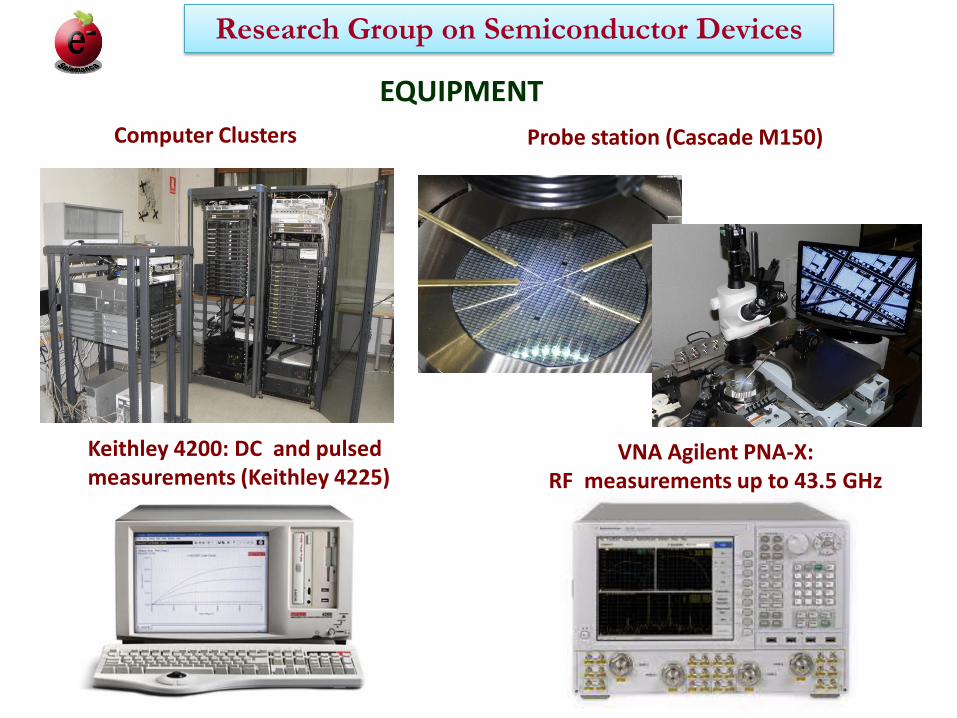
EQUIPMENT
Computer Clusters
Keithley 4200: DC and pulsed measurements (Keithley 4225)
Probe station (Cascade M150)
VNA Agilent PNA-X: RF measurements up to 43.5 GHz
Research Group on Semiconductor Devices
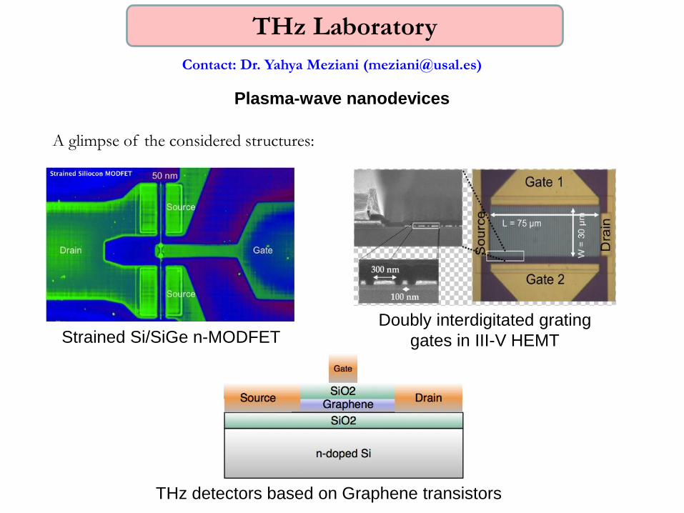
Doubly interdigitated grating
gates in III-V HEMT Strained Si/SiGe n-MODFET
THz detectors based on Graphene transistors
A glimpse of the considered structures:
THz Laboratory
Contact: Dr. Yahya Meziani ([email protected])
Plasma-wave nanodevices
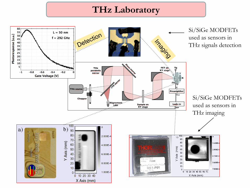
Si/SiGe MODFETs
used as sensors in
THz signals detection
Si/SiGe MODFETs
used as sensors in
THz imaging
THz Laboratory

Facilities
Terahertz Spectroscopy System
THz-Time Domain Spectroscopy System: EKSPLA
Spectrometer+Ti:Sapphire Laser (Spectra-Physics)
THz imaging: Gunn Diode at 0.2TH + frequency tripler
Probestation
Cascade Summit 11000B manual probestation with
FemtoGuard® and PurelineTM technologies (200mm-chuck)
+ Agilent B1500 (4 SMUs, 1 multifreq CMU and 1 WG/FMU
THz Laboratory

T. González - Nanodevices for THz Applications December 12, 2012
Introduction. Importance of THz
ROOTHz Project
Self Switching Diodes (SSDs)
Conclusions / Perspectives
Outline
Outline
T. González - Nanodevices for THz Applications December 12, 2012
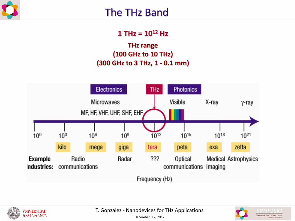
1 THz = 1012 Hz
THz range (100 GHz to 10 THz)
(300 GHz to 3 THz, 1 - 0.1 mm)
The THz Band

T. González - Nanodevices for THz Applications December 12, 2012
Image of sea surface temperature (European Space Agency)
THz radiation can penetrate poor weather, dust and smoke far better than infrared or visible systems.
Satellite Telemetry
Aeronautics: guidance and landing
Potential applications

T. González - Nanodevices for THz Applications December 12, 2012
THz radiation can penetrate organic materials without ionizing
Readily absorbed by water: distinguish between materials with varying water content
Medical imaging
Courtesy of Teraview Courtesy of Teraview
Skin Cancer Detection
Potential applications: medical diagnosis

T. González - Nanodevices for THz Applications December 12, 2012
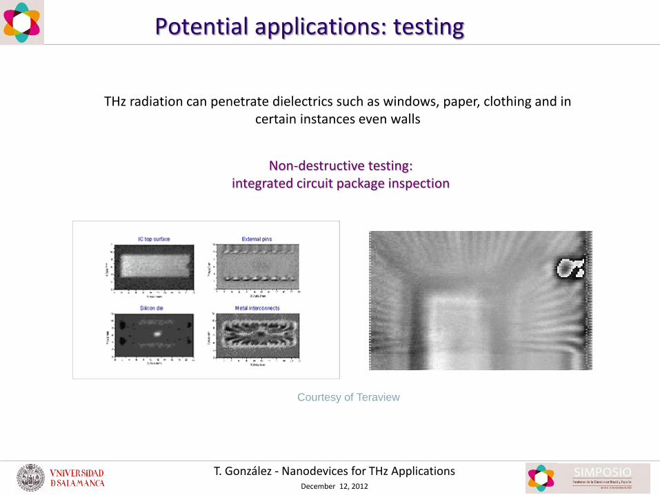
THz radiation can penetrate dielectrics such as windows, paper, clothing and in certain instances even walls
Potential applications: security
T. González - Nanodevices for THz Applications December 12, 2012
Non-destructive testing: integrated circuit package inspection
Courtesy of Teraview
THz radiation can penetrate dielectrics such as windows, paper, clothing and in certain instances even walls
Potential applications: testing

T. González - Nanodevices for THz Applications December 12, 2012
THz radiation can penetrate dielectrics such as windows, paper, clothing and in certain instances even walls
THz radiation can penetrate organic materials without ionizing
Weapon or Explosive Detection (metallic or non metallic)
Courtesy of Qinetiq Courtesy of Thruvision Courtesy of Qinetiq
Potential applications: security

T. González - Nanodevices for THz Applications December 12, 2012
THz radiation can penetrate dielectrics such as windows, paper, clothing and in certain instances even walls
Full-body security screening, body scanners
Potential applications: security
Passive Detection - no THz source is needed

T. González - Nanodevices for THz Applications December 12, 2012
THz radiation can be used to identify spectral fingerprints of explosives, narcotics, or active pharmaceutical ingredients
THz Spectroscopy
Potential applications: spectroscopy
Driving force of THz technology so far: spectroscopy, imaging, sensing
Active Detection - THz sources are needed (narrow or broadband)

T. González - Nanodevices for THz Applications December 12, 2012
Potential applications: communications

T. González - Nanodevices for THz Applications December 12, 2012
Evolving THz market

T. González - Nanodevices for THz Applications December 12, 2012
The THz gap
ELECTRONICS PHOTONICS THz Gap
All-optical sources
•Mixing lasers with close frequencies
•Excitation of semiconductors or
superconductors with fs laser pulses
•Quantum cascade lasers
All-electronic sources
• Gunn diodes + frequency multipliers (Schottky diodes)
Bulky and expensive equipment
Useful for spectroscopy and sensing, but not for communications
Very low power in the THz range
Backward wave oscillators - BWOs (vacuum electronic device)

T. González - Nanodevices for THz Applications December 12, 2012
The THz Gap
Quantum cascade lasers (QCL)
QCL at cryogenic T
Frequency multipliers
_ Other electronic devices: amplifiers, RTDs, IMPATT and Gunn diodes
500 GHz – 5 THz
Source: T. H. Crowe, W. L. Bishop, D. W. Porterfield, J. L. Hesler, and R. M. Weikle
“Opening the Terahertz Window with Integrated Diode Circuits”
IEEE J. Solid-State Circuits 40, 2104 (2005)
Signal generation at THz frequencies
PROBLEM Lack of a compact,
room-temperature, high-power, semiconductor
tunable source
Semiconductor Nanodevices for
Room Temperature THz
Emission and Detection
(ROOTHz Project)
The THz gap

T. González - Nanodevices for THz Applications December 12, 2012
Introduction. Importance of THz
ROOTHz Project
Self Switching Diodes (SSDs)
Conclusions / Perspectives
Outline
Outline
T. González - Nanodevices for THz Applications December 12, 2012
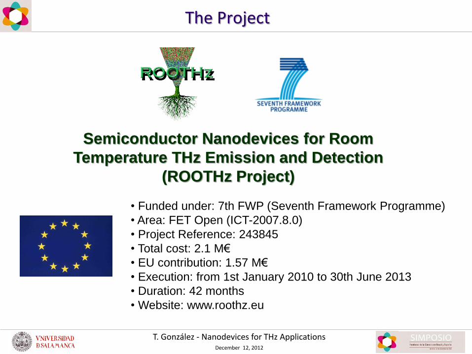
• Funded under: 7th FWP (Seventh Framework Programme)
• Area: FET Open (ICT-2007.8.0)
• Project Reference: 243845
• Total cost: 2.1 M€
• EU contribution: 1.57 M€
• Execution: from 1st January 2010 to 30th June 2013
• Duration: 42 months
• Website: www.roothz.eu
Semiconductor Nanodevices for Room
Temperature THz Emission and Detection
(ROOTHz Project)
The Project

T. González - Nanodevices for THz Applications December 12, 2012
C. Gaquiere
Institut d’Electronique Microélectronique
et de Nanotechnologie, Lille, France
A.M. Song
The University of Manchester
Manchester, UK
J. Grahn
Chalmers University of Technology
Gothenburg, Sweden
Coordinator: J. Mateos
University of Salamanca
Salamanca, Spain
Partners

T. González - Nanodevices for THz Applications December 12, 2012
Self Switching Diodes (SSDs)
Slot Diodes (Ungated HEMTs)
Barrier
Ohmic
Contact
Ohmic
Contact
Buffer
Channel
Cap LayerTop View
CurrentInsulating Trenches
Co
ntact
Co
ntact
Narrow Bandgap
Semiconductors (NBG):
InGaAs/AlInAs
InAs/AlSb
Wide Bandgap
Semiconductors (WBG):
GaN/AlGaN
Semiconductor nanodevices in ROOTHz
Final objective: fabrication of THz detectors and emitters with the same technology

T. González - Nanodevices for THz Applications December 12, 2012
Introduction. Importance of THz
ROOTHz Project
Self Switching Diodes (SSDs)
Conclusions / Perspectives
Outline
Outline
T. González - Nanodevices for THz Applications December 12, 2012
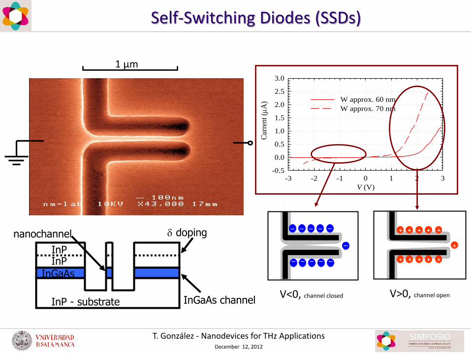
1 µm
V (V)
-3 -2 -1 0 1 2 3
Curr
ent
( A
)
-0.5
0.0
0.5
1.0
1.5
2.0
2.5
3.0
W approx. 60 nm
W approx. 70 nm
+
+ + + + +
+ + + + +
V>0, channel open
– – – – –
–
– – – – –
InP InP
InP - substrate
InGaAs
d doping
InGaAs channel
nanochannel
Self-Switching Diodes (SSDs)
V<0, channel closed

T. González - Nanodevices for THz Applications December 12, 2012
Adequate geometry for the onset of Gunn
oscillations
Tuneable threshold voltage from almost zero to more than
ten volts by adjusting the channel width
Simple technological process: etching of insulating trenches on a semiconductor
surface
Easy downscaling and parallelization: THz operation can be
obtained
Self-Switching Diodes (SSDs)

T. González - Nanodevices for THz Applications December 12, 2012
Self-Switching Diodes (SSDs)
• THz Detection: non-linear I-V characteristics
Use of NBG materials (Room Temperature ballistic transport) for increased
sensitivity and broadband
• THz Emission: Gunn Effect in InGaAs, and GaN !!
Use of WBG materials for increased power and frequency
• Planar geometry (and antennas) allow for a better coupling
• Parallelization for enhanced performances (and correct thermal management)

T. González - Nanodevices for THz Applications December 12, 2012
Introduction. Importance of THz
ROOTHz Project
Self Switching Diodes (SSDs)
Conclusions / Persp.
Outline
Outline
SSDs as THz detectors
SSDs as THz emitters

T. González - Nanodevices for THz Applications December 12, 2012
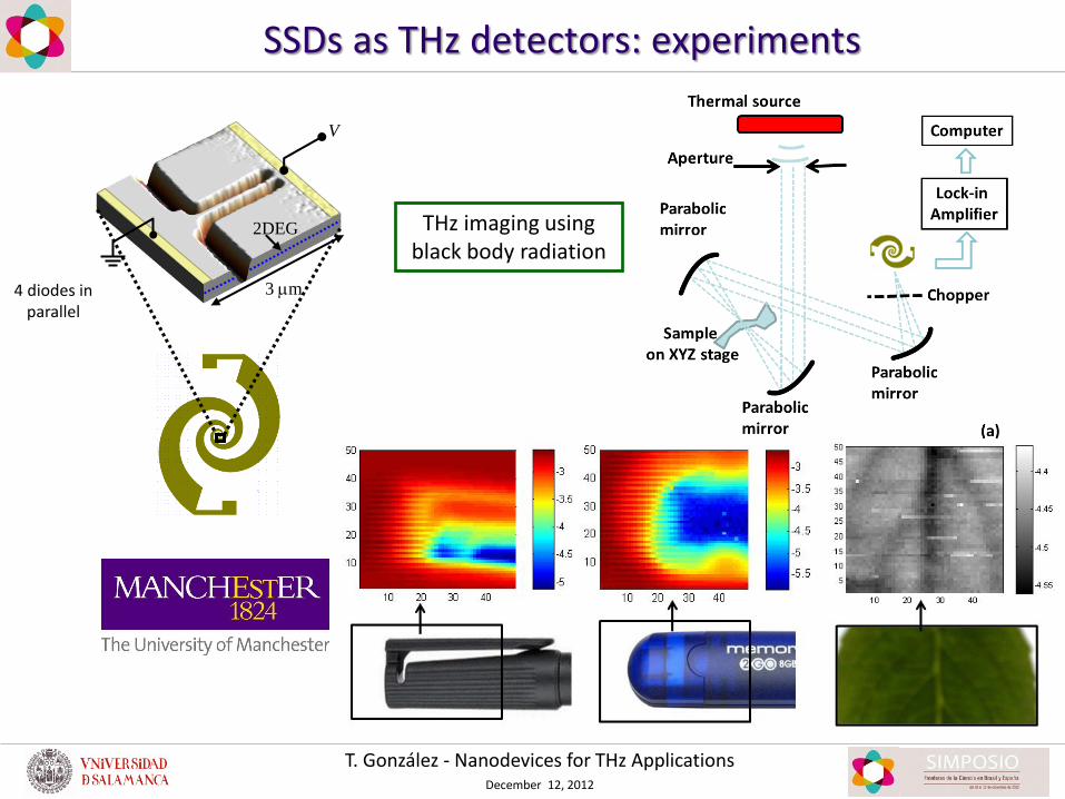
SSDs as THz detectors: experiments
3 m
2DEG
V
1 mm
C. Balocco et al., Appl. Phys. Lett. 98, 223501 (2011)
Room temperature
THz detection
4 diodes in
parallel -1.0 -0.5 0.0 0.5 1.0-4
0
4
8
12
16
20
Cu
rren
t (
A)
Voltage (V)
B
0.0 0.2 0.4 0.6 0.8-35
-30
-25
-20
-15
-10
-5
0
Outp
ut
DC
Voltage (
mV
)
Bias Current (A)
150 mV/mW
300 mV/mW T = 300 K
Responsivity
1330 V/W @ 12 K
Free Electron
Laser at 1.5 THz
T. González - Nanodevices for THz Applications December 12, 2012
3 m
2DEG
V
THz imaging using black body radiation
SSDs as THz detectors: experiments
4 diodes in parallel

T. González - Nanodevices for THz Applications December 12, 2012
600nm
Interdigital InGaAs mesa with 2000 etched SSDs
SSDs as THz detectors: experiments
• Corner frequency below 100 kHz even at relatively high biases
• NEP @ 110 GHz ~ 65 pW/Hz1/2 comparable to SBD
Noise can be reduced by increasing the number of SSDs in parallel
100m 1 10 100 1k 10k10
0
101
102
103
104
105
106
Vo
ltag
e n
ois
e (
nV
/Hz1
/2)
Frequency (Hz)
200 nA
300 nA
500 nA
1 A
2 A
no bias
1/f noise
T. González - Nanodevices for THz Applications December 12, 2012
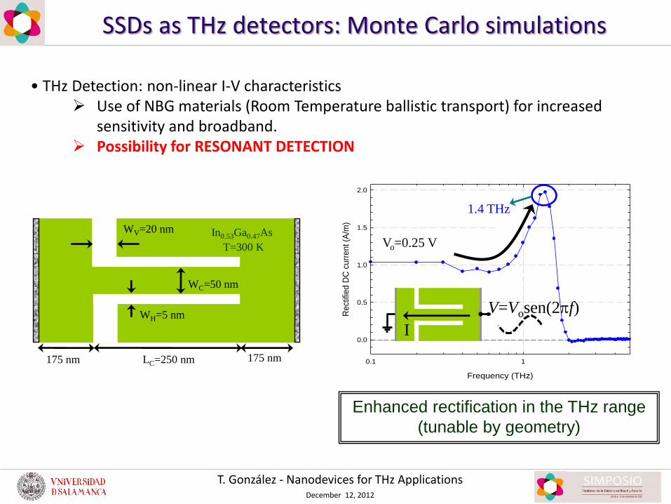
SSDs as THz detectors: Monte Carlo simulations
LC=250 nm
WC=50 nm
WV=20 nm
WH=5 nm
175 nm 175 nm
In0.53Ga0.47As
T=300 K
• THz Detection: non-linear I-V characteristics Use of NBG materials (Room Temperature ballistic transport) for increased
sensitivity and broadband. Possibility for RESONANT DETECTION
AC to DC
rectification
Frequency (THz)
0.1 1
Re
ctifi
ed
DC
cu
rre
nt (A
/m)
0.0
0.5
1.0
1.5
2.0
Vo=0.25 V
V=Vosen(2pf)
I
1.4 THz
Enhanced rectification in the THz range
(tunable by geometry)

T. González - Nanodevices for THz Applications December 12, 2012
THz dynamics in SSDs: pump-probe experiments
fs laser excitation beam 400 nm
Bias
Sampling beam 800 nm
Schematics of electro-optic (EO) sampling
EO crystal
Experiments done at Univ. of Rochester by Jie Zhang and Roman Sobolewski
T. González - Nanodevices for THz Applications December 12, 2012
Time (ps)
15 17 19 21 23
Curr
ent (A
/m)
-1000
0
1000
2000
3000
Exp
eri
me
nta
l (a
. u.)
-6
-4
-2
0
2
4
6
8
Experimental
V=1.0 V
V=-1.0 V
V=0.0 V
SSDs as THz detectors: pump-probe experiments
MC simulations predict a much sharper peak (1/3 FWHM), but the shape is similar
THz oscillations may be emitted from the excitation of the SSDs with fs-lasers
T. González - Nanodevices for THz Applications December 12, 2012
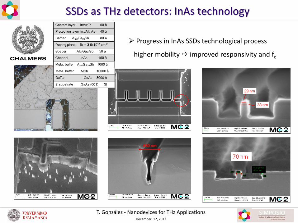
29 nm
38 nm
SSDs as THz detectors: InAs technology
Progress in InAs SSDs technological process
higher mobility improved responsivity and fc
650 nm
T. González - Nanodevices for THz Applications December 12, 2012
Introduction. Importance of THz
ROOTHz Project
Self Switching Diodes (SSDs)
Conclusions / Persp.
Outline
Outline
SSDs as THz detectors
SSDs as THz emitters

T. González - Nanodevices for THz Applications December 12, 2012
SSDs as THz emitters: Gunn oscillations
• Suitable geometry: vertical trench focuses
the electric field at the cathode side of the
channel, and anode voltage increases electron
concentration onset of domains and
propagation along the channel
Cointegration with detectors
• Material: GaN channels
High saturation velocity, low energy
relaxation time high frequency
High threshold field high power
Planar design SSDs in parallel
facilitates heat dissipation
(a)
(b)
n+ n- n n+

T. González - Nanodevices for THz Applications December 12, 2012
SSDs as THz emitters: Monte Carlo simulations
V (V)
25 30 35 40 45 50 55 60 65
Fre
quency
(G
Hz)
300
350
400
450 (b)
LC=900 nm
WC=75 nm
WV=100 nm
WH=50 nm
500 nm 150 nm
GaN T=300
K
Time (ps)
10 15 20 25 30 35 40 45 50
I (m
A)
0.4
0.8
1.2
1.6
2.0(a)
30 V
40 V
50 V
60 V
V (V)
-40 -20 0 20 40 60
I (m
A)
-0.2
0.0
0.2
0.4
0.6
0.8
1.0
Gunn
Oscillations
in GaN
SSDs
Monte Carlo Simulations
Oscillation frequencies above 400 GHz (voltage controlled and tunable by geometry)
T. González - Nanodevices for THz Applications December 12, 2012
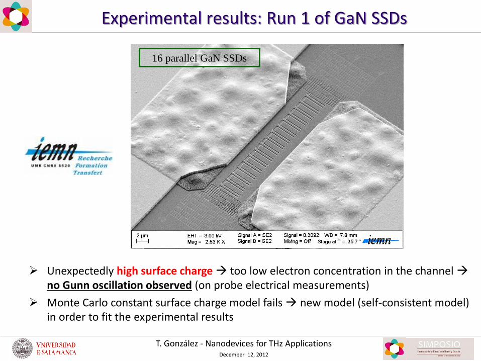
Unexpectedly high surface charge too low electron concentration in the channel no Gunn oscillation observed (on probe electrical measurements)
Monte Carlo constant surface charge model fails new model (self-consistent model) in order to fit the experimental results
Experimental results: Run 1 of GaN SSDs
16 parallel GaN SSDs

T. González - Nanodevices for THz Applications December 12, 2012
Bias (V)
-10 -5 0 5 10 15 20
Curr
ent (m
A)
-1.5
-1.0
-0.5
0.0
0.5
1.0
1.5
Experimental
MC
L= 500 nmW=500 nm
Bias (V)
-10 -5 0 5 10 15 20
L= 500 nmW=750 nm
Bias (V)
-10 -5 0 5 10 15 20
Curr
ent (m
A)
-1.5
-1.0
-0.5
0.0
0.5
1.0
1.5L= 500 nmW
in=350 nm
Wout
=450 nm
(a)
Experimental
MC
(b)
Experimental
MC
(c)
200 nm 450 nm L= 500 nm
50 nm
W=500 nm, 750 nm
100 nm
200 nm 450 nm L=500 nm
Win=350 nm
50 nm
100 nm (a) (b)
Wo
ut=4
50
nm
400 nm
400 nm
New strategies in the design
Experimental results: Run 2 of GaN SSDs
Wider square SSDs V-Shape SSDs
V-shape GaN SSDs
New Monte Carlo Self-consistent surface charge model GOOD AGREEMENT

T. González - Nanodevices for THz Applications December 12, 2012
Square SSDs: W ≥ 500 nm to provide Gunn oscillations (much wider that initially expected!!) VERY STRONG HEATING
V-shaped SSDs facilitate the onset of oscillations:
o Lower threshold voltage (30V instead of 50V in square SSDs) o Narrower channels are needed (W ≥ 200 nm)
Heating is much reduced with the V-shape
geometry
Experimental results: Run 2 of GaN SSDs
200 nm 450 nm L= 500 nm
50 nm
W=500 nm, 750 nm
100 nm
200 nm 450 nm L=500 nm
Win=350 nm
50 nm
100 nm (a) (b)
Wo
ut=4
50
nm
400 nm
400 nm
New strategies in the design
Wider square SSDs V-Shape SSDs
V-shape GaN SSDs

T. González - Nanodevices for THz Applications December 12, 2012
Free space measurements (devices with antenna mounted on PCB and Si lens)
In spite of large effort in characterization of emission in RF and THz no evidence of
oscillations were found in Run 2
Pulsed-mode measurements developed
Experimental results: Run 2 of GaN SSDs

T. González - Nanodevices for THz Applications December 12, 2012
Run 3 fabricated
Experimental results: Run 3 of GaN SSDs

T. González - Nanodevices for THz Applications December 12, 2012
1.8 mm
Z ~ 120 Ω
720 µm 4 µm
Bow-tie Emission not perpendicular
Z ~ 75 Ω
Equiangular spiral Emission perpendicular
Integration with adequately designed
broadband antennas
Experimental results: Run 3 of GaN SSDs

T. González - Nanodevices for THz Applications December 12, 2012
Good control of the technology
Experimental results: Run 3 of GaN SSDs

T. González - Nanodevices for THz Applications December 12, 2012
Structures designed for optimized heating
Higher bias can be applied (above the
threshold for the onset of oscillations)
No emission observed yet
Free-space characterization
Guided-wave characterization
under probes
Experimental results: Run 3 of GaN SSDs

T. González - Nanodevices for THz Applications December 12, 2012
Desynchronization of the oscillations: MC simulations
Single SSD
4-SSDs
2-SSDs
More SSDs in parallel, more pronounced desynchronization
An external resonator is needed for synchronization

T. González - Nanodevices for THz Applications December 12, 2012
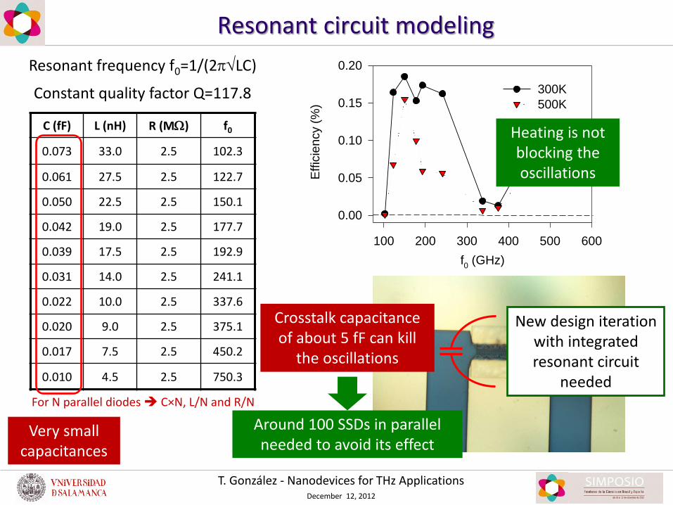
Resonant circuit modeling
• Series and parallel RLC circuits already implemented
• Circuit equations (solved in the time domain) coupled to the MC current
The voltage between terminals is fixed by the RLC circuit
T. González - Nanodevices for THz Applications December 12, 2012
Resonant circuit modeling
f0 (GHz)
100 200 300 400 500 600
Effic
ien
cy (
%)
0.00
0.05
0.10
0.15
0.20
300K
500KConstant quality factor Q=117.8
C (fF) L (nH) R (MW) f0
0.073 33.0 2.5 102.3
0.061 27.5 2.5 122.7
0.050 22.5 2.5 150.1
0.042 19.0 2.5 177.7
0.039 17.5 2.5 192.9
0.031 14.0 2.5 241.1
0.022 10.0 2.5 337.6
0.020 9.0 2.5 375.1
0.017 7.5 2.5 450.2
0.010 4.5 2.5 750.3
Resonant frequency f0=1/(2pLC)
Crosstalk capacitance of about 5 fF can kill
the oscillations
Around 100 SSDs in parallel needed to avoid its effect
Very small capacitances
Heating is not blocking the oscillations
New design iteration with integrated resonant circuit
needed For N parallel diodes C×N, L/N and R/N
T. González - Nanodevices for THz Applications December 12, 2012
Introduction. Importance of THz
ROOTHz Project
Self Switching Diodes (SSDs)
Conclusions / Perspectives
Outline
Outline
T. González - Nanodevices for THz Applications December 12, 2012
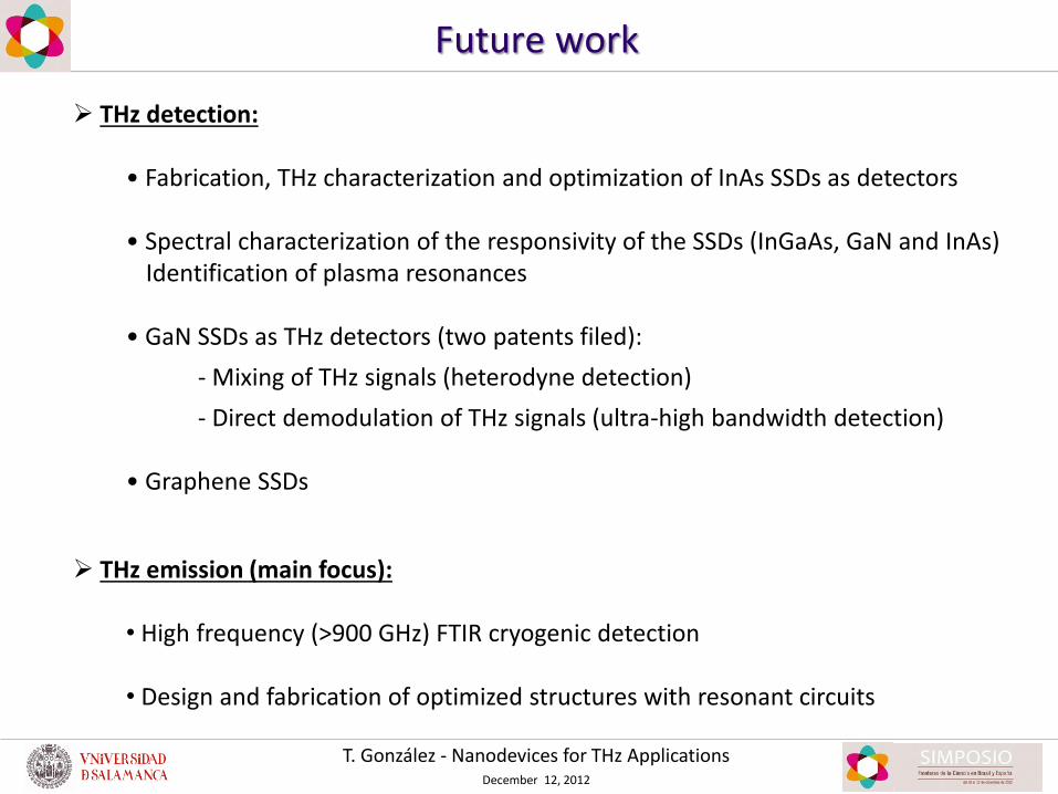
Future work
THz detection:
• Fabrication, THz characterization and optimization of InAs SSDs as detectors
• Spectral characterization of the responsivity of the SSDs (InGaAs, GaN and InAs) Identification of plasma resonances • GaN SSDs as THz detectors (two patents filed):
- Mixing of THz signals (heterodyne detection)
- Direct demodulation of THz signals (ultra-high bandwidth detection) • Graphene SSDs
THz emission (main focus):
• High frequency (>900 GHz) FTIR cryogenic detection • Design and fabrication of optimized structures with resonant circuits
T. González - Nanodevices for THz Applications December 12, 2012
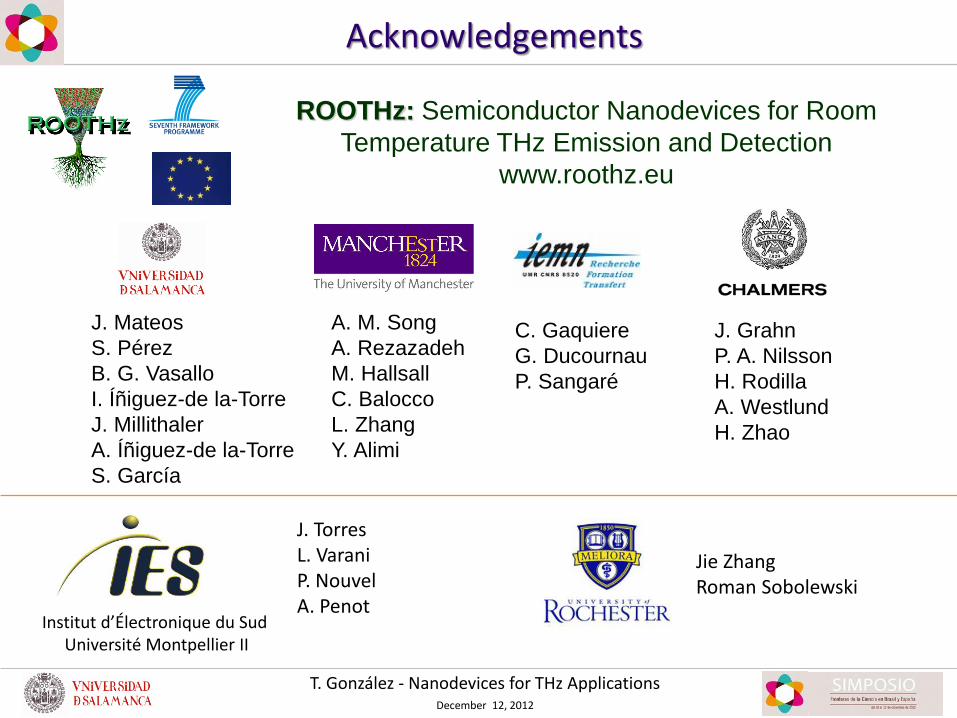
ROOTHz: Semiconductor Nanodevices for Room
Temperature THz Emission and Detection
www.roothz.eu
J. Mateos
S. Pérez
B. G. Vasallo
I. Íñiguez-de la-Torre
J. Millithaler
A. Íñiguez-de la-Torre
S. García
A. M. Song
A. Rezazadeh
M. Hallsall
C. Balocco
L. Zhang
Y. Alimi
C. Gaquiere
G. Ducournau
P. Sangaré
J. Grahn
P. A. Nilsson
H. Rodilla
A. Westlund
H. Zhao
Acknowledgements
Institut d’Électronique du Sud Université Montpellier II
J. Torres L. Varani P. Nouvel A. Penot
Jie Zhang Roman Sobolewski
T. González - Nanodevices for THz Applications December 12, 2012
Thanks for the attention !

T. González - Nanodevices for THz Applications December 12, 2012