universidad politÉcnica de madridoa.upm.es/47344/1/victor_jesus_gomez_hernandez.pdf · 2017. 7....
TRANSCRIPT

UNIVERSIDAD POLITEacuteCNICA DE
MADRID
ESCUELA TEacuteCNICA SUPERIOR DE INGENIEROS
DE TELECOMUNICACIOacuteN
ldquoEPITAXIAL GROWTH AND CHARACTERIZATION
OF INGAN LAYERS FOR PHOTOVOLTAICS
APPLICATIONSrdquo
DOCTORAL THESIS
Author
Viacutector Jesuacutes Goacutemez Hernaacutendez
Licenciado en Ciencias Fiacutesicas
2017
2
DEPARTAMENTO DE INGENIERIacuteA ELECTROacuteNICA
ESCUELA TEacuteCNICA SUPERIOR DE INGENIEROS DE
TELECOMUNICACIOacuteN
ldquoEPITAXIAL GROWTH AND CHARACTERIZATION
OF INGAN LAYERS FOR PHOTOVOLTAICS
APPLICATIONSrdquo
Author
Viacutector Jesuacutes Goacutemez Hernaacutendez
Licenciado en Ciencias Fiacutesicas
Thesis Supervisors Dr Miguel Aacutengel Saacutenchez Garciacutea
Dr Javier Grandal Quintana
2017
3
ldquoLos grandes palacios se construyen ladrillo a ladrillordquo
Viacutector J Goacutemez
4
Table of contents
Table of contents 4
Agradecimientos (Acknowledgements) 7
Abstract 9
Resumen 11
List of publications 13
As first author 13
As co-author 13
1 Introduction objectives and work plan 15
11 Introduction 15
111 The energy problem 15
112 Group III-Nitrides 17
113 Indium Gallium Nitride 19
12 Objectives 21
121 To check if the MME growth method may help in the development of an InGaN-based photovoltaic device 22
122 The study of the effect of four different buffer layers on the InGaN properties for InGaN on Si(111) photovoltaic devices 23
13 Work plan 25
131 Task 1 Systematic study of NID and Mg-doped GaN 25
132 Task 2 NID InGaN growth 25
133 Task 3 NID InGaN characterization 27
134 Task 4 growth and characterization of p-GaN i-InGaN n-GaN photovoltaic device using MME 27
14 Structure of the thesis 28
2 III-Nitrides properties 29
21 Structural properties of III-Nitrides 29
211 Crystalline structure 30
212 Polarity 34
213 Mechanical properties and strain 35
22 Structural defects 39
221 Point defects 39
222 Line defects 40
223 Planar defects 44
23 Band structure 46
5
231 Bandgap energy offset 48
232 Bandgap dependence with temperature and strain 50
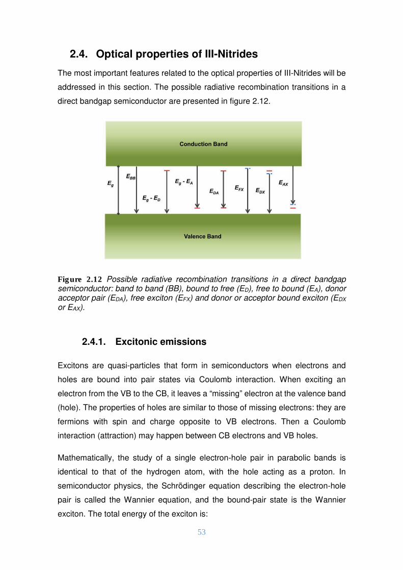
24 Optical properties of III-Nitrides 53
241 Excitonic emissions 53
242 Donor-Acceptor pairs 55
243 Mg- related emissions in doped III-Nitrides 56
244 Yellow Luminescence Band (YL) 58
245 Luminescence from basal stacking faults 59
246 UX1 and UX2 emission 60
25 Mg-doping of III-Nitrides 60
26 Polarization in III-Nitrides 62
261 Spontaneous polarization 62
262 Piezoelectric polarization 64
27 Specific properties of InGaN 66
271 Phase separation 66
272 Dependence of the structural parameters and bandgap with composition 69
3 Experimental techniques 71
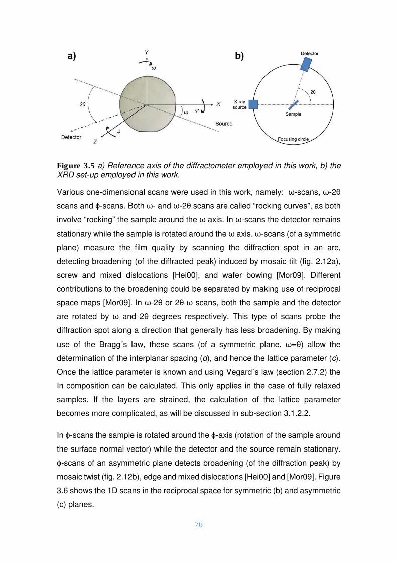
31 Structural characterization 71
311 Reflection High Energy Electron Diffraction (RHEED) 71
312 X-Ray Diffraction (XRD) 73
313 Transmission Electron Microscopy (TEM) 82
32 Morphological characterization 85
321 Atomic Force Microscopy (AFM) 85
322 Scanning Electron Microscopy (SEM) 86
33 Optical characterization 89
331 Photoluminescence (PL) 89
332 Cathodoluminescence (CL) 90
34 Electrical characterization 90
341 I-V measurements 90
342 Hall Effect 91
343 Solar cell characterization 95
35 Molecular Beam Epitaxy (MBE) 97
4 MME growth and characterization of Mg doped GaN layers on GaN(0001) on Sapphire templates 106
41 Introduction 106
42 Non-intentionally doped GaN grown on insulating templates for residual concentration analysis 107
6
43 Mg-doped GaN grown on insulating templates for hole concentration analysis 113
44 Conclusions 121
5 Metal Modulated Epitaxy (MME) growth and characterization of NID InGaN layers on GaN(0001)Sapphire templates 123
51 Introduction 123
52 Experimental procedure 123
53 IIIN ratio vs growth temperature diagram 125
531 Influence of the IIIN ratio 125
532 Influence of the substrate temperature 134
54 Control of the In content the InGa ratio 142
55 Effect of the shutters closing time 144
56 Growth of the p-i-n structure 148
561 Device results 150
57 Conclusions 156
6 Suitability of different buffer layers for InGaN-on-Si photovoltaic devices 158
61 Introduction 158
62 Experimental procedure 160
63 Results and discussion 162
631 Surface structure composition and morphology 162
632 Compositional uniformity 164
633 Crystallographic uniformity 166
634 Epitaxial relationship 167
635 Cathodoluminescence 169
636 Electrical characterization 171
64 Conclusions 173
7 Conclusions and future work 174
71 Conclusions 174
72 Future work 175
Appendix A Substrate preparation 178
Appendix B Device processing 179
References 182
7
Agradecimientos (Acknowledgements)
Hace seis antildeos comenceacute una andadura larga y complicada no exenta de
dificultades y aprendizaje llena de buenos amigos y amigas Muy lejos quedan
mis primeros diacuteas en el ISOM y aquella charlaentrevista con Enrique Calleja A
eacutel le que quiero agradecer la oportunidad que me dio para hacer el doctorado
dentro de uno de los grupos punteros de Espantildea
Durante todo este tiempo he tenido momentos de flaqueza momentos difiacuteciles
momentos en los que me planteeacute dejar el doctorado y la ciencia y dedicarme a
otra cosa En abril de 2015 mi salida era inminente En aquella eacutepoca Javier
Grandal se unioacute de nuevo al ISOM y se interesoacute por miacute y por mi trabajo Gracias
Javi por tu apoyo durante todo este tiempo y a hacerme ver que el esfuerzo
mereciacutea la pena que mi trabajo y yo eacuteramos importantes Gracias a eacutel decidiacute
continuar con la tesis pero no solo eso decidiacute continuar pensando que mereciacutea
la pena hacerlo Eacutel me ensentildeoacute a disfrutar de la ciencia del laboratorio de la
escritura cientiacuteficahellip
Queriacutea dar las gracias a Miguel Aacutengel por su empentildeo sus consejos y su
paciencia durante todo el tiempo que ha durado mi tesis con eacutel Tambieacuten quiero
agradecerle el haberme acogido como su alumno de doctorado cuando mi
anterior director de tesis se marchoacute de la universidad
Queriacutea agradecer a todos los que habeacuteis formado parte de estos antildeos de
doctorado Los doctores Praveen Kumar y Naveed Alvi con los que compartiacute
inumerables charlas sobre nuestras culturas y con los que paseacute muchas horas
de traacutemites con la administracioacuten A Pavel por las horas que hemos pasado
juntos hablando de ciencia de deporte de Espantildeahellip A Paul con quieacuten comparto
la pasioacuten del fuacutetbol Por aquellas tardes de FIFA de fuacutetbol sala de cervezashellip
Por todo el tiempo que hemos pasado juntos en el laboratorio y hemos discutido
resultados A Antonio un gran amigo por todas aquellas tardes en las que
hemos intercambiado ideas cientiacuteficas mientras tomaacutebamos una cerveza en el
parque Por todo el apoyo moral muacutetuo que nos hemos dado en los momentos
maacutes complicados Con quien comparto mi otra gran pasioacuten en la vida A Maika
nuestra querida teacutecnico del laboratorio le queriacutea dar las gracias por todo lo que
8
ha aportado a esta tesis pero queriacutea agradecerle por encima de todo lo gran
amiga que es Por los viajes que hemos hecho juntos por esas comidas donde
nos reiacuteamos a llorar por esas clases de conducir por esos grandes consejos
que me daba y que me ayudaban y me ayudan a mantener la cabeza friacutea en
momentos de corazoacuten calientehellip pero sobretodo por los momentos tanto
buenos como malos que hemos pasado juntos A mi amiga Sara a la que vereacute
maacutes a menudo en mi siguiente etapa cientiacutefica por esas charlas sobre nuestro
Atleacutetico de Madrid y sobre la apasionante saga de juego de tronos A todos los
compantildeeros y compantildeeras con los que he trabajado a lo largo de estos 6 antildeos
Ana B y Ana P Steven Zarko Patricia Amalia Alicia Oacutescar Fernando
MariMar Marco Ulloa Tommasso Gema Mariajohellip
A los que con su trabajo han colaborado para el desarrollo de este trabajo
Alejandro F Brantildea de Cal (ElySE) Mariacutea Varela del Arco (GFMC) y Fernando B
Naranjo y Araacutentzazu Nuacutentildeez Cascajero (GRIFO)
A mis amigos y hermanos Aacutelvaro y Roberto que siempre estuvieron ahiacute
daacutendome su apoyo incondicional tanto en los buenos como en los malos
momentos Por esas charlas en las que me preguntaacutebais ldquopero tuacute iquestQueacute es lo
que hacesrdquo Por esos viajes en los que mientras os echabais la siesta yo seguiacutea
preparando un congreso un artiacuteculo o la tesis A todos mis amigos del barrio del
voluntariado y a mi equipo de fuacutetbol
A mis padres que siempre me apoyaron en todas mis decisiones que me
ayudaron en todo lo posible y que me dieron toda su energiacutea cuando a mi me
faltaba A mi hermano Antonio con el que he compartido tanto y que me ha
apoyado en toda mi vida sobretodo en los momentos maacutes difiacuteciles Familia
gracias por todo os quiero
A Sara Has llegado en la recta final de esta maratoacuten y me has insuflado la
energiacutea necesaria para llevar este proyecto a buen puerto Te quiero
Por uacuteltimo a todos los que por error haya omitido de esta lista Muchas gracias
9
Abstract
In this work we have grown the constituent functional blocks of a photovoltaic
device based on III-Nitrides compound semiconductors focusing on the non-
intentionally doped (NID) InGaN layer and on the Mg-doped GaN layer We have
introduced two growth methods (MME and DERI) with the purpose of improving
the quality of those constituent blocks of a photovoltaic device All samples have
been grown in a molecular beam epitaxy (MBE) reactor
The Metal Modulated Epitaxy (MME) makes use of the modulation of the shutters
of the metallic and dopant sources (In Ga Al Mg Si) alternating open and close
conditions When the shutters are opened the growth is performed under metal-
rich conditions while when the shutters are closed it is performed under N-rich
conditions The main goal of the MME method is enhancing the proper
incorporation of Mg (p-type dopant) atoms into the crystalline structure (Mg atoms
on Ga substitutional site MgGa) while keeping a good morphology of the surface
Under N-rich conditions the Mg atoms are preferentially incorporated in MgGa
sites but the surface is degraded The surface is flattened back when growing
under metal-rich conditions The final result is an enhancement of the hole
concentration with a good surface morphology The overall growth conditions are
N-rich
Non-intentionally doped and magnesium doped GaN layers have been grown on
GaN(0001) pseudo-substrates by Metal Modulated Epitaxy (MME) In order to
characterize the hole concentration obtained the Mg-doped GaN layers were
also grown on highly resistive (GaNFe) pseudo-substrates MME The Hall effect
results have been compared with GaN layers grown in the intermediate regime
(the usual growth method by MBE for high quality layers) The layers grown by
MME showed 5 times higher hole concentration than those grown in the
intermediate regime The most important parameters to control the InGaN grown
on GaN(0001) pseudo-substrates by MME have been studied The ratio InGa
has been identified as the most critical parameter that controls the indium
incorporation into the alloy Diode p-i-n structures (p-GaN i-InGaN n-GaN) have
been grown on GaN(0001) pseudo-substrates processed and characterized and
crucial mechanisms have been identified in order to improve their performance
10
The other growth method used in this thesis is Droplet Elimination by Radical-
beam Irradiation (DERI) Unlike the MME case DERI growth of InGaN only
modulates openingclosing of the In shutter DERI consists of two process the
Metal Rich Growth Process (MRGP) and the Droplet Elimination Process (DEP)
During the MRGP the In shutter is opened and the layer is grown accumulating
In droplets on the surface When In shutter is closed (DEP) the In droplets are
reincorporated epitaxially into the InGaN layer The overall growth is
stoichiometric
In addition we have studied the effect of four different buffer layers on the
structural and optical properties of InGaN layers grown on Si(111) substrates and
their correlation with electrical characteristics The vertical electrical conduction
on the InGaN buffer Si with In composition near 46 which theoretically
produces a band alignment is analysed InGaN layers were grown for the first
time up to the best of our knowledge on Si using droplet elimination by radical-
beam irradiation (DERI) The results obtained lead to the possibility of fabricating
double junctions InGaNSi solar cells without the need of tunnel junctions
between the two sub-cells therefore simplifying the design of the final device
11
Resumen
En este trabajo hemos crecido los bloques funcionales que constituyen un
dispositivo fotovoltaico basado en la familia de semiconductores compuestos
conocidad como los nitruros centraacutendonos en las peliacuteculas de InGaN no
dopadas intencionadamente (NID) y las peliacuteculas de GaN dopadas con Mg
Hemos introducido dos meacutetodos de crecimiento (MME y DERI) con el objetivo de
mejorar la calidad de los bloques constituyentes mencionados para la fabricacioacuten
de un dispositivo fotovoltaico Todas las muestras se crecieron en un reactor
epitaxial de haces moleculares
El ldquoMetal Modulated Epitaxyrdquo (MME) hace uso de la modulacioacuten del estado de
los obturadores de metales y dopantes (In Ga Al Mg Si) alternando entre
abierto y cerrado Cuando los obturadores estaacuten abiertos el crecimiento se
realiza en condiciones ricas en metal mientras que cuando estaacuten cerrados se
realiza en condiciones ricas en nitroacutegeno El principal objetivo del MME es
aumentar la incorporacioacuten apropiada de los atomos de Mg en la estructura es
decir en posicioacuten de substitucional de Ga (MgGa) mientras que se mantiene una
buena morfologiacutea de la superficie En condiciones ricas en nitroacutegeno los aacutetomos
de Mg se incorporan preferentemente en posicioacuten de MgGa pero la superficie se
degrada Cuando las condiciones del crecimiento son ricas en metal
(obturadores abiertos) la superficie se planariza El resultado es un aumento de
la concentracioacuten de huecos en la capa de GaN con una morfologiacutea superficial
buena Globalmente las condiciones de crecimiento son ricas en nitroacutegeno
Se crecieron capas de GaN no dopadas intencionadamente sobre pseudo-
substratos de GaN(0001) por MME Se han crecido ademaacutes peliacuteculas de GaN
dopadas con Mg mediante MME sobre pseudo-substratos altamente resistivos
de GaN dopado con Fe Los resultados de las medidas de efecto Hall han sido
comparados con los de capas de GaN crecidas en reacutegimen intermedio (en este
reacutegimen se crecen las capas de mayor calidad) Las capas crecidas por MME
han mostrado una concentracioacuten de huecos 5 veces mayor que aquellas crecidas
en reacutegimen intermedio Tambieacuten se estudiaron los paraacutemetros maacutes importantes
que controlan el crecimiento del InGaN mediante MME sobre pseudo-substratos
de GaN(0001) Asimismo se identifica la razoacuten InGa como el paraacutemetro criacutetico
12
que regula la incorporacioacuten de indio en la aleacioacuten Para verificar el
comportamiento de las capas de InGaN se crecieron procesaron y
caracterizaron estructuras p-GaN i-InGaN n-GaN sobre pseudo-substratos de
GaN(0001) por MME y se identificaron mecanismos cruciales para mejorar su
funcionamiento
El ldquoDroplet Elimination by Radical-beam Irradiationrdquo (DERI) es el otro meacutetodo de
crecimiento basado tambieacuten en la modulacioacuten del estado de los obturadores que
se ha utilizado en esta tesis A diferencia del MME durante el crecimiento de
InGaN por DERI solo se modula el obturador de indio El DERI estaacute dividido en
dos procesos el ldquoMetal Rich Growth Processrdquo (MRGP) y el ldquoDroplet Elimination
Processrdquo (DEP) Durante el MRGP el obturador de In estaacute abierto y el crecimiento
de la capa se produce en condiciones de acumulacioacuten de gotas en la superficie
Cuando el obturador de In estaacute cerrado (DEP) las gotas de In se reincorporan en
la capa de InGaN Globalmente las condiciones de crecimiento son
estequiomeacutetricas
Hemos estudiado el efecto de cuatro capas de amortiguamiento diferentes sobre
las propiedades estructurales y oacutepticas de capas de InGaN crecidas sobre
Si(111) y su relacioacuten con las caracteriacutesticas eleacutectricas Se midioacute la conduccioacuten
vertical eleacutectrica de las hetero-estructuras InGaN ldquobufferrdquo Si para una
composicioacuten de In cercana al 46 que produce un alineamiento de bandas Se
crecieron por primera vez hasta donde llega nuestro conocimiento capas de
InGaN (~40 de In) sobre sustratos de Silicio utilizando eliminacioacuten de gotas por
irradiacioacuten con haz de radicales-libres (DERI) Los resultados obtenidos apuntan
a la posibilidad de fabricar ceacutelulas de doble unioacuten InGaNSi evitando la necesidad
de una unioacuten tuacutenel entre ambas sub-ceacutelulas simplificando el disentildeo del
dispositivo final
13
List of publications
As first author
1 High In Composition InGaN for InN Quantum Dot Intermediate Band Solar Cells V J Goacutemez P E D Soto-Rodriguez P Kumar E Calleja and R Noumltzel Jpn J of Appl Phys 52 08JH09 (2013)
2 Comparative study of single InGaN layers grown on Si (111) and GaN (0001) templates The role of surface wetting and epitaxial constraint V J Goacutemez Ž Gačević P E D Soto-Rodriacuteguez P Aseev R Noumltzel E Calleja and M A Saacutenchez-Garciacutea J of Crys Growth 447 48 (2016)
3 Study of the suitability of different buffer layers for InGaN-on-Si photovoltaic devices V J Goacutemez J Grandal A Nuacutentildeez-Cascajero FB Naranjo M Varela M A Saacutenchez-Garciacutea and E Calleja submitted to ACS Applied Materials and Interfaces
As co-author 1 A comprehensive diagram to grow (0001) InGaN alloys by molecular beam
epitaxy Ž Gačević V J Goacutemez N G Lepetit P E D Soto-Rodriacuteguez A Bengoechea S Fernaacutendez-Garrido R Noumltzel and E Calleja J Crys Growth 364 123 (2013)
2 Highly efficient potentiometric glucose biosensor based on functionalized
InN quantum dots N H Alvi P E D Soto-Rodriguez V J Goacutemez P Kumar G Amin O Nur M Willander and R Noumltzel Appl Phys Lett 101 153110 (2012)
3 Near-infrared InN quantum dots on high-In composition InGaN P E D
Soto-Rodriguez V J Goacutemez P Kumar E Calleja and R Noumltzel Appl Phys Lett 102 131909 (2013)
4 First Demonstration of Direct Growth of Planar High-In-Composition
InGaN Layers on Si P Kumar P E D Soto-Rodriguez V J Goacutemez N H Alvi E Calleja and R Noumltzel Appl Phys Express 6 035501 (2013)
5 An InNInGaN Quantum Dot Electrochemical Biosensor for Clinical
Diagnosis N H Alvi V J Goacutemez P E D Soto-Rodriguez P Kumar S Zaman M Willander and R Noumltzel Sensors 13 13917 (2013)
6 Spontaneous formation of InGaN nanowall network directly on Si P E D
Soto-Rodriguez P Kumar V J Goacutemez N H Alvi J M Maacutenuel F M Morales J J Jimenez R Garciacutea E Calleja and R Noumltzel Appl Phys Lett 102 173105 (2013)
7 Photoelectrochemical water splitting and hydrogen generation by a
spontaneously formed InGaN nanowall network N H Alvi P E D Soto-
14
Rodriguez P Kumar V J Goacutemez P Aseev A H Alvi M A Alvi M Willander and R Noumltzel Appl Phys Lett 104 223104 (2014)
8 Uniform Low-to-High In Composition InGaN Layers Grown on Si P Aseev P E D Soto-Rodriguez P Kumar V J Goacutemez J M Maacutenuel F M Morales J J Jimeacutenez R Garciacutea E Calleja and R Noumltzel Appl Phys Express 6 115503 (2013)
9 Highly Sensitive and Fast Anion-Selective InN Quantum Dot
Electrochemical Sensors N H Alvi P E D Soto-Rodriguez V J Goacutemez P Kumar M Willander and R Noumltzel Appl Phys Express 6 115201 (2013)
10 Stranski-Krastanov InNInGaN quantum dots grown directly on Si (111)
P E D Soto-Rodriguez P Aseev V J Goacutemez P Kumar N H Alvi E Calleja J M Maacutenuel F M Morales J J Jimeacutenez R Garciacutea A Senichev C Lienau and R Noumltzel Appl Phys Lett 106 023105 (2015)
11 Near-infrared emitting In-rich InGaN layers grown directly on Si Towards
the whole composition range P Aseev P E D Soto-Rodriguez V J Goacutemez J M Maacutenuel F M Morales J J Jimeacutenez R Garciacutea A Senichev C Lienau E Calleja and R Noumltzel Appl Phys Lett 106 072102 (2015)
12 InNInGaN Quantum Dot Photoelectrode Efficient Hydrogen Generation
by Water Splitting at Zero Voltage N H Alvi P E D Soto-Rodriguez P Aseev V J Goacutemez M Willander and R Noumltzel NanoEnergy 13 291 (2015)
13 Electrocatalytic oxidation enhancement at the surface of InGaN films and nanostructures grown directly on Si (111) P E D Soto-Rodriguez V Calderon P Aseev V J Goacutemez P Kumar N H Alvi A Saacutenchez R Villalonga J M Pingarroacuten and R Noumltzel Electrochem Comm 60 158 (2015)
15
1 Introduction objectives and work plan
11 Introduction
111 The energy problem
Solar energy is one of the most promising alternatives to reduce the current global
warming of the planet induced by greenhouse gases (GHG) arising from the use
of fossil fuels The potential of solar energy is much higher than that of the fossil
fuels or of any other renewable energy since the solar energy impinging on earth
in one hour is much higher than the worldwide energy expenditure in one year
There are two main technologies developed to harness the solar energy
i Solar thermal energy it harnesses the solar energy by heating a fluid
inside a circuit to produce steam which is then used to power a generator
that produces electricity This is an indirect transformation of sunlight into
electricity
ii Photovoltaic energy (PV) it converts solar energy directly into electricity
using a semiconducting material The semiconductor absorbs photons
from the sunlight generating electron-hole pairs Electrons and holes are
then separated inside the material by an internal electric field producing
an output voltage than can power a circuit This is a direct conversion of
light into electricity
These two ways of extracting energy from the sun are highly reliable safe and
easy to install needing relatively low operation and maintenance cost In addition
once installed none of them involves any combustion or GHG generation thus
making them environmentally friendly Therefore the development of high
efficiency and reduced cost solar cells is very desirable
The research in the field of PVs focuses mainly on the performance increment
while reducing the manufacturing costs
Nowadays more than 90 of the total solar panels produced worldwide are
made out of mono-crystalline silicon (Si) whose price reached 06euro per watt with
16
a 18 efficiency As an alternative panels based on low cost materials such as
amorphous silicon polycrystalline silicon and cadmium telluride have a slightly
smaller price (around 046euro per watt) However their shared market is low
because their efficiency hardly ever reached 16 The large density of defects in
the above-mentioned materials produces a dramatic reduction on the carriers
(electrons and holes) diffusion length and lifetime [Bha94] Higher efficiencies
close to 30 are only achievable in thin film III-V multi-junction (MJ) solar cells
such as GaInPGaInAsGe or GaInPGaInAsGaInAs These solar cells are
fabricated on germanium (Ge) or gallium arsenide (GaAs) substrates which are
more expensive than Si and all the junctions are designed to have a better
matching to the solar spectrum than with the above-mentioned technologies
leading to a higher efficiency
Nowadays single-junction Si solar cells with a reduced cost and long lifetime (30
years) monopolize the PV market despite their theoretical efficiency limit
(Shockley-Queisser) of 33 at the standard AM15G under 1 sun of illumination
(solar spectrum impinging the earth at a solar zenith angle of 4819deg) Using
advanced MJ solar cells based on III-V thin films higher efficiencies both under
1 sun and under concentration conditions (using lenses to mimic more than 1x
sun illumination) can be achieved Some designs showed efficiencies over 40
under concentration conditions using multilayers of arsenides phosphides and
antimonides on Ge substrates (447 for 4 junctions under a 297 suns
illumination) [Fra13] The main drawback of these types of MJ solar cells is their
higher price as compared with the silicon technology making them unsuitable for
a massive energy harvesting
Integration of the mature and relatively cheap Si technology with the efficient III-
V solar cells may allow the production of high efficiency and reduced-cost solar
cells Those structures would have a theoretical efficiency limit of 39 (for 1x
sun) and of 423 under concentration conditions (500x suns) [Kur90] It is worth
pointing out that those theoretical efficiency values could be achieved using a 2
junction solar cell composed by an upper cell with a bandgap energy of 174 eV
and a bottom cell with a bandgap energy of 113 eV [Kur90] Those bandgap
energy values could be obtained using a single semiconductor alloy system for
instance indium gallium nitride (InxGa1-xN) from the III-Nitrides system This
17
ternary compound semiconductor has been widely used for light emitting diodes
(LEDs) and laser diodes (LDs) during the last 20 years
112 Group III-Nitrides
Group III-Nitrides (AlN GaN and InN) have been considered a promising system
for semiconductor device applications since 1970 especially for the fabrication
of optoelectronic devices working in the ultraviolet to green range The III-Nitrides
(AlN GaN and InN) are optimal candidate materials for optoelectronic
applications at such photon energies because they provide a continuous alloy
system (InGaN InAlN and AlGaN) whose direct bandgap energies for the
hexagonal wurtzite structure range from 065 eV for InN 34 eV for GaN and 62
eV for AlN [Wu09] Likewise the strong ionic nature of their chemical bonding
gives them a high thermal and chemical stability making them suitable for
applications in aggressive environments and more specifically under strong
concentration conditions for PVs (high temperature operation) Other
advantageous properties include high mechanical stability high absorption
coefficient near the band edge (one order of magnitude larger than that of GaAs)
high carrier mobility large piezoelectric constants and the possibility of
passivation by forming thin layers of Ga2O3 or Al2O3 with bandgaps of
approximately 42 eV and 9 eV It is noteworthy as examples of devices that the
2014 Physics Nobel Prize was awarded to the development of light emitting
diodes (LED) with blue (1994) and ultraviolet (1997) emissions as well as UV
detectors and devices operating at high temperature [Nak95] Blue LDs based on
GaN are commercially available nowadays for Blu-ray disc players and white light
for car power headlights
To reach this state-of-the-art strong efforts were dedicated to the epitaxial growth
of prime quality material The main problem of the III-Nitrides is the lack of a
suitable material to be used as a substrate for homoepitaxial growth at a reduced
cost The main problems of using a foreign substrate (heteroepitaxial growth) are
the difference in thermal expansion coefficient and the difference in lattice
constant Consequently the epilayer grows with a large number of extended
defects (stacking faults [Lil08] [Glo08] dislocations [Kap95] [Lee01] [Chi96]
stacking mismatch boundaries [Sve96] [Smi95] and grain boundaries [Xu01])
18
Different substrates have been tested such as sapphire (Al2O3) silicon carbide
(SiC) and silicon (cut by the (111) planes)
In the 1970s Molecular Beam Epitaxy (MBE) and Metal Organic Vapour Phase
Epitaxy (MOVPE) growth techniques were developed and many efforts were
focused to make them capable of growing GaN However it was not until 1986
that high crystal quality GaN with good optical properties was produced by
MOVPE [Ama86] The breakthrough was the introduction of a thin (30 nm) layer
of polycrystalline AlN grown at low temperature (500ordmC) between the GaN layer
(grown at 1000ordmC) and the sapphire substrate This AlN interlayer (buffer layer)
helps to accommodate the difference in thermal expansion coefficient and lattice
constant During the heating process (from 500 to 1000ordmC) the AlN develops a
texture of small crystallites of preferential orientation (c-axis) on top of which GaN
grows The GaN layer starts with a high dislocation density that decreases rapidly
after growing a few microns A high quality surface was obtained a crucial factor
to grow thin multilayer structures in the following steps of the LED development
Shuji Nakamura at Nichia a chemical company in Japan developed a similar
method in which the AlN buffer was replaced by a low temperature GaN thin layer
[Ama86] [Nak91] A second major breakthrough was the achievement of p-type
conductivity in GaN layers which enabled the fabrication of GaN p-n junctions
[Nak91b] [Nak92] MOVPE was used by Nichia to develop the first blue and
ultraviolet LEDs (1994 and 1997 respectively)
In the case of GaN layers grown by MBE on Si(111) from the early 1994rsquos
[Ste94] studies focused on the use of AlN as buffer layers The best GaN layers
grown on Si(111) were achieved by using an AlN buffer [San98] [Hag02]
[Hag01] leading to the fabrication of optoelectronic devices [Guh96] [San00]
The first GaN-based ultraviolet (UV) photodetector grown on Si(111) by MBE was
demonstrated on 2000 [Pau00] Applications of III-Nitrides in PVs will be
mentioned in the next section
Heteroepitaxy of GaN on foreign substrates usually generates as mentioned
above a high density of dislocations grain boundaries inversion domains as
well as macroscopic defects (cracks) due to the difference in thermal expansion
coefficient (-33 and -17 vs sapphire and Si(111) respectively) and lattice
19
constant (-25 and 56 vs sapphire and Si(111) respectively) In spite of the
high concentration of defects devices with high efficiency have been produced
and are commercially available as LDs on ldquoBlu-ray Discrdquo players LEDs for indoor
and outdoor white light illumination traffic lights car lights displays and
televisions high power transistors and UV photodetectors For advanced devices
the defect density is reduced by buffer engineering or using high quality nitride
bulk substrates both prohibitive choices for mass production
113 Indium Gallium Nitride
Based solely on the III-Nitrides system (Al Ga In)N the bandgap can be tuned
from mid infrared (065 eV of InN) to UV (62 eV of AlN) Among ternary
compounds of this system a great deal of attention has been devoted to InGaN
alloys due to their application to green blue and UV LEDs and LDs Despite all
the resources invested to study and develop InGaN alloys some of their
fundamental properties remain somehow unclear For instance the presence and
nature of an electron surface accumulation layer the accuracy when determining
the actual bandgap carrier effective masses lattice parameters and elastics
constants some of them derived from a non-linear combination (bowing
parameter) of the corresponding values from the binaries GaN and InN
Nevertheless InxGa1minusxN alloys having a bandgap tuneable between 065 eV to
345 eV are excellent materials for optoelectronic applications This bandgap
energy span covers the entire AM15G solar spectrum InGaN films show an
exceptionally intense photoluminescence even though they are grown on lattice-
mismatched substrates In addition the optical and electronic properties of
InxGa1minusxN alloys exhibit a much higher resistance to high-energy (2 MeV) photon
irradiation than the currently used PV materials such as GaAs and GaInP
therefore offering a great potential for space applications Furthermore InxGa1minusxN
alloys have high temperature resistance making them suitable for solar cells
under concentration
As mentioned before the highest theoretical efficiency of a double junction solar
cell is attained when the bandgaps of the two sub-cells are 113 eV and 174 eV
both achievable by using InGaN Several approaches have been addressed
20
such as InGaN homojunctions and heterojunctions [Cai13] multi quantum wells
(MQWs) [Dah10] and InGaNGaN core-shell wires [Mes15] So far the record
efficiency reported for InGaN solar cells is established for a p-GaN i-InGaN-GaN
(MQWs) n-GaN solar cell at 595 [Lio11] and 599 [Lio13] both grown on a
buffered Si(111) substrate The most recent works done on InGaN solar cells are
focused on the design and simulation of the devices A p-InGaN i-InGaN n-
InGaN solar cells for an In content of 62 have been simulated by Jeon and co-
workers showing an efficiency of 3342 [Jeo16] The main problem associated
to the reports on simulations is that the structural parameters employed are
usually better than the state of the art An efficiency of 643 was reported by
Kushwaha et al for a simulated p-GaN i-InGaN n-GaN heterojunction solar cell
[Kus14] Huni et al reported on the simulation of a p-GaN i-InGaN (25) n-
GaN p-Si n-Si solar cell showing a photon conversion efficiency near 30
using a 4-terminal approach [Hun17] taking into account realistic and feasible
structural parameters Despite the attractive properties of InxGa1minusxN alloys
already described their growth remains challenging due to technological issues
that should be overcome
i At typical GaN growth temperatures (by MBE 750ordmC) the equilibrium
vapour pressure of InN is more than ten orders of magnitude higher than
that of GaN resulting in a very low In sticking coefficient The temperature
should be significantly reduced to ensure the incorporation of In into the
layer However low temperatures normally lead to In droplets formation
on the surface (InN dissociation temperature is much lower than the In
evaporation one) that also hinder In incorporation into the film In addition
at lower temperatures the InGaN crystal quality is much lower due to the
reduced surface mobility of the metal adatoms that generates rough
surfaces as well as extended and point defects
ii The large lattice mismatch between InN and GaN (11) results in highly
strained layers andor layers with a high density of dislocations
iii InGaN tends to separate into InN and GaN at temperatures typically over
500ordmC and In contents above 20 This phenomenon called phase
separation increases as a function of temperature and In content The
majority of III-V ternary and quaternary alloys are predicted to be
21
thermodynamically unstable and prone to phase separation and metal
clustering [Kar98] [Dop98] The growth by Molecular Beam Epitaxy (MBE
the growth technique employed throughout this work) is performed out of
the thermodynamic equilibrium conditions
iv The tendency of InGaN non-intentionally doped is to be highly n-type
doped due to point defects In addition there is an electron accumulation
layer at the surface that hinders p-type doping by pure compensation
[Vea06]
12 Objectives
The main goal of this thesis is to optimize the growth by MBE of nid InGaN layers
as well as their characterization aiming at their use for PV applications The
optimization of the growth involves the use of two new methods proposed in the
literature metal modulated epitaxy (MME) and droplet elimination by radical
beam irradiation (DERI) It also implies the understanding of the processes
related to the growth and the impact of individual parameters on the surface
morphology as well as on the structural optical and electrical properties
Specific goals of this thesis are
i To check if the MME growth method may help in the development of an
InGaN-based photovoltaic device
a The growth and characterization of non intentionally doped (NID)
and Mg-doped GaN on GaN(0001) templates by MME
b The growth and characterization of NID InGaN layers on
GaN(0001) templates by MME
c The growth and characterization of a p-GaN i-InGaN n-GaN
photovoltaic device using MME
ii To study the effect of four different buffer layers on the InGaN properties
for InGaN on Si(111) photovoltaic devices
a The growth and characterization of NID InGaN layers on buffered-
Si(111) by DERI
b The study of the effect of four different buffer layers on the InGaN
buffer p-Si vertical conduction
22
121 To check if the MME growth method may help in
the development of an InGaN-based photovoltaic
device
The wide range of band gap energies available from InGaN alloys combined with
other properties such as their absorption values make InGaN very attractive for
photovoltaic applications The structure selected to accomplish this goal was a p-
GaN i-InGaN n-GaN The large quantity of reports on growth and simulation of
this structures [Kus14] [Jeo16] [Hun17] together with the fact that the records
on InGaN-based solar cells have been obtained using those structures [Lio11]
[Lio13] make us to decide to use a p-GaN i-InGaN n-GaN over other options
This was selected over the InGaNMg InGaNSi one because the latter
introduces new technological problems that still need to be solved (as the Mg
doping of the InGaN layer) and that could screen the results on the growth
method The In content of the InGaN layer of the final device will be set to 10
to avoid problems related to the growth of high In content InGaN alloys This goal
was divided into three sub-goals
1211 The growth and characterization of non intentionally doped (NID) and Mg-doped GaN on GaN(0001) templates by MME
Full control of layers doping processes is a crucial step in the fabrication of any
optoelectronic device The doping study will follow the optimization of NID GaN
layers in which the residual doping will be determined Magnesium will be used
as the acceptor species for p-type doping Special emphasis will be put on the
use of the MME technique to grow Mg-doped GaN layers
Characterization (mostly structural optical and electrical) of the doped GaN
layers and a comparison with the results obtained on NID ones will result on a full
understanding of the issues related to the doping process
1212 Growth and characterization of NID InGaN layers on GaN(0001) templates by MME
Full control and reproducibility when growing InGaN alloys can be only achieved
by means of a deep understanding of the growth process For this purpose this
work addresses first the growth of NID InGaN layers It is fundamental to obtain
23
high crystalline quality layers in order to understand their basic
propertieslimitations and to allow designing the best strategy to achieve high
efficient devices
The crystal quality of the InGaN layers is assessed from a detailed study of the
morphological structural optical and electrical properties carried out by X-Ray
Diffraction (XRD) Transmission Electron Microscopy (TEM) Photoluminescence
spectroscopy (PL) Atomic Force Microscopy (AFM) and Hall Effect The results
are compared with the state of the art
1213 Growth and characterization of a p-GaN i-InGaN n-GaN photovoltaic device using MME
Prior to the design of a PV device a detailed study and analysis of the
heterostructures involved on its fabrication is necessary The final device will be
monolithically (ie all layers) grown by MBE The fabrication of the devices will
include several technological steps such as UV-lithography etching and metal
deposition of the electrical contacts
Additionally to the standard characterization of the layers a specific electrical
characterization of the resulting p-i-n junction and the measurement of the photo-
generated current in a solar simulator (conditions of AM15G under 1 sun
illumination) will be performed
122 The study of the effect of four different buffer
layers on the InGaN properties for InGaN on
Si(111) photovoltaic devices
The inability of a single-junction solar cell to harness the full solar spectrum gave
rise to the idea of stacking solar cells with different energy gap Theoretically the
maximum obtainable efficiency of a double-junction solar cell is 39 for a
bandgap combination of 174 and 113 eV Both values are achievable with
InGaN and Si An additional benefit of InGaNSi heterojunctions is the alignment
of the n-type InGaN conduction band with the valence band of p-type silicon for
In composition around 46 which provides a low resistance ohmic contact
[Hsu08] This fact would avoid the need of TJs between sub-cells strongly
24
simplifying the solar cell design and fabrication The bandgap of an In046Ga054N
is 18 eV and 111 eV for Si both values are close to the optimum ones In order
to accomplish this goal it was divided into two sub-goals
1231 The growth and characterization of NID InGaN layers on buffered-Si(111) by DERI
The growth of high quality high In content InGaN alloys on Si remains challenging
due to the large lattice mismatch between InN and GaN low miscibility gap and
the relatively low growth temperatures needed Additionally growing InGaN
alloys directly on Si must deal with the silicon surface nitridation and a poor
wetting on the resulting SixNy layer [Gom16] The silicon nitridation can be
avoided by using buffer layers that may in addition upgrade the film quality
DERI method can be of great help to grow high quality thick and homogeneous
NID InGaN layers with In content ranging from 30 to 42 The InGaN layers were
NID grown but the high residual n-type concentration was enough to ensure the
band alignment
The crystal quality of the InGaN layers is assessed in the same way as in the
case of InGaN grown by MME
1232 The study of the effect of four different buffer layers on the InGaN buffer p-Si vertical conduction
The vertical electrical conduction is going to be assessed by current versus
voltage (I vs V) characteristics The goal is to find a buffer layer that maximizes
the crystal quality of the InGaN epilayer while keeping the ohmic behaviour of
the n-InGaN buffer p-Si heterointerface
25
13 Work plan
A work plan has been established into different tasks aiming to accomplish the
specified goals
131 Task 1 Systematic study of NID and Mg-doped
GaN
The control of the doping level (p and n-type) is paramount for the fabrication of
devices In the case of III-Nitrides the n-type doping poses no significant
difficulties but for AlN and high Al AlGaN layers being commonly achieved by
using Si as dopant However p-type doping is still a serious challenge due mainly
to the high ionization energy of the acceptors commonly used that in AlGaN
layers increases with the mole fraction In addition compensation by donor
contamination (O Si) and point defects aside from the natural tendency of InGaN
layers to have a significant residual n-type character poses further difficulties
The presence of a high electron density at the layer surface for In mole fractions
beyond 50 [Vea06] adds even more difficulties to achieve effective hole
transport
In this work Mg was used as p-type dopant According to the literature MME
gives the best results in terms of hole concentration (426 x 1019 cm-3 for GaN
and 24x1019 cm-3 for In015Ga085N) mobility and crystal quality [Nam08] [Try09]
[Mos13] Therefore MME was the growth method selected to study the p-type
doping in GaNMg layers grown on semi-insulating (Fe-doped GaN)
GaNSapphire templates with emphasis on doping efficiency and on the effects
of Mg atomic incorporation on compensation effects polarity inversion and the
final hole concentrationmobility The results were compared with GaNMg layers
grown by conventional MBE on the same template type and with the state of the
art [Nam08] [Mos13] and [Gun15]
132 Task 2 NID InGaN growth
MBE is the technique to grow all III-Nitride layers studied in this thesis Given the
high complexity of the MBE system the first part of this task will focus on the
understanding and mastering all the needed knowledge to operate it
26
The substrate selection is critical to grow InGaN layers In this thesis both Si(111)
and commercial MOVPE GaNSapphire templates were used Each of them has
its own advantages and disadvantages For Si(111) different buffer layers are
needed to accommodate the lattice and thermal mismatch as well as the different
crystalline structure (Wurtzite and diamond) The effects of different buffer layers
grown on Si(111) on the resulting InGaN layers properties were studied namely
AlN InAlN both grown by MBE as well as sputtered InAlN and SiN produced by
direct nitridation of the bare Si(111) surface
Series of InGaN layers were grown to study the influence of growth temperature
and IIIV ratio on the layer properties The IIIV ratio refers to the relation between
the active nitrogen (N) flux and the metal fluxes
= +
A heating tantalum filament covered with a pyrolytic boron nitride (PBN) diffusor
(for homogeneity) heats up the substrate The growth temperature is measured
and controlled by a thermocouple located in close contact with the PBN diffusor
and connected to a temperature controller In addition an optical pyrometer is
used to measure the actual temperature on the substrate surface once its
emissivity has been set from a temperature calibration reference For Si(111) this
reference is taken from the transition temperature from the 7x7 to 1x1 surface
reconstructions (860ordmC [Suz93]) to adjust the emissivity so that the pyrometer
provides the actual substrate temperature For GaNSapphire templates surface
reconstruction changes are not easy to determine so that the calibration is
performed by measuring the time needed to desorb a given amount of Ga
(monolayers) deposited on the surface [Gal07] This process is generally
checked by looking at the RHEED intensity changes RHEED is also used to
characterize in-situ the surface morphology while growing
27
133 Task 3 NID InGaN characterization
The characterization of the grown layers provided essential information on
material properties and the influence of growth parameters on them allowing a
quick feedback to set the optimal growth conditions Characterization was aimed
at morphological structural optical and electrical properties
Structural characterization
Reflection high energy electron diffraction (RHEED)
X-Ray diffraction (XRD)
Transmission electron microscopy (TEM)
Morphological characterization
Scanning electron microscopy (SEM)
Atomic force microscopy (AFM)
Optical characterization
Photoluminescence (PL)
Cathodoluminescence (CL)
Absorption spectroscopy
Electrical characterization
I-V measurements
Hall Effect measurements
Chemical characterization
Electron Energy Loss Sspectroscopy (EELS)
I-V measurements will be of great importance on the characterization of the
vertical electrical conductivity of the n-InGaN buffer p-Si heterointerface
134 Task 4 growth and characterization of p-GaN i-
InGaN n-GaN photovoltaic device using MME
The design of efficient InGaN solar cells requires a deep understanding of the
previously commented tasks that provide feedback on limitations and
fundamental practical aspects to fabricate a real device Photovoltaic devices
based on p-GaN i-In010Ga090N n-GaN can be fabricated on n-type
GaN(0001)Sapphire templates by MBE once the previously commented tasks
28
are achieved The final device was processed at the ISOM facilities and
characterized in the solar simulator of the Electronics and Semiconductors Group
(ElySe) of the Autonoma University of Madrid
The most relevant parameters of a solar cell are the following
bull Open circuit voltage (Voc) being the maximum output voltage achievable under
open-circuit conditions (infinite load resistance)
bull Short circuit current (Isc) being the maximum output current delivered under
short-circuit conditions (zero load resistance)
bull Fill factor (FF) being the ratio of the maximum obtainable power to the product
of the open circuit voltage and short circuit current
14 Structure of the thesis
The 2nd chapter of this thesis is dedicated to the description of the most relevant
properties of the III-Nitrides Despite being discussed for the III-nitrides family of
materials it is focused on the GaN and InGaN
In the 3rd chapter the fundamental experimental techniques employed on this
work are described Those techniques have been used to evaluate the structural
optical electrical and chemical properties of the samples
The 4th chapter is devoted to the results obtained on NID and Mg-doped GaN
layers grown by MME and its comparison with NID and Mg-doped GaN layers
grown in the intermediate regime
The 5th chapter shows the results related to the growth of NID InGaN layers and
the growth of a p-i-n device In this chapter the characterization of the InGaN
layers and p-i-n devices is also dicussed
The 6th chapter is devoted to the growth of InGaN layers by DERI on Si(111) This
chapter also shows the growth of four different buffers on Si and their influence
on the InGaN properties and on the vertical electrical conduction
The conclusions of this thesis and the future work are discussed on the 7th
chapter
29
2 III-Nitrides properties
The most important structural optical and electrical properties together with the
band structure and the polarization fields of the binary and ternary nitrides are
addressed in this chapter The properties and elemental parameters of the binary
materials were usually measured from bulk crystals grown on foreign substrates
such as sapphire GaAs and Si or from self-assembled nanocolumns (NCs) or
QWs All of them are subjected to the effects of a high TDD strain or partial
relaxation Nowadays the development of III-Nitrides bulk crystal growth
techniques such as Na-flux hydride vapour phase epitaxy (HVPE) and
ammonothermal growth allows the production of high quality GaN and AlN bulk
crystals They allow the precise determination of the properties and elemental
parameters
21 Structural properties of III-Nitrides
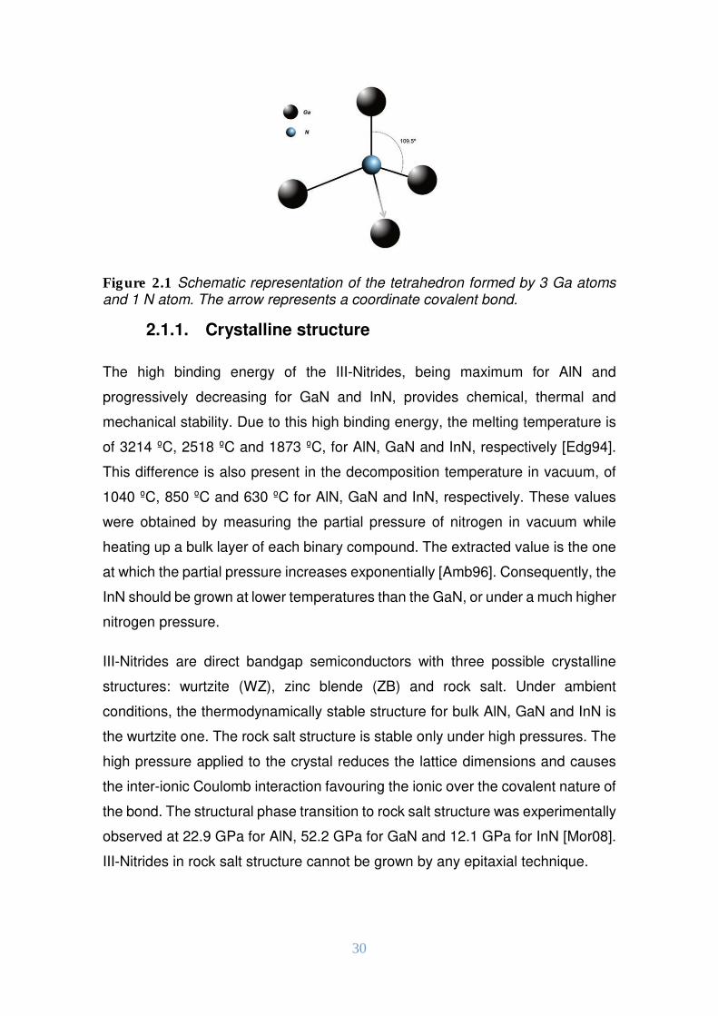
The electronic configuration of Ga and N atoms is
13 123434 12
Through a hybridization s and p orbitals form four sp hybrid orbitals with a
tetrahedron structure at 1095ordm In the case of Ga three of them are filled with
one electron and the fourth one is empty For N one is completed with two
electrons and the other three are filled only with one Then Ga and N atoms form
three covalent bonds and one coordinate (or dipolar) covalent bond formed
between the two electrons of one N bond and the empty sp orbital of the Ga atom
as shown in figure 21 Remember that every covalent bond has an ionic
character due to the difference in electronegativity between the constituent
atoms Only bonds between the same element are 100 covalent (N-N for
example)
30
Figure 21 Schematic representation of the tetrahedron formed by 3 Ga atoms and 1 N atom The arrow represents a coordinate covalent bond
211 Crystalline structure
The high binding energy of the III-Nitrides being maximum for AlN and
progressively decreasing for GaN and InN provides chemical thermal and
mechanical stability Due to this high binding energy the melting temperature is
of 3214 ordmC 2518 ordmC and 1873 ordmC for AlN GaN and InN respectively [Edg94]
This difference is also present in the decomposition temperature in vacuum of
1040 ordmC 850 ordmC and 630 ordmC for AlN GaN and InN respectively These values
were obtained by measuring the partial pressure of nitrogen in vacuum while
heating up a bulk layer of each binary compound The extracted value is the one
at which the partial pressure increases exponentially [Amb96] Consequently the
InN should be grown at lower temperatures than the GaN or under a much higher
nitrogen pressure
III-Nitrides are direct bandgap semiconductors with three possible crystalline
structures wurtzite (WZ) zinc blende (ZB) and rock salt Under ambient
conditions the thermodynamically stable structure for bulk AlN GaN and InN is
the wurtzite one The rock salt structure is stable only under high pressures The
high pressure applied to the crystal reduces the lattice dimensions and causes
the inter-ionic Coulomb interaction favouring the ionic over the covalent nature of
the bond The structural phase transition to rock salt structure was experimentally
observed at 229 GPa for AlN 522 GPa for GaN and 121 GPa for InN [Mor08]
III-Nitrides in rock salt structure cannot be grown by any epitaxial technique
31
The WZ structure has a hexagonal unit cell characterized by four lattice
constants three in-plane lattice constants (ai) and one out-of-plane (c) Only three
of them are independent two in plane and the one out of plane The wurtzite
structure consists of two interpenetrating hexagonal close packed (hcp) sub-
lattices each with one type of atom offset along the c-axis by 58 of the cell height
(5c8) and containing six atoms of each type
The ZB or cubic structure is stable when growing on cubic substrates such as Si
SiC MgO and GaAs where the substrate pushes the nitride to crystallize in a ZB
structure However the WZ structure can be present in the form of extended
defects (inclusions) In the ZB structure the position of the atoms within the unit
cell is identical to the diamond crystal structure consisting of two interpenetrating
face centred cubic sub-lattices offset by one quarter of the distance along a body
diagonal
In both structures WZ and ZB each atom may be viewed as positioned in the
centre of a tetrahedron with the four nearest neighbours located at the four
tetrahedron corners The main difference between both structures lies in the
stacking sequence of the atomic planes In WZ structure the stacking sequence
of the (0001) planes of Ga and N is hellipAaBbAaBbAahellip along the lt0001gt direction
while in ZB structure the staking sequence for the (111) close-packed planes is
hellipAaBbCcAaBbCchellip (Figure 22) Therefore when a change in the stacking
sequence occurs (stacking fault) inclusions of cubic-like material may appear in
a WZ structure and vice versa
Figure 22 Atomic arrangements of a) a wurtzite structure and b) a zinc blende structure
32
Figure 23 shows the spatial arrangement of the interatomic bonds of the two
neighbouring stacks (dashed line squares in figure 22) In WZ structure the
second neighbours of the two central atoms have symmetric positions (fig 23a)
while in the ZB structure they have inverted positions (fig 23b)
Figure 23 Spatial arrangements of the interatomic bonds in a) WZ and b) ZB lattices
In order to define the directions and the crystallographic planes in a WZ structure
Miller index nomenclature with four crystallographic axes is commonly used This
notation provides an intuitive and clear representation of the crystallographic
planes in hexagonal structures and allows the unit vectors to be perpendicular to
the respective planes With this notation crystal planes and directions are
expressed with Miller indices [ijkl] referred to the four unit vectors a1 a2 a3 and
c represented in figure 24 The Miller indexes are not independent to each other
they hold the relation + + = 0
Then if [UVW] are the indices referring to a triple axis reference system and
[uvtw] referred to a four-axis reference system the relation between both is given
by
= $ (2111) = 2 $ 3 (2112)
= amp $ (2113) amp = 2 $ 3 (2114)
33
= $ + amp( = $ + 3 (2115)
) = (2116) = ) (2117)
In the Miller notation the [100] direction is given by +2110- The planes
corresponding to the hexagonal prism faces are
100( 010( 110( 100( 010( and 110( for a three axis reference
corresponding to
1010( 0110( 1100( 1010( 0110( and 1100( in a four axis reference
It is easy to see that they are equivalent planes The most important crystal
planes in the WZ structure are the c-plane 0001 which is the most common
plane to grow on the non-polar m- 1-100 and a- 11-20 planes and the semi-
polar r-plane 1-102
Figure 24 Unit vectors represented on a hexagonal prism
34
212 Polarity
The most commonly used crystal plane to grow WZ GaN is the c-plane lt0001gt
The atoms are stacked in atomic bilayers with cations on one side and anions on
the other side The WZ structure is not centrosymmetric (no inversion symmetry
point) which results in polar faces and therefore two inequivalent growth
directions as shown in figure 25 Thus two polarities can be distinguished Ga-
polar (fig 25a) and N-polar (fig 25b) also referred to as Ga-face and N-face
Figure 25 Atomic arrangement in WZ GaN for a) Ga-polar and b) N-polar
Ga-polar corresponds to the +0001- direction in which Ga atoms are located on
top of the basal bilayer while the N-polar stands for the +0001- direction The
polarity is a bulk property that strongly depends on the growth method the
substrate used the way it is prepared and the growth conditions Ga-polar nitride
layers result when grown by MOVPE on Si-face 6H-SiC and on bare sapphire
High quality Ga-polar GaN layers result when grown by MBE on AlN buffered
sapphire and on silicon substrates while on bare wafers they present N-polarity
[Hel98] [Sum98] Brubaker and co-workers demonstrated that the growth
conditions also affects the polarity of the layer [Bru15] The polarity is established
at the very beginning of the growth during the deposition of the first bilayer and
35
it usually remains unchanged during the rest of the growth However polarity
could be locally inverted at structural defects such as inversion domains
stacking faults substrate surface steps or at different substrate surface
termination sites Only in such cases two different polarities could coexist in the
same epilayer
The two types of polarities Ga- and N-polar affect the growth kinetics and the
layer properties in a different way owing to the difference in the number of
dangling bonds (3 4 for Ga-polar and 1 1 4 for N-polar) A larger number of
dangling bonds (N-polar) reduces the ad-atom surface diffusion length during the
growth leading to rougher layers with lower chemical stability than the Ga-polar
ones In addition the formation energy of point defects and dislocations is lower
for the N-polar case Thus making the incorporation of impurities far easier for
the N-polar case as well as the formation of point defects and dislocations [Lil99]
[Pta00] [Pta01]
It is worth to mention that the layer termination and the layer polarity are different
concepts The layer termination is a property of the surface related to the atomic
reconstruction It does not depend on the layer polarity For instance a Ga-polar
layer could be N terminated under extreme N-rich conditions [Zyw98]
213 Mechanical properties and strain
The stress and strain present inside a continuous elastic material (such as a block
of rubber a piece of iron or a GaN layer) are connected by a linear relationship
that is mathematically similar to the Hookeacutes spring law
However the strain state in a solid medium around an arbitrary point cannot be
described by a single vector The same portion of material no matter how small
can be compressed stretched and sheared at the same time along different
directions Likewise the stresses in that material portion can be at once pushing
pulling and shearing
In order to reflect this complexity two second order tensors are required the
stress tensor (012) and the strain tensor (345) Their relation is given by
36
0 = 63 (2131)
Where c is the stiffness or elasticity tensor a fourth order tensor It could be
expressed also in the following form
3 = 0 (2132)
Where s is the compliance tensor the inverse of the elasticity tensor The
elasticity tensor is represented by a matrix of 3 x 3 x 3 x 3 = 81 real numbers
Then the Hookeacutes law holds that
012 = 7 7 61245345
58
48 = 1 2 3 (2133)
At a specific point of the material the strain tensor (ε) represents the displacement
of the particles in the neighbourhood of the point while the stress (σ) tensor
specifies the compression stretching or shearing forces that the particle is
suffering at that specific point The elasticity tensor (c) is a property of the material
and depends on temperature pressure microstructure and composition
Due to the inherent symmetries of the three tensors only 21 elastic coefficients
are independent For our case study the wurtzite structure there are 5
independent elastic constants Hence the relation between stress (012) and strain
(345) for a hexagonal crystal is given by the following equation
lt
0==0gtgt00gt0=0=gtAAB =
lt
C C C 0 0 0C C C 0 0 0C C C 0 0 00 0 0 CDD 0 00 0 0 0 CDD 00 0 0 0 0 C $ C2 AAAB E
lt
3==3gtgt323gt23=23=gtAAB (2134)
37
Only C11 C12 C13 C33 and C44 coefficients are independent
The difference in in-plane lattice constants between the epilayer (a) and the
substrate (a0) is the main source of strain in the epilayer that accommodates its
lattice constant to that of the substrate As a result the unit cell of the grown layer
is deformed (bond length and angle) and strain energy is building up as the
epilayer thickness increases Another source of strain refers to the difference in
thermal expansion coefficients Once the growth is finished upon the cooling
down process the substrate and the epilayer do not cool at the same rate and the
substrate forces the grown layer to follow its in-plane lattice change This strain
may be partially relaxed by the generation of dislocations resulting in a ldquoresidualrdquo
strain of thermal origin This is also the reason for having wafer or layer bowing
which is measurable in situ (during growth) by reflectometry
There are two types of deformation (i) when a gt a0 and the grown layer results
under in-plane biaxial compressive strain (fig 26a) or (ii) when a lt a0 and the
grown layer results under in-plane biaxial tensile strain (fig 26b) It is worth to
mention that an in-plane compression (tension) inevitably induces a uniaxial out-
of-plane tension (compression) along the c-axis (the volume of the unit cell
remains constant) The energy accumulated by strain is generally released
through the formation of dislocations which are very common in nitrides (to be
discussed in section 2221)
Figure 26 Schematic representation of lattice parameter accommodation between substrate and epilayer resulting in a) compressive biaxial strain and b) tensile biaxial strain
38
In the case of biaxial strain which preserves the hexagonal symmetry of the unit
cell the strain tensor is reduced to three independent components
3== = $ (2135)
3gtgt = F $ FF (2136)
3 = 6 $ 66 (2137)
Elastic constant (GPa) AlN GaN InN
C11 396 3594 223
C12 137 1292 115
C13 108 920 92
C33 373 3899 224
C44 106 980 48
Reference [Vur01] [Nakam12] [Vur01]
Table 21 Components of the elasticity tensor for AlN GaN and InN [Vur01]
Where a and b are the in-plane lattice constants and c is the out-of-plane lattice
constant of the strained epilayer and a0 b0 and c0 are the corresponding ones to
the substrate For wurtzite structures both in-plane lattice constants are equal
and thus 3== = 3gtgt The strain along the c-direction is not independent from the
in-plane one and is given by
39
3 = $2 CC 3== = $2 CC $ (2138)
The elasticity tensor coefficients are shown in table 21 for AlN GaN and InN
22 Structural defects
Crystalline solids are viewed as atomic periodic structures In ideal crystals the
atoms ions or molecules (hereafter only atoms) form the periodic crystal lattice
with fixed unit cell parameters However real crystals contain imperfections
known as crystallographic defects which locally disturb the regular arrangement
of the atoms breaking the perfect translational symmetry in the crystal which in
most cases generate electron (hole) states within the bandgap thus strongly
affecting the crystal properties These defects can be classified according to their
dimensional extension as point line planarsurface and bulkvolume defects
221 Point defects
Point defects are considered as zero dimensional ones with an extension of one
atom and limited to a given lattice site Point defects occur during growth doping
heating cooling plasma exposition and plastic deformation As native or intrinsic
defects point defects are most common in semiconductors having a strong effect
on their electrical and optical properties like carrier lifetime mobility radiative or
nonradiative recombination and compensation effects when doping The most
relevant point defects are interstitials (atoms incorporated at non-substitutional
lattice sites) vacancies (lack of an atom at a lattice site) and anti-sites
(exchanged anion-cation at a lattice site) As mentioned before point defects can
act as recombination centres which trap photo-generated carriers before they
reach a solar cell terminal thus reducing the carrier lifetime and its overall
efficiency A similar situation occurs for injected carriers in a LED or LD reducing
the internal quantum efficiency (IQE) of the device Further information on the
physics of point defects can be found in references [Zha91] [Wal96] [Wal04]
and [Sta00]
40
222 Line defects
2221 Dislocations
Linear or one-dimensional defects are those whose size in one dimension is
much higher than in the other two dimensions Dislocations for instance are
linear defects They represent the border of an unfinished plane in the crystal
Every dislocation is uniquely defined by its line of dislocation and its Burgers
vector The line of dislocation is the border delimiting a region of disorder within
the crystal and it can also be understood as the line of the longest dimension
The quantitative definition of a dislocation is given by the Burgers vector Its
atomistic definition is derived from the Burgers loop in the ideal and the deformed
crystal lattices The loop in the distorted crystal is a closed clockwise circulation
around the dislocation line as a chain of basis vectors of the lattice loop OPQMN
(figs 27a and b) The second Burgers loop is plotted on the ideal crystal ie
without a dislocation loop OPQMN (figs 27a and b) The difference between the
starting and ending point of both loops defines the Burgers vector (b) that
describes the magnitude and direction of the lattice distortion on figures 27c and
d FGH = IJGGGGGGH
Figure 27 Determination of the Burgers vector for a) c) an edge dislocation and b) d) a screw dislocation Image was adapted from [Kit76]
41
Every dislocation is uniquely defined by only one Burgers vector and it is
invariable in every point of the dislocation It implies that the dislocation cannot
start or terminate inside the crystal because then b would vary from 0 to any
specific value It could only start or terminate at the crystal surface the interface
with another crystal or on another defect or dislocation
Depending on the angle (φ) between the dislocation line and the Burgers vector
dislocations can be classified in the following way
bull When φ = 90ordm edge dislocation Figure 27a shows a pure edge dislocation
visualized as being caused by the abrupt termination of an atomic plane
inside the crystal In this case the surrounding planes are bent around the
dislocation line being the crystal structure perfectly ordered on either side
bull When φ = 0ordm screw dislocation Figure 27b shows a pure screw
dislocation In order to visualize a screw dislocation let us consider a cut of
the crystal along a plane and a slip of one half across the other by a lattice
vector when the halves fit back together without leaving a defect If the cut
only goes part of the way through the crystal and then slip the boundary of
the cut is a screw dislocation It comprises a structure in which a helical path
is traced around the dislocation line by the atomic planes in the crystal lattice
bull When 0ordm lt φ lt 90ordm the defect is called a mixed dislocation and can be
decomposed into pure edge and screw dislocations components
Dislocations can move under external applied stress giving rise to the following
type of movements
bull Glide or conservative motion when the dislocation moves in the plane which
contains both its line and Burgers vector A dislocation able to move in this
way is named glissile and those moving differently are called sessile
bull Dislocation motion by climb occurs when it moves out of the glide plane and
thus normal to the Burgers vector
Threading dislocations (TDs) are those with a dislocation line perpendicular to
the sample surface [Mor09] In III-Nitrides TDs occur usually along the [0001]
direction such as the c-plane GaN GaN layers grown on sapphire have TDs
densities (TDDs) in the range of 108-1010 cm-2 for standard growth and 106 - 107
42
cm-2 for epitaxial lateral overgrowth method (ELOG) [Muk03] [Det01] while for
bulk GaN (grown by HVPE ammonothermal method Na-flux) TDD can be
reduced down to 104 cm-2
As line defects TDs may have screw edge and mixed nature Screw dislocations
have the dislocation line parallel to the c-axis and the Burgers vector In general
mixed TDs are decomposed into pure screw and edge TDs and therefore will not
be specifically considered in this work Both edge and screw TDs nucleate in the
early stages of the growth and they thread to the crystallites surface therefore
most likely arising from islands merging during growth When the elastic energy
is accumulated in an epilayer it might be partially released by dislocation
formation The inhomogeneous strain field induced by the dislocation may lead
to surface roughening by changes induced in the growth regime Dislocations can
attract point defects (gettering process) like $ K( and $ K (deep
acceptors) and become electrically active [Els98] Screw dislocations are
electrically active and may act as non-radiative recombination centres [Els97]
Mixed dislocations with a screw component act also as non-radiative
recombination centres [Ros97] The ideal TDs are charged lines that mostly affect
mobility
TDs may also act as conducting pathways in Schottky barriers and LEDs leading
to increased leakage currents that may eventually result in device short circuit
[Hsu01] In general a high dislocation density of any type has a detrimental
influence on the device performance reducing the efficiency in charge transport
IQE and electrical noise being still a major technological challenge
To study misfit dislocations (MDs) some concepts should be first introduced The
relative difference between the in-plane lattice parameter of the relaxed substrate
(LMN5) and the one of the relaxed epilayer (NMN5) is called lattice mismatch (see fig
28a)
∆MN5LMN5 = NMN5 $ LMN5LMN5 (2221)
43
Lattice mismatch gives rise to elastic strain and changes elastically the lattice
parameter of the grown layer until relaxation (plastic) occurs The difference
between the strained lattice parameter of the epitaxial layer and the relaxed lattice
parameter of the substrate is called lattice misfit (fig 28b)
∆LPMLMN5 = NLPM $ LMN5LMN5 (2222)
Figure 28 a) Relaxed lattice parameters of epilayer and substrate b) heteroepitaxial system with misfit dislocation formation and c) MDs network in a heteroepitaxial system
Strain can be relaxed by the formation of surface undulations 3D islands and
MDs (fig 218c) The first two mechanisms take place at the initial stage of the
growth while the latter is dominant for thicker layers In principle MDs are not
supposed to thread up the epilayer and are very efficient in releasing strain
However TDs can be interconnected to the MDs network [Keh01]
44
223 Planar defects
Planar or two-dimensional defects are interfaces between homogeneous regions
of the material that include surfaces interfaces grain boundaries twin
boundaries and stacking faults
A real crystal has a finite size and thus surfaces The surface is the interface
between the crystal and the surrounding media (usually air) The surface has a
certain energy formation and a certain strain component (like in the case of a
spherical liquid droplet)
2231 Grain boundaries
The heteroepitaxy of III-Nitrides on highly mismatched substrates (such as InGaN
on Si) leads to the formation of isolated micro crystallites at the early stages of
the growth that tend to coalesce as the growth evolves and grains form by energy
minimization Differences in grain orientation can arise from an inhomogeneous
substrate or crystallite nucleation leading to either an inclination of the c-axis
between different grains named tilt (fig 29a) or a rotation of the basal plane
between different grains around the c-axis named twist (fig 29b)
Figure 29 Schematic representations of the micro crystallites of an epilayer when a) tilt and b) twist is presented
In the case of tilted grains a network of screw dislocations forms at the
boundaries between them while for the twisted grains a network of edge
dislocations appear at grain boundaries This can only be applied to low angle
grain boundaries
45
2232 Staking faults
Stacking faults appear in III-Nitrides as alterations of the stacking sequence of
Ga and N atomic planes along the (0001) direction The stacking sequence for a
WZ structure is AaBbAaBbAa and its modification may lead to
AaBbCcBbCcBbCc or AaBbCcAaBbCc sequences resulting in ZB inclusions
From another viewpoint stacking faults may be regarded as ldquoQuantum Dotsrdquo of
cubic material within a hexagonal matrix thus having strong emission properties
There are three different types of stacking faults
Type 1 (I1) contains one violation of the stacking rule of the Wz structure
AaBbAaBbCcBbCcBbhellip
Type 2 (I2) contains two violations of the stacking rule of the Wz structure
AaBbAaBbCcAaCcAahellip
Extrinsic (E) BSFs have an additional Cc layer inserted on the midst of the Wz
stacking sequence AaBbCcAaBbAaBbAahellip
Type 3 BSFs are not going to be considered in this work because it is intrinsic on
the ZB stacking sequence and not on the Wz one For a deeper insight the reader
is referred to [Sta98] and [Lah14]
The coalescence of islands with different stacking order leads to the formation of
complex planar defects stacking mismatch boundaries (SMBs) and inversion
domain boundaries (IDBs) These are typically flat and parallel to the [0001]
direction starting at the substrate surface and running through the entire
thickness of the epilayer In SMBs the stacking sequence is altered across the
boundary whereas at IDBs the occupation of the Ga and N sub-lattices is
reversed so that the polarity changes across the boundary
46
23 Band structure
III-Nitrides are direct bandgap semiconductors with the conduction band (CB)
minimum and the valence band (VB) maximum located at the centre of the
Brillouin zone QΓ point ℎXYX GH = 0Z In addition a high excitonic binding energy
and wide spectral range covered by ternary alloys are major advantages that
make them optimal candidates for optoelectronic applications
While in most ZB semiconductors the VB is degenerate the case of III-Nitrides is
different In III-Nitrides the hexagonal symmetry of the unit cell together with the
ionic character of the Ga-N chemical bond generates an asymmetry in the local
electric field and a VB splitting (known as crystal field splitting) into two sub-
bands one non-degenerate Γ state and two degenerated Γ states Additionally
the spin-orbit interaction ∆[( breaks the symmetry of the Γ states splitting them
into two non-degenerate sub-bands Figure 210 illustrates the case of WZ GaN
Thus the VB is split into three sub-bands the heavy hole (HH) the light hole (LH)
and the crystal-field split-off hole (CH) The energies of the valence sub-bands
HH (Γ]) LH (Γ) and CH (Γ) are given by Chuang and Chang [Chu97]
^_ ` = ^_ + ∆ab + 1 3 ∆[ (2301)
^_c`a` = ^_ + ∆ab $ 1 3 ∆[2 plusmn 12 ef∆ab + 1 3 ∆[2 g + 2 9 ∆[ (2302)
Where ^_ is a reference VB energy which can be set to zero ∆ab is the crystal
field splitting and ∆[ stands for the spin-orbit splitting Even though both splittings
cannot be directly measured they can be indirectly estimated from
photoluminescence and photorreflectance measurements of the free excitons A
B and C (excitons involving the three valence bands) as the energy difference
between the valence band levels
47
^_ ` $ ^_c`a` = ∆ab + ∆[2 ∓ 12 j∆ab + ∆[( $ 8 3 ∆[∆ab (2303)
The CB energy for GaN can be written as
^a = ^_ ` + l = ^_ + ∆ab + 1 3 ∆[ + l (2304)
Concerning the effective masses the symmetry of the unit cell in III-Nitrides with
ZB structure allows a parabolic approximation of the VB and CB following the
expressions
^ ( = ^ plusmn ℏ2ℏ ^ = ^ plusmn ℏ2nlowast (2305)
Where m stands for the effective mass of electrons and holes which in this
particular case are isotropic for the three spatial directions However III-Nitrides
with hexagonal structure present different energy band profiles for the in-plane
directions (x-y) that yield different values for the effective mass m|| parallel to the
growth plane and mperp for the z direction The effective mass approximation which
is now more strictly constrained to the GH = 0 proximity gives
^ ( = ^ plusmn ℏ2 p nqlowast + = + gtn∥lowast s (2306)
Thus two effective masses for electrons and two for holes in each VB (up to six)
can be defined in WZ nitrides Table 23 summarizes the values of various crystal
parameters
48
Figure 210 a) Schematic representation of the effect of the crystal field and spin-orbit interaction on the valence band maximum b) Band diagram of GaN The three valence sub-bands are represented as heavy holes (HH) light holes (LH) and crystal holes (CH) [Chu96]
231 Bandgap energy offset
When fabricating a device layers of different materials are grown upon each
other (stack) The knowledge of the band offsets is important to determine the
potential confinement properties in MQWs and heterojunctions
An energy offset (^tuu) is used to align the bandgaps of different materials In this
thesis GaN is chosen as the reference value for III-Nitrides (^tuu = 0 X) Then
the energies of the CB and VB edges can be written as
^_ = ^tuu (2311)
^a = ^_ + l = ^tuu + l (2312)
The VB-offset of AlNGaN (^tuuv5) heterojunction is taken as 112 eV which
corresponds to 40 of the total bandgap difference between the binaries
49
[Wes06] This determination was obtained from a measurement of the linewidth
of the excitonic transition in an Al018Ga082N alloy This value is larger than the
previously reported 07 eV in [Mar96] that was estimated by x-ray photoemission
spectroscopy However the latter is closer to the real value as it is free from
effects introduced by interface defects and other type of inhomogeneities
The most widely cited value for the VB offset of InNGaN heterojunctions is that
reported by Martin et al [Mar96] (^tuu = 105 X) over twenty years ago More
recent studies give values between 058 [Kin08] and 062 eV [Mos10] The band
alignments between the three binaries are shown in figure 211
For ternary alloys the VB offset energy is often calculated from [Pal04]
^tuu = ^tuuQ l $ lZ $ ^tuuQ l $ lZl $ l (2313)
Figure 211 Band alignment between the III-Nitride binaries
50
232 Bandgap dependence with temperature and strain
Any variation induced on the bond length will lead to changes of the band
structure and thus on the bandgap of the semiconductor This sub-section will
focus on the influence of the temperature and strain on the bandgap value
When the temperature increases the crystal lattice expands and the atomic
oscillations around their equilibrium lattice site increase A larger atomic
separation leads to lower bandgap energy This dependence is given by the
empirical expression developed by Varshni [Var67]
ly( = l0( $ zyy + | (2321)
Where l0( is the bandgap energy at 0 K z is an empiric constant and | is the
Debyeacutes temperature Values of these parameters are given in table 23
This expression fits relatively well for unstrained layers However for strained
layers Vashniacutes equation is not appropriate and a more accurate description
should be introduced The expression proposed by Fan [Fan51] agrees better
with the experimental data for strained layers
ly( = l0( $ X~ $ 1 (2322)
Where is a constant related to the average photon-phonon interaction and the is the Einsteinacutes temperature
The PL emission energies related to free excitons follow quite accurately the
bandgap temperature dependence given by Fanacutes and Varshniacutes equations A
similar behaviour is found for transitions associated with impurity states either
donors or acceptors (free-to-bound) for temperatures above the carrier freeze-
out into the impurity states (neutral donors or acceptors)
51
The influence of the strain on the bandgap can be quantified from a second order
perturbation model based on a kp method [Chu97] In the strained layer the VB
states are modified as
^_ ` = ^_ + Δab + 1 3 Δ[ + θ + λ (2323)
^_c`a` = ^_ + ∆ab $ 1 3 ∆[2 + 12 θ + λ plusmn 12 ef∆ab + 1 3 ∆[ + θ2 g + 2 9 ∆[ (2324)
Where θε and λε stand for
θε = Dε + DDQε + εZ (2325)
λε = Dε + DQε + εZ (2326)
And DD are hydrostatic deformation potential constants affecting the
transitions between the CB and VBs and DDD are uniaxial deformation
potentials that characterize the splitting of the VB in the presence of strain
perpendicular to the [0001] direction (DD) and along the [0001] direction (D)
Now the CB states are given by
^aY( = ^_ `Y( + l + ∥ε + qQε + εZ (2327)
Where ∥ and q are the deformation potentials of the epilayer for the out-of-
plane and in-plane directions The change in energy bandgap is then
∆ lY( = 23== +q $ $ D- $ CC +∥ $ $ - (2327)
52
Despite huge efforts to simulate and measure the mentioned material basic
parameters there is a strong dispersion and even contradictory results in the
literature mostly due to poor quality material and differences in strain arising from
specific heteroepitaxial growth techniques Table 22 summarizes the values of
these parameters
AlN GaN InN AlN GaN InN
Δab+X- -164 19 41
Electrons
n∥lowast n 028 02 012
Δ[+X- 19 14 1 nqlowast n 032 02 012
∥+X- -90 -65 -35
HH
n∥lowast n 204 127 156
q+X- -90 -118 -35 nqlowast n 208 102 125
+X- -30 -30 -30
LH
n∥lowast n 204 127 156
+X- 36 36 36 nqlowast n 020 011 009
+X- 96 882 882
CH
n∥lowast n 024 204 204
D+X- -48 -441 -441 nqlowast n 204 014 012
+X - 18x10-3 77x10-4 245x10-4 |+- 1462 600 624
Table 22 Values of the crystal field and spin-orbit splitting deformation potentials effective masses and coefficients of the Varshniacutes law Values are taken from references [Vur01] [Vur03] and [Pugh99]
53
24 Optical properties of III-Nitrides
The most important features related to the optical properties of III-Nitrides will be
addressed in this section The possible radiative recombination transitions in a
direct bandgap semiconductor are presented in figure 212
Figure 212 Possible radiative recombination transitions in a direct bandgap semiconductor band to band (BB) bound to free (ED) free to bound (EA) donor acceptor pair (EDA) free exciton (EFX) and donor or acceptor bound exciton (EDX or EAX)
241 Excitonic emissions
Excitons are quasi-particles that form in semiconductors when electrons and
holes are bound into pair states via Coulomb interaction When exciting an
electron from the VB to the CB it leaves a ldquomissingrdquo electron at the valence band
(hole) The properties of holes are similar to those of missing electrons they are
fermions with spin and charge opposite to VB electrons Then a Coulomb
interaction (attraction) may happen between CB electrons and VB holes
Mathematically the study of a single electron-hole pair in parabolic bands is
identical to that of the hydrogen atom with the hole acting as a proton In
semiconductor physics the Schroumldinger equation describing the electron-hole
pair is called the Wannier equation and the bound-pair state is the Wannier
exciton The total energy of the exciton is
54
ℏ = l $ ^b (2411)
The total energy is reduced as compared with uncorrelated carriers by the
exciton binding energy ^b( The exciton can be found in a series of excited
states described by the quantum number n The exciton binding energy is given
by
^b = 12 XD4ℏ( (2412)
Where micro is the reduced mass of the exciton ie 1 = 1 nNlowast + 1 nlowast (2413)
As it was discussed in the previous section in III-Nitrides the VB splits into 3 sub-
bands giving rise to 3 possible excitons
(i) An exciton formed by an electron and a heavy hole (HH) called A-
exciton (FXA)
(ii) The one corresponding to light holes (LH) referred to as B-exciton
(FXB)
(iii) That related to crystal holes (CH) labelled as C-exciton (CFX)
In addition to free excitons bound excitons (BX) as a FX captured by an impurity
either charged or neutral can also be observed The BX can be formed by direct
trapping of a FX or by the sequential trapping of a hole (electron) and an electron
(hole)
The emission energy corresponding to a BX is lower than that of a FX by the
impurity thermal depth The reduction of the FX energy upon being trapped by
the impurity (localization energy) is not easy to calculate and it is generally
approximated by the empirical Hayneacutes rule as ^c = 02^| for donors and ^c =01 v for acceptors Then the BX energy is given by
ℏ = ^| = ^bv $ 02^| (2414)
55
Or
ℏ = v = ^bv $ 01 v (2415)
At cryogenic temperatures the PL spectrum is dominated by neutral donor bound
excitons (D0X) At temperatures higher than the D0X dissociation value the
spectrum is dominated by FXs (for high quality layers) The BX emission can also
be identified by its intensity and energy dependence on excitation power Once
excitons are trapped by all existing donor states the D0X emission intensity
saturates and a further increase in excitation power enhances the emission from
FXs at higher energy In all exciton cases their emission energies at a given
temperature do not change with excitation power (to the limit of heating the
sample)
242 Donor-Acceptor pairs
Impurities (intentionally introduced or not) may generate single or multiple states
within the bandgap acting as donors or acceptors with single or multiple charge
states Recombination between free carriers and localized ones at impurities
labelled as free-to-bound or bound-to-free transitions generate photons with and
energy given by
ℏ = l $ 1 + 12 y (2421)
Where kT is the thermal energy of the carrier and Ei is the impurity state energy
(EA or ED)
When the density of donors and acceptors is comparable radiative
recombination transitions between trapped electrons and holes (donor-acceptor
pair DAP) may become dominant If r is the distance between the donor and
acceptor impurities the photon energy is given by
56
ℏ = l $ ^| $ v + X4Y (2422)
Where the last term accounts for the Coulomb energy stored in the donor-
acceptor interaction
The DAP transitions depend strongly on temperature because at high enough
temperatures the carriers will no longer be trapped (ionization of the impurities)
and the DAP will not be dominant anymore They also show a distinct fingerprint
in time-resolved PL experiments because the donor-acceptor pair distance may
be short or long giving rise to multiple time constants (tails)
The interaction of phonons with excitons leads to phonon-assisted transitions
These transitions are quite common in semiconductors with strong ionic
character such as III-Nitrides This exciton-phonon interaction shows up as PL
peak replicas (phonon replicas) at energy steps of fixed energy (phonon energy)
The emission intensity ratio between the replicas and the excitonic emission that
they replicate depends on the strength of the phonon coupling but in general
decreases with the number of phonons involved High quality GaN layers show
PL spectra with clear emission lines corresponding to free excitons (A and B)
donor-bound excitons (D0X) and their corresponding phonon replicas The
exciton-phonon (LO) interaction energies in AlN GaN and InN are 113 meV 918
meV and 73 meV respectively [Dav98] [Har02] and [Kas02]
243 Mg- related emissions in doped III-Nitrides
P-type doping of III-Nitrides is still a real bottleneck to develop devices Mg is the
most efficient and commonly used acceptor for III-Nitrides but the Mg acceptor
thermal depth and thus the ionization factor pose a real limitation to the maximum
hole density attainable This depends strongly on the specific III-Nitride
considered being EA of about 170 meV in GaN with an ionization factor of a few
percent at RT These values increase significantly in AlGaN alloys as the mole
fraction increases making the problem even worse Besides the need of a very
high atomic Mg density significantly decreases mobility and produces strong
57
compensation Eventually it can also lead to polarity inversion complex
formation and surface roughening
Figure 213 a) Possible radiative recombination transitions in Mg-doped GaN and their corresponding energies and b) PL spectrum of two Mg-doped GaN films with different Mg concentration adapted from [Mon10] Transitions are labelled on the spectrum Values were taken at 2K References [Mon08] [Mon09] [Mon10] and [Vur03]
Figure 213 shows a diagram of the most common PL transitions observed in a
Mg-doped GaN layer The two PL emission lines at 34714 eV and 34723 eV are
associated to donor bound excitons related to a neutral O donor on the N
substitutional site and to Si donor on Ga substitutional site respectively [Mon08]
58
A rather ldquoshallowrdquo acceptor-related emission at 3466 eV called ABE1 (acceptor
1 bound exciton) [Ste03] [Ler99] is dominant at low to moderate Mg
concentrations being related to Mg-H complexes Once the complex is broken
by thermal annealing (Tordf gt 500ordmC) this emission almost vanishes (Mg activation
process) The emission at 327 eV (called UV luminescence UVL) is commonly
attributed to a shallow-donor-shallow-acceptor transition (is the Donor Acceptor
Pair transition DAP) since its intensity decreases dramatically upon thermal Mg
activation by Mg-H complex dissociation [Mon09] The UVL band is also known
as the shallow DAP transition
Another strong PL emission line at 3454 eV called ABE2 (acceptor 2 bound
exciton) is dominant at high Mg concentrations Experiments on stability upon
annealing temperature performed by Monemar et al [Mon09] show that the ABE2
emission is dominant in annealed samples (Tgt500ordmC) This is the expected
behaviour of substitutional Mg (MgGa) as a deep acceptor
Finally the ldquoblue luminescence bandrdquo (BL) emission is typically found in undoped
and heavily Mg-doped GaN layers [Res05] The reported values of the energy
position of the BL band vary from 270 to 300 eV For undoped samples its origin
is related to transitions from the conduction band or shallow donors to acceptors
In the case of the Mg-doped GaN layers it is related to the recombination of an
electron in the CB (bottom minimum) (CBM) with the neutral Mg deep acceptor J [Mon10] Experimental results were also confirmed by theoretical
calculations [Lyo12]
244 Yellow Luminescence Band (YL)
Heteroepitaxial n-type GaN layers either NID or doped generally show a rather
broad (FWHM of about 350ndash450 meV) and intense RT-PL emission at 220-225
eV (fig 214) known as the Yellow Luminescence band (YL) The precise YL peak
position and shape are usually sample dependent For optoelectronic devices the
YL is detrimental since its large radiative efficiency competes with the band edge
emission Donor impurities such as C O H or Si [Kuc02] presumably in
combination with native point defects were suggested as the YL origin Lattice
defects alone as well as other implanted species (such as B N and Si) did not
59
give rise to YL Carbon-related complexes appeared to act as efficient
nonradiative recombination centres [Kuc02] then not related to the YL
Figure 214 PL spectra taken at RT for a GaN samples grown by PA-MBE YL band is clearly shown peaking at 225 eV
Experiments on Positron Annihilation Spectroscopy to determine the VGa density
together with Mg-doping (that should reduce the latter) proved almost beyond any
doubt that the complex of a shallow donor with VGa is responsible for the
appearance of the YL [Neu96] It was also shown that the YL is ubiquitous in
disordered or defective material regions particularly close to substrate-layer
interfaces and low quality GaN templates
245 Luminescence from basal stacking faults
Basal Stacking Faults (BSFs) are optically active with emission lines located
around 33 and 34 eV According to Lahnemann and co-workers [Lah14] there
can be defined three types of BSFs I1 (type 1) I2 (type 2) and E (extrinsic) BSFs
are optically active defects which induce a bound state within the gap of the host
crystal where excitons can be localized Typical PL emission lines associated to
60
the BSFs are I1 340 to 343 eV [Cor14] I2 332 to 336 eV [Tis11] and E ~329
eV [Lah14] It must be noted that these emission energies can be shifted by
several factors including spontaneous polarization fields electronic coupling of
bundled BSFs coupling between adjacent point defects strain induced shiftshellip
[Lah14]
246 UX1 and UX2 emission
Photoluminescence spectrum of as-grown GaN nanowires typically exhibits two
bands at 34526 and 34585 eV labelled as UX1 and UX2 respectively Their
origin can be found on the recombination of excitons bound to an unknown point
defect which is thought to be related to the nanowire surface [Cal00] [Cor15]
The UX1 and UX2 bands overlap spectrally with the two-electron satellites of the
donor-bound excitons of the core of the nanowire [Cor09] making the analysis of
their fine structure complicated
25 Mg-doping of III-Nitrides
The epitaxial growth of GaN layers with a high hole concentration has been a
challenging issue for many years and still is for InGaN and AlGaN layers what
possess strong difficulties to develop optoelectronic devices The major
challenges related to p-type doping with Mg are
i Deep acceptor activation energies sim 170 meV for Mg in GaN [Mou93]
leading to a few ionization factor (true hole density) at RT
ii Mg solubility limit in the low 1020 cm-3 range [Nam00]
iii Compensation by native defects such as N-vacancies which have low
formation energy in Ga-rich GaN [Sta98]
iv Pyramidal extended defects due to inversion domains also act as
compensating defects in p-type GaN [Fig02]
Several approaches have been undertaken to overcome the mentioned
problems like i) Mg δ-doping [Nak03] ii) co-doping [Kat01] iii) super-lattice
doping [Pta01] and iv) doping using an alternative acceptor such as Be [Bur08]
61
However none of the above-mentioned approaches gave satisfactory and
consistent results Prof A Doolittle proposed the MME growth method as
successful alternative to overcome the challenges posed by Mg doping
particularly for InGaN alloys Hole concentrations up to 1019 cm-3 were reported
for GaN and In015Ga085N grown on templates by MME [Nam08] [Try09] and
[Mos13]
To understand why MME provides this enhancement in Mg-doping efficiency the
Mg incorporation behaviour under different growth conditions has to be first
revised
1) Under N-rich growth conditions Mg atoms can easily incorporate onto Ga-
substitutional sites Additionally the formation energy of N-vacancies VN (a
shallow donor) is higher under N-rich than Ga-rich conditions [Wal96]Then
compensation by VN is lower under N-rich conditions
2) Under slightly Ga-rich conditions (without droplets accumulation on the
surface) Mg atoms tend to incorporate into interstitial sites or segregate to the
surface due to a low availability of Ga-substitutional sites then less substitutional
Mg is incorporated into the layer [Bur03] Attempts to solve this problem with
higher Mg fluxes cause local polarity inversion and Mg-complexes resulting
actually in lower Mg-doping efficiency Moreover under slightly Ga-rich
conditions the formation energy of VN is reduced leading to a higher
compensation
3) Under extreme Ga-rich conditions generating Ga droplets on the surface Mg
tends to dissolve into the droplets and cannot either incorporate into lattice sites
or re-evaporate [Bat04] Polarity inversion can be avoided by covering the whole
surface with metallic Ga but this would not help Mg-doping On the other hand
the VN formation energy further decreases under these conditions and
compensation is severe [Wal96]
On the other hand the layer smoothness under Ga-rich conditions is much better
(in general) than that obtained under N-rich conditions Thus a high Mg-doping
efficiency would yield rough surfaces However a periodic change from Ga-rich
to N-rich conditions with Mg flux only sent during the N-rich semiperiod would
62
provide a high Mg-doping efficiency while preserving a good surface morphology
This is the core of the MME growth method that allows achieving high mole
fraction InGaN layers with high hole densities [Nam08] [Try09] and [Mos13]
They reported hole densities as high as 426x1019 cm-3 for GaN and 24x1019 cm-
3 for In015Ga085N
Achieving high hole densities in wide bandgap semiconductors to form p-n
junctions with low series resistance is paramount Even more in the case of solar
cells to allow extracting a maximum VOC by compensating the low minority carrier
lifetimes with a higher density of minority carriers Moreover a low resistance p-
type material relaxes the constraints on grid spacing for the top contact in a solar
cell thus reducing the losses related to the shadow produced by the contact
scheme
In this thesis MME will be the growth method used for Mg-doping of the GaN
layers
26 Polarization in III-Nitrides
Extremely high internal electric fields over 106 Vcm have been measured in III-
Nitrides grown along the c-direction which are more than one order of magnitude
higher than those observed in arsenides The origin of this electric field is the
polarization present in these materials which may have two components
spontaneous and piezoelectric
tPGGGGGGGGH = LGGGGGH + GGGGGH (2601)
261 Spontaneous polarization
The origin of the spontaneous polarization Psp lies on the strong ionic character
of the III-N bond together with the non-centrosymmetry of the unit cell The
wurtzite structure has the highest symmetry compatible with the spontaneous
polarization where the tetrahedron is slightly elongated along the c-direction thus
generating a small dipole The sum of all dipoles is not compensated at the
63
material edges and generates a macroscopic spontaneous polarization Two
parameters have a strong influence on its value
bull The Ideality factor 6 the optimum value for an hcp is 1633 Ideality
factor decreases when going from GaN to InN and further to AlN
bull The anion-cation bond length u0 or internal parameter increases when
going from GaN to InN and further to AlN
300 K AlN GaN InN
c0 [rArr] 4981 51850 57037
a0 [rArr] 3111 31884 35377
16011 16262 16123
u0 [rArr] 0380 0376 0377
Binding Energy EB [eV] 288 220 198
Bandgap Eg [eV] 62 345 065
Psp C 6n -0090 -0034 -0042
Table 23 Structural values for III-Nitride binaries from [Cho96] [Walu04] [Mora09] [Ber97] [Edg94] [Vur01] [Mor09] [Mat02] and [Bern01]
Both contributions lead to an increase in Psp (GaN lt InN lt AlN) as it is shown in
table 23 A positive value has been assigned to the [0001] direction (Ga-polar)
and a negative sign to the +0001- (N-polar) The Psp value for AlN is the highest
because its tetrahedral structure is the farthest from ideality The ideality for a
wurtzite structure is defined by 6 = Q8 3 Z and the anion-cation bond length
along the c-direction 03756
64
262 Piezoelectric polarization
As mentioned before the spontaneous polarization results from a deviation of the
tetrahedral structure elongation along the c-axis Thus any extra tetrahedron
deformation along the c-axis will increase the polarization field If this extra
deformation comes from external forces or strain within the lattice the extra
component is called piezoelectric polarization (Ppz)
GGGGGH = 7 7 X1232 GGGH28
18 (2621)
Where X12 are the piezoelectric tensor components 32 is the strain along the j
direction and GGGH are the component of the unit vector along the i direction Thanks
to the symmetry of the WZ structure the piezoelectric tensor can be reduced to
three independent components X X and X In matrix notation
GGGGGH = f 0 0 00 0 0X X X0 X 0X 0 00 0 0g
lt
3==3gtgt33gt3=3=gtAAB (2621)
Considering the most usual case when the layers are biaxially strained
perpendicular to the c-direction
3== = 3gtgt = $ (2622)
3gt = 3= = 3=gt = 0 (2623)
3 = $2 CC $ (2624)
From the above-mentioned equations the Ppz vector is aligned towards the
[0001] direction and its value is given by
65
+0001- = 2 $ ~X $ X CC (2625)
Then the Ppz is +0001- oriented if the crystal is biaxially compressed and +0001- oriented if the crystal is tensile stressed Table 24 summarizes the values of the
piezoelectric tensor components for the binaries AlN GaN and InN
The total polarization Ptot is the sum of both contributions the spontaneous and
the piezoelectric Together they give rise to an internal electric field of magnitude
GH = $ PtPGGGGGGGH = $ LGGGGGH + GGGGGH = $ L + GGGGH (2626)
For thick samples this electric field is partially screened by the carriers existing
in the layer traps and surface states so that the voltage drop across the layer is
equal or lower than the bandgap because when the Fermi level reaches one of
the bands the carrier density becomes huge [Fio99]
Piezoelectric component iexclC n cent AlN GaN InN
X -058 -035 -049
X 155 127 073
X -048 -030 -040
Reference [Rom06] [Vur01] and [Byk97] [Rom06]
Table 24 Values of the piezoelectric components for AlN GaN and InN
The results published by Dr Jani in his thesis dissertation on InGaNGaN p-i-n
solar cells [Jan08] showed that Psp enhances the carrier transport through the
intrinsic region of a solar cell hence improving its collection efficiency Even
66
though the band gap of InGaN decreases with increasing indium composition and
the potential barrier to overcome at the i-InGaN to GaN junction increases Psp
tends to counter this effect by increasing the electric field at the junction Thus
Psp has a positive effect on the performance of InGaNGaN p-i-n solar cells
[Jan08]
27 Specific properties of InGaN
271 Phase separation
When growing a ternary alloy out of binaries with a large difference in bond length
and binding energy (and consequently in lattice constant) the alloy tends to
minimize the total energy by splitting into its binary phases In the case of InGaN
the InN in-plane lattice constant is 11 higher than that of GaN Ho et al studied
the thermodynamic stability of InGaN alloys using the valence-force-field (VFF)
approximation [Ho96] Considering thermodynamic equilibrium conditions the
Gibbs free energy of mixing in an alloy is given by
∆13 = ΩE1 $ E( + y+E ln E + 1 $ E( ln1 $ E(- (2711)
Where x is the In content k is the Boltzmannrsquos constant and Ω is the interaction
parameter The interaction parameter depends on the elastic constants of the
alloy that also depend on the composition Thus the interaction parameter
depends on the In content and it is assumed to follow Vegardacutes law The first term
in equation (2711) accounts for the mixing enthalpy and the second one for the
mixing entropy This equation applies for fully relaxed alloys (fig 215a)
The solubility limit (at a given temperature) of InN in GaN is determined by the
condition yen13 yenE = 0 The point in which the alloy is thermodinamically unstable
is given by the condition yen13 yenE = 0 When representing In content versus
temperature (phase diagrams) the first condition determines the binodal curve
and the second one the spinodal curve (fig 215) Above the binodal curve is the
stable region Between both curves is the metastable region and below the
spinodal curve is the unstable region
67
In the case of strained or partially relaxed InGaN layers grown heteroepitaxially
on GaN Si Sapphire etc Karpov et al introduced the effect of the deformation
on the Gibbs free energy of mixing by including the elastic energy per mole
accumulated in the lattice [Kar98]
brvbarN5 = sectvΛ ~Δ (2712)
sect = C + C $ 2 CC (2713)
Where Δ = $ LordflaquoL( Cij are the elastic constants of the material and Λ =radicD 6 is the molecular volume of the alloy Now both phase curves are
asymmetric with the maximum located at 79 of In and at 735 ordmC (fig 215b)
Phase separation effects are expected to be less critical when growing by MBE
since this technique does not proceed under thermodynamic equilibrium This
means that alloys with higher In contents could be achieved Aseev et al reported
on InGaN layers grown directly on silicon with In content ranging from GaN to InN
[Ase15] with minimized phase separation
While phase separation is a macroscopic effect (easy to determine by XRD) the
presence of In composition fluctuations at microscopic scale is a different issue
These localized In-rich regions change locally the bandgap so that the average
bandgap value may be different than the nominal one derived from the average
In composition measured (XRD on PL) In regions where the local In content is
smaller than that of the surrounding areas the subsequent potential wells confine
carriers quite efficiently (particularly at low temperature) thus representing very
efficient radiative recombination channels This is the main reason why InGaN
based blue LEDs are so efficient even though the material had poor quality with
a high TDD
68
Figure 215 Temperature vs In content phase diagrams of wurtzite InGaN alloys for a) relaxed and b) strained layers
When InGaN based solar cells are considered both effects phase separation
and local In fluctuations are detrimental The first one as a microscopic effect
will pin down the open-circuit voltage (VOC) of the solar cell to the lowest value
(highest In content) The second one is a minor issue since solar cells particularly
under concentration conditions work at a rather high temperature where the local
fluctuations do not play a significant role
69
272 Dependence of the structural parameters and
bandgap with composition
The properties of the III-Nitride ternary alloys (AlGaN InAlN and InGaN) are
generally estimated by a linear interpolation between the constituent binaries
(Vegardacutes law) The lattice parameter of InGaN is given by
E( = E + 1 $ E( (2721)
Not all properties can be estimated by a linear interpolation as the bandgap
energy In those cases a quadratic approximation is needed via introducing a
second order term In the case of the bandgap energy it is
lE( = E l + 1 $ E( l $ FE1 $ E( (2722)
Where b is the bowing parameter which is different for each property and each
ternary alloy The bowing parameter is determined for a given temperature and
strain value and in the case of InGaN alloys it ranges from 102 to 140 eV for low
In content (lt20) layers under biaxial strain [Sha96] [Ors14] However for strain
free InGaN layers b ranges from 18 to 296 eV [Ors14] [Isl13] [More09] and
[Kur04] It is expectable that
Since the bandgap depends on the temperature and strain b must be derived
considering the specific conditions InGaN alloys pose further difficulties for an
accurate experimental determination of b from optical characterization
measurements The presence of phase separation in the alloys makes quite
difficult to determine a meaningful b value because phase separation may
change with alloy composition Even if the alloys have no phase separation the
local composition fluctuations are usually present In this case carriers will be
subjected to different potential confinement (local bandgap relative minima) as a
function of the temperature and the alloy composition The best approach would
be to determine b at RT (when possible) because confinement at local potentials
is no longer present because of carrier thermalization to the alloy CB and VB
lowest energies (S-shape behaviour)
70
In most cases the properties of InGaN alloys are theoretical approximations due
to the lack of high quality bulk and homogeneous layers for all compositions due
to the immiscibility between GaN and InN When growth proceeds under
thermodynamic equilibrium (MOVPE) InGaN layers with high In content are not
easy to obtain because of the high growth temperatures involved that induce InN
dissociation and In segregation MBE is a better choice to grow InGaN layers
over the whole composition range the reasons being two fold i) much lower
growth temperatures and ii) phase separation effects are minimized because of
a kinetic regime
71
3 Experimental techniques
This chapter explains the characterization techniques employed for the
realization of this thesis They are divided into structural morphological optical
and electrical characterization techniques
31 Structural characterization
311 Reflection High Energy Electron Diffraction
(RHEED)
RHEED is a unique tool in a MBE system for in-situ characterization of surface
reconstructions transitions growth modes growth rates and lattice parameters
The basics of RHEED rely on electron diffraction patterns from the growth front
by using a grazing incidence (1ordm to 3ordm) high-energy electron beam It consists of
a high-energy (typically 10 to 30 keV) electron gun (1) a phosphorus screen (2)
a camera (3) and a computer with data analysing software (4) (fig 31) The
electron beam under grazing incidence is diffracted at the topmost atomic planes
giving information about the processes taking place at the layer surface The
resulting diffraction pattern is observed in the phosphorus screen The analysis
of the diffraction pattern intensity and structure yields information on the above-
mentioned growth and material parameters in real time
Figure 31 Schematics of a RHEED system installed in the MBE chamber 1) Electron gun 2) phosphorus screen 3) camera and 4) computer with analysing software
72
The RHEED pattern is very sensitive to surface morphology and reconstructions
as well as to crystal orientation In general four types of RHEED patterns can be
related to the following (figure 32)
bull Single crystal films with atomically flat surface having wide micron-size
terraces produce a set of sharp diffraction spots lying along the Laue rings (fig
32a)
bull Single crystal films with atomically flat surface having a high density of small
terraces show sharp diffraction streaks The streak width is inversely
proportional to the terrace size (fig 32b)
bull Single crystal films with rough surface produce a transmission-like pattern
because electrons penetrate the crystallites leading to a spotty RHEED
pattern (fig 32c) This pattern is usually observed when growing on highly
mismatched substrates via Volmer-Weber or Stransky-Krastanov mode It is
usually the case of high In content InGaN on GaN templates or Si substrates
bull Polycrystalline or textured films with random in-plane orientation (also the case
of self-assembled nanowires with random in-plane orientation) show a set of
concentric circles (fig 32d)
Figure 32 RHEED diffraction patterns for a) single crystal films with atomically flat surface consisting of wide micron-size terraces (commercial GaNSapphire template) b) single crystal film with atomically flat surface consisting of wide density of small terraces (AlN on Si(111)) c) single crystal film with a rough three-dimensional surface (InGaN grown on AlNSi(111)) d) polycrystalline or textured film (InGaN grown directly on Si(111) under strong N-rich conditions) All RHEED diffraction patterns are from samples grown during this work
73
Another important feature of the RHEED tool is the capability of identifying
different surface reconstructions that may occur at specific temperatures or under
given growth conditions Si(111) for instance where the transition from a 1x1 to
a 7x7 surface reconstruction happens at 860ordmC [Suz93] as shown in figure 33
can be used as a calibration point of the growth temperature
Figure 33 RHEED pattern of a 7x7 surface reconstruction in a Si(111) substrate at 860 ordmC
In this thesis RHEED is used as a calibration reference point of the substrate
temperature and as an in-situ tool to analyse the processes taking place on the
growth front in real time (fig 32) The main substrate temperature calibration is
done by measuring the Ga desorption flux by a line of sight quadrupole mass
analysis [Fer08] (case of GaN templates) or by identifying the surface
reconstruction transition (case of Si substrates) For a deeper discussion on
RHEED theoretical background and analysis the reader is referred to [Ich04]
312 X-Ray Diffraction (XRD)
When X-rays interact with atoms these will scatter X-ray waves primarily by the
electronic shells producing secondary spherical waves with the same frequency
blurred slightly due to a variety of effects This phenomenon is known as elastic
scattering (Rayleigh scattering) The scattered waves could also be re-scattered
a second time but this effect is negligible
In crystalline solids the waves are scattered by lattice planes separated by the
interplanar distance d The distance between a set of planes in a hexagonal unit
cell with Miller indices (hkl) is given by
74
45 = e 1ℎ + + shy( 43 + shy6 (3121)
And the angle between two planes of Miller indices (hkl) and (hrsquokrsquolrsquo) is
45 = cosdeg 45acute4acute5acute sup2ℎℎacute + acute + 12 ℎ acute + ℎacute(sup3 43 + shyshyacute6 (3122)
Diffraction occurs when radiation with wavelength of the order of the atomic
spacing is scattered in a specular way by the crystal atoms (figure 34) When
scattered waves interfere constructively they remain in phase since the
difference in the optical path between the two waves is equal to an integer
multiple of the wavelength The Laue equations give three conditions for incident
waves to be diffracted by a crystal lattice Being ki and ko the wave vectors of the
incoming and outgoing beam respectively then the scattering vector is defined
as ko - ki = ∆k With a b and c as the lattice primitive vectors the Laue conditions
for the scattering vector are as follows
∆acute = 2ℎ (3123)
micro ∆acute = 2 (3124)
∆acute = 2shy (3125)
If para = ℎmiddot + cedil + shysup1 is a reciprocal lattice vector then combining with the Laue
conditions the diffraction condition is obtained as ko - ki = G and hence 2kiG =
G2 This relation can be approximated to the Braggacutes law
ordm = 2 sin (3126)
Where ordm is the wavelength of the incident radiation d is the atomic interplanar
distance and θ is the scattering angle (fig 34) For more details about the Laue
75
conditions Braggacutes law or the mathematical argumentation the reader is referred
to [Kit76]
Figure 34 Schematic of the incidence of a plane wave on a d-spaced set of atomic planes In this case ω=θ because it is on symmetric geometry (see below) 2θ is the angle between the transmitted beam and the detector
When using a Cu anti-cathode as X-ray source two strong lines are generated
Cu-Kα1 and Cu-Kα2 ISOM institute is equipped with a commercial XrsquoPert PRO
PANalytical XRD system with a Ge(220) hybrid monochromator The Cu-Kα1 X-
ray wavelength Qordm = 1540598 ÅZ was used throughout this thesis The X-ray
beam impinges on the studied crystal plane at an angle ω (ω=θ only for the
symmetric geometry see below) When the Bragg condition is fulfilled the
scattered radiation is detected with a scintillator detector The typical reference
axes in a diffractometer are shown in figure 35 with translational axes X Y and
Z and rotational axes ψ (rotation around X-axis) ω (rotation around Y-axis it is
the incident angle) and φ (rotation around Z-axis) Additionally the angle between
the transmitted beam and the detector is 2θ
76
Figure 35 a) Reference axis of the diffractometer employed in this work b) the XRD set-up employed in this work
Various one-dimensional scans were used in this work namely ω-scans ω-2θ
scans and ϕ-scans Both ω- and ω-2θ scans are called ldquorocking curvesrdquo as both
involve ldquorockingrdquo the sample around the ω axis In ω-scans the detector remains
stationary while the sample is rotated around the ω axis ω-scans (of a symmetric
plane) measure the film quality by scanning the diffraction spot in an arc
detecting broadening (of the diffracted peak) induced by mosaic tilt (fig 212a)
screw and mixed dislocations [Hei00] and wafer bowing [Mor09] Different
contributions to the broadening could be separated by making use of reciprocal
space maps [Mor09] In ω-2θ or 2θ-ω scans both the sample and the detector
are rotated by ω and 2θ degrees respectively This type of scans probe the
diffraction spot along a direction that generally has less broadening By making
use of the Braggacutes law these scans (of a symmetric plane ω=θ) allow the
determination of the interplanar spacing (d) and hence the lattice parameter (c)
Once the lattice parameter is known and using Vegardacutes law (section 272) the
In composition can be calculated This only applies in the case of fully relaxed
samples If the layers are strained the calculation of the lattice parameter
becomes more complicated as will be discussed in sub-section 3122
In ϕ-scans the sample is rotated around the ϕ-axis (rotation of the sample around
the surface normal vector) while the detector and the source remain stationary
ϕ-scans of an asymmetric plane detects broadening (of the diffraction peak) by
mosaic twist (fig 212b) edge and mixed dislocations [Hei00] and [Mor09] Figure
36 shows the 1D scans in the reciprocal space for symmetric (b) and asymmetric
(c) planes
77
In this work two diffraction geometries were employed the symmetric and the
asymmetric The symmetric geometry holds that 2 = 2 whereas in the
asymmetric 2 ne 2 and 2 = 2 $ frac12( where χ is the offset The offset (χ) is
the difference between the incident angle (ω) and frac12(2θ) The planes are often
named as the diffraction geometry in which they are involved Thus a symmetric
plane holds that 2 = 2 as the GaN(0002) in which = 172833deg = 1 2 2(
The GaN1015( is an example of asymmetric plane In this case = 319211deg2 = 1050056deg and frac12 = $319211deg The asymmetric planes scanned in this
work were the (In)GaN1015( for ϕ-scans or reciprocal space mapping (section
1122) and the (In)GaN1012( for pole maps (section 1121) Two-
dimensional scans used in this work were the pole maps also called pole figures
and the ω-2θ vs ω relative reciprocal space maps
3121 Pole figure measurements (PFM)
Since crystal orientation and the degree of mosaicity are critical parameters in
thin film devices performance it is crucial to control precisely the orientation of
the crystal Electron backscattered diffraction technique (EBSD) combined with
SEM has been a popular approach to determine the crystal orientation and
epitaxial relationship with the substrate both being also possible to be
determined by TEM Being cheaper faster and a non-destructive technique are
the main advantages of PFM over TEM
The PFM is a measurement technique where the detector (2θ) is fixed and the
sample is rotated around two angles ϕ-Ψ ω-ψ or ω-φ In this work only ϕ-Ψ (fig
37a) and ω-φ (fig 37b) were employed to determine the epitaxial relationship
The measured intensity is plotted in a pole map as a function of the rotation of
both angles
78
Figure 36 a) ω 2θ ω-2θ and ϕ directions in the reciprocal space Shaded areas represent regions of the reciprocal space where the sample would block either the incoming or the outgoing beam Black dots represent reflections in the reciprocal space Reciprocal space map (RSM) around the b) GaN (0002) and
the c) GaN 1015( Bragg reflections
Figure 37 a) ϕ-Ψ pole map around the Si(220) Bragg reflection of an InGaN film
grown on Si and b) ω-φ pole map around the GaN1012( Bragg reflection of an InGaN film grown on GaNsapphire
The six-fold symmetry shown for InGaN GaN and sapphire (figure 37) is a
fingerprint of the WZ structure For Si as it is a cubic material a typical three-fold
symmetry is observed The alignment of the peaks related to both materials
means that those set of planes are parallel Si(220)||InGaN1012( (fig 37a) and
Sapphire1126(||GaN1012(||InGaN1012( (fig 37b)
79
For a complete epitaxial relationship determination (figure 38) it is needed to
combine the results of a symmetric reciprocal space map (RSM) and a pole
figure With RSMs the out-of-plane epitaxial relationship can be determined while
the in-plane one is determined with PFMs
Figure 38 a) RSM around the Si(111) and b) PFM around the Si(220)
3122 Reciprocal space mapping for composition and strain determination
The ω-2θ vs ω maps are commonly known as reciprocal space maps (RSM) A
2-axis RSM can be obtained when ω-2θ scans are repeated for a sequence of
offset (χ) values (figs 36b and c) The difference from one offset value to the
next (δχ) is the omega step size The difference between the maximum and
minimum value of χ is the ω range
When plotted in reciprocal lattice units (rlu) the 2-axis maps obtained can
represent the reciprocal lattice spots that they are measuring The relation
between the angles and the rlu are given by
80
I= = 1ordm cos $ cos2 $ (( (3121)
I = 1ordm sin + sin2 $ (( (3122)
Figure 39 Diagram of the relationship between the angles of the diffractometer in real space and the diffraction vector in the reciprocal space [Kid]
RSMs are employed to determine strain and composition in ternary alloys If the
system has been set up such that all the rotations are placed on an absolute
scale then this is equivalent to calibrating the position coordinates for the 000
lattice points to (00) In this case the d-spacing can be obtained from one
reflection alone by decomposing it on an in-plane and an out-of-plane reflection
For the case of the 1015( plane it could be decomposed into the 0005( and the 1010( planes The equations for the interplanar spacings are
iquest = 1Iiquest = ordmcos $ cos2 $ ( (3123)
And
81
= 1I = ordmsin + sin2 $ ( (3124)
Where ω and 2θ refer to the 1015( reflection The strain in a layer can be
calculated from 3== = $ (3125)
3 = 6 $ 66 (3126)
Where a and c account for the measured lattice parameter and a0 and c0 for the
relaxed ones The values for a and c can be calculated from peak position in the
RSM (Qx and Qz) together with the Braggacutes law and the interplanar spacing for a
hexagonal structure
= radic3ordm3I= (3127)
6 = 5ordm2I (3128)
The relationship between the in-plane and out-of-plane strain is given by
3 = $2 CC 3== = $2 CC $ (3129)
Then 6 $ 66 = $2 CC $ (31210)
The values of c0 a0 C13 and C33 as functions of the composition (Vegardacutes law)
E( = E + 1 $ E( (31211)
6E( = E 6 + 1 $ E( 6 (31212)
CE( = E C + 1 $ E( C (31213)
CE( = E C + 1 $ E( C (31214)
Introducing them in the equation (31210)
82
6 $ E 6 + 1 $ E( 6E 6 + 1 $ E( 6 = $ E C + 1 $ E( CE C + 1 $ E( C $ E + 1 $ E( E + 1 $ E( (31215)
This is a third order equation that once numerically solved gives the composition
and allows calculating the lattice parameters and strain For InGaN grown on
GaNsapphire the RSMs were measured around the 1015( GaN Bragg
reflection whereas for InGaN grown on Si(111) they were taken around the Si 224( Bragg reflection In both cases the InGaN peak analysed was the 1015(
For a deeper understanding of the XRD measurement technique the reader is
referred to [Kid] [Mor09] [Mor09b] and [Nag11]
313 Transmission Electron Microscopy (TEM)
In TEM an electron beam with energy ranging from 80 to 300 keV is transmitted
through and ultra-thin specimen interacting with the atoms as it passes through
it The electron wavelength is on the order of pm which allows studying the
sample at atomic scale Figure 310 shows a schematic description of the TEM
rays diagram The basic principle of TEM imaging is the study of the local
distribution of scattered electrons in contrast to SEM where only the intensity of
the electron beam is considered In TEM there are two operation modes
diffraction (projection of the diffraction pattern on the screen) and image mode
(projection of the image on the screen)
The diffraction pattern originates from the constructive interference of diffracted
electrons according to the Laue conditions The maxima in the diffraction pattern
correspond to reciprocal lattice vectors of the analysed specimen A detailed
analysis of the diffraction pattern in terms of geometry and magnitude of the
reciprocal lattice vectors provides information about the crystal structure of the
sample In the imaging mode the contrast is measured by two basic techniques
called bright- and dark-field imaging
In the bright-field mode the contrast when considered classically is formed
directly by occlusion and absorption of electrons in the sample Only the non-
scattered transmitted beam is allowed to pass through the objective aperture to
form the image Thicker regions of the sample or regions with a higher atomic
83
number will appear dark whilst regions with no sample in the beam path will
appear bright ndash hence the term bright-field
Figure 310 Rays diagram of the electron beam paths during TEM operation Incident (black solid line) transmitted (blue solid line) and Bragg scattered (orange dotted line) electron beams are indicated Diffractionimaging modes correspond to measuring in back focalobject planes Objective is an electromagnetic lens Adapted from [Wil09]
In the dark-field mode only the diffracted beams (elastically scattered electrons)
are allowed to pass through the aperture and form the image Considering single-
crystals single-reflection dark-field images of a specimen tilted just off the Bragg
condition allow lighting up only those lattice defects like dislocations or
precipitates that bend a single set of lattice planes in their neighbourhood
Analysis of intensities in such images may then be used to estimate the amount
of that bending In polycrystalline specimens on the other hand dark-field images
serve to light up only that subset of micro-crystals whose reflection complies with
the Bragg conditions
84
Scanning transmission electron microscopy (STEM) scans a collimated electron
beam (lt 1 nm in diameter) over the sample in contrast to TEM where the whole
sample is illuminated at once In STEM the detector has an annular shape and
the mode is called annular dark field (ADF) or annular bright field (ABF) The main
advantages of this configuration include a more efficient signal collection and the
possibility of using the primary beam with a second detector for instance an
electron spectrometer leading to electron energy-loss spectroscopy (EELS)
which allows simultaneous measurements
In electron energy loss spectroscopy (EELS) the material is exposed to a beam
of electrons with a known narrow range of kinetic energies Some of the electrons
will undergo inelastic scattering which means that they lose energy and have
their paths slightly and randomly deflected The amount of energy loss can be
measured by means of an electron spectrometer and interpreted calculating the
atomic source of the energy loss Inelastic interactions include phonon
excitations inter- and intra-band transitions plasmon excitations inner shell
ionizations and Cherenkov radiation The inner-shell ionizations are particularly
useful for detecting the elemental components of a material For example
different elements in a sample result in different electron energies in the scattered
beam This can be used to generate an image that provides information on
elemental chemical composition based on the atomic transitions excited by
electron-electron interaction
The STEM-EELS analysis presented in this thesis was performed by Dr J
Grandal and Dr M Varela at the National Centre of Electron Microscopy
Complutense University of Madrid STEM images were obtained using a JEOL
JEM ARM200cF system operating at 200kV and recorded using an annular dark
field (ADF) detector Electron energy-loss spectroscopy (EELS) was performed
with the microscope operating at 200 kV
In order to gain a deeper insight into the TEM the reader is referred to [Wil09]
85
32 Morphological characterization
321 Atomic Force Microscopy (AFM)
The atomic force microscopy (AFM) is a very high-resolution type of scanning
probe microscopy (SPM) The information is gathered by the interaction of the
probe (a sharp tip) with the sample surface The tip is a 3-6 n-tall Si or Si3N4
pyramid with 15 to 40 nm end radius It is placed at the very end of a cantilever
that has a spring constant ranging from 001 to 50 Nm The lateral resolution of
AFM is relatively low (~30 nm) compared to the vertical resolution that can be as
high as 01 nm
Figure 311 shows a schematic description of a typical AFM set-up The tip is
scanned over the surface while a feedback system keeps the tip at a constant
height (measuring force) or at a constant force (measuring height) As the tip
scans the cantilever bends in reaction to the interaction of the tip with the sample
surface A mirror (typically a few tens of nm Au) attached to the cantilever reflects
a laser beam to a photodetector (usually a split diode photodetector) The
photodetector measures the difference in light intensities between the upper and
lower elements The resulting signal is returned to the piezoelectric actuators
(scanner) that keep the tip at a constant force or distance from the sample
surface
The AFM can be operated in three different modes contact mode non-contact
mode and tapping mode In this work only the tapping mode is employed and
therefore it is only one explained in detail in this section For a description of the
contact and non-contact modes the reader is referred to [Hau12]
The tapping mode was developed to overcome the problems related to the tip
interaction with an adsorbed layer (for example water) on the sample surface but
the resolution is lower than in contact mode In tapping mode the tip oscillates
with an amplitude ranging from 10 to 100 nm requiring rigid cantilevers with a
resonance frequency in the range of 200 to 400 kHz During the measurement
the oscillation amplitude is reduced by the energy loss caused by the tip-surface
interaction This amplitude reduction is used to image the surface
86
Figure 311 Typical AFM set up 1) cantilever 2) sharp tip 3) piezoelectric element to drive the cantilever oscillation 4) sample 5) sample stage 6) scanner to displace sample and stage in x y and z directions 7) laser 8) photodiode 9) electronics controller and 10) computer and final image
322 Scanning Electron Microscopy (SEM)
Scanning Electron Microscope (SEM) is a type of electron microscope in which
the image of a sample is produced by scanning (typically a raster-scan pattern) it
with a focused electron beam The combination of beam position with the
detected signal from secondary and backscattered electrons produces an image
Figure 312 depicts a typical SEM set up A filament located in the ldquogunrdquo
generates the electron beam by either thermionic emission Schottky field
emission or cold field emission At the ISOM laboratory the SEM used was a cold
Field Emission FEI Inspect F50 Thus only FE-SEM will be discussed
87
Figure 312 Schematic of a scanning electron microscope [Pur]
The electrons are generated by field emission and then accelerated by a huge
electric field (gt107 Vcm-2) applied to the filament Such high electric fields
decrease the vacuum potential barrier width allowing the electrons to tunnel the
barrier and being ejected from the filament Field-effect cathodes need to work in
Ultra High Vacuum (UHV) conditions (lower than 10-6 Pa) The tip is usually made
of tungsten with a radius of about 01 microm The FE-SEM at ISOM achieves a
resolution of 12 nm at 30 kV
When the primary electron beam interacts with the sample the electrons lose
energy via repeated random scattering and absorption within a volume
(interaction volume) of the specimen This interaction results in different signals
secondary electrons cathodoluminescence backscattered electrons
characteristic X-Rays Auger electrons and electron beam induced current (figure
313) Only secondary electrons and cathodoluminescence signals are going to
be discussed since they were the only ones used in this work
88
Figure 313 Electron interaction volume with relevant signals [AMM]
Secondary electrons (SE) are low energy electrons ejected from the k-shell of
the specimen surface atoms by inelastic scattering interactions with the beam
electrons Due to their low energy these electrons originate within a few
nanometres from the sample surface and are detected by a scintillator-
photomultiplier system The secondary electrons are collected by attracting them
towards an electrically biased grid at about +400 V and then further accelerated
towards a phosphor or scintillator positively biased to about +2000 V The
accelerated secondary electrons are now sufficiently energetic to cause the
scintillator to emit flashes of light which are conducted to a photomultiplier
outside the SEM column via a light pipe and a window in the wall of the specimen
chamber The amplified electrical output signal by the photomultiplier is displayed
as a two-dimensional intensity distribution The brightness of the signal depends
on the number of secondary electrons reaching the detector
Cathodoluminescence it is the photon emission (luminescence) when an excited
electron returns to its ground state It will be analysed in depth in the optical
89
characterization section For further information about SEM the reader is referred
to [Gol04]
33 Optical characterization
The optical characterization of the grown layers is crucial to determine their
adequacy to optoelectronic applications There exists many ways to characterize
the optical properties of materials In this thesis only photoluminescence (PL)
and cathodoluminescence spectroscopy (CL) were used
331 Photoluminescence (PL)
In PL the VB electrons of a semiconductor are excited to the CB by means of a
laser beam with an energy higher than the semiconductor The excited electrons
interact with phonons until they reach the CB edge (thermalization process and
recombine radiatively with VB holes thus emitting a photon with a characteristic
energy of the semiconductor [Gfr00]
Figure 314 PL set up at ISOM laboratory
A He-Cd laser of 325 nm wavelength (3818 eV) and 25 mW output power has
been used in this thesis The sample is placed inside a cryostat allowing
90
measurements from 9 to 300 K (Sumitomo CH-204SFF with a HC-4A
compressor) The light emitted by the sample is collected by two lenses and
analysed by a Jobin-Yvon THR 1000 monochromator in combination with a
Horiba Jobin-Yvon DPM-HV photomultiplier A schematic of the PL set-up is
shown in figure 314
PL spectra at RT usually show broadened and red-shifted peaks compared to the
LT ones mainly due to thermal expansion phonon interaction and the
broadening of the Fermi-Dirac distributions From excitonic emissions defect
related and DAP signals the bandgap energy and overall sample quality can be
determined For InGaN alloys the bandgap energy can be related with the
composition through the Vegardacutes law (section 27) provided the layers are fully
relaxed For more details on PL spectroscopy the reader is referred to [Per93]
332 Cathodoluminescence (CL)
In essence CL spectroscopy follows the same principles described above for the
PL but in this case the excitation is provided by an electron beam instead of a
laser beam The electron beam can be focused on a small area (tenths of nm2)
giving a spatial resolution not achievable by standard PL
Spatially resolved CL allows a precise correlation between emission and the
spatial location where the emission comes from For InGaN alloys small
differences in composition or doping can be traced down as a function of the
position providing useful information about trends with for instance morphology
34 Electrical characterization
341 I-V measurements
A current-voltage characteristic (I-V curve) is a relationship between the electric
current through a circuit device or material and the corresponding voltage or
potential difference across it To measure an I-V curve of a sample it is necessary
to deposit metallic contacts on it (see appendix A for details on the contact
processing)
91
Typical I-V curves show either an ohmic a rectifying behaviour or something in
between as shown in figure 315 A linear relation between the current and the
voltage (fig 315a) characterizes an ohmic behaviour known as the Ohmacutes law = Agrave (3411)
Where R is the resistance of the material It could be written also as AacuteH = 0 GH (3412)
Where AacuteH is the current density at an arbitrary point in the material GH is the electric
field at that point and 0 is the conductivity of the material
Figure 315 Typical I-V curves for a) ohmic and b) rectifying behaviour
The rectifying behaviour typical of diodes (such as solar cells or Schottky
junctions) is shown in figure 315b In this case the relationship between the
current and the voltage is given by the Shockley diode equation [Sho49]
= L ~XN_Acirc4 $ 1 (3413)
Where L is the reverse bias saturation current | is the voltage across the
junction and n is the ideality factor which typically varies between 1 and 2 When
n=1 the main mechanism for recombination of carriers is the surface and bulk
recombination whereas for n=2 the main one is the junction recombination
342 Hall Effect
Hall Effect measurements allow determining fundamental transport properties
such as carrier concentration (n) carrier mobility () sheet resistance (AgraveL) and
the Hall coefficient (Agrave`) The basic principle behind the Hall Effect is the Lorentz
92
force resulting from the combination of electric and magnetic forces on a point
charge A charged particle q travelling at a speed ampH inside an electric and a
magnetic field of magnitudes GH and sectGH respectively experiences a force AtildeH = Auml GH + AumlampHEsectGH (3421)
To measure the Hall Effect in a bar-shaped n or p-type semiconductor (figure
316) a constant current should flow along the x-axis from left to right in the
presence of a magnetic field along the z axis from bottom to top The carriers
drift away due to the Lorentz force electrons to the negative y-axis while holes
to the negative y-axis due to opposite charge and velocity This effect results in
carrier accumulation at opposite sides of the bar [Hal79] generating a potential
drop across called the Hall voltage
= sectX (3422)
Where I is the current d is the sample thickness and e is the elementary charge
(X = 1602E10deg] C) The Hall voltage is negative for n-type semiconductors and
positive for p-type semiconductors It is convenient to use the sheet carrier
concentration ([ = )
[ = sectX| | (3423)
Hence by measuring the Hall voltage the sheet carrier concentration and hence
the bulk carrier concentration can be calculated Determining the sheet
resistance one can obtain the Hall mobility
= | |Agrave[sect = 1X[Agrave[ (3424)
If the thickness of the layer is known the bulk resistivity AElig = Agrave[( (3425) and
the bulk carrier concentration iexcl = [ cent (3426) can also be calculated
93
Figure 316 Schematic of a current flowing through an n-type semiconductor that is inside a magnetic field
In order to determine both [ and a combination of a resistivity and a Hall
voltage measurements is needed The Van der Pauw technique (explained
below) is widely used in semiconductors to determine the resistivity of uniform
samples [Pau58] and [Pau58b] The objective of the resistivity measurement is
to determine the sheet resistance Agrave[ Van der Pauw demonstrated that there are
actually two characteristic resistances Agravev and Agrave associated with the
corresponding terminals shown in figure 317 Agravev and Agrave are related to the sheet
resistance RS through the Van der Pauw equation
XdegCcedilEgraveEacuteEgraveEcirc + XdegCcedilEgraveEumlEgraveEcirc = 1 (3427)
That can be solved numerically to derive Agrave[ The bulk resistivity is then calculated
as AElig = Agrave[ (3428)
The Hall measurements goal in the Van der Pauw configuration is to determine
the sheet carrier concentration ([) by obtaining the Hall voltage ( ) from a
series of voltage measurements at constant current I and magnetic field B There
are practical aspects that must be taken into account for Hall Effect
measurements such as the size and quality of the ohmic contacts the sample
uniformity and an accurate determination of its thickness
94
Figure 317 Schematics of the Van der Pauw configuration used in this work
Sample geometry is critical to use the Van der Pauw configuration in the sense
that they must be regular Different configurations are shown in figure 318 The
average diameter of the contacts (D) should be smaller than the sample thickness
(t) and the distance between contacts (L) Relative errors caused by non-point
contacts are of the order of Igrave In this thesis the geometry selected was the
square with the contacts inside the perimeter due the preparation simplicity (fig
319d)
Figure 318 Different geometries for Van der Pauw measurements a) cloverleaf b) square with contacts at the corners c) square with contacts at the edges and d) square with contacts inside the perimeter [NIS]
95
343 Solar cell characterization
The solar cell characterization is commonly performed using a solar simulator
(also known as artificial sun) a device that provides illumination close to the
natural sunlight under certain conditions so that the test can be controlled and
done indoors
In this thesis a solar simulator using a Xenon arc lamp was used to test solar
cells These lamps deliver high intensities over an unfiltered spectrum that
matches reasonably well the sunlight However many undesirable sharp atomic
transition peaks are present in the Xe spectrum what pose a in some spectrally
sensitive applications Prof Alejandro F Brantildea de Cal performed the solar cell
tests at the Autonoma University of Madrid (UAM)
The solar radiation closely matches a black body radiator at about 5800 K As it
passes through the atmosphere sunlight is attenuated by scattering and
absorption the more atmosphere through which it passes the greater the
attenuation Different solar spectrums are defined as
The AM0 is the sun spectrum outside the atmosphere It is approximated by the
5800 K black body spectrum
The AM1 is the sun spectrum after travelling through the atmosphere to sea level
with the sun directly overhead
The AM15 is the sun spectrum at a solar zenith angle of 4819ordm This spectrum
is the most commonly used to characterize a solar cell
Important figures of merit of a solar cell are (figure 319)
Open circuit voltage (Voc) is the maximum achievable output voltage under open-
circuit conditions
Short circuit current (Isc) is the maximum output current under load short-circuit
conditions The maximum output power delivered by the device is Pm = (ImtimesVm)
By choosing properly the load resistor the output power can be as high as 08 x
(IsctimesVoc)
96
The output power (P) delivered that results from the product Iacute V( The
maximum P value is QIumlEIumlZ that can be as high as 08ELETHEtETH( by choosing
the proper load resistor
Figure 319 Typical I-V curve of a solar cell under dark and illumination conditions
The fill factor (FF) is the ratio of the maximum obtainable power to the product of
the open circuit voltage and short circuit current AtildeAtilde = NtildeOgrave=_NtildeOgraveOacuteOcirc=_OtildeOcirc This is a key
parameter in evaluating a solar cell performance The fill factor is directly affected
by the cell series and shunt resistances and diode losses Increasing the shunt
resistance (Rsh) and decreasing the series resistance (Rs) lead to a higher FF
thus resulting in greater efficiency bringing the cell output power closer to its
theoretical maximum
97
35 Molecular Beam Epitaxy (MBE)
All samples considered in this thesis were grown with a RIBER Compact 21S
Plasma Assisted-Molecular Beam Epitaxy (PA-MBE) system capable to handle
up to 2 inches diameter samples A schematic of the system is shown in figure
320
The MBE system has two chambers the introduction (IC) and the growth
chamber (GC) The IC where samples are loaded is equipped with a heating
filament for outgassing the samples heating them up to 500 ordmC prior to be
introduced into the GC The GC where the growth takes place is equipped with
solid sources (Knudssen cells) for metals and dopants an inner cryogenic panel
that surrounds all them to foster pumping speed (UHV) and a substrate holder
can be heated up to 1000 ordmC The system also includes an optical pyrometer and
a RHEED system (with a 15 keV electron gun from Staib Instruments) for in-situ
characterization and monitoring Samples are transferred from the IC to de GC
and vice versa using a magnetic transfer arm
The UHV regime is achieved by an ion pump in the IC (~1x10⁻⁹ torr) and a mixture
of ion and cryogenic pumps in the GC (~2x10⁻¹⁰ torr) than can be pushed down
to ~1x10-11 torr with the use of cryopanels The pressure in both chambers is
measured by a hot-filament ionization gauge (Bayard-Alpert) In addition the GC
is equipped with a retractable hot-filament ionization gauge (Bayard-Alpert) for
flux measurements
As mentioned before Knudsen effusion cells [Boy64] are used for Al Ga In
metals and doping (Si for n-type and Mg for p-type) Knudsen cells have pyrolytic
boron nitride (PBN) crucibles heated with a filament placed around them and
thermally shielded with Ta shrouds The cell temperature is measured by a
thermocouple in direct contact with the bottom of the crucible Mechanical
shutters placed in front of each cell allow a very fast beam flux interruption what
enables to control material composition and interfaces abruptness down to a
monolayer A special cell is used for Mg doping a RIBER S40 VCOR 110 valved
one designed to be used with corrosive materials such as Mg with two heating
98
zones the reservoir and the tip It is equipped with a needle valve in the tip which
allows a precise and reproducible control of the Mg flux
The active nitrogen (N) is provided by a radio-frequency plasma source where
high purity (99999999) molecular nitrogen (N2) dissociates into very reactive
atomic species (N) The source cavity is coupled with a LC circuit that provides a
resonant frequency of 1356 MHz to generate the plasma An optical detector
inside the cavity picks up the 7468 nm spectral line signal from atomic N species
in the plasma estimate the amount of active nitrogen
The substrate is placed in an indium-free molybdenum holder that is placed on
the GC oven and heated by radiation When using GaNSapphire templates the
sapphire backside is covered with a 2 microm thick titanium layer to help heat transfer
to the substrate (sapphire is almost transparent due to its 9 eV bandgap)
The impinging molecular fluxes are calibrated in (0001) GaN (for Ga and N)
(0001) InN (for In) and (0001) AlN (for Al) in equivalent growth units from SEM
measurements in thick layers The growth temperature should be low enough to
avoid nitride decomposition and metal desorption Growth must be kept under
excess of nitrogen in order to incorporate all the group III elements so that the
supplied metal limits the growth rate The growth rate in nmmin is the ratio
between the layer thickness and the growth time A direct relation between the
beam equivalent pressure (BEP) measured by the Bayard Alpert gauge and the
growth rate in nmmin can then be stablished Similarly the active nitrogen flux
expressed in nmmin is estimated from a compact layer grown under metal
excess (the growth finishes with metallic droplets on the surface) In this case all
the active nitrogen is incorporated into the layer and the growth is limited by the
amount of nitrogen supplied
99
Figure 320 Scheme of a RIBER Compact 21 S MBE system used in this work
MBE growth is characterized by a) low growth rate down to one monolayer per
second b) low growth temperature c) smooth grown surfaces with atomic steps
and large flat terraces d) precise control of layer composition and morphology
e) abrupt variation of chemical composition and interfaces f) high purity due to
100
the UHV environment and g) possibility of in-situ control of the crystal growth at
atomic level (RHEED)
Different atomistic processes may occur on the substrate surface during growth
(fig 321) deposition diffusion on terraces nucleation on islands nucleation on
second-layer islands diffusion to a lower terrace attachment to an island
diffusion along a step edge detachment from an island or desorption
Figure 321 Different processes taking place on the substrate surface during MBE growth
The occurrence of a particular process depends on various parameters from
which the most important ones are the surface temperature and the misfit
between the layer and the substrate Accordingly three growth modes are
described (fig 322)
i Frank-van der Merwe (FV) Also known as 2D or layer-by-layer growth
mode Ideally a new monolayer starts growing once the previous one is
completed A particular case of the FV is the step flow growth
ii Volmer-Weber (VW) Direct nucleation of small islands to minimize
energy arising from strong lattice mismatches Surfaces are quite rough
A particular case of the VW is the columnar growth
101
iii Stranski-Krastanov (SK) Considered as an intermediate between FV
and VW it starts as VM until the energy accumulated by mismatch relaxes
and islands are grow on top
Figure 322 Different growth modes by MBE
Nucleation and growth processes as well as the resulting layer structure and
morphology are largely determined by the growth mode Since Ga is preferentially
incorporated the In excess tends to segregate to the surface where it forms
droplets in addition to a 2 ndash 3 monolayer (ML) wetting layer The growth conditions
are determined among other factors by the ratio between the group III fluxes
and the nitrogen flux = OumltimesOslashUgraveOumlUacuteUcircOumlUuml called IIIV ratio According to this
parameter the growth can be classified in the following types
i IIIV lt 1 N-rich conditions Metal adatoms mobility is poor leading to
rough surfaces and even to nanowires (NWs) Growth rate is determined
by the sum of metal fluxes
ii IIIV gt 1 Metal-rich conditions Metal adatoms mobility is higher leading
to flat surfaces with the potential appearance of metal droplets Growth
rate is determined by the nitrogen flux
iii IIIV = 1 Stoichiometric conditions that result in flat surfaces Growth
rate can be determined either by the nitrogen flux or by the metal flux
iv IIIN gtgt 1 Droplets regime A high density of metal droplets accumulates
on the surface
The alloy composition of InGaN alloys grown under N-rich conditions is
determined by the ratio between the indium growth rate and the sum of the
individual metal growth rates = THORNTHORN + THORN
102
For Metal-rich conditions = THORN $ THORNTHORN
Because Ga incorporates preferentially over In and only the N flux in excess to
the Ga one will help In incorporation into the lattice Both expressions are only
valid for temperatures below the onset of In-N decomposition (In-N
decomposition starts over 470 ordmC [Gal07]) the Ga-N one is much higher It is
worth to mention that the In desorption temperature is significantly higher than
the In-N decomposition one (over 600 ordmC [Gal07]) leading to droplet
accumulation The opposite happens to GaN The expression for the In-N
decomposition rate is given by
szligNETH = CEXpdegUcircagraveaacuteOcirc4 s (3501)
Where C is the decomposition pre-exponential factor (it is a constant for each
reaction that defines the rate due to frequency of In-N bonds broken) xIn is the In
mole fraction of the InGaN film k is the Boltzmannacutes constant T the temperature
and Eadec is the activation energy of the decomposition process The most recent
and precise values reported for the Eadec are 192 plusmn 011 eV [Gal07] and 184 plusmn
012 eV [Gac12] The value of the C-prefactor found in [Gac12] is 255 x 1025
atomscm2s and of 34 x 1028 atomscm2s in [Gal07] The In desorption rate is
given by
szligNL = acircIuml XpdegUcircagraveaacuteOacute4 s (3502)
Where Iuml is the impinging In flux and A is the desorption pre-exponential factor
(it is a constant for each reaction that defines the rate due to frequency of In-In
bonds broken) and Eades is the activation energy of the In desorption process
Gallinat and co-workers reported a value for the Eades of 249 plusmn 013 eV and of
[Gal07]
The optimal conditions to grow GaN by PAMBE are slightly metal rich
(intermediate metal-rich growth regime) to enhance metal adatoms diffusion
yielding flat surfaces [Hey00] Gacevic et al showed that not all the In flux
103
impinging on the substrate is incorporated into the InGaN layer when the growth
is performed in the intermediate metal-rich growth regime [Gac12] It has also
been observed that under metal-rich conditions depending of the In composition
and growth temperature phase separation may appear Thus slightly N-rich
conditions are preferred to reduce phase separation despite the fact that surface
flatness is worsened
In this thesis three different growth mechanisms are considered the conventional
one the Metal Modulated Epitaxy (MME) and the Droplet Elimination by Radical-
beam Irradiation (DERI) The last two have been selected because of the
advantages they offer in growing InGaN alloys
The MME method was first proposed by Prof Doolittle [Nam08] to growth efficient
Mg-doped (In)GaN layers MME is a periodic growth with abrupt transitions
between metal-rich and N-rich growth conditions (fig 323) N-rich conditions are
used to enhance Mg incorporation in Ga substitutional sites while preventing the
formation of VN (compensation) at the expense of roughening the layer surface
Next metal-rich conditions (without Mg flux) smooth out the layer surface
This periodic growth is achieved by cycling (in the order of seconds) the
corresponding shutters openingclosing while keeping the N constant Metal
droplets may build up under metal-rich half cycles which are depleted during the
N-rich one Non-optimal openingclosing timing may lead to incomplete droplets
depletion NID InGaN layers over the whole composition range as well as p-type
doped with 0 to 22 In have been successfully grown by MME [Mos13] [Fab15]
Results on p-InGaN of a hole concentration of 24x1019 cm-3 for In015Ga085N
[Mos13] and a residual n-type concentration of 2 x 1015 cm-3 for GaN [Fab15]
grown at 2 micromhr-1 To summarize the main advantages of MME
i Higher hole concentrations due to a higher Mg incorporation in
substitutional sites reducing compensation by VN
ii Good surface morphology in terms of roughness
104
Figure 323 Schematic representation of the MME growth method when the shutters are a) opened and b) closed
DERI method (fig 324) proposed by Prof Nanishi et al [Yam09] [Yam13]
consists of two processes a metal rich growth (MRGP) and a droplet elimination
one (DEP) During the MRGP InGaN is grown under metal-rich conditions + ( gt with the restriction of Ga flux to be smaller than that of N
( lt ) to ensure In incorporation into the layer Since Ga is preferentially
incorporated the In excess tends to segregate to the surface where it forms
droplets in addition to a 2 ndash 3 monolayer (ML) wetting layer During the DEP
process these droplets are transformed into InGaN by shutting down the In flux
(In droplets act as reservoirs) while keeping the lt condition Once all
droplets are transformed (observed by RHEED intensity) the MRGP starts again
to avoid N-rich GaN growth and smoothing out possible roughness Since the
GaN ratio is kept constant all the way the In content of the InGaN layer is
basically the same during both processes By repeating the MRGP and DEP a
thick and homogeneous InGaN layer can be successfully grown [Yam13] The In
content being determined only by
105
= THORN $ THORNTHORN
The main advantages of the DERI method are
i The combination of the MRGP and the DEP enables the possibility to grow
under metal-rich conditions ending with a rather flat surface
ii There is no need for a precise control of fluxes as far as the mentioned
relative flux ratios are kept
Figure 324 Schematic of the DERI method A) Metal Rich Growth Process and b) Droplet Elimination Process
106
4 MME growth and characterization of Mg doped GaN layers on GaN(0001) on Sapphire templates
41 Introduction
The development of efficient III-Nitride based devices such as light emitting
diodes (LEDs) lasers and solar cells requires achieving high levels of n- and p-
type doping N-type doping of III-Nitrides poses no problems and Silicon is the
most common n-type dopant employed in this materials system However p-
type doping is still a big challenge Mg has been proven the most effective p-type
dopant The large acceptor activation energy of the Mg atoms (~ 160 ndash 170 meV)
[Mou93] together with the low hole mobilities result in limited performance of the
Mg-doped nitride based devices For example LEDs and lasers have a reduced
performance because of reduced hole injection The lack of degenerate p-doped
films increase the complexity of the design of tunnel junctions [Kri13] [Kri13b]
thus limiting III-Nitride solar cells to single junction structures
In the last decade MME has been introduced as a new growth method within a
PA-MBE reactor in which only the metal fluxes (Al Ga In Si and Mg) are
modulated in a short periodic fashion while exposing continuously to a nitrogen
plasma flux With this method a dramatic increase in the hole concentration (gt
1019 cm-3) has been demonstrated [Nam08] Details on the MME growth method
can be found in section 25 and in references [Nam08] [Try09] and [Nam13]
The conventional MBE growth of GaN is well documented in the literature
[Hey00] [Pob05] [Kob07] Three distinct growth regimes are identified Ga-rich
N-rich and an intermediate regime The best crystal quality GaN layers are
usually grown on the intermediate regime where a constant Ga ad-layer
(between 1 and 2 monolayers) is accumulated on the surface [Hey00] The MME
approach when applied to higher temperatures or in a predominantly droplet rich
regime results in atomically smooth surfaces normally only found when growing
in the Ga-droplet regime Conversely MME does not allow droplets to
accumulate making it viable for devices that traditionally depend on smooth
107
droplet free interfaces In this chapter the influence of the Mg flux on the hole
concentration is analysed In addition a comparison between MME and
conventional growth will be discussed focusing mainly on the surface
morphology PL emission and carrier (hole) concentration results
All the GaN films of this chapter were grown on commercial Fe-doped GaN-on-
Sapphire templates Fe-doped GaN layers are highly resistive allowing Hall
Effect measurements of the grown film to be carried without parallel conduction
via the substrate and therefore a straightforward interpretation The templates
were degassed according to the procedure described in appendix a
42 Non-intentionally doped GaN grown on insulating templates for residual concentration analysis
In this section GaN films grown by conventional MBE growth (in the intermediate
regime) and by MME are compared in terms of surface morphology PL emission
and residual carrier concentration
For the layer grown by conventional MBE in the intermediate regime (labelled
IR0) the Ga flux was 9 nmmin and the N flux was 6 nmmin The substrate
temperature was set to 690 ordmC leading to a Ga desorption rate of 28 nmmin but
keeping a net metal coverage on the growth front The effective growth rate was
6 nmmin The temperature was calibrated using RHEED according to the Ga
desorption curves proposed by Fernaacutendez-Garrido et al [Fer08] This
temperature allows to accumulate 2 Ga monolayers on the surface resulting in a
growth in the intermediate regime
For the layer grown by MME (named MME0) the Ga and N fluxes were 5 and 4
nmmin respectively The substrate temperature was set to 600 ordmC According to
figure 41 a temperature of 600 ordmC is high enough to produce good surfaces
[Nam08] and the growth can oscillate from Ga-droplet conditions to N-rich
conditions without entering in the intermediate regime The shutters modulation
scheme was set to 10 seconds opened and 5 seconds closed Growth conditions
were chosen to obtain metal-rich growth while still consuming all excess metal
into the film each modulation cycle
108
Figure 41 Ga Flux vs Substrate Temperature diagram showing the different growth modes for GaN growth by PA-MBE The red arrow indicates the regime used in this chapter for MME growth Diagram adapted from [Hey00]
Figure 42a shows the transient RHEED intensity during the MME growth of the
GaN film The shaded regions indicate the time when the metal shutters were
opened The decrease in RHEED intensity upon opening of the metal shutters
seen in fig 42a is attributed to the accumulation of excess metal on the surface
This behaviour has been reported for GaN [Mos09] AlN [Bur06] [Bur07] and
InGaN [Mos13] The final RHEED pattern of the GaN layers (fig 42b and c) is
bright and streaky fingerprint of a smooth and dry surface with no Ga droplets
or ad-layers at the end of the growth
109
Figure 42 a) Transient RHEED intensity of the GaN layer grown by MME Shaded regions indicate when the Ga shutter was open RHEED patterns at the end of the growth of GaN layers b) grown in the intermediate regime and c) grown by MME
The top-view SEM micrographs of the non-intentionally doped GaN films are
shown in fig 43 Both films are compact and flat as expected for the conditions
used The root mean square surface roughness measured by AFM is 07 nm in
both cases No extended defects or droplets are found in none of the samples In
terms of morphology no clear difference is found between both growth methods
In the intermediate regime case the layer is grown under Ga accumulation on the
surface (between 1 and 2 monolayers) which leads to an increase in the surface
diffusion length of the Ga and N adatoms An increase in the surface diffusion
length allow the atoms to reach sites energetically more favourable This gives
rise to a reduction on the defects of the film The best GaN films are typically
grown in this regime
The MME growth mechanism involved is significantly different MME was
proposed to increase the proper incorporation of Mg atoms in Ga substitutional
sites while reducing the degradation of the film One of the key benefits of the
MME technique is the use of Ga-rich conditions to smoothen the surface out and
prevent extended defects resulting from faceting This is followed by N-rich
conditions to promote Mg incorporation onto the Ga-substitutional sites while
110
reducing the production of compensating N-vacancies [Sta98] By repeating this
process a surface comparable to the one grown in the intermediate regime was
obtained
Figure 43 Top-view SEM micrographs of the non-intentionally doped GaN films grown in the intermediate regime (IR0) and by MME (MME0) The scale bar is 1
microm in both cases
The optical properties of both films were analysed by low temperature (10 K)
photoluminescence spectroscopy (Figure 44) Both spectra are dominated by
the transition associated to the free exciton A (corresponding to the Heavy-Holes
valence sub-band) located at 34785 eV [Cor14] The FWHM of the Xa emission
peak is 9 and 15 meV for the IR0 and the MME0 samples respectively In the
case of the IR0 sample another strong emission line is located at 3471 eV This
emission is attributed to the neutral donor bound exciton (DBE) associated to the
ON or to the SiGa and the emission energies are 34714 and 34723 eV
respectively [Mon08] Due to the limited resolution of the setup it is not possible
to fully determine the origin of the emission In the MME0 spectrum this transition
does not appear but the peak corresponding to the Xa is broad enough to suggest
that either the peak is broaden by defects or that both peaks are not resolved
due to the measurement parameters
111
Figure 44 Low temperature (10 K) PL spectra of the GaN films a) grown in the intermediate regime and b) grown by MME Both spectra are normalized to the unity and intensity is represented in logarithmic scale Emission peaks are labelled for clarity
A possible origin of the emission lines located around 32 and 34 eV are basal
stacking faults (BSFs) The related emission of the BSFs was discussed on
section 245 Typical PL emission lines associated to the BSFs are I1 340 to
343 eV [Cor14] I2 332 to 336 eV [Tis11] and E ~329 eV [Lah14]
For the MME0 layer the ultra-violet luminescence (UVL) band is also observed
This band is broad and covers the energies associated with the BL band Both
bands could overlap The zero phonon line (ZPL) is labelled in the MME0
corresponding spectrum (fig 44) The UVL band is attributed to a DAP transition
from a shallow donor to a shallow acceptor [Res05] The shallow acceptors are
usually SiGa or ON (with activation energies of 30 and 33 meV respectively
[Moo02]) as it was reported by Dingle and Ilegems [Din71] Both layers show YL
emission in the range of 220 ndash 225 eV (data not shown here)
The layer grown in the intermediate regime has a lower FWHM of the Xa emission
line lower intensity in the BL band and no presence of the UVL band Thus
showing a superior optical quality
Both layers were electrically characterized by room temperature Hall Effect
measurements with Van der Pauw geometry using In ohmic contacts The layers
were characterized as-grown Results of the Hall Effect measurements can be
found in table 41
112
Sample Type Doping (cm-3) Mobility cm2(Vs) Resistivity (Ohmcm)
IR0 n 13 x 1017 414 012
MME0 n 52 x 1017 190 019
Table 41 Hall Effect measurements of samples IR0 and MME0
The results of the Hall Effect measurements show that the layer grown on the
intermediate regime has 4-times less residual n-type concentration than the one
grown by MME This could be related to less incorporation of impurities (typically
SiGa and ON) The PL spectrum of both samples show clearly that the sample
grown by MME has a higher density of defects which might be related to a higher
density of compensating defects Thus leading to a higher residual n-type
concentration This might be due to the difference in growth rate Gunning et al
demonstrated that at high growth rates (~2 micromhr) the residual doping
concentration fell to 1015 cm-3 [Gun15] In this case the difference is of 012 micromhr
when Ga shutter is opened Electron mobility in the IR0 sample is two times larger
than the mobility in the MME0 The resistivity is two times less in the IR0 than in
the MME0 The differences found in these results might be attributed to the
difference in growth rate and temperature To study both effects on the MME
growth two sets of experiments are proposed (future work) one series increasing
the growth temperature and a second one increasing the growth rate
According to the results both layers showed similar morphology but the layer
grown on the intermediate regime showed better optical quality and superior
electrical properties Based on these results the intermediate regime seems to
be superior for the growth of non-intentionally doped GaN layers
113
43 Mg-doped GaN grown on insulating templates for hole concentration analysis
In this section p-type doped GaN films grown by conventional MBE growth (in
the intermediate regime) and by MME are compared in terms of surface
morphology PL emission and hole concentration
Besides the challenges for efficient Mg-doping of GaN layers discussed on sub-
section 25 it should be added that the Mg incorporation is strongly dependent
on the IIIN ratio the self-compensating defects the polarity of the GaN layer and
the existence of inversion domains that limit the upper solubility of Mg
Bhattacharyya and co-workers [Bha04] obtained hole concentrations on c-plane
GaN of 3 times 1018 cm-3 and resistivity of 03 Ω-cm with high Ga fluxes (BEP 13times10-
6 torr) high substrate temperatures (~770 degC) and high Mg fluxes (BEP 15times10-
8 - 15times10-7 torr) The authors stated that Mg incorporates more effectively with
extreme Ga-rich conditions resulting in a dissolution of Mg in the Ga film which
increases the Mg sticking coefficient
In 2009 Namkoog and co-workers [Nam09] reported extremely high hole
concentrations above 1019 cm-3 for Mg-doped GaN films using the MME
technique The authors modulated the Ga and Mg shutters with a constant duty
cycle achieving hole concentrations of 15times1019 cm-3 Hall mobilities of 05
cm2Vs and resistivity of 09 Ωcm E Trybus reported in her PhD thesis hole
concentrations as high as 426x1019 cm-3 a mobility of 028 cm2Vs and a
resistivity of 05 Ωcm using the MME technique on Mg-doped GaN films grown
at 600 ordmC [Try09] Simon et al [Sim08] also studied the effect of IIIV ratio on the
resistivity of Mg-doped GaN layers using substrate temperatures of 600 degC and
a Ga flux ranging from 130ndash171times10-7 torr BEP which corresponded to a change
from N-rich conditions to Ga-rich conditions They discovered that Ga-rich
conditions are necessary for highly conductive p-type layers but Ga-rich
conditions may also lead to higher leakage current detrimental to vertically
conducting devices It was recommended that vertical devices should employ a
modulation of Ga and N2 fluxes to prevent leakage while maintaining high p-type
114
conductivity enforcing the idea that MME will be a beneficial technique for nitride-
based devices
Another key aspect of the MME approach for Mg-doping is the use of sufficiently
low substrate temperatures where an abrupt transition is available between Ga-
droplet and N-rich conditions without an intermediate phase (see figure 61) The
low substrate temperature ensures that transitions from Ga-droplet to N-rich
regimes are abrupt and the intermediate Ga-rich regime is thermodynamically
unstable Under these conditions the Ga bilayer is either in the process of
building up or in the process of depleting and cannot be sustained without the
addition of droplets At the low substrate temperatures the consumption of the
Mg-saturated Ga bilayers and droplets only occurs through growth of the GaN
film as Ga desorption is minimized
For the layers grown on the intermediate regime (named IR1 IR2 and IR3) the
Ga flux was 9 nmmin and the N flux was 6 nmmin The substrate temperature
was set to 690 ordmC for a desorption rate of 28 nmmin The effective growth rate
was 6 nmmin The temperature was calibrated as in previous section
For the layers grown by MME (labelled MME1 to MME7) the Ga and N were 5
and 4 nmmin respectively The substrate temperature was set to 600 ordmC
According to figure 41 a temperature of 600 ordmC is high enough to produce good
surfaces [Nam08] and the growth can oscillate from Ga-droplet conditions to N-
rich conditions without entering in the intermediate regime The shutters
modulation scheme was set to 10 seconds open and 5 seconds close Growth
conditions were chosen to obtain metal-rich growth while still consuming all
excess metal into the film each modulation cycle The valve of the Mg cell was
modulated together with the Ga shutter However the valve was opened up to
the 90 and closed down to the 15 to avoid possible failures or unbalancing of
the controller when the valve went to 100 or 0 repeatedly The layers were
grown at seven different Mg reservoir temperatures ranging from 150 to 300 ordmC
The Mg tip temperature was fixed at 450 ordmC for all the growths Table 42 shows
the growth conditions for all the samples studied
115
Sample TS (ordmC) φGa φN TMg Res (ordmC) TMg Tip (ordmC)
IR1 690 9 6 225 450
IR2 690 9 6 250 450
IR3 690 9 6 275 450
MME1 600 5 4 150 450
MME2 600 5 4 175 450
MME3 600 5 4 200 450
MME4 600 5 4 225 450
MME5 600 5 4 250 450
MME6 600 5 4 275 450
MME7 600 5 4 300 450
Table 42 Growth parameters for the samples grown varying the Mg reservoir temperature Fluxes are given in nmmin
Top-view SEM micrographs are shown in figure 45 At a first look the layers
doped with Mg show a significant change on their surface morphology from flat
(fig 43) to rough surfaces (fig 45) Out of the ten Mg-doped GaN layers grown
MME4 shows the flattest surface Sample IR3 shows the best surface among the
samples grown in the intermediate regime This is a surprising result because it
is the sample with the highest Mg reservoir temperature (275 ordmC) of the IR series
and as the Mg flux is increased the morphology of the sample is expected to
degrade and the surface to get rougher Sample MME4 shows the best surface
morphology among the samples grown by MME This sample was grown at a
mid-Mg reservoir temperature (225 ordmC) There is a clear degradation of the
surface morphology as the temperature of the Mg reservoir ie the Mg flux
increases beyond 225 to 300 ordmC for the MME growth method used It has been
observed that the incorporation of Mg into the structure produces a degradation
of it [Bha04] [Nam08] [Try09]
116
Figure 45 Top-view SEM micrographs of the Mg doped GaN films grown in the
intermediate regime (left) and by MME (right) The scale bar is 1 microm in all cases
117
Figure 46 Low temperature (10 K) PL spectra of the Mg-doped GaN films grown in the intermediate regime (left) and grown by MME (right) All the spectra are normalized to the unity and intensity is represented in logarithmic scale Emission bands are labelled for clarity Dashed lines mark the transitions
In the emission spectra of the samples grown in the intermediate regime (fig 46
left) the DBE and the ABE2 emission lines can be found The DBE is associated
to the residual donors (SiGa or ON) the related emission energies are 34723 and
34714 eV respectively [Mon08] The resolution of the setup employed is not
enough to distinguish between both lines The acceptor bound exciton ABE2
emission line is presented at 3454 eV and is dominant at high Mg concentrations
[Mon09] This is the acceptor associated to the Mg substitutional at Ga site
(MgGa)
In the emission spectra of the samples grown by MME (fig 46 right) the emission
lines associated to the Xa ABE1 and ABE2 are presented The Xa emission line is
attributed to the free exciton (A-exciton) formed by an electron and a heavy hole
(HH) its emission energy is 34785 eV [Cor14] Typically Mg-doped GaN films
118
show DBE instead of the FXA emission [Mon08] [Mon09] [Res05] This
difference might be produced by the MME growth method but still needs further
investigation Both ABE transition depends on the [Mg] The intensity of both
transitions varies with the reservoir temperature of the Mg cell At the lowest
temperature (150 ordmC) only the ABE1 is presented but as the temperature is
increased both peaks vary till only the ABE2 is present (300 ordmC) Then the ABE1
emission line dominates at low to moderate [Mg] and the ABE2 becomes
dominant at high [Mg]
The ABE1 is related to the Mg-H complexes and is dominant at low to moderate
Mg concentration The formation of such complexes deactivates the Mg atoms
passivating them and avoiding the proper p-type doping Those complexes are
unstable versus temperature in such a way that an annealing process at high
temperature is beneficial to increase the final hole concentration The ABE2 is
related to the MgGa and is dominant at high Mg concentration In order to obtain
efficient p-type doping Mg atoms should be incorporated preferentially on
substitutional Ga sites (MgGa)
A series of weak emission lines are found in the range 334 to 343 eV (labelled
as DAP in the spectra fig 46) Monemar et al attributed those emission lines to
discrete DAP lines [Mon08] [Mon09] They studied their dependence with
temperature and found that their dependence is very similar to ABE1 and ABE2
quenching at 50 K [Mon09] However there is not a detailed model for these lines
at present
The dominant emission for almost all spectra is the UVL band The zero phonon
line (ZPL) is located at 327 eV and one or two phonon replicas are found in
almost all samples They are the 1LO and the 2LO located at 318 and 309 eV
respectively It is attributed to the shallow-donor to shallow-acceptor transition
This transition decreases in intensity upon annealing which is known to lead to
dissociation of the Mg-H complexes [Mon09] Therefore a high intensity on the
UVL band is associated to a high density of Mg-H complexes and thus to a high
density of passivated Mg atoms
119
The BL band usually appears at very high Mg concentrations (gt1020 cm-3) It is
commonly assigned to a deep donor-shallow acceptor where the donor is
suggested to be a VN-MgGa complex Monemar et al [Mon09] demonstrated that
its origin should not be due to any VN-MgGa donor but its origin is still unknown
In general the contribution of the BL band to the spectra is screened by the UVL
band which is dominant All the samples showed YL band emission (data not
shown here)
Figure 47 a) Hole concentration as measured by Hall vs Mg reservoir temperature and b) resistivity vs Mg reservoir temperature for the GaN layers grown in the intermediate regime and grown by MME Dashed lines are a guide to the eye
Hall Effect measurements were performed to extract hole concentration and
resistivity values of the Mg-doped GaN layers For simplicity Van der Pauw
geometry using In ohmic contacts were employed in this study The highest hole
concentration (49x1018 cm-3) was achieved for the sample grown by MME at a
Mg reservoir temperature of 225 ordmC For the samples grown in the intermediate
120
regime the maximum hole concentration achieved was 91x1017 cm-3 ~5 times
lower than the one achieved with the MME growth method The hole
concentration for the films grown in the intermediate regime (fig 67a) decreases
as the Mg reservoir temperature (ie the Mg flux) increases The mechanism
behind this behaviour is the self-compensation As the hole concentration
increases the Fermi energy moves towards the valence band and reduces the
formation energy of the VN (self-compensating defect) [Wal96] The sample
MME1 (150 ordmC) show n-type behaviour and is not shown in the figure 47 For the
MME grown films the hole concentration (fig 47a) initially increases until it
reaches a maximum (MME4 225 ordmC) Under these optimum conditions for proper
incorporation of the Mg atoms into Ga substitutional sites is achieved Above
225ordmC the hole concentration decreases This behaviour is attributed to the
creation of self-compensating defects in the film as in the case of the films grown
in the intermediate regime The main mechanism for self-compensation is the
creation of VN [Wal96] Another mechanism involved is the passivation of the Mg
atoms with the formation of Mg-H complexes As it was discussed in the PL
results the ABE1 emission line is attributed to the Mg-H complexes The ABE1
emission line is dominant over the ABE2 (attributed to the MgGa acceptor) in most
of the samples except for the samples grown at high Mg reservoir temperatures
(high Mg concentration) It has been demonstrated that the ABE1 emission line
(ie the Mg-H complexes) is unstable versus temperature (gt700 ordmC) [Mon09] and
an annealing of the samples could reduce the intensity of the ABE1 emission line
and therefore the amount of Mg-H complexes which would increase the hole
concentration Under such conditions a higher N-rich growth will help in order to
increase the formation energy of the VN [Wal96] thus reducing the amount of
self-compensating defects
The resistivity (fig 47b) of the films grown in the intermediate regime increases
as the Mg flux does The resistivity of a semiconductor is inversely proportional
to the mobility and carrier concentration Therefore a decrease in the carrier
concentration gives rise to an increase in the resistivity of the film For the films
grown by MME the resistivity decreases as the hole concentration increases and
reaches a minimum when the hole concentration is maximized (MME4 225 ordmC)
121
Beyond that point the resistivity increases again as the semiconductor gets self-
compensated and Mg atoms start creating defects in the film
44 Conclusions
According to the results for non-intentionally doped GaN films both layers
showed similar morphology but the layer grown by conventional MBE in the
intermediate regime showed better optical quality and superior electrical
properties
However for the optimization of the p-type doping the MME growth method
enhances the incorporation of Mg atoms on Ga substitutional sites while
reducing the formation of self-compensating defects (VN) Additionally the use of
extreme metal rich conditions (leading to droplets accumulation) reduces the
appearance of extended defects such as inversion domains The layers grown
by MME showed ~5 times higher hole concentration than the layers grown by
conventional MBE in the intermediate regime Therefore for the same Mg
reservoir temperature (ie Mg flux) the hole concentration is higher for the MME
grown films The maximum hole concentration achieved in this work is 49x1018
cm-3 This is one order of magnitude less than the values reported in other works
[Nam08] [Try09] This difference could be due to the high residual n-type
concentration found in the undoped GaN films (section 42) or due to the
conditions used for the MME growth In this case the fluxes employed were 5 and
4 nmmin for Ga and N fluxes respectively They are low as compared to those
used by G Namkoong and E Trybus on their works Higher fluxes will lead to a
higher accumulation of droplets on the growth front and therefore to an increase
in the dissolution of Mg into the droplets preventing their re-evaporation [Bha04]
and to a reduction of the polarity inversion domains [Fig02] With the values
employed in this chapter when the Ga shutter is closed the conditions are too
N-rich leading to rough surfaces and even to the growth of 3D structures as it
was shown in figure 45
The UVL band was found to be the dominant emission As it was discussed this
emission is related to a DAP where the acceptor is the Mg-H complex which is
known to passivate the Mg atoms Optimal MME growth conditions typically leads
122
to the incorporation of the Mg atoms into Ga substitutional sites The emission
associated to the MgGa acceptor is the ABE2 which appears at high Mg
concentrations Thus optimal MME growth conditions are expected to lead to
strong ABE2 emission intensities and even to dominate the PL spectra In order
to confirm the origin of the UVL band in the MME grown films temperature
dependant PL spectroscopy is proposed as well as low temperature PL
measurements of annealed GaNMg films grown by MME Those experiments
are proposed as future work
123
5 Metal Modulated Epitaxy (MME) growth and characterization of NID InGaN layers on GaN(0001)Sapphire templates
51 Introduction
InGaN alloys are prone to phase separation through spinodal decomposition
Thermal decomposition and indium surface segregation lead to inhomogeneities
in the indium content of the alloy However even those inhomogeneities have
been demonstrated to improve radiative emissions in LEDs structures due to
enhanced carrier localization However other structures such as solar cells
[Try08] and laser diodes [Nak99] require more uniformity to obtain efficient
devices
These detrimental processes are related to the growth conditions and therefore
they can be minimized or even suppressed To reduce thermal [Sta03] and
spinodal decomposition [Str10] a reduction in growth temperature is necessary
while nitrogen-rich conditions can be used to inhibit indium surface segregation
[Neu03] However lower substrate temperatures and growth under nitrogen-rich
conditions are both associated with a reduction in the crystal quality of the
material
The requirements of InGaN suggest that a different growth approach should be
taken into account Namkoong and co-workers [Nam13] applied successfully the
metal modulated epitaxy (MME) growth method for the growth of high quality
InGaN alloys
52 Experimental procedure
MME was described with detail in chapter 3 (section 35) It consists in a periodic
growth with abrupt transitions between metal-rich and N-rich growth conditions
Metal-rich conditions are used to smoothen the surface and to prevent
compensating extended defect and N-rich conditions are used to promote the
124
incorporation of In and Ga without the production of compensating N-vacancies
This periodic growth is achieved by modulating the state of the metal shutters
(openclose) while maintaining constant the N flux
The important parameters for the MME growth are the growth temperature IIIN
ratio InGa ratio and the shutters modulation scheme (opening and closing time
intervals)
The growth temperature together with the IIIN ratio are the most relevant
parameters since they have a direct influence on the surface ad-atom diffusion
length and therefore on the morphology of the InGaN film The higher the
temperature the more energy the ad-atoms have increasing the surface diffusion
length and allowing them to be allocated in positions that minimize their energy
In addition the temperature also controls the In losses through the In-N
decomposition rate and the metallic In desorption rate (section 35)
Figure 51 RHEED patterns of a) GaN film regrown by MME b) InGaN film grown by MME at IIIN ratio of 12 and at a TS of 400 ordmC and c) InGaN film grown by MME at IIIN ratio of 19 and at a TS of 525 ordmC The contrast is enhanced for pattern c to distinguish the streaks
The IIIN ratio for the conventional growth was defined in the section 35 As it
was shown by Gacevic et al [Gac12] not all the In contents can be obtained in
the ternary when growing in the intermediate growth regime The InGa ratio
controls the In content of the alloy together with the temperature as in the
conventional growth Shutters modulation scheme (opening and closing times)
have an influence on the morphology By changing the opening (closing) time
the metal (N)-rich growth time could be longer or shorter influencing directly the
morphology of the film
125
On the following sections the influence of the above-mentioned parameters on
the morphology structural and optical quality of the InGaN film are described in
detail The parameters are studied separately by varying one of them at a time
while the others are kept constant Thus in not all the individual situations a
perfect MME is achieved and metallic droplets could be accumulated on the
surface Only when all the parameters are well understood and their influence in
the growth are known a perfect MME grown sample can be grown
The RHEED pattern at the end of the growth of the 20 nm thick GaN film (fig
51a) is bright and streaky fingerprint of a flat and dry surface (without metal
accumulation on the surface) Figure 51 also shows the RHEED pattern of two
different InGaN films described later in this chapter The templates were
degassed according to the procedure described in appendix a
53 IIIN ratio vs growth temperature diagram
In this sub-section the effects of the IIIN ratio and temperature on the
morphology of the InGaN films grown by MME are presented Figure 52 shows
the IIIN vs growth temperature employed All the samples were grown at fixed
values of InGa ratio (05) and shutters modulation scheme (openingclosing
5rdquo10rdquo) The Ga flux was kept at 9 nmmin and the In flux to 46 nmmin The N
flux was varied from 52 to 113 nmmin The IIIN ratio was varied by changing
only the N flux except for the lowest values (08 and 09) For such low IIIN
ratios Ga and In fluxes were reduced
531 Influence of the IIIN ratio
To study the influence of the IIIN ratio on the morphology and structural
properties of the InGaN layers two sets of samples were grown at 400ordmC and at
475ordmC (series named R1 and R2 respectively) In both cases the temperature is
low enough to neglect In-N decomposition and In desorption Table 51
summarizes the growth conditions for the samples of these two series In all
cases the layer thickness was set to 220 nm
126
Figure 52 IIIN ratio vs temperature (ordmC) growth diagram All the samples were grown at fixed values of InGa ratio (05) and shutters modulation scheme (openingclosing 510 both in seconds)
Sample IIIN φGa φIn φN Temperature (ordmC)
R1A 15 9 46 9 400
R1B 12 9 46 113 400
R1C 09 68 34 113 400
R1D 08 6 3 113 400
R2A 26 9 46 52 475
R2B 22 9 46 62 475
R2C 19 9 46 72 475
R2D 15 9 46 9 475
Table 51 Growth conditions of samples from series R1 and R2 Elemental fluxes are given in nmmin
127
As it was discussed in section 35 the MME growth process consists of two
different processes In the first one the surface is exposed to the three elemental
fluxes (opening-period) while in the second is exposed only to the active N flux
(closing-period) Three different scenarios can be described
i 0 lt IIIN lt 1
ii 1 lt IIIN lt 2
iii 2 lt IIIN lt 3
For a perfect MME process it is necessary to accumulate droplets during the
period when the shutters are opened (opening-period) and to consume them in
the subsequent period when the elements-III shutters are closed (closing-period)
Without the modulation of the shutters metal droplets would accumulate on the
surface for IIIN gt 1 Modulation to N-rich conditions (closing-period) allow the
excess of metal on the surface to be consumed and to be reabsorbed into the
layer
The surface morphology of samples from series R1 is shown in Figure 52 by
means of top-view and cross-section SEM images None of the InGaN layers
shows metallic droplets on the surface For IIIN lt 1 all the metal is consumed
during the opening-period of the MME growth such that during the closing-period
there is no metal on the surface to be consumed and consequently no droplets
are built up on the surface For the cases of higher IIIN ratios (12 and 15) the
surface is also clean of droplets With these values of IIIN ratios and growth
temperature (400ordmC) the excess of metal is incorporated to the layer during the
closing-period
All the layers show a rough surface This is due to a combination of low growth
temperature (400 ordmC) and high N-rich conditions during the closing-period Both
parameters have the effect of reducing the ad-atom surface diffusion length
Samples R1C and R1D with metal fluxes 10 to 20 lower than the N-flux exhibit
a compact morphology with a rough surface However for samples R1A and R1B
the difference in fluxes is much larger during the closing-period and this leads to
columnar structures instead of compact layers as can be seen in the cross-
128
section SEM micrographs (fig 53) The RHEED pattern of sample R1B is bright
and spotty fingerprint of a rough and dry surface (shown on figure 51b)
Figure 53 Plan-view (left) and cross-section (right) SEM images of samples from
series R1 grown at 400 ordmC The scale bar is 1 microm for all the micrographs The dashed line represents the InGaNGaN interface
129
Figure 54 Symmetric ω2θ diffraction profiles around the GaN(0002) Bragg reflection of samples from series R1
The In content and the uniformity in In content of the InGaN layers were assessed
by means of ω2θ rocking curves around the GaN(0002) Bragg reflection (fig
54) All the InGaN layers show similar In content around 25 With these values
of IIIN ratio and shutters modulation scheme all the metal is consumed and
incorporated into the layer leading to a constant In composition Considering
these results it is worth to study higher IIIN ratios The FWHMs values of the ω-
rocking around the InGaN(0002) peak are shown in table 52 The results are
poor for InGaN on GaN heteroepitaxy due to the combination of non-optimal
growth parameters
130
Sample FWHM InGaN(0002)
R1A 16ordm
R1B 12ordm
R1C 11ordm
R1D 10
Table 52 Values of the FWHM of the ω-rocking of the InGaN(0002) Bragg reflection for samples of series R1
Series R2 was proposed to study higher IIIN ratios together with an increase in
temperature (from 400 to 475ordmC) which would allow the metal ad-atoms to
enhance their surface diffusion length The left column of figure 55 shows plan-
view SEM images of the samples of this series Those grown with IIIN ratios
values 19 22 and 26 showed accumulation of metallic droplets on the surface
at the end of the growth which were removed with HCl Only the sample grown
with IIIN=15 (R2D) showed a clean surface leading to the best surface
morphology For IIIN gt 15 the morphology gets worse going from compact to
3D morphology The increase in IIIN ratio is achieved via reduction of the N flux
which leads to In and Ga droplets formation on the surface during the opening-
period (metal-rich) When changing to N-rich conditions (closing-period) not all
the metal can be reincorporated to the layer and remains on the surface in the
form of droplets Its presence on the surface leads to InGaN overgrowth on the
droplet or avoids the compact growth under the droplets This results in 3D
growth and generation of macrodefects on the surface
In this series of samples the ratio is increased by decreasing the N flux which
should lead to a reduction of the In incorporation During the opening-period Ga
and In droplets are accumulated on the surface which are then reincorporated
during the closing-period (N-rich) However in this reabsorption Ga atoms are
preferentially incorporated versus In ones due to the higher sticking coefficient of
Ga at this temperature For example in the case of sample R2A (with Ga = 9 In
= 46 and N = 52 nmmin) the equivalent to 07 nm of metal is accumulated on
131
the surface during the opening-period (5 seconds) During the closing-period (10
seconds) the N flux could incorporate up to 087 nm of metal According to this
simple calculation all the metal in excess should be consumed However this is
not the case since the metal coming from the droplets cannot be viewed as a
standard molecular flux The droplet surface is nitridated which makes its kinetic
completely different (fig 56a) avoiding a free movement of the metal atoms The
mechanism that governs the growth under the droplet is a diffusion driven
process through the droplet (fig 56b) This leads to the generation of
macrodefects on the surface which reduce the quality of the InGaN film
Figure 57 shows ω2θ diffraction profiles of the samples from the R2 series The
scans were recorded around the GaN(0002) Bragg reflection As it was expected
the In incorporation is decreased as the IIIN ratio is increased Only sample R2D
shows a well-defined broad and single InGaN(0002) peak indicating that phase
separation is minimized although there is still an indication of composition
fluctuation on the InGaN alloy The crystal quality of the rest of the samples R2A-
R2B-R2C is very low as expected from the morphology The (0002) diffraction
peak is not present in the scans performed on those samples presenting a tail to
the left of the GaN(0002) peak The reduction in indium incorporation is attributed
to the reduction of nitrogen flux (in order to increase the IIIN ratio) as Ga is
preferentially incorporated into the film For sample R2D the FWHM value of the
ω-rocking around the InGaN(0002) peak is 053ordm which is 3 times lower than the
same sample grown at 400 ordmC (R1A) The growth temperature is therefore
assumed a critical parameter on the MME growth of InGaN
132
Figure 55 Plan-view (left) and cross-section (right) SEM images of samples from
series R2 grown at 475 ordmC The scale bar is 1 microm for all the micrographs The dashed line represents the InGaNGaN interface
133
Figure 56 Defects associated with the growth on In droplets a) Typical regrowth
of a droplet and b) typical surface underneath a droplet The scale bar is 5 microm for both micrographs
Figure 57 Symmetric ω2θ diffraction profiles around the GaN(0002) Bragg reflection of samples from series R2
134
532 Influence of the substrate temperature
In this sub-section the effect of the growth temperature on the properties of the
InGaN layers is inspected For this purpose three sets of samples were grown at
three different IIIN ratios 08 15 and 19 (labelled T1 T2 and T3 series
respectively) The details on the fluxes used are described in Table 53
Sample IIIN φGa φIn φN Temperature (ordmC)
T1A 08 6 3 113 375
T1B 08 6 3 113 400
T1C 08 6 3 113 450
T2A 15 9 46 9 400
T2B 15 9 46 9 475
T2C 15 9 46 9 550
T2D 15 9 46 9 600
T3A 19 9 46 72 475
T3B 19 9 46 72 525
Table 53 Growth parameters for the series T1 T2 and T3 Elemental fluxes are given in nmmin
135
Figure 58 depicts the micrographs of the T1 series and the morphology
dependence with the substrate temperature of the InGaN layers (IIIN = 08) The
three samples are compact layers with rough surfaces As the temperature is
increased the ad-atom surface diffusion length is enhanced and a decrease in
the surface roughness would be expected This series of samples are all grown
with at IIIN = 08 which means that growth is carried out under N-rich conditions
in both opening- and closing-periods Growing under N-rich conditions has a
negative effect on the ad-atoms surface diffusion length The effect of the
temperature on the ad-atoms mobility is countered by the effect of the excess of
active nitrogen IIIN = 08 together with the low growth temperature are the main
responsible for the rough surface showed Sample T1C grown at the highest
substrate temperature exhibits a columnar structure which may be attributed to
a further decrease in the IIIN ratio at the surface
Figure 58 Plan-view (top) and cross-section (bottom) SEM images of samples
from series T1 grown with IIIN = 08 The scale bar is 1 microm for all the micrographs The dashed line represents the interface
136
Figure 59 Symmetric ω2θ diffraction profiles around the GaN(0002) Bragg reflection of samples from series T1
The In content of the InGaN layers from series T1 remains almost constant as
the temperature is increased from 375ordmC to 450ordmC (fig 59) A small variation is
consistent with small fluctuations of the fluxes or growth temperature during the
growth along one hour InGaN peaks are symmetric and lorentzian-like
accounting for a good uniformity in composition and the suppression of phase
separation
137
Figure 510 Variation of the morphology of the InGaN layer by varying the temperature for the T2 series The morphology is studied by plan-view (top) and cross-section (bottom) SEM Samples were grown at IIIN = 15 The scale bar is
1 microm for all the micrographs The dashed line represents the InGaNGaN interface
Series T2 was grown at higher IIIN ratio (15) and within a broader temperature
range (from 400 to 600) Figure 510 shows the dependence of the morphology
with the substrate temperature varying from columnar-like (T2A) to compact and
flat (T2B) and finally to compact layers but with holes (T2C and T2D) The
combination of a low growth temperature with N-rich conditions (during the
closing-period) reduce the ad-atom mobility until columnar growth regime is
reached By increasing the substrate temperature (475 ordmC) and hence the ad-
atom mobility flat and compact layers can be grown A further increase in
temperature (550 and 600 ordmC) that surpasses the onset for In-N decomposition
and In desorption results in InGaN layers with holes and trenches on the surface
Both defects can be attributed to indium losses mainly to the In-N decomposition
This deterioration was also reported by Gacevic and co-workers [Gac12] They
found that an increase in temperature over 600 ordmC leads to the reduction of the
In ad-coverage to less than 1 monolayer thus inducing significant surface
degradation
138
Figure 511 Symmetric ω2θ diffraction profiles around the GaN(0002) Bragg reflection of samples from series T2
Samples T2A and B show the same In incorporation (25) but as the
temperature increases and surpasses the onset for In-N decomposition the In
incorporation starts to decrease (fig 511) The InGaN(0002) peak shifts to lower
In contents until it disappears At 550 ordmC an InGaN shoulder is present while at
600 ordmC the GaN(0002) peak just shows a tail that extends to its left (low indium
content) None of them shows any accumulation of droplets on the surface
The T3 series was grown at a higher IIIN ratio (19) with a substrate temperature
of 475 and 525 ordmC in order to minimize the In losses while enhancing the ad-
atom mobility A clear change in morphology can be observed when going from
475 to 525 ordmC (fig 512) Sample T3A shows a chaotic surface full of defects while
sample T3B shows a compact and flat surface The RHEED pattern of sample
T3B is streaky fingerprint of a flat surface (shown on fig 51c)
139
Figure 512 Plan-view (left) and cross-section (right) SEM images of samples
from series T3 grown with a IIIN ratio of 19 The scale bar is 1 microm for all the micrographs The dashed line represents the interface compares
Sample T3B showed a low density of droplets accumulated on the surface
meaning that the temperature is high enough to start the decomposition of the In-
N bonds The ω2θ diffraction profiles of the InGaN layers from series T3 are
shown in fig513 indicating a clear improvement on the crystal quality for sample
T3B The symmetry of the InGaN(0002) peak and its lorentzian-like shape
suggest a good uniformity in indium composition and no signs of phase
separation The FWHM of the ω-rocking around the InGaN(0002) reflection is
051ordm the lowest value achieved RSM analysis of the sample T3B (fig 514)
shows an In content of 10 and a 25 of relaxation according to the simulations
performed by means of the Panalytical XrsquoPert Epitaxy software The thickness of
the InGaN film was 220 nm Therefore a IIIN ratio slightly below 2 and a
temperature slightly over the onset of In-N decomposition lead to films with lower
surface roughness and higher structural quality
140
Figure 513 Symmetric ω2θ diffraction profiles around the GaN(0002) Bragg
reflection of samples from series T3
In summary the effects of the IIIN ratio and the temperature on the morphology
and structural properties of InGaN films have been studied The effect of the IIIN
ratio can be evaluated in three different regimes
i IIIN lt 1 All the metal is consumed in the opening-period of the
shutters and no growth takes place during the closing-period This is
not a true MME growth process
141
ii 1 lt IIIN lt 15 During the closing-period the growth conditions are
too N-rich This situation leads to rough surfaces and macrodefects
associated to the accumulation of droplets (fig 55) and even to
columnar growth
iii 15 lt IIIN lt 20 In this case when closing the shutters the growth is
performed in slightly N-rich conditions The flattest compact layers with
higher compositional uniformity are obtained in this regime
iv IIIN gt 20 all the growth is performed in metal rich conditions When
shutters are opened metallic droplets are accumulated on the surface
and when closing the shutters the N flux is too low to consume all the
metal on the surface Thus inducing surfaces with macrodefects
associated to droplets
Figure 514 Reciprocal Space Map (RSM) of sample T3B recorded around the GaN(10-15) Bragg reflection The dashed line corresponding to the fully relaxed InGaN alloys and the solid line corresponding to the InGaN alloys fully strained to GaN are shown for clarity
142
The substrate temperature has a large influence on the surface ad-atoms
mobility on the In incorporation and on the accumulation of droplets At low
enough temperatures (below 450 ordmC) the ad-atoms mobility is too low to produce
flat enough InGaN layers As the temperature increases the ad-atom mobility is
enhanced and the surface gets flatter and the amount of macrodefects is
reduced At temperatures over 525 ordmC the In-N bonds start to decompose and
metallic indium is accumulated on the surface Depending on the temperature
accumulation of some monolayers or droplets is possible with the corresponding
surface degradation Over 600ordmC the desorption of In starts to be noticeable
Optimum conditions for MME growth of InGaN were identified at IIIN = 19 and a
substrate temperature of 525ordmC
54 Control of the In content the InGa ratio
In this sub-section the effect of the InGa ratio on the properties of the InGaN films
is presented For this purpose three samples with different InGa ratios were
grown (series IG) All the samples were grown at the optimized values found in
previous sub-section IIIN ratio of 19 growth temperature of 525ordmC and shutters
modulation scheme of 5rdquo10rdquo openingclosing times Table 54 summarizes the
growth conditions for the three samples Layer thickness was set to 220 nm
Sample InGa φGa φIn φN Temperature (ordmC)
IGA 10 68 68 72 525
IGB 08 76 60 72 525
IGC 05 9 46 72 525
Table 54 Values for the growth parameters for the InGa ratio series Elemental fluxes are given in nmmin
The surface morphology of the InGaN films is shown in figure 515 The three
films show a flat surface free of macrodefects The root mean square (rms)
surface roughness value ranges from 101 nm (IGC) to 152 nm (IGA) AFM
143
images are not shown Those values are comparable to the ones published by
Namkoong and co-workers in 2013 using MME [Nam13] All the layers show
droplets accumulation on the surface As it was discussed on the temperature
effect sub-section 525 ordmC is a temperature high enough to promote the In-N
decomposition but not sufficiently high to activate the In desorption process
Thus In droplets accumulation is not completely avoidable
Figure 515 On the left column plan-view SEM images of the samples from
series IG The scale bar is 1 microm for all the micrographs On the right column symmetric ω2θ diffraction profiles around the GaN(0002) Bragg reflection of the same samples
The right column of figure 515 shows the symmetric ω2θ diffraction profiles
around the GaN(0002) Bragg reflection of all the InGaN films of series IG As the
InGa ratio increases the In content of the film is also increased Peaks are
symmetric and lorentzian-like indicating a minimization of the phase separation
and a good uniformity in composition The values of the FWHM of the ω-rocking
144
around the InGaN(0002) Bragg reflection are in the range of 05ordm and 06ordm The
diffraction profiles only show the peaks related to the GaN(0002) and
InGaN(0002) reflections All the films showed droplets accumulation on the
surface due to the temperature employed (525 ordmC)
It is demonstrated that the indium content of the alloy can be tuned by controlling
the InGa ratio In this case it should be noted that the final In content is not the
expected one from the values of the molecular fluxes due to the temperature
employed to grow the films as it was explained before
55 Effect of the shutters closing time
To study the effect of the shutters closing time on the properties of the InGaN
films four layers (series CT) were grown with four different closing times 10 15
20 and 30 seconds while maintaining the same opening time of 5 seconds in all
of them All the samples were grown at the optimized values found previously in
section 132 of this chapter (sample T3B) IIIN ratio of 19 growth temperature
of 525ordmC and InGa ratio of 05 The values for the Ga In and N fluxes were fixed
to 90 46 and 72 nmmin respectively Layer thickness was set to 220 nm
Figure 516 SEM top-view micrographs (top) and AFM images (bottom) of the
InGaN layers of series CT The scale bar on the SEM micrographs is 1 microm The height bar is 14 nm for all the AFM images
The InGaN films grown are compact and flat as confirmed by SEM micrographs
(fig 516) The values of the rms roughness (according to AFM measurements)
145
are in the range of 10 to 12 nm This result is in the same range as those
published by Gacevic et al [Gac12] where the InGaN films where grown by
conventional MBE method in the intermediate regime and by Namkoong and co-
workers [Nam13] in which the InGaN films were grown by MME
Figure 517 Symmetric ω2θ diffraction profiles around the GaN(0002) Bragg reflection are shown for the CT set of InGaN films grown at a IIIN ratio of 19 at a substrate temperature of 525 and at a InGa ratio of 05
Figure 517 shows the symmetric ω2θ diffraction profiles around the GaN(0002)
Bragg reflection of all the InGaN films of series CT The peaks related to the
InGaN(0002) Bragg reflection of samples CTA and CTC are highly symmetric
whereas the ones from samples CTB and CTD show a tail extended to lower In
contents This is attributed to the compositional lattice pulling effect [Kon15]
[Kaw96] [Kaw98] which occurs to minimize the lattice mismatch between the
InGaN film and the GaN buffer by reducing the indium incorporation and favouring
the relaxation of the strain in the early stage of the growth In this case samples
CTB and CTD shows higher degree of relaxation than samples CTA and CTC
146
This could be attributed to a more remarkable lattice pulling effect on samples
CTB and CTD but its origin is not clear The In content and the degree of
relaxation of the layer are calculated from the position (Qx Qz) of the InGaN(10-
15) peak in the RSM The In content of the films is in the range of 10 to 14
Films are highly strained with relaxation values between 20 (samples CTA and
CTC) and 40 (samples CTB and CTD) Figure 518 shows the RSM of the
sample CTB around the GaN(10-15) Bragg reflection
Figure 518 Reciprocal Space Map (RSM) of sample CTB recorded around the GaN(10-15) Bragg reflection The dashed line corresponding to the fully relaxed InGaN alloys and the solid line corresponding to the InGaN alloys fully strained to GaN are shown for clarity
The FWHM values for the ω-rocking around the InGaN(0002) Bragg reflection
are 05ordm 03ordm 03ordm and 02ordm for samples CTA CTB CTC and CTD respectively
The increase in the closing time leads to a significant reduction in the FWHM
value This can be explained in terms of a more efficient metal consumption
during the closing-period The best InGaN layers are grown in the so-called
intermediate metal rich regime with a metal ad-coverage between 1 and 2
monolayers Gacevic and co-workers [Gac12] grew InGaN films (with In contents
ranging from 10 to 25) in this regime showing similar results for relaxation rms
147
and FWHM This result suggests that 10 seconds is not enough time to consume
the metal on the surface and consequently the ad-coverage is over 2 monolayers
By increasing the closing time more metal is consumed and the ad-coverage can
be between 1 and 2 monolayers similar to the intermediate me-rich regime and
showing superior structural properties than the layers grown with lower closing
times and a similar vale of rms roughness
Figure 519 Low temperature (10K) PL spectra of the layers from series CT The intensity axis of all the spectra are plotted in the same scale for comparison
The optical emission properties of the InGaN films were studied by means of
photoluminescence spectroscopy at 10 K (fig 519) All four InGaN films showed
emission in the range 26 -27 eV with very little dispersion as expected by the
low dispersion on the In composition of the InGaN layers shown by XRD (fig
517) The FWHM of the PL emission peaks are 280 260 290 and 270 meV
they have a dispersion of plusmn15 meV They do not follow a trend as in the case of
148
the ω-rocking FWHM No YL emission was observed for any sample indicating a
low density of point defects and impurities as discussed in section 244
In this section the effect of the closing time of the shutters (closing-period) on the
structural and optical properties of the InGaN layers has been studied The
closing time is identified as a secondary parameter in the optimization of the
growth of InGaN films by MME Its effects are focused on reducing the surface
rms and the FWHM value of the InGaN(0002) peak
56 Growth of the p-i-n structure
In this sub-section p-i-n structures (figure 520) are monolithically grown on n+
GaN-on-Sapphire templates Two similar structures were grown with the only
difference of the intrinsic InGaN layer thickness 100 nm for the PIN1 sample and
200 nm for the PIN2 sample
Figure 520 P-i-n structure growth on GaN-on-Sapphire templates
All studied samples were grown on GaNSi templates and in the same molecular
beam epitaxy (MBE) reactor following the degas procedure as described in
appendix a After degassing the substrate temperature was lowered to 600 ordmC to
grow a 20 nm thick GaN layer by MME (details on the GaN MME growth can be
found in chapter 6) to flatten the surface
149
The intrinsic InGaN layer was grown at IIIN=19 and a temperature of 525 ordmC
(optimum conditions for InGaN found on section 532) The fluxes were 90 46
and 72 nmmin for the Ga In and N fluxes respectively The shutter modulation
scheme was 515 (openingclosing times) Two structures with different InGaN
thickness were grown (100 and 200 nm)
After the growth of the InGaN layer the temperature was raised from 525 to 600
ordmC at a rate of 20 ordmCmin The p-GaN layer was grown by MME at 600ordmC with Ga
and N fluxes of 5 and 4 nmmin respectively The shutters modulation scheme
was set to 10 seconds open and 5 seconds close The Mg cell used for the p-
GaN layer was set at 225 and 450 ordmC reservoir and tip temperatures respectively
With these growth conditions the hole concentration achieved in GaN was
49x1018 cm-3 Details on the p-GaN grown by MME can be found in section 63
The thickness of the p-GaN and the i-InGaN were selected according to the
simulations on p-GaN i-InGaN n-GaN heterostructures performed by
Kushawaha and c-workers [Kus14]
Figure 521 RHEED pattern of the different layers presented in the p-i-n structures studied in this work a) GaN layer regrowth by MME b) contrast enhanced InGaN grown by MME and c) Mg-doped GaN layer grown by MME
The RHEED pattern of the 20 nm thick GaN film at the end of the growth (fig
521a) is bright and streaky fingerprint of a flat and dry surface (without metal
accumulation on the surface) The RHEED pattern of the InGaN film is streaky
and dark (fig 521) meaning that the surface is flat and metal is accumulated on
it The contrast of the pattern in figure 521b is enhanced in order to distinguish
the streaks The third pattern (figure 521c) corresponds to the Mg-doped GaN
layer at the end of the growth The pattern is spotty with faint streaks between
150
the spots A spotty RHEED pattern is a fingerprint of a rough surface typical of
Mg-doped GaN layers For the technological process the reader is referred to
the appendix b
561 Device results
The devices were measured with the solar simulator located in the Autonoma
University of Madrid (UAM) and the help of Prof A Brantildea The solar simulator is
equipped with a Xe lamp of 2 kW producing a AM 15G solar spectrum Figure
79 shows the J-V curves obtained for both devices PIN1 (fig 522a) and PIN2
(fig 522b) In order to calculate the current density the shadow effect of the probe
and the area of the contact have been taken into account giving an 85 of total
area illuminated
Figure 522 J-V curves for a) PIN1 (InGaN thickness of 100 nm) and b) PIN2 (InGaN thickness of 200 nm)
The J-Vs shows no photovoltaic characteristics on any of the processed devices
No difference can be observed between the dark and the illuminated curves The
voltage was limited to 05 V to avoid degradation of the p-contact
151
Figure 523 Schematic representation of the double diode model
In order to analyse the devices the J-V curves were fitted to the double diode
model (fig 523) Only the results for the PIN1 are shown since results are almost
identical The single diode equation assumes a constant value for the ideality
factor n The ideality factor is a function of the voltage across the device At high
voltage when the recombination in the device is dominated by the surface and
the bulk regions its value is close to unity However at lower voltages
recombination in the junction dominates and the ideality factor approaches to
two Then the junction recombination is modelled by adding a second diode in
parallel with the first one (with n=1) and with an ideality factor typically of 2
Practical measurements of the illuminated equation are difficult as small
fluctuations in the light intensity overwhelm the effects of the second diode Since
the double diode equation is used to characterise the diode it is more common to
look at the double diode equation in the dark The double diode equation in the
dark is as follows
Aacute = Aacute aringXE aeligX $ AacuteAgrave[( y ccedil $ 1egrave + Aacute aringXE aeligX $ AacuteAgrave[( y ccedil $ 1egrave + $ AacuteAgrave[AgraveLordfP (5611)
Where n1 and n2 are the ideality factor and they will be assumed to be 1 and 2
Both ldquo-1rdquo terms inside exponentials are typically ignored because for voltages
over 40 to 100 mV both ldquo-1rdquo terms become negligible Figure 711 shows the dark
J-V of the PIN1 and the fitting to the double diode model The values employed
are shown on table 55
152
J01 (mAcm2) 2 x 10-12 RS (Ωcm2) 100
J02 (mAcm2) 1 x 10⁻⁶ Rshunt (Ωcm2) 479
Table 55 Values employed for the fitting of the dark J-V curve of the PIN1 structure to the double diode model
Figure 524 Dark J-V curve of the PIN1 device plotted together with its fitting to the double diode model
The J01 factor accounts for the bulk and surface recombination Its value depends
on the surface and interface recombination velocity Typical values obtained for
GaAs solar cells (~10-16 mAcm2) [Gal06] are 4 orders of magnitude lower than
the one obtained in this work 2 x 10-12 mAcm2 It means that the recombination
of minority carriers is much higher in our case and it is limiting the performance
of the gown device Any defect or impurity within or at the surface of the
semiconductor promote recombination Since the surface of the device
153
represents a severe disruption of the crystal lattice the surfaces of the device are
a site of particularly high recombination The dangling bonds at the surface of
semiconductor cause a high local recombination rate The defects at a
semiconductor surface are caused by the interruption to the periodicity of the
crystal lattice which causes dangling bonds at the semiconductor surface The
reduction of the number of dangling bonds and hence surface recombination is
achieved by growing a layer on top of the semiconductor surface which ties up
some of these dangling bonds This reduction of dangling bonds is known as
surface passivation The lifetime of the material is contingent upon the
concentration of minority carriers Limiting surface recombination can lessen the
rate at which minority carriers are depleted If the rate of minority carrier depletion
can be limited the lifetime of the material can be extended Typically wide-band
gap nitrides (AlN or AlGaN) are grown to eliminate the dangling bonds [Maumlc02]
A method similar to surface passivation is to deposit a wide band gap
semiconductor at the surface that bends the bands to generate an electric field
this is called a window layer Window layers are widely used in III-V solar cells
[Gal90] due to relative ease of growth and advantages in fabrication
The J02 factor accounts for the recombination at the space charge region Its
value can be calculated as
Aacute = X 1)LETHMeacuteecircecirc (5612)
Where ni is the intrinsic concentration Wscr is the width of the space charge region
(scr) and τn and τp are the lifetime of the charge carriers Typical values obtained
for GaAs solar cells (~10-10 mAcm2) [Gal06] are 4 orders of magnitude lower than
the one obtained in this work 1 x 10⁻⁶ mAcm2 A high value of J02 means a low
value of the charge carrier lifetime in the scr making the recombination at the scr
noticeable Thus limiting the overall device performance
The value of the shunt resistance (Rshunt) is 479 Ωcm2 A low Rshunt causes power
losses by providing a low resistance alternative path for the current Shunts can
be classified in processing-related shunts and material-related shunts
154
Processing-related shunts are produced by the growth method (MBE in this work)
or by the device processing Linear edge and nonlinear edge shunts cracks and
holes and scratches are typical processing-related shunts The most common
material-related shunts are strongly recombinative crystal defects stacking
faults clusters inclusions and inversion domains [Brei04] [Nau15]
Another cause of reduced performance is the series resistance of 100 Ωcm2
The main sources of series resistance of the devices presented are the metal
contact to the p-GaN and the p-GaN itself The metal contact employed was a 50
nm Ni ndash 200 nm Au annealed at 400 ordmC for 5 minutes in a N2 atmosphere Typical
annealing temperatures reported for this contact scheme are in the range of 500
to 750 ordmC [Qia00] and [Che15] A temperature of 400ordmC selected to protect the
InGaN layer since over 500 ordmC the In-N bonds start to decompose leading to a
degradation of the InGaN layer One possible solution to improve the p-GaN
contact is to anneal it at a higher temperature Chen and co-workers improved
the contact resistivity by annealing in air instead of N2 ambient [Che15] An
increase in the hole concentration of the p-GaN layer will also lead to a reduction
in the series resistance
Another possible problem comes from the InGaN layer According to the
simulations performed by E Trybus on her thesis [Try09] as the doping level of
the intrinsic region is increased the volume of the depletion region is reduced
Figure 525 shows the simulations published by E Trybus Electron-Hole Pairs
(EHPs) generated in the depletion volume will be sweep across the junction by
the electric field and will be collected EHPs generated more than one diffusion
length away from the depletion region will recombine before they are collected
and do not contribute to the photogenerated current Therefore a higher doping
level on the intrinsic region means a reduced photocurrent
155
Figure 525 Simulation of the energy bands profile of the p-i-n heterostructure varying the doping level of the intrinsic region Adapted from [Try09]
Hall Effect measurements performed on a non-intentionally doped InGaN layer
grown under the same conditions on semi-insulating GaNFe templates as the
control sample yielded a residual n-type concentration of 88x1017 cm-3 Then
according to Trybus findings the depletion volume of our p-i-n structure is
reduced significantly This explains the poor J-V curves observed (fig 524) One
way to overcome this problem is to compensate the material by doping with Mg
Another possible solution is the deposition of the InGaN layer at a higher growth
rate Gunning et al demonstrated GaN films with a residual n-type concentration
of 1-2x1015 cm-3 [Gun15] Those films were grown at 2 micromhr which is a growth
rate not achievable by a standard MBE reactor These InGaN layers were grown
at 04 micromhr and the maximum achievable rate of the RIBER Compact 21S
reactor is ~08 micromhr Therefore growing at ~08 micromhr can be the next step to
try in order to improve the device performance
Threading dislocations (TD) are known to be minority carriers killers in epitaxial
layers [Che01] [Fan81] [Yam85] Sumiya and co-workers reported on the
156
dependence of the minority carriersrsquo lifetime and minority carriersrsquo diffusion length
with the TD density [Sum02] Both parameters decreased when the density is
increased thus reducing the overall performance of the device Calculations on
the dislocation density in the reference InGaN film carried out by Dr M Xie using
XRD give a value of 1011 cm-2 In order to improve the device performance the
density of dislocations should be reduced The GaN-on-Sapphire templates
employed have a dislocation density of 108 cm-2 The use of templates with a
lower dislocation density will lead to an improvement in the density of dislocations
in the InGaN film giving rise to an improvement of the photovoltaic response of
the final device
57 Conclusions
In this chapter the effects of the IIIN ratio substrate temperature InGa ratio and
closing time on the MME growth of InGaN films have been studied The IIIN ratio
and the substrate temperature have been identified as critical parameters for the
growth as they control the morphology and structural properties of the resulting
InGaN film The InGa ratio was found to be critical in controlling the indium
incorporation in the InGaN alloy The closing time was identified as a parameter
with less impact on the properties of the resulting layer Optimum conditions for
the MME growth of InGaN layers were identified in this chapter leading to
minimization of rms roughness and YL emission while maximizing the uniformity
in In composition and PL emission The optimized film was grown with a IIIN =
19 growth temperature of 525 ordmC InGa = 05 and at a modulation scheme of 5
seconds open and 15 seconds close
All the knowledge achieved during these two chapters (on the p-GaN and i-InGaN
layers) has been applied to a final p-i-n device Once processed J-V curves did
not showed any photovoltaic response Experimental data was fitted to the double
diode model Results showed high values of the J01 and J02 a low shunt
resistance and a high series resistance The main problems of the device were
the high recombination rate at the surfaces interfaces and space charge region
In addition the low shunt resistance the high series resistance and the high
residual n-type doping of the intrinsic InGaN layer reduced the overall
performance of the device Without solving the addressed issues it is impossible
157
to conclude whether the use of MME to grow p-i-n heterostructures for
photovoltaic applications will improve the reported efficiency of the InGaN-based
solar cells [Lio11] [Lio13]
158
6 Suitability of different buffer layers for InGaN-on-Si photovoltaic devices
61 Introduction
Due to the inability of a single solar cell to absorb light over the entire solar
spectrum a stack of multiple sub-cells (tandem) has been proposed and studied
intensively during the last few decades [Ols02] Most of these efforts have
focused on material systems such as Ge InP GaAs and GaSb However a
limited work has been reported on the use of InGaN alloys to produce this type
of tandem solar cells The wide range of band gap energies available from these
alloys their direct band gap character and a high absorption coefficient make
them very attractive candidates for multi-junction photovoltaic (PV) applications
Multi-junction solar cells can reach energy conversion efficiencies higher than
30 for double junction cells [Gre08] and above 40 for a triple one [Kin07] A
maximum theoretical efficiency for double-junction cells is 39 and it can be
achieved with two sub-cells with bandgaps of 174 and 113 eV respectively
values that can be obtained with an InGaN sub-cell and a Si one Then the
integration of InGaN alloys with the mature Si PV technology would yield high
efficiency solar cells at a reasonable cost
One of the main problems to address in tandem cells technology is the current
match and ohmic contact between sub-cells yet being transparent to light
absorption Krishnamoorthy et al [Kri13] demonstrated low resistance tunnel
junctions (TJ) using GaNIn025Ga075NGaN heterostructures and by introducing
GdN nanoislands in an n++-GaNp++-GaN junction [Kri13b] However TJs are
quite challenging for high In content InGaN alloys because of the poor p-doping
efficiency with Mg
An additional benefit of InGaNSi heterojunctions is the alignment of the n-type
InGaN conduction band with the valence band of p-type silicon for In composition
around 46 which provides a low resistance ohmic contact [Hsu08] This fact
would avoid the need of TJs between sub-cells strongly simplifying the solar cell
design and fabrication
159
Yet another benefit of using an In046Ga054NSi combination is that the band gap
values of those sub-cells would be 18 eV (In046Ga054N) and 11 eV (Si) quite
close to the predicted values (174 and 113) to achieve the maximum theoretical
maximum efficiency in a double-junction solar cell
The growth of high quality InGaN alloys remains challenging due to the need of
a relatively low growth temperature the large lattice mismatch between InN and
GaN and hence the tendency to low miscibility and phase separation [Tak00]
[Ho96] [Str89] Additionally growing InGaN alloys directly on silicon as
compared to GaNsapphire templates must deal with the silicon surface
nitridation and a poor wetting on the resulting SixNy layer [Gom16] Silicon
nitridation can be avoided by using buffer layers that may in addition upgrade
the film quality but should not hinder the vertical conduction in case of PV
applications
To obtain high quality thick and homogeneous InGaN layers in a wide
composition range the DERI method already discussed in section 35 can be of
great help In the DERI method there is no need of an accurate control of the In
flux The In content can be tuned by controlling the Ga to N beam flux ratio
However all previous reports on InGaN layers grown by DERI were done on
GaNSapphire or on InNGaNSapphire templates No reports have been found
(to the best of our knowledge) on Silicon substrates
This chapter deals with the effects of different buffer layers on the vertical
electrical conduction between InGaN layers and a silicon substrate in relation with
the structural and optical quality of the InGaN layer The goal is to determine an
optimal buffer layer that maximizes the InGaN crystal quality while keeping an
ohmic behaviour of the n-InGaN buffer-layer p-Si heterojunction The quality of
the InGaN layers was assessed by scanning transmission electron microscopy
(STEM) electron energy-loss spectroscopy (EELS) scanning electron
microscopy (SEM) atomic force microscopy (AFM) x-Ray diffraction (XRD) and
cathodoluminescence (CL) at room temperature The vertical electrical
conduction was derived from I-V characteristics
160
62 Experimental procedure The substrates were prepared according to the procedure described in appendix
a The buffer layers studied were the following
i AlN layers grown by MBE at 860ordmC with nominal thickness of 6 24 42 and 84
nm
ii A 6 nm thick In010Al090N layer grown by MBE at 550ordmC
iii RF-sputtered In039Al061N at room temperature with nominal thickness of 5 and
20 nm
iv Intentionally nitridated Si at 860ordmC to generate a 2-3 nm thick β- SixNy layer
The AlN buffers were grown first depositing 45 nm of Al on the Si(111) surface
at 860 ordmC and then turning on so that the spontaneous formation of SixNy was
prevented [Cal99][Luo07] The AlN buffers were then grown at the same
temperature with Al and N fluxes of 45 and 47 nmmin respectively A streaky
1x1 RHEED pattern was observed at the end of the AlN buffer growth indicating
a smooth and flat surface
A nominal 6 nm thick In10Al90N buffer layer was grown at 550ordmC to study the
influence of adding In to an AlN buffer layer which should improve the electrical
conductivity The buffer growth also started with a 4-5 nm of Al pre-deposition at
550 ordmC The fluxes were set to φAl = 45 nmmin φIn = 3 nmmin and φN = 8 nmmin
A spotty RHEED pattern typical of 3D-growth was observed during the whole
growth The In composition was set to 10 due to the inherent difficulty to
incorporate In in the alloy at such high temperature (550ordmC) [Fer08] Lower
temperatures would not be adequate for Al containing alloys
Polycrystalline In039Al061N layers 5 and 20 nm thick were deposited by rf-
sputtering at RT on Si (111) substrates Rf-sputtering was employed due to its
capability to deposit high In content InAlN alloys with a reasonable crystal quality
The In composition was selected to reduce the lattice mismatch between the
InGaN epilayer and the buffer from 5 (AlN) to only 1 According to [Nun16]
sputtered In036Al064N showed PL emission of 175 eV (at RT) A further increase
on the In content of the InAlN buffer layer to reduce the lattice mismatch
between the InGaN layer and the InAlN buffer would result in a reduction on the
photons that arrive at the hypothetic Si bottom cell (EG = 111 eV at RT) thus
reducing the overall efficiency of the device
161
Intentional nitridation of the Si substrate (no Al predeposition) at 860 ordmC during 5
min under φN = 8 nmmin generated a 2-3 nm thick β-SixNy layer According to
[Wie13] a continuous reproducible and somehow crystalline β-SixNy layer is
formed when nitridation is performed at high enough temperatures (850ordmC) The
crystal quality of the III-Nitride epilayer grown on it drops dramatically when the
SixNy is produces at either intermediate (450ordmC) or low (150ordmC) temperature
[Wie13] In these cases the SixNy layers seems to be amorphous Under proper
nitridation conditions (above the 7x71x1 transition temperature) the Si surface
is converted into crystalline β-Si3N4(0001) [Ahn01] [Wu02] that may be lattice
matched to Si(111) [Ahn01] Rawdanowicz et al suggested that amorphization
of the β-Si3N4 layer occurs during the TEM specimen preparation due to the Ar+
ion milling [Raw05] the reason why these layers when inspected by TEM
appear as amorphous
All the InGaN layers described in this study were grown using the DERI method
already described at 550 ordmC It is important to maintain always an excess of In
(even with In droplets) to maximize the In content in the alloy An unbalance
between N and In fluxes may lead to pure GaN growth The optimal conditions to
grow the InGaN films in this work were 2 minutes of MRGP and 1 minute of DEP
Between 19 and 30 cycles were used (depending on the fluxes used) to obtain
the same InGaN thickness (~05 microm) in all samples The In composition was
varied between 30 and 42 The growth conditions can be found on table 61
Buffer Thickness (nm) φGa (nmmin) φIn (nmmin) φN (nmmin)
AlN
6 31 50 50
24 46 69 78
42 46 69 78
84 46 69 78
In010Al090N (MBE) 6 27 50 50
In039Al061N (spt) 20 46 69 78
SixNy 3 46 69 78
Table 61 Growth conditions of the InGaN layers of the most representative samples
162
63 Results and discussion
631 Surface structure composition and morphology
The structural and chemical composition of a 42 nm thick AlN buffer layer was
analysed by plan-view TEM and EELS respectively STEM-EELS measurements
were carried out in an aberration-corrected JEOL ARM200cF electron
microscope operated at 200 kV and equipped with a cold field emission gun and
a Gatan Quatum EEL spectrometer Samples were prepared by conventional
mechanical grinding and Ar ion milling In addition the morphology of both InGaN
films and the buffer layers were inspected by SEM and AFM The differences in
InGaN surface morphology are significant and very dependent on the buffer layer
employed for the range of In contents employed in this work
Two of the most influential characteristics of the buffers are the coverage and the
crystal orientation Buffer layers covering partially the substrate will let areas
exposing bare silicon were the InGaN epilayer may also grow with different
quality blurring somehow the overall effect of the buffer In figure 61a the plan-
view high angle annular dark field (ADF) micrograph of the 42 nm-thick AlN buffer
shows sub-micron size grains together with a significant density of nanopores
with diameters ranging from 10 to 20 nm (fig 61b shows one nanopore
magnificated) EELS measurements identified the elements present inside and
outside (in the vicinity) the nanopore Inside the nanopore (fig 61c bottom curve)
the silicon L1 L2 and L3 edges are the only ones observed indicating that the
nanopore threads down to bare silicon The nitridation of the Si surface at the
bottom of the nanopores seems to be avoided by the shadowing effect produced
by the close nanopore walls The EEL spectrum taken at the nanopore vicinity
(fig 61c top curve) shows the lines corresponding to the aluminium L1 L2 L3
edges and the nitrogen K edge convoluted with those from silicon indicating that
AlN is grown on Si The 284 eV edge that appears on both spectra corresponds
to the carbon K edge
163
Figure 61 a) ADF micrograph of a 42 nm thick AlN buffer layer b) ADF micrograph of a nanopore c) EEL spectra inside the nanopore (blue) and on its vicinity (black)
SEM micrographs of the InGaN epilayers surfaces grown on top of the different
buffers are shown in figure 62 Depending on the buffer layer used different
features are observed In the case of the AlN and InAlN MBE buffers (inset of the
figures 62a b and c) the surface is covered by macroscopic defects (white
dashed circles in the inset of figures 62a b and c) and nanopores (black circles
in the inset of figures 62a b and c) The density of the nanopores is higher for
the case of the 24 nm AlN than for the 42 nm AlN and 6 nm InAlN (MBE) and the
diameter of them is lower for the 42 nm AlN buffer The density of surface defects
is higher for the case of the 6 nm InAlN (MBE) than for the 24 nm AlN and 42 nm
AlN Due to the presence of nanopores in the buffer layer the InGaN islands can
nucleate directly on the (In)AlN or on the bare Si at the bottom of the nanopores
The islands continue growing both vertically and laterally until they coalesce into
a compact and grainy layer The effect of a lower density of nanopores is a
reduction on the parasitic growth of InGaN on bare Si and yielding smoother
InGaN epilayers as in the case of the InGaN layers grown on a 42 nm AlN
164
Figure 62 Top view SEM images of InGaN layers grown on a) 24 nm AlN buffer b) 42 nm AlN buffer c) 6 nm In010Al090N MBE d) SixNy and e) 20 nm sputtered In039Al061N Inset shows AFM images of the starting buffer layer The black circles mark some of the nanopores and the dashed circles the macroscopic
defects In all cases the scale bar is 1 microm
The intentional nitridation of the Si surface under optimum conditions
(temperature over 860 ordmC [Wie13]) produces a thin (2-3 nm) β-SixNy layer
[Ahn01] [Wu02] The InGaN epilayer grown on top shows a smooth surface
comparable to the one growth on the 42 nm AlN (fig 62d) The polycrystalline
sputtered InAlN buffer presents a grainy surface which leads to rough InGaN
epilayers (fig 62e)
632 Compositional uniformity
The compositional uniformity (at macroscopic level) of the InGaN films was
assessed by symmetric ω2θ scans around the Si (111) Bragg reflection Figure
43 shows the ω2θ diffraction profiles of all samples where the Si (111) and
InGaN (0002) reflections are shown in all cases The reflections from the buffer
layers could only be measured for AlN with thickness above 24 nm The 6 nm
AlN and InAlN epitaxial buffers are too thin to distinguish any diffraction peak from
165
the noise level Neither the SixNy interlayer nor the polycrystalline sputtered InAlN
show any diffraction peak
All InGaN layers independently of the buffer used show similar InGaN (0002)
single diffraction peaks The absence of double diffraction peaks together with
the relatively narrow InGaN reflections confirm the absence of significative
(measurable) phase separation This result is quite interesting because avoiding
phase separation in InGaN alloys is challenging especially when growing alloys
close to the low miscibility gap (30 to 70 of In) and with a large mismatch with
the substrate (gt8) All InGaN layers are partially relaxed (gt80) as derived
from RSM data around the Si(224) Bragg reflection (data not shown here)
Figure 63 Symmetric ω2θ diffraction profiles around the Si(111) Bragg reflection are shown for the InGaN layers grown on a) 6 nm b) 24 nm c) 42 nm and d) 84 nm thick AlN e) 6 nm thick InAlN f) SixNy and g) 20 nm sputtered InAlN In all cases the InGaN(0002) Bragg reflection is shown
166
All InGaN diffraction peaks deviate from an ideal Lorentzian symmetry showing
a tail extended towards lower indium contents which may be attributed to the
compositional pulling effect at the early stages of the growth This effect which
has been observed in both nanowires [Kon15] and thin films [Kaw96] [Kaw98]
happens to ease the lattice mismatch between the InGaN layer and the buffer by
reducing the In incorporation
633 Crystallographic uniformity
ω-rocking scans were recorded around the InGaN (0002) reflection in order to
determine the InGaN layers crystallographic uniformity (in terms of the dispersion
on the alignment of the c-planes of the InGaN epilayer) Figure 64 shows the ω-
rocking (0002) full width at half-maximum (FWHM) value versus the In content
for all InGaN layers The samples could be divided into three groups depending
on the buffer layer used i- (In)AlN MBE buffer layers ii- SixNy buffer and iii-
InAlN sputtered buffer layers InGaN layers grown on (In)AlN epitaxial buffers
have the lowest FWHM values followed by those grown on SixNy layers (sim25
times higher) to end up with those grown on sputtered InAlN which is the worst
case (sim55 times higher) This result is not very surprising since low FWHM values
are expected from the highest buffer crystal quality that also bring an epitaxial
relation to the epilayer On the other hand the polycrystalline nature of the
sputtered InAlN buffer induces a similar misorientation on the grown InGaN layer
that also becomes polycrystalline The InGaN epilayers grown on SixNy have a
FWHM of sim25ordm This value is lower than the ones obtained for the layers grown
on sputtered InAlN This is most likely due to the high nitridation temperature (860
ordmC) that is known to form a somehow crystalline or polycrystalline (β-)SixNy layer
[Wie13] As can be seen in figure 64 the type of buffer has a deeper impact on
the FWHM value than the indium content (within the range studied) or the growth
conditions
167
Figure 64 ω-rocking FWHM values of InGaN (0002) Bragg reflections vs In content for the different buffer layers used
634 Epitaxial relationship
The epitaxial relationship between the silicon substrate and the InGaN epilayer
was investigated by phi-psi pole figures around the Si (220) Bragg reflection This
configuration was selected due to the similar ω2θ values for the Si(220) (ω2θ =
2365o4730o) and for the InGaN(10-12) (ω2θ sim 233o466o) The pole maps
were recorded in the ranges Ψ =3000 - 5000o and ϕ = 0 - 360o The four pole
maps of figure 65 show the three-fold symmetry of the Si(220) planes The six-
fold symmetry (typical of wurtzite structures) of the InGaN(10-12) is shown for the
InGaN layers grown on AlN (fig 65a) epitaxial InAlN (fig 65b) and SixNy (fig
65c) There is no evidence of InGaN related peaks when the sputtered InAlN
buffer is used The peaks corresponding to epitaxial (In)AlN buffers are not
observed in any pole map This is most likely due to its low thickness together
with the fact that the position of the (In)AlN (10-12) reflection is coincident with
the InGaN (10-12) one The epitaxial relationships for InGaN layers grown on
168
epitaxial (In)AlN buffers and on SixNy are determined by the ω2θ scans and pole
maps as InGaN (0001)||Si (111) and InGaN (10-10)||Si (11-2)
The intentional nitridation of the Si surface at high enough temperatures
produces a somehow crystalline or polycrystalline β-SixNy layer Epitaxial
relationship between InGaN and Si(111) when using SixNy interlayer has been
widely observed when growing GaN [Wie13] [Gac15] and InGaN [Gom16] on
SixNy Si In this work at the conditions selected for the nitridation the Si surface
is converted into crystalline β-Si3N4(0001) [Ahn01] [Wu02] that may be lattice
matched to Si(111) [Ahn01] This is most likely the reason why there is an
epitaxial relationship between the InGaN layer and the silicon substrate Another
possible explanation was proposed by Tamura et al [Tam01] They proposed
that the thin SixNy layer covered partially the Si surface thus leaving some holes
with bare Si that allowed an epitaxial relation between the III-Nitride film and the
Si substrate The III-Nitride islands nucleated on those holes would eventually
overcome the SiN thickness and start growing laterally (symilar to an ELOG
process) thus providing a rather high quality film However up to the best of our
knowledge no experimental evidence of the existence of these ldquopin-holesrdquo has
been reported when nitridating the silicon surface inside the MBE growth
chamber The determination of this mechanism is not the scope of this work
The pole figure from the InGaN layer grown on sputtered InAlN (fig 65d) reveals
the three peaks corresponding to the Si(220) planes while the six peaks related
to InGaN are not detected As mentioned before it is assumed that the
polycrystalline nature of this buffer promotes the growth of polycrystalline InGaN
Due to the random in-plane orientation of the grains (twist) in polycrystalline
layers signals neither from InGaN nor from sputtered InAlN can be seen in the
pole map Despite of being polycrystalline the InGaN layer is mostly c-plane
oriented as determined from ω2θ scans (fig 63g)
169
Figure 65 ϕ-Ψ pole maps around the Si(220) Bragg reflection for InGaN layers grown on a) AlN b) epitaxial InAlN (MBE) c) SixNy and d) sputtered InAlN
635 Cathodoluminescence
The analysis of the optical properties of InGaN layers was carried out by means
of RT-PL and CL (figure 66) Both kinds of measurements at RT are very
sensitive to the presence of non-radiative recombination centres Out of the
series of grown InGaN layers on (In)AlN buffers the one grown on the thinnest
AlN (6 nm) buffer does not show CL emission (fig 66a) most likely due to a high
density of non-radiative recombination centres The other InGaN layers grown on
thicker AlN buffers do show CL emission with comparable intensity (less than a
factor of two) pointing to a rather good optical quality The lowest optical quality
is obtained in InGaN layers grown on epitaxial InAlN buffers (fig 66e)
InGaN layers grown on SixNy (fig 66f) and on sputtered InAlN (fig 66g) show
CL emission intensity comparable the layers grown on AlN buffers (above 6 nm
170
thick) (figs 66b c and d) The shoulders and double peaks that appear in the PL
spectra point to an inhomogeneous In composition that may be attributed to the
mentioned compositional pulling effect
Figure 66 CL spectra at RT of InGaN layers grown on a) 6 nm b) 24 nm c) 42 nm and d) 84 nm thick AlN e) 6 nm thick epitaxial InAlN f) SixNy and g) sputtered InAlN
Dobrovolskas et al [Dob17] studied by PL InGaN layers grown by DERI finding
two PL bands originating at regions with different InGaN compositions one near
the substrate with lower In and another near the surface with a higher In
These results are in good agreement with lattice pulling effects and indicate that
the lower energy emission in figure 66 corresponds to the upper region in the
InGaN layer When only one of the emissions is present it could be due to a
higher density of defects of that InGaN sub-layer The In values given in figure
171
66 were estimated from equations (2722) and (2327) using a bowing
parameter of 25 eV [Ase15] and taking into account the strain of the InGaN layer
(measured by RSM according to section 3122)
636 Electrical characterization
The samples were electrically characterized by measuring the I-V characteristic
between vertical contacts (fig 67) TiAlNiAu contacts were deposited on top of
the NID n-type InGaN layers (residual electron density of sim1018 cm-3) grown on
different buffers and annealed at 400 ordmC during 5 minutes to form an ohmic
contacts while AlAu was deposited on the backside of the p-type Si substrate
Horizontal pairs of contacts were used on the InGaN layers and p-type substrates
to verify their ohmic behaviour and to calculate the contact resistivity (~10 Ωcm2
in case of contacts on p-Si and ~20 Ωcm2 for contacts on InGaN)
Figure 67 Vertical I - V curves of samples grown on a) 6 and 24 nm b) 42 and 84 nm thick AlN c) 6 nm thick InAlN d) SixNy and e) 20 nm thick sputtered InAlN
172
Figures 67a and 67b show the I-V characteristics of the InGaN layers grown on
the thin (6 and 24 nm) and thick (42 and 84 nm) AlN buffer layers In the case of
the thin AlN a non-ideal rectifying behaviour is observed whereas for the thick
ones it is ohmic From the results obtained in previous sections thin AlN buffer
layers present a large density of nanopores which can induce the growth of
InGaN directly on the bare Si substrate together with the growth on the
corresponding buffer layer In any case one may expect a highly defective
interface which would prevent the ideal electrical conduction However for the
case of thick (42-84 nm) AlN buffer layers (Figure 67b) an ohmic behaviour is
observed This type of buffer layer presented a lower density of nanopores and
smaller diameter leading to a larger size of the grains
Two current flow mechanisms are proposed one through the nanopores and
another through grain boundaries The former is the dominant for the thin AlN (6
and 24 nm) (fig 67a) in which the density of nanopores is one order of
magnitude higher and its diameter is between 2 and 5 times larger as compare
to the thick (42 and 84 nm) AlN buffer layers In addition the poorer coverage of
the Si surface by the AlN buffer layer leads to less connection between grains
and thus to less grain boundaries Both facts together make the conduction
through nanopores the dominant mechanism for the mentioned structures For
the case of thick AlN buffer layers the dominant current flow mechanism is related
to the grain boundaries the nanopores density and diameter are both decreased
by 10 and 2-5 times respectively together with the larger size of the grains that
allow an increase in the number of grain boundaries Grain boundaries are known
to facilitate charge transfer across insulating layers [Bie07] This strong transport
property would not be achieved if the AlN buffer were both compact (absence of
nanopores) and monocrystalline In that case the charge transport could only
take place by tunnelling which would not be allowed at the measured currents
To support this explanation Musolino et al [Mus15] reported
electroluminescence of GaN nanowires grown on AlN buffered Si They
concluded that the grain boundaries present in the AlN buffer allows the current
to flow through them
173
The results obtained for the other three buffers cannot be explained in the same
way due to the intrinsic differences between buffers Further investigations should
be performed in order to clarify those results
64 Conclusions
In summary we have identified that the use of an AlN buffer layer (of thickness
between 42 and 84 nm) leads to an improvement of the structural and optical
properties of the InGaN epilayer while keeping the ohmic behaviour of the
heterointerface This could help in a possible integration of III-nitrides with Si solar
cells by avoiding the use of a tunnel junction simplifying the design and
fabrication of the device Several transport mechanisms have been suggested to
understand the differences in electrical behavior However focusing on AlN
buffers transport through nanopores and grain boundaries seem to be most likely
the ones plating a role though there is no direct evidence In addition the
successful growth of InGaN films by DERI on buffered Si substrates is achieved
and reported for the first time
174
7 Conclusions and future work
The most relevant results obtained throughout this thesis and the future work
aimed to their improvement are summarized in this chapter
71 Conclusions
In the framework of this thesis the constituent blocks of an InGaN photovoltaic
device were realized (compact (In)GaN and GaNMg layers) all grown by plasma
assisted molecular beam epitaxy (PA-MBE)
1 The advanced DERI growth method has been successfully implemented
for the first time to the growth of InGaN films on silicon and buffered-silicon
substrates Best results in terms of morphology and structural and optical
quality were obtained for the AlN-buffered silicon substrate using a layer
thickness between 42 and 84 nm
2 With the introduction of an AlN buffer layer (of thickness between 42 and
84 nm) the need of a TJ between the two potential sub-cells can be
avoided after further improvement We observe ohmic characteristic
between the n-InGaNAlNp-Si heterojunction which can simplify the
design and fabrication of an InGaN-on-Si-based 2J photovoltaic device
3 A possible mechanism for the vertical charge transport on the n-
InGaNbufferp-Si heterojunction has been proposed The results are of
major importance for a future InGaN-on-Si double-junction solar cell
fabrication
4 The most critical parameters for the growth of InGaN films by MME
namely IIIN ratio and growth temperature have been identified The
indium incorporation on the InGaN alloy can be controlled by means of the
InGa ratio The exposing time to the N plasma although important was
identified as a parameter with less impact on the crystal quality of the
resulting layer
5 Optimum conditions for the growth of InGaN layers by MME were
identified leading to minimization of surface roughness and YL emission
maximization of the uniformity in In composition and improved InGaN PL
175
emission The optimized film was employed on the development of a p-i-n
hetero-structure made out of p-GaNi-InGaNn-GaN
6 Undoped GaN films were grown both in the intermediate regime and by
MME in order to know the residual n-type doping concentration Films
grown in the intermediate regime showed lower residual n-type
concentration This could be attributed to the growth conditions employed
for the film grown by MME Two experiments are proposed to reduce the
residual n-type concentration
7 The MME growth method have been demonstrated to be more suitable for
the growth of Mg-doped GaN films with higher hole concentration The
layers grown by MME showed ~5 times higher hole concentration than the
layers grown in the intermediate regime making them better for
applications where a higher hole concentration is needed
8 Mg doped GaN layers grown both in the intermediate regime and by MME
were compared in terms of morphology and PL emission Both set of
layers showed similar morphology and PL emission The PL emission was
related with the Mg flux and the hole concentration
9 GaNInGaNGaN p-i-n heterostructures were monolithically grown by PA-
MBE using the MME growth method The heterostructures showed
promising structural (no trace of phase separation) and optical
(absorption) properties
10 P-i-n heterostructures were processed into a device Although J-V curves
did not showed any photovoltaic response the possible problems leading
to a lack of PV response were identified being fundamentally two main
technological issues that need to be solved for a fully functioning device
72 Future work
In the presented thesis several critical points for the realization of a solar cell
based on III-nitrides were studied Two main approaches were studied on one
hand the possible integration of III-nitrides with Si solar cell technology via the
introduction of buffer layers and secondly the growth of p-i-n III-nitrides
heterostructures for photovoltaic applications
176
On the integration of III-nitrides with Si solar cell technology there is still a lot of
room for research
1 In order to fabricate a double junction solar cell p-InGaNn-InGaN on a Si
solar cell all the nitride layers should be optimized The use of the MME
growth method together with the use of AlN buffer layers could lead to
layers with higher quality and to higher doping levels (especially in terms
of p-type doping)
2 One of the problems associated to the realization of III-N solar cells on Si
is related to the preferred crystalline orientation used in the silicon
industry ie (100) orientation The majority of the growths of InGaN on
silicon are carried out on the (111) orientation Shon and co-workers
[Sho14] demonstrated the growth of InGaN LEDs on amorphous
substrates thanks to the introduction of transferred graphene interlayers
This approach could be employed for the growth of InGaN p-n junctions
on Si(100)
3 Only the two terminal approach is usually considered for the double-
junction InGaN-Si tandem solar cells The challenges associated to the
growth of InGaN on Si will be reduced with the use of the four terminal
approach The use of thicker GaNAlN buffer layers or even of step-
graded buffers will be allowed by the four terminal approach The only
restriction will be imposed to the transparency of the buffer layer ie its
bandgap energy should be higher than the Si bandgap energy to avoid
photon losses In addition the use of tunnel junctions could be avoided
thus reducing the device complexity
Regarding devices grown on GaN-on-Sapphire templates further optimization
will be beneficial to the final device The main points to be studied are
1 To identify the best growth conditions for the InGaNMg making use of the
MME growth method for the realization of p-InGaN layers and to study
the Mg doping of InGaN layers grown by MME with different In contents
2 To correlate the emission peaks of the acceptor bound excitons (ABE1
and ABE2) with the Mg-H complex or with the MgGa For this purpose
power and temperature dependent measurements should be done for
177
GaN films with different Mg concentrations They should be done before
and after annealing
3 To improve the photorresponse of the p-i-n structures the doping level of
the intrinsic InGaN layer needs to be reduced Growing at a higher growth
rate or even doping with Mg to compensate will lead to an improvement
on the photogenerated carriers
4 To improve the performance of the final device a reduction of the series
resistance needs to be achieved It can be reduced by annealing the
contacts to the p-GaN at a higher temperature andor doing it in air
ambient Growing a p-GaN layer with higher hole concentration will also
lead to a reduction of the series resistance
178
Appendix A Substrate preparation
All samples were grown in a plasma assisted molecular beam epitaxy (PA-MBE)
reactor equipped with a radio frequency nitrogen plasma source and standard
Knudsen effusion cells for metals (Al Ga and In) and a RIBER valved corrosive
source (S40 VCOR 110) for the p-type dopant (Mg)
The GaN-on-Sapphire templates employed in this work were manufactured by
Kyma technologies The templates employed were highly resistive Fe-doped
GaN to avoid the interaction of the template with the Hall effect measurements
and Si-doped for the layers that was not measured by Hall effect and for the p-i-
n structures Prior to the growth the templates were outgassed in two steps first
inside the introduction chamber at 500 ordmC during 30 minutes and afterwards in
the growth chamber at 700 ordmC for 30 minutes
The Si(111) substrates were manufactured by university wafers All the Si
substrates were p-type doped Prior to the transfer into the growth chamber the
Si substrates were outgassed at 500ordmC during 30 min to remove water vapour
and any traces of solvents Once in the growth chamber they were heated at 900
ordmC during 30 minutes to remove the native oxide The temperature was then
slowly decreased (5ordmCmin) until a clear 7x7 surface reconstruction was observed
(at 860 ordmC) by RHEED [Suz93]
179
Appendix B Device processing
In this sub-section the processing of the p-i-n structures is described in detail
(Figure B1) A standard acetone-methanol rinse followed by N2 blow-drying was
used to clean the samples before and after processing this will be referred as
standard cleaning process
A MESA pattern is first defined on the epitaxial p-i-n structure using
photolithography The photoresist is cured at 110 ˚C for 2 minutes prior to be
etched using chlorineargon plasma in an Inductively Coupled Plasma (ICP) tool
(Figure B1c) ICP is preferred over Reaction Ion Etching (RIE) as it provides a
better etching anisotropy which is required to maintain vertical MESA walls and
to avoid short-circuiting At the end of the etch process an extended ohmic
contact is deposited using an e-beam metal evaporator (fig B1d) A TiAlNiAu
(20 120 40 and 50 nm respectively) metal stack is used for the n-type contact
After the metal evaporation the sample is soaked in acetone for six hours
followed by the standard cleaning process mentioned at the beginning of this
section Following the resist lift-off the contacts are annealed in a RTA for 5
minutes at 400 ordmC in a N2 atmosphere to improve the contacts properties (fig
B1e)
A second photolithography step is employed to pattern windows for the p-contact
consisting in a 50 nm Ni ndash 200 nm Au deposition by e-beam (fig B1h) After lift-
off the sample is annealed in an N2 atmosphere at 400 C for 5 minutes (fig B1i)
The schematic of the top view of the final device is shown in figure B2
180
Figure B1 details the processing of the p-i-n structures a) deposit of the resist b) cure and develop of the resist c) MESA etch d) contact deposition e) lift-off and annealing f) second deposit of resist g) cure and develop of the resist h) p-contact deposition and i) lift-off and final annealing
181
Figure B2 schematic representation of the top view of the final device
182
References [Ahn01] - H Ahn C L Wu S Gwo C M Wei and Y C Chou Phys Rev Lett
86 2818 (2001)
[Ama86] - H Amano N Sawaki I Akasaki and Y Toyoda Appl Phys Lett vol
48 p 353 1986
[Amb96] - O Ambacher MS Brandt R Dimitrov T Metzger M Stutzmann
RA Fischer A Miehr A Bergmaier and G Dollinger J Vac Sci Technol B
14 3532 (1996)
[AMM]httpwwwammrforgaumyscopesembackgroundconceptsinteractions
php
[Ase15] - P Aseev PED Soto-Rodriacuteguez VJ Goacutemez NH Alvi JM Manuel
FM Morales JJ Jimeacutenez R Garciacutea A Senichev C Lienau E Calleja and R
Noumltzel Appl Phys Lett 106 072102 (2015)
[Ber97] - F Bernardini V Fiorentini and D Vanderbilt Phys Rev B 56 R10024
(1997)
[Ber01] - F Bernardini and V Fiorentini Phys Rev Lett 56 930 (1986)
[Bha94] - P Bhattacharya Semiconductor Optoelectronic Devices Prentice Hall
(1994)
[Bha04] - A Bhatacharyya W Li J Cabalu TD Moustakas DJ Smith and
RL Hervig Appl Phys Lett 85 4956 (2004)
[Bie07] - O Bierwagen L Geelhaar X Gay M Piesins H Riechert B Jobst
and A Rucki Appl Phys Lett 90 232901 (2007)
[Bou01] - V Bougrov ME Levinshtein SL Rumyantsev and A Zubrilov Eds
Levinshtein ME Rumyantsev SL Shur MS John Wiley amp Sons Inc New
York 1-30 (2001)
183
[Boy64] ndash AJG Boyer Massachusetts Institute of Technology Department of
Metallurgy (1964)
[Bre04] - O Breitenstein J P Rakotoniaina M H Al Rifai and M Werner Prog
Photovolt Res Appl 12 529 (2004)
[Bru15] ndash M D Brubaker S M Duff T E Harvey P T Blanchard A Roshko
A W Sanders N A Sanford and K A Bertness Crys Growth Des 16 596
(2016)
[Bur03] - S D Burnham W A Doolittle G Namkoong and W Henderson MRS
Symp Proc 798 Y811 (2003)
[Bur06] - S D Burnham and W A Doolittle J Vac Sci Technol B 24 2100
(2006)
[Bur07] - S D Burnham G Namkoong K K Lee and W A Doolittle J Vac
Sci Technol B 25 1009 (2007)
[Bur08] - S D Burnham G Namkoong D C Look B Clafin and W Alan
Doolittle J Appl Phys 104 024902 (2008)
[Byk97] - AD Bykhovski BL Gelmont and MS Sur J Appl Phys 81 6332
(1997)
[Cai13] ndash X Cai Y Wang B Chen MM Liang WJ Liu JY Zhang XQ Lv
LY Ying and BP Zhang IEEE Photonics Tech Lett 25 59 (2013)
[Cal99] - E Calleja M A Saacutenchez-Garcıa F J Saacutenchez F Calle F B Naranjo
E Muntildeoz S I Molina A M Saacutenchez F J Pacheco and R Garciacutea J Crys
Growth 1 296 (1999)
[Cal00] ndash E Calleja M A Saacutenchez-Garciacutea F Saacutenchez F Calle F Naranjo E
Muntildeoz U Jahn and K H Ploog Phys Rev B 62 16826 (2000)
[Che01] - D Cherns S J Henley and F A Ponce Appl Phys Lett 78 2691
(2001)
[Che15] ndash J Chen and W D Brewer Adv Electron Mater 1 1500113 (2015)
184
[Chi96] - F R Chien X J Ning S Stemmer P Pirouz M D Bremser and R
F Davis Appl Phys Lett 68 2678 (1996)
[Cho96] - Chow TP Ghezzo E Gaskill DK Brandt CD and Nemanich RJ
Mat Res Soc Symposium Proc Pittsburgh PA 423 69 (1996)
[Chu96] - SL Chuang and CS Chang Phys Rev B 54 2491 (1996)
[Chu97] - SL Chuang and CS Chang Semicond Sci Technol 12 252 (1997)
[Cor09] ndash P Corfdir P Lefebvre J Ristić P Valvin E Calleja A Trampert J
D Ganiegravere and B Deveaud-Pleacutedran J Appl Phys 105 013113 (2009)
[Cor14] - P Corfdir C Hauswald J K Zettler T Flissikowski J Lahnemann S
Fernaacutendez-Garrido L Geelhaar H T Grahn and O Brandt Phys Rev B 90
195309 (2014)
[Cor15] ndash P Corfdir F Feix J K Zettler S Fernaacutendez-Garrido and O Brandt
New J Phys 17 033040 (2015)
[Dah10] - R Dahal J Li K Aryal JY Lin and HX Jiang Appl Phys Lett 97
073115 (2010)
[Dav98] - V Yu Davydov Yu E Kitaev I N Goncharuk A N Smirnov J Graul
O Semchinova D Uffmann M B Smirnov A P Mirgorodsky and R A
Evarestov Phys Rev B 58 12899 (1999)
[Det01] - T Detchprohm et al Jap Journal Appl Phys 40 L16 (2001)
[Din71] - R Dingle and M Ilegems Solid State Commun 9 175 (1971)
[Dob17] - D Dobrovolskas J Mickevicius S Nargelas A Vaitkevicius Y
Nanishi T Araki and G Tamulaitis Semicond Sci Technol 32 025012 (2017)
[Dop98] - D Doppalapudi S N Basu K F Ludwig and T D Moustakas J Appl
Phys 84 1389 (1998)
[Edg94] - JH Edgar ldquoGroup III Nitridesrdquo London INSPEC (1994)
185
[Els97] - J Elsner R Jones PK Sitch VD Porezag M Elstner Th
Frauenheim MI Heggie S Oumlberg and PR Briddon Phys Rev Lett 79 3672
(1997)
[Els98] - J Elsner R Jones M Haugk Th Frauenheim MI Heggie S Oumlberg
and P R Briddon Phys Rev B 58 12571 (1998)
[Fab15] ndash CAM Fabien BP Gunning WA Doolittle AM Fischer YO Wei
H Xie and FA Ponce J Crys Growth 425 115 (2015)
[Fan51] - HY Fan Phys Rev 82 900 (1951)
[Fan81] - JCC Fan CO Bozler and RW McClelland Photovoltaic Specialists
Conference 666 (1981)
[Far11] - RM Farrel et al Appl Phys Lett 98 201107 (2011)
[Fer08] - S Fernaacutendez-Garrido G Koblmuumlller E Calleja and J S Speck J
Appl Phys 104 033541 (2008)
[Fer08b] - S Fernaacutendez-Garrido Z Gacevic and E Calleja Appl Phys Lett 93
191907 (2008)
[Fig02] - S Figge R Kroger T Bottcher P L Ryder and D Hommel Appl Phys
Lett 81 4748 (2002)
[Fio99] - V Fiorentini F Bernardini FD Sala AD Carlo and P Lugli Phys
Rev B 60 8849 (1999)
[Fra13] - Fraunhofer-Institut fuumlr Solare Energiesysteme ISE 23 September
(2013)
[Gac12] - Z Gacevic VJ Gomez N Garcia-Lepetit PED Soto-Rodriguez A
Bengoechea S Fernaacutendez-Garrido R Noumltzel and ECalleja J Crys Growth
364 123 (2013)
[Gac15] - Ž Gačević A Bengoechea-Encabo S Albert A Torres-Pardo J M
Gonzaacutelez-Calbet and E Calleja J Appl Phys 117 035301 (2015)
186
[Gal90] - R P Gale R W McClelland D B Dingle J V Gormley R M
Burgess N P Kim R A Mickelsen and B F Stanbery Proc 21st IEEE
Photovoltaic Specialists Conf Kissimimee 53 (1990)
[Gal06] ndash B Galiana PhD thesis Univesidad Politeacutecnica de Madrid p 296
(2006)
[Gal07] - C S Gallinat G Koblmuumlller J S Brown and J S Speck J Appl Phys
102 064907 (2007)
[Gfr00] - TH Gfroerer Encyclopaedia of analytical chemistry Ed RA Meyers
Jonh Wiley and Sons Ltd Chichester (2000)
[Glo08] - F Gloux P Ruterana K Lorenz and E Alves Mat Sci and
Engineering B 146 204 (2008)
[Gol04] - J Goldstein DE Newbury DC Joy CE Lyman P Echlin E Lifshin
L Sawyer JR Michael Springer US 3rd edition (2003)
[Gom16] - V J Goacutemez Z Gacevic P E D Soto-Rodriacuteguez P Aseev R Noumltzel
E Calleja and M A Saacutenchez-Garciacutea J Crys Growth 447 48 (2016)
[Gre08] - M A Green K Emery Y Hisikawa and W Warta Prog Photovoltaics
16 61 (2008)
[Guh96] - S Guha N A Bojarczuk and D W Kisker Appl Phys Lett 69 2879
(1996)
[Guo94] - Q Guo and A Yoshida Jpn J Appl Phys 33 2453 (1994)
[Hag01] - P R Hageman S Haffouz V Kirilyuk A Grzegorczyk and P K
Larsen Phys Stat Sol A 188 523 (2001)
[Hag02] - P R Hageman S Haffouz A Grzegorczk V Kirilyuk and P K Larsen
Mat Res Soc Symp Proc 693 I3201 (2002)
[Hal79] - E H Hall Amer J Math 2 287 (1879)
[Har02] - H Harima J Phys Condens Matter 14 R967 (2002)
187
[Hau12] - G Haugstad John Wiley amp Sons (2012)
[Hei00] - H Heinke V Kirchner S Einfeldt and D Hommel Appl Phys Lett 77
2145 (2000)
[Hel98] - E S Hellman MRS Internet J nitride Semicond Res 3 11 (1998)
[Hey00] ndash B Heying R Averbeck L F Chen E Haus H Riechert and J S
Speck J Appl Phys 88 1855 (2000)
[Ho96] - I Ho and GB Stringfellow Appl Phys Lett 69 2701 (1996)
[Hsu01] - J W P Hsu M J Manfra D V Lang S Richter S N G Chu A M
Sergent RN Kleiman and L N Pfeiffer Appl Phys Lett 78 1685 (2001)
[Hsu01b] - Th Kehagias Ph Komninou G Nouet P Ruterana and Th
Karakostas Phys Rev B 64 195329 (2001)
[Hsu08] - L Hsu and W Walukiewicz J Appl Phys 104 024507 (2008)
[Hun17] ndash W El-Huni A Migan D Alamarguy and Z Djebbour EPJ
Photovoltaics 8 85502 (2017)
[Ich04] - A Ichimiya and PI Cohen Cambridge University Press (2004)
[Isl13] - M R Islam M R Kaysir M J Islam A Hashimoto and A Yamamoto
J Mater Sci Technol 29 128 (2013)
[Jan08] - O K Jani PhD thesis Georgia Institute of Technology (2008)
[Jeo16] ndash S S Jeon S A Amin and M T Hasan J Semicond Dev and
Circuits 3 1 (2016)
[Kap95] - D Kapolnek X Wu B Heying B P Keller U K Mishra S P
DenBaars and J S Speck Appl Phys Lett 67 1541 (1995)
[Kar98] - S Y Karpov MRS Internet J Nitride Sem Res 3 16 (1998)
[Kas02] A Kasic M Schubert Y Saito Y Nanishi and G Wagner Phys Rev
B 65 115206 (2002)
188
[Kat01] - H Katayama-Yoshida T Nishimatsu T Yamamoto and N Orita J
Phys Condens Matter 13 8901 (2001)
[Kaw96] - Y Kawaguchi M Shimizu K Hiramatsu and N Sawaki MRS
Proceedings 449 89 (1996)
[Kaw98] - Y Kawaguchi M Shimizua M Yamaguchi K Hiramatsu N Sawaki
H Tsuda N Kuwano K Oki T Zheleva and R F Davis J Crys Growth 189
24 (1998)
[Kid] - P Kidd PANalytical
[Kin07] - R R King D C Law K M Edmonson C M Fetzer G S Kinsey H
Yoon R A Sherif and N H Karam Appl Phys Lett 90 183516 (2007)
[Kin08] - P King T Veal C Kendrick L Bailey S Durbin and C McConville
Phys Rev B 78 033308 (2008)
[Kit76] - C Kittel New York John Wiley amp Sons ISBN 0-471-49024-5 (1976)
[Kob07] - G Koblmuumlller S Fernaacutendez-Garrido E Calleja and J S Speck Appl
Phys Lett 91 161904 (2007)
[Kon15] - X Kong S Albert A Bengoechea-Encabo M A Saacutenchez-Garciacutea E
Calleja and A Trampert Phys Stat Sol A 212 736 (2015)
[Kri13] - S Krishnamoorthy F Akyol P S Park and S Rajan Appl Phys Lett
102 113503 (2013)
[Kri13b] - S Krishnamoorthy T F Kent J Yang P S Park R C Myers and S
Rajan Nano Letters 13 2570 (2013)
[Kuc02] - S O Kucheyev M Toth M R Phillips J S Williams C Jagadish
and G Li J Appl Phys 91 9 (2002)
[Kur90] - S R Kurtz P Faine and J M Olson J Appl Physics 68 1890 (1990)
[Kur04] - M Kurouchi T Araki H Naoi T Yamaguchi A Suzuki and Y Nanishi
Phys Stat Sol (B) 241 2843 (2004)
189
[Kus14] ndash A S Kushwaha P Mahala and C Dhanavantri Intern J of
Photoenergy 2014 819637 (2014)
[Lah14] ndash J Laumlhnemann U Jahn O Brandt T Flissikowski P Dogan and H T
Grahn J Phys D Appl Phys 47 423001 (2014)
[Lee01] - K Lee and K Auh MRS Internet J of Nitride Semicond 6 9 (2001)
[Ler99] - M Leroux N Grandjean B Beaumont G Nataf F Semond J
Massies and P Gibart J Appl Phys 86 3721 (1999)
[Lil99] - Z Liliental-Weber M Benamara J Washburn I Grzegory and S
Porowski Phys Rev Lett 83 2370 (1999)
[Lil08] - Z Liliental-Weber X Ni and H Morkoc J Mater Sci Mater Electron
19 815 (2008)
[Lio11] ndash B W Liou Thin Sol Films 520 1084 (2011)
[Lio13] ndash B W Liou Solar Ener Mat and Solar Cells 114 141 (2013)
[Luo07] - Y R Luo Boca Ratoacuten Florida CRC Press (2007)
[Lyo12] - John L Lyons Anderson Janotti and Chris G Van de Walle Phys Rev
Lett 108 156403 (2012)
[Maumlc02] - H Maumlckel and R Luumldermann J Appl Phys 92 2602 (2002)
[Mar96] - G Martin A Botchkarev A Rockett and H Morkoccedil Appl Phys Lett
68 2541 (1996)
[Mat02] - T Matsuoka H Harima and E Kurimoto Appl Phys Lett 81 1246
(2002)
[Mes15] - A Messanvi H Zhang V Neplokh FH Julien F Bayle M Foldyna
C Bougerol E Gautier A Babichev C Durand J Eymery and M
Tchernycheva Appl Mater Interfaces 7 21898 (2015)
[Mon06] - B Monemar P P Paskov J P Bergman T Paskova S Figge J
Dennemarck and D Hommel Phys Status Solidi B 243 1604 (2006)
190
[Mon08] - B Monemar P P Paskov J P Bergman A A Toropov TV Shubina
T Malinauskas and A Usui Phys Status Solidi B 245 1723 (2008)
[Mon09] - B Monemar P P Paskov G Pozina C Hemmingsson J P
Bergman T Kawashima H Amano I Akasaki T Paskova S Figge D
Hommel and A Usui Phys Rev Lett 102 235501 (2009)
[Mon10] - B Monemar P P Paskov G Pozina C Hemmingsson J P
Bergman H Amano I Akasaki S Figge D Hommel T Paskova and A Usui
Phys Stat Sol C 7 1850 (2010)
[Moo02] - W J Moore J A Freitas Jr S K Lee S S Park and J Y Han
Phys Rev B 65 081201 (2002)
[Mor08] - H Morko WILEY-VCH Verlag GmbH amp Co KGaA Weinheim (2008)
[Mor09] - M A Moram and M E Vickers Reports on Progress in Physics 72
036502 (2009)
[Mor09b] - FM Morales D Gonzaacutelez JG Lozano R Garciacutea S Hauguth-
Frank V Lebedev V Cimalla and O Ambacher Acta Mat 57 5681 (2009)
[Mor13] - M Mori S Kondo S Yamamoto T Nakao M Iwaya T Takeuchi S
Kamiyama I Akasaki and H Amano Jpn J Appl Phys 52 08JH02 (2013)
[More09] - M Moret B Gil S Ruffenach O Briot Ch Giesen M Heuken S
Rushworth T Leese and M Succi J Cryst Growth 311 2795 (2009)
[Mos09] - M Moseley D Billingsley W Henderson E Trybus and W A
Doolittle J Appl Phys 106 014905 (2009)
[Mos10] - P Moses and C V de Walle Appl Phys Lett 96 021908 (2010)
[Mos13] - M Moseley B Gunning J Lowder and WA Doolittle J Vac Sci
Technol B 31 03C104-1 (2013)
[Mus15] - M Musolino A Tahraoui S Fernaacutendez-Garrido O Brandt A
Trampert L Geelhaar and H Riechert Nanotech 26 085605 (2015)
191
[Mou93] - TD Moustakas and RJ Molnar MRS Symposia Proceedings 281
Material Research Society Pittsburgh 753 (1993)
[Muk03] - Mukai T et al Phys Status Sol A 200 52 (2003)
[Nag11] ndash K Nagao and E Kagami The Rigaku journal 27 6 (2011)
[Nak03] - M L Nakarmi K H Kim J Li J Y Lin and H X Jiang Appl Phys
Lett 82 3041 (2003)
[Nak91] - S Nakamura Jpn J Appl Phys 30 L1705 (1991)
[Nak91b] - S Nakamura T Mukai and M Senoh Jpn J Appl Phys 30 L1998
(1991)
[Nak92] - S Nakamura T Mukai M Senoh and N Iwasa Jpn J Appl Phys 31
L139 (1992)
[Nak95] - S Nakamura J Vac Sci Technol A 13 705 (1995)
[Nak99] - S Nakamura Semicond Sci Technol 14 R27 (1999)
[Nakam12] - N Nakamura H Ogi and M Hirao J Appl Phys 111 013509
(2012)
[Nam00] - G Namkoong W A Doolittle and A S Brown Appl Phys Lett 77
4386 (2000)
[Nam08] - G Namkoong E Trybus K K Lee M Moseley WA Doolittle and D
C Look Appl Phys Letters 93 172112 (2008)
[Nau15] ndash V Naumann D Lausch A Haumlhnel O Breitenstein and C Hagendorf
Phys Stat Sol C 12 1103 (2015)
[Nea83] - J H Neave BA Joyce PJ Dobson and N Norton Appl Phys A
31 1 (1983)
[Neu96] ndash J Neugebauer and C G Van de Walle Appl Phys Lett 69 503
(1996)
192
[Neu03] - J Neugebauer Phys Status Solidi C 0 1651 (2003)
[NIS] - httpswwwnistgovpmlengineering-physics-divisionresistivity-and-hall-
measurements
[Nun16] - A Nuacutentildeez-Cascajero L Monteagudo-Lerma S Valdueza-Felip C
Naviacuteo E Monroy M Gonzaacutelez-Herraacuteez and F B Naranjo Jap J Appl Phys
55 05FB07 (2016)
[Ols02] - J M Olson D J Friedman and S R Kurtz A Luque and S Hegedus
Edits Hoboken NJ Wiley 359 (2002)
[Ors14] - G Orsal Y El Gmili N Fressengeas J Streque R Djerboub T
Moudakir S Sundaram A Ougazzaden and JP Salvestrini Opt Mat Express
4 1030 (2014)
[Pal04] - V Palankovski and R Quay New York Springer (2004)
[Pau00] - J L Pau E Monroy F B Naranjo F Calle M A Saacutenchez-Garciacutea
and E Calleja Appl Phys Lett 76 2785 (2000)
[Pau58] - L J van der Pauw Philips Res Repts 13 1 (1958)
[Pau58b] - L J van der Pauw Philips Tech Rev 20 220 (1958)
[Per93] - S Perkowitz Academic Press Elsevier Ltd (1993)
[Pob05] - C Poblenz P Waltereit and J S Speck J of Vac Sci amp Technology
B 23 1379 (2005)
[Pta00] - AJ Ptak TH Myers L T Romano C G Van de Walle and J E
Northrup Appl Phys Lett 78 285 (2000)
[Pta01] - A J Ptak L Wang N C Giles T H Myers L T Romano C Tian R
A Hockett S Mitha and P Van Lierde Appl Phys Lett 79 4524 (2001)
[Pta01b] - AJ Ptak LJ Holbert L Ting CH Swartz M Moldovan NC Giles
TH Myers P Van Lierde C Tian R A Hockett S Mitha AE Wickenden DD
Koleske and R L Henry Appl Phys Lett 79 2740 (2001)
193
[Pugh99] - S K Pugh D J Dugdale S Brand and R A Abram Semicond Sci
Technol 14 23 (1999)
[Pur] - httpswwwpurdueeduehpsremrssemhtm
[Qia00] - D Qiao L S Yu S S Lau J Y Lin H X Jiang and T E Haynes J
Appl Phys 88 4196 (2000)
[Raw05] - T A Rawdanowicz PhD thesis North Carolina State University USA
128 (2005)
[Res05] ndash M A Reshchikov and H Morkoccedil J Appl Phys 97 061301 (2005)
[Rom06] - A E Romanov T J Baker S Nakamura and J S Speck J Appl
Phys 100 023522 (2006)
[Ros97] - SJ Rosner EC Carr MJ Ludowise G Girlami and HI Erikson
Appl Phys Lett 70 420 (1997)
[San98] - M A Saacutenchez-Garciacutea E Calleja F J Saacutenchez F Calle E Monroy
D Basak E Muntildeoz C Villar A Sanz-Hervaacutes M Aguilar J J Serrano and J
M Blanco J Electron Mater 27 276 (1998)
[San00] - M A Saacutenchez-Garciacutea F B Naranjo J L Pau A Jimeacutenez E Calleja
and E Muntildeoz J Appl Phys 87 1569 (2000)
[Sha96] - W Shan BD Little JJ Song ZC Feng M Schurman and RA Stall
Appl Phys Lett 69 3315 (1996)
[Sho14] - JW Shon J Ohta K Ueno A Kobayashi and H Fujioka Scien Rep
4 5325 (2014)
[Sho49] ndash W Shockley Bell System Technical Journal 28 435 (1949)
[Sim08] - J Simon and D Jena Phys Stat Sol A 5 1074 (2008)
[Smi95] - D J Smith D Chandrasekhar B Sverdlov A Botchkarev A Salvador
and H Morkoc Appl Phys Lett 67 1830 (1995)
194
[Sta98] - C Stample and C G Van der Walle Appl Phys Lett vol 72 p 459
1998
[Sta00] - C Stampfl C G Van de Walle D Vogel P Kruumlger and J Pollmann
Phys Rev B 61 R7846 (2000)
[Sta03] - I Stanley G Coleiny and R Venkat J Cryst Growth 251 23 (2003)
[Ste03] - R Stepniewski A Wysmolek M Potemski K Pakula J M
Baranowski I Grzegory S Porowski G Martinez and P Wyder Phys Rev
Lett 91 226404 (2003)
[Ste94] - K S Stevens A Ohtani M Kinniburgh and R Beresford Appl Phys
Lett 65 321 (1994)
[Str89] - G B Stringfellow San Diego Academic (1989)
[Str10] - G B Stringfellow J Cryst Growth 312 735 (2010)
[Sum02] - C L Andre A Khan M Gonzalez M K Hudait E A Fibgerald J A
Cariin M T Cunie C W Leid T A Langdo E B Clark D M Wilt and S A
Ringel Photovoltaic Specialists Conf 0 1043 (2002)
[Sum98] - M Sumuya and S Fuke MRS Internet J nitride Semicond Res 9 1
(1998)]
[Suz93] - T Suzuki and Y Hirabayashi Jpn J Appl Phys 32 610 (1993)
[Sve96] - B N Sverdlov G A Martin H Morkoc and D J Smith Appl Phys
Lett 67 2063 (1996)
[Tak00] - T Takayama M Yuri K Itoh T Baba and Harris J Appl Phys 88
1104 (2000)
[Tam01] - M Tamura and T Yodo Sup Vac 13 80 (2001)
[Tis11] ndash I Tischer M Feneberg M Schirra H Yacoub R Sauerr K Thonke
T Wunderer F Scholz L Dieterle E Muumlller and D Gerthsen Phys Rev B 83
35314 (2011)
195
[Try08] - E Trybus O Jani S Burnham I Ferguson C Honsberg M Steiner
and W A Doolittle Phys Status Solidi C 5 1843 (2008)
[Try09] - E Trybus PhD Thesis Georgia Institute of Technology p 69 (2009)
[Var67] - YP Varshni Physica 34 149 (1967)
[Vea06] - T D Veal P H Jefferson L F J Piper C F McConvilleb T B Joyce
P R Chalker L Considine Hai Lu and W J Schaff Appl Phys Lett 89 202110
(2006)
[Vur01] - I Vurgaftman J R Meyer and L R Ram-Mohan J Appl Phys 89
5815 (2001)
[Vur03] - I Vurgaftman and J R Meyer J Appl Phys 94 3675 (2003)
[Wal96] ndash C G Van de Walle and J Neugebauer Braz J Phys 26 163 (1996)
[Wal04] - CG Van de Walle and J Neugebauer J Appl Phys 95 3852 (2004)
[Walu04] - W Walukiewicz S X Li J Wu K M Yu J W Ager E E Haller H
Lu and W J Schaff JCrystGrowth 269 119 (2004)
[Wes06] - A Westmeyer S Mahajan K Bajaj J Lin H Jiang D Koleske and
R Senger J Appl Phys 99 013705 (2006)
[Wie13] - A Wierzbicka Z R Zytkiewicz S Kret J Borysiuk P Dluzewski M
Sobanska K Klosek A Reszka G Tchutchulashvili A Cabaj and E
Lusakowska Nanotechnology 24 035703 (2013)
[Wil09] ndash DB Williams and CB Carter Springer Science amp Business Media
(2009)
[Wu02] - C L Wu J L Hsieh H D Hsueh and S Gwo Phys Rev B 65 45309
(2002)
[Wu09] - J Wu J Appl Phys 106 011101 (2009)
[Xu01] - H Z Xu K Takahashi Z G Wang C X Wang Y Okada M Kawabe
I Harrison and C T Foxon J Crystal Growth 222 110 (2001)
196
[Yam85] - M Yamaguchi and C Amano J Appl Phys 58 3601 (1985)
[Yam09] - T Yamaguchi and Y Nanishi Appl Phys Express 2 051001 (2009)
[Yam13] - T Yamaguchi N Uematsu T Araki T Honda E Yoon and Y
Nanishi J Crys Growth 377 123 (2013)
[Zha91] - S B Zhang and J E Northrup Phys Rev Lett 67 2339 (1991)
[Zyw98] - T Zywietz J Neugebauer and M Sheffler Appl Phys Lett 73 487
(1998)
197

2
DEPARTAMENTO DE INGENIERIacuteA ELECTROacuteNICA
ESCUELA TEacuteCNICA SUPERIOR DE INGENIEROS DE
TELECOMUNICACIOacuteN
ldquoEPITAXIAL GROWTH AND CHARACTERIZATION
OF INGAN LAYERS FOR PHOTOVOLTAICS
APPLICATIONSrdquo
Author
Viacutector Jesuacutes Goacutemez Hernaacutendez
Licenciado en Ciencias Fiacutesicas
Thesis Supervisors Dr Miguel Aacutengel Saacutenchez Garciacutea
Dr Javier Grandal Quintana
2017
3
ldquoLos grandes palacios se construyen ladrillo a ladrillordquo
Viacutector J Goacutemez
4
Table of contents
Table of contents 4
Agradecimientos (Acknowledgements) 7
Abstract 9
Resumen 11
List of publications 13
As first author 13
As co-author 13
1 Introduction objectives and work plan 15
11 Introduction 15
111 The energy problem 15
112 Group III-Nitrides 17
113 Indium Gallium Nitride 19
12 Objectives 21
121 To check if the MME growth method may help in the development of an InGaN-based photovoltaic device 22
122 The study of the effect of four different buffer layers on the InGaN properties for InGaN on Si(111) photovoltaic devices 23
13 Work plan 25
131 Task 1 Systematic study of NID and Mg-doped GaN 25
132 Task 2 NID InGaN growth 25
133 Task 3 NID InGaN characterization 27
134 Task 4 growth and characterization of p-GaN i-InGaN n-GaN photovoltaic device using MME 27
14 Structure of the thesis 28
2 III-Nitrides properties 29
21 Structural properties of III-Nitrides 29
211 Crystalline structure 30
212 Polarity 34
213 Mechanical properties and strain 35
22 Structural defects 39
221 Point defects 39
222 Line defects 40
223 Planar defects 44
23 Band structure 46
5
231 Bandgap energy offset 48
232 Bandgap dependence with temperature and strain 50
24 Optical properties of III-Nitrides 53
241 Excitonic emissions 53
242 Donor-Acceptor pairs 55
243 Mg- related emissions in doped III-Nitrides 56
244 Yellow Luminescence Band (YL) 58
245 Luminescence from basal stacking faults 59
246 UX1 and UX2 emission 60
25 Mg-doping of III-Nitrides 60
26 Polarization in III-Nitrides 62
261 Spontaneous polarization 62
262 Piezoelectric polarization 64
27 Specific properties of InGaN 66
271 Phase separation 66
272 Dependence of the structural parameters and bandgap with composition 69
3 Experimental techniques 71
31 Structural characterization 71
311 Reflection High Energy Electron Diffraction (RHEED) 71
312 X-Ray Diffraction (XRD) 73
313 Transmission Electron Microscopy (TEM) 82
32 Morphological characterization 85
321 Atomic Force Microscopy (AFM) 85
322 Scanning Electron Microscopy (SEM) 86
33 Optical characterization 89
331 Photoluminescence (PL) 89
332 Cathodoluminescence (CL) 90
34 Electrical characterization 90
341 I-V measurements 90
342 Hall Effect 91
343 Solar cell characterization 95
35 Molecular Beam Epitaxy (MBE) 97
4 MME growth and characterization of Mg doped GaN layers on GaN(0001) on Sapphire templates 106
41 Introduction 106
42 Non-intentionally doped GaN grown on insulating templates for residual concentration analysis 107
6
43 Mg-doped GaN grown on insulating templates for hole concentration analysis 113
44 Conclusions 121
5 Metal Modulated Epitaxy (MME) growth and characterization of NID InGaN layers on GaN(0001)Sapphire templates 123
51 Introduction 123
52 Experimental procedure 123
53 IIIN ratio vs growth temperature diagram 125
531 Influence of the IIIN ratio 125
532 Influence of the substrate temperature 134
54 Control of the In content the InGa ratio 142
55 Effect of the shutters closing time 144
56 Growth of the p-i-n structure 148
561 Device results 150
57 Conclusions 156
6 Suitability of different buffer layers for InGaN-on-Si photovoltaic devices 158
61 Introduction 158
62 Experimental procedure 160
63 Results and discussion 162
631 Surface structure composition and morphology 162
632 Compositional uniformity 164
633 Crystallographic uniformity 166
634 Epitaxial relationship 167
635 Cathodoluminescence 169
636 Electrical characterization 171
64 Conclusions 173
7 Conclusions and future work 174
71 Conclusions 174
72 Future work 175
Appendix A Substrate preparation 178
Appendix B Device processing 179
References 182
7
Agradecimientos (Acknowledgements)
Hace seis antildeos comenceacute una andadura larga y complicada no exenta de
dificultades y aprendizaje llena de buenos amigos y amigas Muy lejos quedan
mis primeros diacuteas en el ISOM y aquella charlaentrevista con Enrique Calleja A
eacutel le que quiero agradecer la oportunidad que me dio para hacer el doctorado
dentro de uno de los grupos punteros de Espantildea
Durante todo este tiempo he tenido momentos de flaqueza momentos difiacuteciles
momentos en los que me planteeacute dejar el doctorado y la ciencia y dedicarme a
otra cosa En abril de 2015 mi salida era inminente En aquella eacutepoca Javier
Grandal se unioacute de nuevo al ISOM y se interesoacute por miacute y por mi trabajo Gracias
Javi por tu apoyo durante todo este tiempo y a hacerme ver que el esfuerzo
mereciacutea la pena que mi trabajo y yo eacuteramos importantes Gracias a eacutel decidiacute
continuar con la tesis pero no solo eso decidiacute continuar pensando que mereciacutea
la pena hacerlo Eacutel me ensentildeoacute a disfrutar de la ciencia del laboratorio de la
escritura cientiacuteficahellip
Queriacutea dar las gracias a Miguel Aacutengel por su empentildeo sus consejos y su
paciencia durante todo el tiempo que ha durado mi tesis con eacutel Tambieacuten quiero
agradecerle el haberme acogido como su alumno de doctorado cuando mi
anterior director de tesis se marchoacute de la universidad
Queriacutea agradecer a todos los que habeacuteis formado parte de estos antildeos de
doctorado Los doctores Praveen Kumar y Naveed Alvi con los que compartiacute
inumerables charlas sobre nuestras culturas y con los que paseacute muchas horas
de traacutemites con la administracioacuten A Pavel por las horas que hemos pasado
juntos hablando de ciencia de deporte de Espantildeahellip A Paul con quieacuten comparto
la pasioacuten del fuacutetbol Por aquellas tardes de FIFA de fuacutetbol sala de cervezashellip
Por todo el tiempo que hemos pasado juntos en el laboratorio y hemos discutido
resultados A Antonio un gran amigo por todas aquellas tardes en las que
hemos intercambiado ideas cientiacuteficas mientras tomaacutebamos una cerveza en el
parque Por todo el apoyo moral muacutetuo que nos hemos dado en los momentos
maacutes complicados Con quien comparto mi otra gran pasioacuten en la vida A Maika
nuestra querida teacutecnico del laboratorio le queriacutea dar las gracias por todo lo que
8
ha aportado a esta tesis pero queriacutea agradecerle por encima de todo lo gran
amiga que es Por los viajes que hemos hecho juntos por esas comidas donde
nos reiacuteamos a llorar por esas clases de conducir por esos grandes consejos
que me daba y que me ayudaban y me ayudan a mantener la cabeza friacutea en
momentos de corazoacuten calientehellip pero sobretodo por los momentos tanto
buenos como malos que hemos pasado juntos A mi amiga Sara a la que vereacute
maacutes a menudo en mi siguiente etapa cientiacutefica por esas charlas sobre nuestro
Atleacutetico de Madrid y sobre la apasionante saga de juego de tronos A todos los
compantildeeros y compantildeeras con los que he trabajado a lo largo de estos 6 antildeos
Ana B y Ana P Steven Zarko Patricia Amalia Alicia Oacutescar Fernando
MariMar Marco Ulloa Tommasso Gema Mariajohellip
A los que con su trabajo han colaborado para el desarrollo de este trabajo
Alejandro F Brantildea de Cal (ElySE) Mariacutea Varela del Arco (GFMC) y Fernando B
Naranjo y Araacutentzazu Nuacutentildeez Cascajero (GRIFO)
A mis amigos y hermanos Aacutelvaro y Roberto que siempre estuvieron ahiacute
daacutendome su apoyo incondicional tanto en los buenos como en los malos
momentos Por esas charlas en las que me preguntaacutebais ldquopero tuacute iquestQueacute es lo
que hacesrdquo Por esos viajes en los que mientras os echabais la siesta yo seguiacutea
preparando un congreso un artiacuteculo o la tesis A todos mis amigos del barrio del
voluntariado y a mi equipo de fuacutetbol
A mis padres que siempre me apoyaron en todas mis decisiones que me
ayudaron en todo lo posible y que me dieron toda su energiacutea cuando a mi me
faltaba A mi hermano Antonio con el que he compartido tanto y que me ha
apoyado en toda mi vida sobretodo en los momentos maacutes difiacuteciles Familia
gracias por todo os quiero
A Sara Has llegado en la recta final de esta maratoacuten y me has insuflado la
energiacutea necesaria para llevar este proyecto a buen puerto Te quiero
Por uacuteltimo a todos los que por error haya omitido de esta lista Muchas gracias
9
Abstract
In this work we have grown the constituent functional blocks of a photovoltaic
device based on III-Nitrides compound semiconductors focusing on the non-
intentionally doped (NID) InGaN layer and on the Mg-doped GaN layer We have
introduced two growth methods (MME and DERI) with the purpose of improving
the quality of those constituent blocks of a photovoltaic device All samples have
been grown in a molecular beam epitaxy (MBE) reactor
The Metal Modulated Epitaxy (MME) makes use of the modulation of the shutters
of the metallic and dopant sources (In Ga Al Mg Si) alternating open and close
conditions When the shutters are opened the growth is performed under metal-
rich conditions while when the shutters are closed it is performed under N-rich
conditions The main goal of the MME method is enhancing the proper
incorporation of Mg (p-type dopant) atoms into the crystalline structure (Mg atoms
on Ga substitutional site MgGa) while keeping a good morphology of the surface
Under N-rich conditions the Mg atoms are preferentially incorporated in MgGa
sites but the surface is degraded The surface is flattened back when growing
under metal-rich conditions The final result is an enhancement of the hole
concentration with a good surface morphology The overall growth conditions are
N-rich
Non-intentionally doped and magnesium doped GaN layers have been grown on
GaN(0001) pseudo-substrates by Metal Modulated Epitaxy (MME) In order to
characterize the hole concentration obtained the Mg-doped GaN layers were
also grown on highly resistive (GaNFe) pseudo-substrates MME The Hall effect
results have been compared with GaN layers grown in the intermediate regime
(the usual growth method by MBE for high quality layers) The layers grown by
MME showed 5 times higher hole concentration than those grown in the
intermediate regime The most important parameters to control the InGaN grown
on GaN(0001) pseudo-substrates by MME have been studied The ratio InGa
has been identified as the most critical parameter that controls the indium
incorporation into the alloy Diode p-i-n structures (p-GaN i-InGaN n-GaN) have
been grown on GaN(0001) pseudo-substrates processed and characterized and
crucial mechanisms have been identified in order to improve their performance
10
The other growth method used in this thesis is Droplet Elimination by Radical-
beam Irradiation (DERI) Unlike the MME case DERI growth of InGaN only
modulates openingclosing of the In shutter DERI consists of two process the
Metal Rich Growth Process (MRGP) and the Droplet Elimination Process (DEP)
During the MRGP the In shutter is opened and the layer is grown accumulating
In droplets on the surface When In shutter is closed (DEP) the In droplets are
reincorporated epitaxially into the InGaN layer The overall growth is
stoichiometric
In addition we have studied the effect of four different buffer layers on the
structural and optical properties of InGaN layers grown on Si(111) substrates and
their correlation with electrical characteristics The vertical electrical conduction
on the InGaN buffer Si with In composition near 46 which theoretically
produces a band alignment is analysed InGaN layers were grown for the first
time up to the best of our knowledge on Si using droplet elimination by radical-
beam irradiation (DERI) The results obtained lead to the possibility of fabricating
double junctions InGaNSi solar cells without the need of tunnel junctions
between the two sub-cells therefore simplifying the design of the final device
11
Resumen
En este trabajo hemos crecido los bloques funcionales que constituyen un
dispositivo fotovoltaico basado en la familia de semiconductores compuestos
conocidad como los nitruros centraacutendonos en las peliacuteculas de InGaN no
dopadas intencionadamente (NID) y las peliacuteculas de GaN dopadas con Mg
Hemos introducido dos meacutetodos de crecimiento (MME y DERI) con el objetivo de
mejorar la calidad de los bloques constituyentes mencionados para la fabricacioacuten
de un dispositivo fotovoltaico Todas las muestras se crecieron en un reactor
epitaxial de haces moleculares
El ldquoMetal Modulated Epitaxyrdquo (MME) hace uso de la modulacioacuten del estado de
los obturadores de metales y dopantes (In Ga Al Mg Si) alternando entre
abierto y cerrado Cuando los obturadores estaacuten abiertos el crecimiento se
realiza en condiciones ricas en metal mientras que cuando estaacuten cerrados se
realiza en condiciones ricas en nitroacutegeno El principal objetivo del MME es
aumentar la incorporacioacuten apropiada de los atomos de Mg en la estructura es
decir en posicioacuten de substitucional de Ga (MgGa) mientras que se mantiene una
buena morfologiacutea de la superficie En condiciones ricas en nitroacutegeno los aacutetomos
de Mg se incorporan preferentemente en posicioacuten de MgGa pero la superficie se
degrada Cuando las condiciones del crecimiento son ricas en metal
(obturadores abiertos) la superficie se planariza El resultado es un aumento de
la concentracioacuten de huecos en la capa de GaN con una morfologiacutea superficial
buena Globalmente las condiciones de crecimiento son ricas en nitroacutegeno
Se crecieron capas de GaN no dopadas intencionadamente sobre pseudo-
substratos de GaN(0001) por MME Se han crecido ademaacutes peliacuteculas de GaN
dopadas con Mg mediante MME sobre pseudo-substratos altamente resistivos
de GaN dopado con Fe Los resultados de las medidas de efecto Hall han sido
comparados con los de capas de GaN crecidas en reacutegimen intermedio (en este
reacutegimen se crecen las capas de mayor calidad) Las capas crecidas por MME
han mostrado una concentracioacuten de huecos 5 veces mayor que aquellas crecidas
en reacutegimen intermedio Tambieacuten se estudiaron los paraacutemetros maacutes importantes
que controlan el crecimiento del InGaN mediante MME sobre pseudo-substratos
de GaN(0001) Asimismo se identifica la razoacuten InGa como el paraacutemetro criacutetico
12
que regula la incorporacioacuten de indio en la aleacioacuten Para verificar el
comportamiento de las capas de InGaN se crecieron procesaron y
caracterizaron estructuras p-GaN i-InGaN n-GaN sobre pseudo-substratos de
GaN(0001) por MME y se identificaron mecanismos cruciales para mejorar su
funcionamiento
El ldquoDroplet Elimination by Radical-beam Irradiationrdquo (DERI) es el otro meacutetodo de
crecimiento basado tambieacuten en la modulacioacuten del estado de los obturadores que
se ha utilizado en esta tesis A diferencia del MME durante el crecimiento de
InGaN por DERI solo se modula el obturador de indio El DERI estaacute dividido en
dos procesos el ldquoMetal Rich Growth Processrdquo (MRGP) y el ldquoDroplet Elimination
Processrdquo (DEP) Durante el MRGP el obturador de In estaacute abierto y el crecimiento
de la capa se produce en condiciones de acumulacioacuten de gotas en la superficie
Cuando el obturador de In estaacute cerrado (DEP) las gotas de In se reincorporan en
la capa de InGaN Globalmente las condiciones de crecimiento son
estequiomeacutetricas
Hemos estudiado el efecto de cuatro capas de amortiguamiento diferentes sobre
las propiedades estructurales y oacutepticas de capas de InGaN crecidas sobre
Si(111) y su relacioacuten con las caracteriacutesticas eleacutectricas Se midioacute la conduccioacuten
vertical eleacutectrica de las hetero-estructuras InGaN ldquobufferrdquo Si para una
composicioacuten de In cercana al 46 que produce un alineamiento de bandas Se
crecieron por primera vez hasta donde llega nuestro conocimiento capas de
InGaN (~40 de In) sobre sustratos de Silicio utilizando eliminacioacuten de gotas por
irradiacioacuten con haz de radicales-libres (DERI) Los resultados obtenidos apuntan
a la posibilidad de fabricar ceacutelulas de doble unioacuten InGaNSi evitando la necesidad
de una unioacuten tuacutenel entre ambas sub-ceacutelulas simplificando el disentildeo del
dispositivo final
13
List of publications
As first author
1 High In Composition InGaN for InN Quantum Dot Intermediate Band Solar Cells V J Goacutemez P E D Soto-Rodriguez P Kumar E Calleja and R Noumltzel Jpn J of Appl Phys 52 08JH09 (2013)
2 Comparative study of single InGaN layers grown on Si (111) and GaN (0001) templates The role of surface wetting and epitaxial constraint V J Goacutemez Ž Gačević P E D Soto-Rodriacuteguez P Aseev R Noumltzel E Calleja and M A Saacutenchez-Garciacutea J of Crys Growth 447 48 (2016)
3 Study of the suitability of different buffer layers for InGaN-on-Si photovoltaic devices V J Goacutemez J Grandal A Nuacutentildeez-Cascajero FB Naranjo M Varela M A Saacutenchez-Garciacutea and E Calleja submitted to ACS Applied Materials and Interfaces
As co-author 1 A comprehensive diagram to grow (0001) InGaN alloys by molecular beam
epitaxy Ž Gačević V J Goacutemez N G Lepetit P E D Soto-Rodriacuteguez A Bengoechea S Fernaacutendez-Garrido R Noumltzel and E Calleja J Crys Growth 364 123 (2013)
2 Highly efficient potentiometric glucose biosensor based on functionalized
InN quantum dots N H Alvi P E D Soto-Rodriguez V J Goacutemez P Kumar G Amin O Nur M Willander and R Noumltzel Appl Phys Lett 101 153110 (2012)
3 Near-infrared InN quantum dots on high-In composition InGaN P E D
Soto-Rodriguez V J Goacutemez P Kumar E Calleja and R Noumltzel Appl Phys Lett 102 131909 (2013)
4 First Demonstration of Direct Growth of Planar High-In-Composition
InGaN Layers on Si P Kumar P E D Soto-Rodriguez V J Goacutemez N H Alvi E Calleja and R Noumltzel Appl Phys Express 6 035501 (2013)
5 An InNInGaN Quantum Dot Electrochemical Biosensor for Clinical
Diagnosis N H Alvi V J Goacutemez P E D Soto-Rodriguez P Kumar S Zaman M Willander and R Noumltzel Sensors 13 13917 (2013)
6 Spontaneous formation of InGaN nanowall network directly on Si P E D
Soto-Rodriguez P Kumar V J Goacutemez N H Alvi J M Maacutenuel F M Morales J J Jimenez R Garciacutea E Calleja and R Noumltzel Appl Phys Lett 102 173105 (2013)
7 Photoelectrochemical water splitting and hydrogen generation by a
spontaneously formed InGaN nanowall network N H Alvi P E D Soto-
14
Rodriguez P Kumar V J Goacutemez P Aseev A H Alvi M A Alvi M Willander and R Noumltzel Appl Phys Lett 104 223104 (2014)
8 Uniform Low-to-High In Composition InGaN Layers Grown on Si P Aseev P E D Soto-Rodriguez P Kumar V J Goacutemez J M Maacutenuel F M Morales J J Jimeacutenez R Garciacutea E Calleja and R Noumltzel Appl Phys Express 6 115503 (2013)
9 Highly Sensitive and Fast Anion-Selective InN Quantum Dot
Electrochemical Sensors N H Alvi P E D Soto-Rodriguez V J Goacutemez P Kumar M Willander and R Noumltzel Appl Phys Express 6 115201 (2013)
10 Stranski-Krastanov InNInGaN quantum dots grown directly on Si (111)
P E D Soto-Rodriguez P Aseev V J Goacutemez P Kumar N H Alvi E Calleja J M Maacutenuel F M Morales J J Jimeacutenez R Garciacutea A Senichev C Lienau and R Noumltzel Appl Phys Lett 106 023105 (2015)
11 Near-infrared emitting In-rich InGaN layers grown directly on Si Towards
the whole composition range P Aseev P E D Soto-Rodriguez V J Goacutemez J M Maacutenuel F M Morales J J Jimeacutenez R Garciacutea A Senichev C Lienau E Calleja and R Noumltzel Appl Phys Lett 106 072102 (2015)
12 InNInGaN Quantum Dot Photoelectrode Efficient Hydrogen Generation
by Water Splitting at Zero Voltage N H Alvi P E D Soto-Rodriguez P Aseev V J Goacutemez M Willander and R Noumltzel NanoEnergy 13 291 (2015)
13 Electrocatalytic oxidation enhancement at the surface of InGaN films and nanostructures grown directly on Si (111) P E D Soto-Rodriguez V Calderon P Aseev V J Goacutemez P Kumar N H Alvi A Saacutenchez R Villalonga J M Pingarroacuten and R Noumltzel Electrochem Comm 60 158 (2015)
15
1 Introduction objectives and work plan
11 Introduction
111 The energy problem
Solar energy is one of the most promising alternatives to reduce the current global
warming of the planet induced by greenhouse gases (GHG) arising from the use
of fossil fuels The potential of solar energy is much higher than that of the fossil
fuels or of any other renewable energy since the solar energy impinging on earth
in one hour is much higher than the worldwide energy expenditure in one year
There are two main technologies developed to harness the solar energy
i Solar thermal energy it harnesses the solar energy by heating a fluid
inside a circuit to produce steam which is then used to power a generator
that produces electricity This is an indirect transformation of sunlight into
electricity
ii Photovoltaic energy (PV) it converts solar energy directly into electricity
using a semiconducting material The semiconductor absorbs photons
from the sunlight generating electron-hole pairs Electrons and holes are
then separated inside the material by an internal electric field producing
an output voltage than can power a circuit This is a direct conversion of
light into electricity
These two ways of extracting energy from the sun are highly reliable safe and
easy to install needing relatively low operation and maintenance cost In addition
once installed none of them involves any combustion or GHG generation thus
making them environmentally friendly Therefore the development of high
efficiency and reduced cost solar cells is very desirable
The research in the field of PVs focuses mainly on the performance increment
while reducing the manufacturing costs
Nowadays more than 90 of the total solar panels produced worldwide are
made out of mono-crystalline silicon (Si) whose price reached 06euro per watt with
16
a 18 efficiency As an alternative panels based on low cost materials such as
amorphous silicon polycrystalline silicon and cadmium telluride have a slightly
smaller price (around 046euro per watt) However their shared market is low
because their efficiency hardly ever reached 16 The large density of defects in
the above-mentioned materials produces a dramatic reduction on the carriers
(electrons and holes) diffusion length and lifetime [Bha94] Higher efficiencies
close to 30 are only achievable in thin film III-V multi-junction (MJ) solar cells
such as GaInPGaInAsGe or GaInPGaInAsGaInAs These solar cells are
fabricated on germanium (Ge) or gallium arsenide (GaAs) substrates which are
more expensive than Si and all the junctions are designed to have a better
matching to the solar spectrum than with the above-mentioned technologies
leading to a higher efficiency
Nowadays single-junction Si solar cells with a reduced cost and long lifetime (30
years) monopolize the PV market despite their theoretical efficiency limit
(Shockley-Queisser) of 33 at the standard AM15G under 1 sun of illumination
(solar spectrum impinging the earth at a solar zenith angle of 4819deg) Using
advanced MJ solar cells based on III-V thin films higher efficiencies both under
1 sun and under concentration conditions (using lenses to mimic more than 1x
sun illumination) can be achieved Some designs showed efficiencies over 40
under concentration conditions using multilayers of arsenides phosphides and
antimonides on Ge substrates (447 for 4 junctions under a 297 suns
illumination) [Fra13] The main drawback of these types of MJ solar cells is their
higher price as compared with the silicon technology making them unsuitable for
a massive energy harvesting
Integration of the mature and relatively cheap Si technology with the efficient III-
V solar cells may allow the production of high efficiency and reduced-cost solar
cells Those structures would have a theoretical efficiency limit of 39 (for 1x
sun) and of 423 under concentration conditions (500x suns) [Kur90] It is worth
pointing out that those theoretical efficiency values could be achieved using a 2
junction solar cell composed by an upper cell with a bandgap energy of 174 eV
and a bottom cell with a bandgap energy of 113 eV [Kur90] Those bandgap
energy values could be obtained using a single semiconductor alloy system for
instance indium gallium nitride (InxGa1-xN) from the III-Nitrides system This
17
ternary compound semiconductor has been widely used for light emitting diodes
(LEDs) and laser diodes (LDs) during the last 20 years
112 Group III-Nitrides
Group III-Nitrides (AlN GaN and InN) have been considered a promising system
for semiconductor device applications since 1970 especially for the fabrication
of optoelectronic devices working in the ultraviolet to green range The III-Nitrides
(AlN GaN and InN) are optimal candidate materials for optoelectronic
applications at such photon energies because they provide a continuous alloy
system (InGaN InAlN and AlGaN) whose direct bandgap energies for the
hexagonal wurtzite structure range from 065 eV for InN 34 eV for GaN and 62
eV for AlN [Wu09] Likewise the strong ionic nature of their chemical bonding
gives them a high thermal and chemical stability making them suitable for
applications in aggressive environments and more specifically under strong
concentration conditions for PVs (high temperature operation) Other
advantageous properties include high mechanical stability high absorption
coefficient near the band edge (one order of magnitude larger than that of GaAs)
high carrier mobility large piezoelectric constants and the possibility of
passivation by forming thin layers of Ga2O3 or Al2O3 with bandgaps of
approximately 42 eV and 9 eV It is noteworthy as examples of devices that the
2014 Physics Nobel Prize was awarded to the development of light emitting
diodes (LED) with blue (1994) and ultraviolet (1997) emissions as well as UV
detectors and devices operating at high temperature [Nak95] Blue LDs based on
GaN are commercially available nowadays for Blu-ray disc players and white light
for car power headlights
To reach this state-of-the-art strong efforts were dedicated to the epitaxial growth
of prime quality material The main problem of the III-Nitrides is the lack of a
suitable material to be used as a substrate for homoepitaxial growth at a reduced
cost The main problems of using a foreign substrate (heteroepitaxial growth) are
the difference in thermal expansion coefficient and the difference in lattice
constant Consequently the epilayer grows with a large number of extended
defects (stacking faults [Lil08] [Glo08] dislocations [Kap95] [Lee01] [Chi96]
stacking mismatch boundaries [Sve96] [Smi95] and grain boundaries [Xu01])
18
Different substrates have been tested such as sapphire (Al2O3) silicon carbide
(SiC) and silicon (cut by the (111) planes)
In the 1970s Molecular Beam Epitaxy (MBE) and Metal Organic Vapour Phase
Epitaxy (MOVPE) growth techniques were developed and many efforts were
focused to make them capable of growing GaN However it was not until 1986
that high crystal quality GaN with good optical properties was produced by
MOVPE [Ama86] The breakthrough was the introduction of a thin (30 nm) layer
of polycrystalline AlN grown at low temperature (500ordmC) between the GaN layer
(grown at 1000ordmC) and the sapphire substrate This AlN interlayer (buffer layer)
helps to accommodate the difference in thermal expansion coefficient and lattice
constant During the heating process (from 500 to 1000ordmC) the AlN develops a
texture of small crystallites of preferential orientation (c-axis) on top of which GaN
grows The GaN layer starts with a high dislocation density that decreases rapidly
after growing a few microns A high quality surface was obtained a crucial factor
to grow thin multilayer structures in the following steps of the LED development
Shuji Nakamura at Nichia a chemical company in Japan developed a similar
method in which the AlN buffer was replaced by a low temperature GaN thin layer
[Ama86] [Nak91] A second major breakthrough was the achievement of p-type
conductivity in GaN layers which enabled the fabrication of GaN p-n junctions
[Nak91b] [Nak92] MOVPE was used by Nichia to develop the first blue and
ultraviolet LEDs (1994 and 1997 respectively)
In the case of GaN layers grown by MBE on Si(111) from the early 1994rsquos
[Ste94] studies focused on the use of AlN as buffer layers The best GaN layers
grown on Si(111) were achieved by using an AlN buffer [San98] [Hag02]
[Hag01] leading to the fabrication of optoelectronic devices [Guh96] [San00]
The first GaN-based ultraviolet (UV) photodetector grown on Si(111) by MBE was
demonstrated on 2000 [Pau00] Applications of III-Nitrides in PVs will be
mentioned in the next section
Heteroepitaxy of GaN on foreign substrates usually generates as mentioned
above a high density of dislocations grain boundaries inversion domains as
well as macroscopic defects (cracks) due to the difference in thermal expansion
coefficient (-33 and -17 vs sapphire and Si(111) respectively) and lattice
19
constant (-25 and 56 vs sapphire and Si(111) respectively) In spite of the
high concentration of defects devices with high efficiency have been produced
and are commercially available as LDs on ldquoBlu-ray Discrdquo players LEDs for indoor
and outdoor white light illumination traffic lights car lights displays and
televisions high power transistors and UV photodetectors For advanced devices
the defect density is reduced by buffer engineering or using high quality nitride
bulk substrates both prohibitive choices for mass production
113 Indium Gallium Nitride
Based solely on the III-Nitrides system (Al Ga In)N the bandgap can be tuned
from mid infrared (065 eV of InN) to UV (62 eV of AlN) Among ternary
compounds of this system a great deal of attention has been devoted to InGaN
alloys due to their application to green blue and UV LEDs and LDs Despite all
the resources invested to study and develop InGaN alloys some of their
fundamental properties remain somehow unclear For instance the presence and
nature of an electron surface accumulation layer the accuracy when determining
the actual bandgap carrier effective masses lattice parameters and elastics
constants some of them derived from a non-linear combination (bowing
parameter) of the corresponding values from the binaries GaN and InN
Nevertheless InxGa1minusxN alloys having a bandgap tuneable between 065 eV to
345 eV are excellent materials for optoelectronic applications This bandgap
energy span covers the entire AM15G solar spectrum InGaN films show an
exceptionally intense photoluminescence even though they are grown on lattice-
mismatched substrates In addition the optical and electronic properties of
InxGa1minusxN alloys exhibit a much higher resistance to high-energy (2 MeV) photon
irradiation than the currently used PV materials such as GaAs and GaInP
therefore offering a great potential for space applications Furthermore InxGa1minusxN
alloys have high temperature resistance making them suitable for solar cells
under concentration
As mentioned before the highest theoretical efficiency of a double junction solar
cell is attained when the bandgaps of the two sub-cells are 113 eV and 174 eV
both achievable by using InGaN Several approaches have been addressed
20
such as InGaN homojunctions and heterojunctions [Cai13] multi quantum wells
(MQWs) [Dah10] and InGaNGaN core-shell wires [Mes15] So far the record
efficiency reported for InGaN solar cells is established for a p-GaN i-InGaN-GaN
(MQWs) n-GaN solar cell at 595 [Lio11] and 599 [Lio13] both grown on a
buffered Si(111) substrate The most recent works done on InGaN solar cells are
focused on the design and simulation of the devices A p-InGaN i-InGaN n-
InGaN solar cells for an In content of 62 have been simulated by Jeon and co-
workers showing an efficiency of 3342 [Jeo16] The main problem associated
to the reports on simulations is that the structural parameters employed are
usually better than the state of the art An efficiency of 643 was reported by
Kushwaha et al for a simulated p-GaN i-InGaN n-GaN heterojunction solar cell
[Kus14] Huni et al reported on the simulation of a p-GaN i-InGaN (25) n-
GaN p-Si n-Si solar cell showing a photon conversion efficiency near 30
using a 4-terminal approach [Hun17] taking into account realistic and feasible
structural parameters Despite the attractive properties of InxGa1minusxN alloys
already described their growth remains challenging due to technological issues
that should be overcome
i At typical GaN growth temperatures (by MBE 750ordmC) the equilibrium
vapour pressure of InN is more than ten orders of magnitude higher than
that of GaN resulting in a very low In sticking coefficient The temperature
should be significantly reduced to ensure the incorporation of In into the
layer However low temperatures normally lead to In droplets formation
on the surface (InN dissociation temperature is much lower than the In
evaporation one) that also hinder In incorporation into the film In addition
at lower temperatures the InGaN crystal quality is much lower due to the
reduced surface mobility of the metal adatoms that generates rough
surfaces as well as extended and point defects
ii The large lattice mismatch between InN and GaN (11) results in highly
strained layers andor layers with a high density of dislocations
iii InGaN tends to separate into InN and GaN at temperatures typically over
500ordmC and In contents above 20 This phenomenon called phase
separation increases as a function of temperature and In content The
majority of III-V ternary and quaternary alloys are predicted to be
21
thermodynamically unstable and prone to phase separation and metal
clustering [Kar98] [Dop98] The growth by Molecular Beam Epitaxy (MBE
the growth technique employed throughout this work) is performed out of
the thermodynamic equilibrium conditions
iv The tendency of InGaN non-intentionally doped is to be highly n-type
doped due to point defects In addition there is an electron accumulation
layer at the surface that hinders p-type doping by pure compensation
[Vea06]
12 Objectives
The main goal of this thesis is to optimize the growth by MBE of nid InGaN layers
as well as their characterization aiming at their use for PV applications The
optimization of the growth involves the use of two new methods proposed in the
literature metal modulated epitaxy (MME) and droplet elimination by radical
beam irradiation (DERI) It also implies the understanding of the processes
related to the growth and the impact of individual parameters on the surface
morphology as well as on the structural optical and electrical properties
Specific goals of this thesis are
i To check if the MME growth method may help in the development of an
InGaN-based photovoltaic device
a The growth and characterization of non intentionally doped (NID)
and Mg-doped GaN on GaN(0001) templates by MME
b The growth and characterization of NID InGaN layers on
GaN(0001) templates by MME
c The growth and characterization of a p-GaN i-InGaN n-GaN
photovoltaic device using MME
ii To study the effect of four different buffer layers on the InGaN properties
for InGaN on Si(111) photovoltaic devices
a The growth and characterization of NID InGaN layers on buffered-
Si(111) by DERI
b The study of the effect of four different buffer layers on the InGaN
buffer p-Si vertical conduction
22
121 To check if the MME growth method may help in
the development of an InGaN-based photovoltaic
device
The wide range of band gap energies available from InGaN alloys combined with
other properties such as their absorption values make InGaN very attractive for
photovoltaic applications The structure selected to accomplish this goal was a p-
GaN i-InGaN n-GaN The large quantity of reports on growth and simulation of
this structures [Kus14] [Jeo16] [Hun17] together with the fact that the records
on InGaN-based solar cells have been obtained using those structures [Lio11]
[Lio13] make us to decide to use a p-GaN i-InGaN n-GaN over other options
This was selected over the InGaNMg InGaNSi one because the latter
introduces new technological problems that still need to be solved (as the Mg
doping of the InGaN layer) and that could screen the results on the growth
method The In content of the InGaN layer of the final device will be set to 10
to avoid problems related to the growth of high In content InGaN alloys This goal
was divided into three sub-goals
1211 The growth and characterization of non intentionally doped (NID) and Mg-doped GaN on GaN(0001) templates by MME
Full control of layers doping processes is a crucial step in the fabrication of any
optoelectronic device The doping study will follow the optimization of NID GaN
layers in which the residual doping will be determined Magnesium will be used
as the acceptor species for p-type doping Special emphasis will be put on the
use of the MME technique to grow Mg-doped GaN layers
Characterization (mostly structural optical and electrical) of the doped GaN
layers and a comparison with the results obtained on NID ones will result on a full
understanding of the issues related to the doping process
1212 Growth and characterization of NID InGaN layers on GaN(0001) templates by MME
Full control and reproducibility when growing InGaN alloys can be only achieved
by means of a deep understanding of the growth process For this purpose this
work addresses first the growth of NID InGaN layers It is fundamental to obtain
23
high crystalline quality layers in order to understand their basic
propertieslimitations and to allow designing the best strategy to achieve high
efficient devices
The crystal quality of the InGaN layers is assessed from a detailed study of the
morphological structural optical and electrical properties carried out by X-Ray
Diffraction (XRD) Transmission Electron Microscopy (TEM) Photoluminescence
spectroscopy (PL) Atomic Force Microscopy (AFM) and Hall Effect The results
are compared with the state of the art
1213 Growth and characterization of a p-GaN i-InGaN n-GaN photovoltaic device using MME
Prior to the design of a PV device a detailed study and analysis of the
heterostructures involved on its fabrication is necessary The final device will be
monolithically (ie all layers) grown by MBE The fabrication of the devices will
include several technological steps such as UV-lithography etching and metal
deposition of the electrical contacts
Additionally to the standard characterization of the layers a specific electrical
characterization of the resulting p-i-n junction and the measurement of the photo-
generated current in a solar simulator (conditions of AM15G under 1 sun
illumination) will be performed
122 The study of the effect of four different buffer
layers on the InGaN properties for InGaN on
Si(111) photovoltaic devices
The inability of a single-junction solar cell to harness the full solar spectrum gave
rise to the idea of stacking solar cells with different energy gap Theoretically the
maximum obtainable efficiency of a double-junction solar cell is 39 for a
bandgap combination of 174 and 113 eV Both values are achievable with
InGaN and Si An additional benefit of InGaNSi heterojunctions is the alignment
of the n-type InGaN conduction band with the valence band of p-type silicon for
In composition around 46 which provides a low resistance ohmic contact
[Hsu08] This fact would avoid the need of TJs between sub-cells strongly
24
simplifying the solar cell design and fabrication The bandgap of an In046Ga054N
is 18 eV and 111 eV for Si both values are close to the optimum ones In order
to accomplish this goal it was divided into two sub-goals
1231 The growth and characterization of NID InGaN layers on buffered-Si(111) by DERI
The growth of high quality high In content InGaN alloys on Si remains challenging
due to the large lattice mismatch between InN and GaN low miscibility gap and
the relatively low growth temperatures needed Additionally growing InGaN
alloys directly on Si must deal with the silicon surface nitridation and a poor
wetting on the resulting SixNy layer [Gom16] The silicon nitridation can be
avoided by using buffer layers that may in addition upgrade the film quality
DERI method can be of great help to grow high quality thick and homogeneous
NID InGaN layers with In content ranging from 30 to 42 The InGaN layers were
NID grown but the high residual n-type concentration was enough to ensure the
band alignment
The crystal quality of the InGaN layers is assessed in the same way as in the
case of InGaN grown by MME
1232 The study of the effect of four different buffer layers on the InGaN buffer p-Si vertical conduction
The vertical electrical conduction is going to be assessed by current versus
voltage (I vs V) characteristics The goal is to find a buffer layer that maximizes
the crystal quality of the InGaN epilayer while keeping the ohmic behaviour of
the n-InGaN buffer p-Si heterointerface
25
13 Work plan
A work plan has been established into different tasks aiming to accomplish the
specified goals
131 Task 1 Systematic study of NID and Mg-doped
GaN
The control of the doping level (p and n-type) is paramount for the fabrication of
devices In the case of III-Nitrides the n-type doping poses no significant
difficulties but for AlN and high Al AlGaN layers being commonly achieved by
using Si as dopant However p-type doping is still a serious challenge due mainly
to the high ionization energy of the acceptors commonly used that in AlGaN
layers increases with the mole fraction In addition compensation by donor
contamination (O Si) and point defects aside from the natural tendency of InGaN
layers to have a significant residual n-type character poses further difficulties
The presence of a high electron density at the layer surface for In mole fractions
beyond 50 [Vea06] adds even more difficulties to achieve effective hole
transport
In this work Mg was used as p-type dopant According to the literature MME
gives the best results in terms of hole concentration (426 x 1019 cm-3 for GaN
and 24x1019 cm-3 for In015Ga085N) mobility and crystal quality [Nam08] [Try09]
[Mos13] Therefore MME was the growth method selected to study the p-type
doping in GaNMg layers grown on semi-insulating (Fe-doped GaN)
GaNSapphire templates with emphasis on doping efficiency and on the effects
of Mg atomic incorporation on compensation effects polarity inversion and the
final hole concentrationmobility The results were compared with GaNMg layers
grown by conventional MBE on the same template type and with the state of the
art [Nam08] [Mos13] and [Gun15]
132 Task 2 NID InGaN growth
MBE is the technique to grow all III-Nitride layers studied in this thesis Given the
high complexity of the MBE system the first part of this task will focus on the
understanding and mastering all the needed knowledge to operate it
26
The substrate selection is critical to grow InGaN layers In this thesis both Si(111)
and commercial MOVPE GaNSapphire templates were used Each of them has
its own advantages and disadvantages For Si(111) different buffer layers are
needed to accommodate the lattice and thermal mismatch as well as the different
crystalline structure (Wurtzite and diamond) The effects of different buffer layers
grown on Si(111) on the resulting InGaN layers properties were studied namely
AlN InAlN both grown by MBE as well as sputtered InAlN and SiN produced by
direct nitridation of the bare Si(111) surface
Series of InGaN layers were grown to study the influence of growth temperature
and IIIV ratio on the layer properties The IIIV ratio refers to the relation between
the active nitrogen (N) flux and the metal fluxes
= +
A heating tantalum filament covered with a pyrolytic boron nitride (PBN) diffusor
(for homogeneity) heats up the substrate The growth temperature is measured
and controlled by a thermocouple located in close contact with the PBN diffusor
and connected to a temperature controller In addition an optical pyrometer is
used to measure the actual temperature on the substrate surface once its
emissivity has been set from a temperature calibration reference For Si(111) this
reference is taken from the transition temperature from the 7x7 to 1x1 surface
reconstructions (860ordmC [Suz93]) to adjust the emissivity so that the pyrometer
provides the actual substrate temperature For GaNSapphire templates surface
reconstruction changes are not easy to determine so that the calibration is
performed by measuring the time needed to desorb a given amount of Ga
(monolayers) deposited on the surface [Gal07] This process is generally
checked by looking at the RHEED intensity changes RHEED is also used to
characterize in-situ the surface morphology while growing
27
133 Task 3 NID InGaN characterization
The characterization of the grown layers provided essential information on
material properties and the influence of growth parameters on them allowing a
quick feedback to set the optimal growth conditions Characterization was aimed
at morphological structural optical and electrical properties
Structural characterization
Reflection high energy electron diffraction (RHEED)
X-Ray diffraction (XRD)
Transmission electron microscopy (TEM)
Morphological characterization
Scanning electron microscopy (SEM)
Atomic force microscopy (AFM)
Optical characterization
Photoluminescence (PL)
Cathodoluminescence (CL)
Absorption spectroscopy
Electrical characterization
I-V measurements
Hall Effect measurements
Chemical characterization
Electron Energy Loss Sspectroscopy (EELS)
I-V measurements will be of great importance on the characterization of the
vertical electrical conductivity of the n-InGaN buffer p-Si heterointerface
134 Task 4 growth and characterization of p-GaN i-
InGaN n-GaN photovoltaic device using MME
The design of efficient InGaN solar cells requires a deep understanding of the
previously commented tasks that provide feedback on limitations and
fundamental practical aspects to fabricate a real device Photovoltaic devices
based on p-GaN i-In010Ga090N n-GaN can be fabricated on n-type
GaN(0001)Sapphire templates by MBE once the previously commented tasks
28
are achieved The final device was processed at the ISOM facilities and
characterized in the solar simulator of the Electronics and Semiconductors Group
(ElySe) of the Autonoma University of Madrid
The most relevant parameters of a solar cell are the following
bull Open circuit voltage (Voc) being the maximum output voltage achievable under
open-circuit conditions (infinite load resistance)
bull Short circuit current (Isc) being the maximum output current delivered under
short-circuit conditions (zero load resistance)
bull Fill factor (FF) being the ratio of the maximum obtainable power to the product
of the open circuit voltage and short circuit current
14 Structure of the thesis
The 2nd chapter of this thesis is dedicated to the description of the most relevant
properties of the III-Nitrides Despite being discussed for the III-nitrides family of
materials it is focused on the GaN and InGaN
In the 3rd chapter the fundamental experimental techniques employed on this
work are described Those techniques have been used to evaluate the structural
optical electrical and chemical properties of the samples
The 4th chapter is devoted to the results obtained on NID and Mg-doped GaN
layers grown by MME and its comparison with NID and Mg-doped GaN layers
grown in the intermediate regime
The 5th chapter shows the results related to the growth of NID InGaN layers and
the growth of a p-i-n device In this chapter the characterization of the InGaN
layers and p-i-n devices is also dicussed
The 6th chapter is devoted to the growth of InGaN layers by DERI on Si(111) This
chapter also shows the growth of four different buffers on Si and their influence
on the InGaN properties and on the vertical electrical conduction
The conclusions of this thesis and the future work are discussed on the 7th
chapter
29
2 III-Nitrides properties
The most important structural optical and electrical properties together with the
band structure and the polarization fields of the binary and ternary nitrides are
addressed in this chapter The properties and elemental parameters of the binary
materials were usually measured from bulk crystals grown on foreign substrates
such as sapphire GaAs and Si or from self-assembled nanocolumns (NCs) or
QWs All of them are subjected to the effects of a high TDD strain or partial
relaxation Nowadays the development of III-Nitrides bulk crystal growth
techniques such as Na-flux hydride vapour phase epitaxy (HVPE) and
ammonothermal growth allows the production of high quality GaN and AlN bulk
crystals They allow the precise determination of the properties and elemental
parameters
21 Structural properties of III-Nitrides
The electronic configuration of Ga and N atoms is
13 123434 12
Through a hybridization s and p orbitals form four sp hybrid orbitals with a
tetrahedron structure at 1095ordm In the case of Ga three of them are filled with
one electron and the fourth one is empty For N one is completed with two
electrons and the other three are filled only with one Then Ga and N atoms form
three covalent bonds and one coordinate (or dipolar) covalent bond formed
between the two electrons of one N bond and the empty sp orbital of the Ga atom
as shown in figure 21 Remember that every covalent bond has an ionic
character due to the difference in electronegativity between the constituent
atoms Only bonds between the same element are 100 covalent (N-N for
example)
30
Figure 21 Schematic representation of the tetrahedron formed by 3 Ga atoms and 1 N atom The arrow represents a coordinate covalent bond
211 Crystalline structure
The high binding energy of the III-Nitrides being maximum for AlN and
progressively decreasing for GaN and InN provides chemical thermal and
mechanical stability Due to this high binding energy the melting temperature is
of 3214 ordmC 2518 ordmC and 1873 ordmC for AlN GaN and InN respectively [Edg94]
This difference is also present in the decomposition temperature in vacuum of
1040 ordmC 850 ordmC and 630 ordmC for AlN GaN and InN respectively These values
were obtained by measuring the partial pressure of nitrogen in vacuum while
heating up a bulk layer of each binary compound The extracted value is the one
at which the partial pressure increases exponentially [Amb96] Consequently the
InN should be grown at lower temperatures than the GaN or under a much higher
nitrogen pressure
III-Nitrides are direct bandgap semiconductors with three possible crystalline
structures wurtzite (WZ) zinc blende (ZB) and rock salt Under ambient
conditions the thermodynamically stable structure for bulk AlN GaN and InN is
the wurtzite one The rock salt structure is stable only under high pressures The
high pressure applied to the crystal reduces the lattice dimensions and causes
the inter-ionic Coulomb interaction favouring the ionic over the covalent nature of
the bond The structural phase transition to rock salt structure was experimentally
observed at 229 GPa for AlN 522 GPa for GaN and 121 GPa for InN [Mor08]
III-Nitrides in rock salt structure cannot be grown by any epitaxial technique
31
The WZ structure has a hexagonal unit cell characterized by four lattice
constants three in-plane lattice constants (ai) and one out-of-plane (c) Only three
of them are independent two in plane and the one out of plane The wurtzite
structure consists of two interpenetrating hexagonal close packed (hcp) sub-
lattices each with one type of atom offset along the c-axis by 58 of the cell height
(5c8) and containing six atoms of each type
The ZB or cubic structure is stable when growing on cubic substrates such as Si
SiC MgO and GaAs where the substrate pushes the nitride to crystallize in a ZB
structure However the WZ structure can be present in the form of extended
defects (inclusions) In the ZB structure the position of the atoms within the unit
cell is identical to the diamond crystal structure consisting of two interpenetrating
face centred cubic sub-lattices offset by one quarter of the distance along a body
diagonal
In both structures WZ and ZB each atom may be viewed as positioned in the
centre of a tetrahedron with the four nearest neighbours located at the four
tetrahedron corners The main difference between both structures lies in the
stacking sequence of the atomic planes In WZ structure the stacking sequence
of the (0001) planes of Ga and N is hellipAaBbAaBbAahellip along the lt0001gt direction
while in ZB structure the staking sequence for the (111) close-packed planes is
hellipAaBbCcAaBbCchellip (Figure 22) Therefore when a change in the stacking
sequence occurs (stacking fault) inclusions of cubic-like material may appear in
a WZ structure and vice versa
Figure 22 Atomic arrangements of a) a wurtzite structure and b) a zinc blende structure
32
Figure 23 shows the spatial arrangement of the interatomic bonds of the two
neighbouring stacks (dashed line squares in figure 22) In WZ structure the
second neighbours of the two central atoms have symmetric positions (fig 23a)
while in the ZB structure they have inverted positions (fig 23b)
Figure 23 Spatial arrangements of the interatomic bonds in a) WZ and b) ZB lattices
In order to define the directions and the crystallographic planes in a WZ structure
Miller index nomenclature with four crystallographic axes is commonly used This
notation provides an intuitive and clear representation of the crystallographic
planes in hexagonal structures and allows the unit vectors to be perpendicular to
the respective planes With this notation crystal planes and directions are
expressed with Miller indices [ijkl] referred to the four unit vectors a1 a2 a3 and
c represented in figure 24 The Miller indexes are not independent to each other
they hold the relation + + = 0
Then if [UVW] are the indices referring to a triple axis reference system and
[uvtw] referred to a four-axis reference system the relation between both is given
by
= $ (2111) = 2 $ 3 (2112)
= amp $ (2113) amp = 2 $ 3 (2114)
33
= $ + amp( = $ + 3 (2115)
) = (2116) = ) (2117)
In the Miller notation the [100] direction is given by +2110- The planes
corresponding to the hexagonal prism faces are
100( 010( 110( 100( 010( and 110( for a three axis reference
corresponding to
1010( 0110( 1100( 1010( 0110( and 1100( in a four axis reference
It is easy to see that they are equivalent planes The most important crystal
planes in the WZ structure are the c-plane 0001 which is the most common
plane to grow on the non-polar m- 1-100 and a- 11-20 planes and the semi-
polar r-plane 1-102
Figure 24 Unit vectors represented on a hexagonal prism
34
212 Polarity
The most commonly used crystal plane to grow WZ GaN is the c-plane lt0001gt
The atoms are stacked in atomic bilayers with cations on one side and anions on
the other side The WZ structure is not centrosymmetric (no inversion symmetry
point) which results in polar faces and therefore two inequivalent growth
directions as shown in figure 25 Thus two polarities can be distinguished Ga-
polar (fig 25a) and N-polar (fig 25b) also referred to as Ga-face and N-face
Figure 25 Atomic arrangement in WZ GaN for a) Ga-polar and b) N-polar
Ga-polar corresponds to the +0001- direction in which Ga atoms are located on
top of the basal bilayer while the N-polar stands for the +0001- direction The
polarity is a bulk property that strongly depends on the growth method the
substrate used the way it is prepared and the growth conditions Ga-polar nitride
layers result when grown by MOVPE on Si-face 6H-SiC and on bare sapphire
High quality Ga-polar GaN layers result when grown by MBE on AlN buffered
sapphire and on silicon substrates while on bare wafers they present N-polarity
[Hel98] [Sum98] Brubaker and co-workers demonstrated that the growth
conditions also affects the polarity of the layer [Bru15] The polarity is established
at the very beginning of the growth during the deposition of the first bilayer and
35
it usually remains unchanged during the rest of the growth However polarity
could be locally inverted at structural defects such as inversion domains
stacking faults substrate surface steps or at different substrate surface
termination sites Only in such cases two different polarities could coexist in the
same epilayer
The two types of polarities Ga- and N-polar affect the growth kinetics and the
layer properties in a different way owing to the difference in the number of
dangling bonds (3 4 for Ga-polar and 1 1 4 for N-polar) A larger number of
dangling bonds (N-polar) reduces the ad-atom surface diffusion length during the
growth leading to rougher layers with lower chemical stability than the Ga-polar
ones In addition the formation energy of point defects and dislocations is lower
for the N-polar case Thus making the incorporation of impurities far easier for
the N-polar case as well as the formation of point defects and dislocations [Lil99]
[Pta00] [Pta01]
It is worth to mention that the layer termination and the layer polarity are different
concepts The layer termination is a property of the surface related to the atomic
reconstruction It does not depend on the layer polarity For instance a Ga-polar
layer could be N terminated under extreme N-rich conditions [Zyw98]
213 Mechanical properties and strain
The stress and strain present inside a continuous elastic material (such as a block
of rubber a piece of iron or a GaN layer) are connected by a linear relationship
that is mathematically similar to the Hookeacutes spring law
However the strain state in a solid medium around an arbitrary point cannot be
described by a single vector The same portion of material no matter how small
can be compressed stretched and sheared at the same time along different
directions Likewise the stresses in that material portion can be at once pushing
pulling and shearing
In order to reflect this complexity two second order tensors are required the
stress tensor (012) and the strain tensor (345) Their relation is given by
36
0 = 63 (2131)
Where c is the stiffness or elasticity tensor a fourth order tensor It could be
expressed also in the following form
3 = 0 (2132)
Where s is the compliance tensor the inverse of the elasticity tensor The
elasticity tensor is represented by a matrix of 3 x 3 x 3 x 3 = 81 real numbers
Then the Hookeacutes law holds that
012 = 7 7 61245345
58
48 = 1 2 3 (2133)
At a specific point of the material the strain tensor (ε) represents the displacement
of the particles in the neighbourhood of the point while the stress (σ) tensor
specifies the compression stretching or shearing forces that the particle is
suffering at that specific point The elasticity tensor (c) is a property of the material
and depends on temperature pressure microstructure and composition
Due to the inherent symmetries of the three tensors only 21 elastic coefficients
are independent For our case study the wurtzite structure there are 5
independent elastic constants Hence the relation between stress (012) and strain
(345) for a hexagonal crystal is given by the following equation
lt
0==0gtgt00gt0=0=gtAAB =
lt
C C C 0 0 0C C C 0 0 0C C C 0 0 00 0 0 CDD 0 00 0 0 0 CDD 00 0 0 0 0 C $ C2 AAAB E
lt
3==3gtgt323gt23=23=gtAAB (2134)
37
Only C11 C12 C13 C33 and C44 coefficients are independent
The difference in in-plane lattice constants between the epilayer (a) and the
substrate (a0) is the main source of strain in the epilayer that accommodates its
lattice constant to that of the substrate As a result the unit cell of the grown layer
is deformed (bond length and angle) and strain energy is building up as the
epilayer thickness increases Another source of strain refers to the difference in
thermal expansion coefficients Once the growth is finished upon the cooling
down process the substrate and the epilayer do not cool at the same rate and the
substrate forces the grown layer to follow its in-plane lattice change This strain
may be partially relaxed by the generation of dislocations resulting in a ldquoresidualrdquo
strain of thermal origin This is also the reason for having wafer or layer bowing
which is measurable in situ (during growth) by reflectometry
There are two types of deformation (i) when a gt a0 and the grown layer results
under in-plane biaxial compressive strain (fig 26a) or (ii) when a lt a0 and the
grown layer results under in-plane biaxial tensile strain (fig 26b) It is worth to
mention that an in-plane compression (tension) inevitably induces a uniaxial out-
of-plane tension (compression) along the c-axis (the volume of the unit cell
remains constant) The energy accumulated by strain is generally released
through the formation of dislocations which are very common in nitrides (to be
discussed in section 2221)
Figure 26 Schematic representation of lattice parameter accommodation between substrate and epilayer resulting in a) compressive biaxial strain and b) tensile biaxial strain
38
In the case of biaxial strain which preserves the hexagonal symmetry of the unit
cell the strain tensor is reduced to three independent components
3== = $ (2135)
3gtgt = F $ FF (2136)
3 = 6 $ 66 (2137)
Elastic constant (GPa) AlN GaN InN
C11 396 3594 223
C12 137 1292 115
C13 108 920 92
C33 373 3899 224
C44 106 980 48
Reference [Vur01] [Nakam12] [Vur01]
Table 21 Components of the elasticity tensor for AlN GaN and InN [Vur01]
Where a and b are the in-plane lattice constants and c is the out-of-plane lattice
constant of the strained epilayer and a0 b0 and c0 are the corresponding ones to
the substrate For wurtzite structures both in-plane lattice constants are equal
and thus 3== = 3gtgt The strain along the c-direction is not independent from the
in-plane one and is given by
39
3 = $2 CC 3== = $2 CC $ (2138)
The elasticity tensor coefficients are shown in table 21 for AlN GaN and InN
22 Structural defects
Crystalline solids are viewed as atomic periodic structures In ideal crystals the
atoms ions or molecules (hereafter only atoms) form the periodic crystal lattice
with fixed unit cell parameters However real crystals contain imperfections
known as crystallographic defects which locally disturb the regular arrangement
of the atoms breaking the perfect translational symmetry in the crystal which in
most cases generate electron (hole) states within the bandgap thus strongly
affecting the crystal properties These defects can be classified according to their
dimensional extension as point line planarsurface and bulkvolume defects
221 Point defects
Point defects are considered as zero dimensional ones with an extension of one
atom and limited to a given lattice site Point defects occur during growth doping
heating cooling plasma exposition and plastic deformation As native or intrinsic
defects point defects are most common in semiconductors having a strong effect
on their electrical and optical properties like carrier lifetime mobility radiative or
nonradiative recombination and compensation effects when doping The most
relevant point defects are interstitials (atoms incorporated at non-substitutional
lattice sites) vacancies (lack of an atom at a lattice site) and anti-sites
(exchanged anion-cation at a lattice site) As mentioned before point defects can
act as recombination centres which trap photo-generated carriers before they
reach a solar cell terminal thus reducing the carrier lifetime and its overall
efficiency A similar situation occurs for injected carriers in a LED or LD reducing
the internal quantum efficiency (IQE) of the device Further information on the
physics of point defects can be found in references [Zha91] [Wal96] [Wal04]
and [Sta00]
40
222 Line defects
2221 Dislocations
Linear or one-dimensional defects are those whose size in one dimension is
much higher than in the other two dimensions Dislocations for instance are
linear defects They represent the border of an unfinished plane in the crystal
Every dislocation is uniquely defined by its line of dislocation and its Burgers
vector The line of dislocation is the border delimiting a region of disorder within
the crystal and it can also be understood as the line of the longest dimension
The quantitative definition of a dislocation is given by the Burgers vector Its
atomistic definition is derived from the Burgers loop in the ideal and the deformed
crystal lattices The loop in the distorted crystal is a closed clockwise circulation
around the dislocation line as a chain of basis vectors of the lattice loop OPQMN
(figs 27a and b) The second Burgers loop is plotted on the ideal crystal ie
without a dislocation loop OPQMN (figs 27a and b) The difference between the
starting and ending point of both loops defines the Burgers vector (b) that
describes the magnitude and direction of the lattice distortion on figures 27c and
d FGH = IJGGGGGGH
Figure 27 Determination of the Burgers vector for a) c) an edge dislocation and b) d) a screw dislocation Image was adapted from [Kit76]
41
Every dislocation is uniquely defined by only one Burgers vector and it is
invariable in every point of the dislocation It implies that the dislocation cannot
start or terminate inside the crystal because then b would vary from 0 to any
specific value It could only start or terminate at the crystal surface the interface
with another crystal or on another defect or dislocation
Depending on the angle (φ) between the dislocation line and the Burgers vector
dislocations can be classified in the following way
bull When φ = 90ordm edge dislocation Figure 27a shows a pure edge dislocation
visualized as being caused by the abrupt termination of an atomic plane
inside the crystal In this case the surrounding planes are bent around the
dislocation line being the crystal structure perfectly ordered on either side
bull When φ = 0ordm screw dislocation Figure 27b shows a pure screw
dislocation In order to visualize a screw dislocation let us consider a cut of
the crystal along a plane and a slip of one half across the other by a lattice
vector when the halves fit back together without leaving a defect If the cut
only goes part of the way through the crystal and then slip the boundary of
the cut is a screw dislocation It comprises a structure in which a helical path
is traced around the dislocation line by the atomic planes in the crystal lattice
bull When 0ordm lt φ lt 90ordm the defect is called a mixed dislocation and can be
decomposed into pure edge and screw dislocations components
Dislocations can move under external applied stress giving rise to the following
type of movements
bull Glide or conservative motion when the dislocation moves in the plane which
contains both its line and Burgers vector A dislocation able to move in this
way is named glissile and those moving differently are called sessile
bull Dislocation motion by climb occurs when it moves out of the glide plane and
thus normal to the Burgers vector
Threading dislocations (TDs) are those with a dislocation line perpendicular to
the sample surface [Mor09] In III-Nitrides TDs occur usually along the [0001]
direction such as the c-plane GaN GaN layers grown on sapphire have TDs
densities (TDDs) in the range of 108-1010 cm-2 for standard growth and 106 - 107
42
cm-2 for epitaxial lateral overgrowth method (ELOG) [Muk03] [Det01] while for
bulk GaN (grown by HVPE ammonothermal method Na-flux) TDD can be
reduced down to 104 cm-2
As line defects TDs may have screw edge and mixed nature Screw dislocations
have the dislocation line parallel to the c-axis and the Burgers vector In general
mixed TDs are decomposed into pure screw and edge TDs and therefore will not
be specifically considered in this work Both edge and screw TDs nucleate in the
early stages of the growth and they thread to the crystallites surface therefore
most likely arising from islands merging during growth When the elastic energy
is accumulated in an epilayer it might be partially released by dislocation
formation The inhomogeneous strain field induced by the dislocation may lead
to surface roughening by changes induced in the growth regime Dislocations can
attract point defects (gettering process) like $ K( and $ K (deep
acceptors) and become electrically active [Els98] Screw dislocations are
electrically active and may act as non-radiative recombination centres [Els97]
Mixed dislocations with a screw component act also as non-radiative
recombination centres [Ros97] The ideal TDs are charged lines that mostly affect
mobility
TDs may also act as conducting pathways in Schottky barriers and LEDs leading
to increased leakage currents that may eventually result in device short circuit
[Hsu01] In general a high dislocation density of any type has a detrimental
influence on the device performance reducing the efficiency in charge transport
IQE and electrical noise being still a major technological challenge
To study misfit dislocations (MDs) some concepts should be first introduced The
relative difference between the in-plane lattice parameter of the relaxed substrate
(LMN5) and the one of the relaxed epilayer (NMN5) is called lattice mismatch (see fig
28a)
∆MN5LMN5 = NMN5 $ LMN5LMN5 (2221)
43
Lattice mismatch gives rise to elastic strain and changes elastically the lattice
parameter of the grown layer until relaxation (plastic) occurs The difference
between the strained lattice parameter of the epitaxial layer and the relaxed lattice
parameter of the substrate is called lattice misfit (fig 28b)
∆LPMLMN5 = NLPM $ LMN5LMN5 (2222)
Figure 28 a) Relaxed lattice parameters of epilayer and substrate b) heteroepitaxial system with misfit dislocation formation and c) MDs network in a heteroepitaxial system
Strain can be relaxed by the formation of surface undulations 3D islands and
MDs (fig 218c) The first two mechanisms take place at the initial stage of the
growth while the latter is dominant for thicker layers In principle MDs are not
supposed to thread up the epilayer and are very efficient in releasing strain
However TDs can be interconnected to the MDs network [Keh01]
44
223 Planar defects
Planar or two-dimensional defects are interfaces between homogeneous regions
of the material that include surfaces interfaces grain boundaries twin
boundaries and stacking faults
A real crystal has a finite size and thus surfaces The surface is the interface
between the crystal and the surrounding media (usually air) The surface has a
certain energy formation and a certain strain component (like in the case of a
spherical liquid droplet)
2231 Grain boundaries
The heteroepitaxy of III-Nitrides on highly mismatched substrates (such as InGaN
on Si) leads to the formation of isolated micro crystallites at the early stages of
the growth that tend to coalesce as the growth evolves and grains form by energy
minimization Differences in grain orientation can arise from an inhomogeneous
substrate or crystallite nucleation leading to either an inclination of the c-axis
between different grains named tilt (fig 29a) or a rotation of the basal plane
between different grains around the c-axis named twist (fig 29b)
Figure 29 Schematic representations of the micro crystallites of an epilayer when a) tilt and b) twist is presented
In the case of tilted grains a network of screw dislocations forms at the
boundaries between them while for the twisted grains a network of edge
dislocations appear at grain boundaries This can only be applied to low angle
grain boundaries
45
2232 Staking faults
Stacking faults appear in III-Nitrides as alterations of the stacking sequence of
Ga and N atomic planes along the (0001) direction The stacking sequence for a
WZ structure is AaBbAaBbAa and its modification may lead to
AaBbCcBbCcBbCc or AaBbCcAaBbCc sequences resulting in ZB inclusions
From another viewpoint stacking faults may be regarded as ldquoQuantum Dotsrdquo of
cubic material within a hexagonal matrix thus having strong emission properties
There are three different types of stacking faults
Type 1 (I1) contains one violation of the stacking rule of the Wz structure
AaBbAaBbCcBbCcBbhellip
Type 2 (I2) contains two violations of the stacking rule of the Wz structure
AaBbAaBbCcAaCcAahellip
Extrinsic (E) BSFs have an additional Cc layer inserted on the midst of the Wz
stacking sequence AaBbCcAaBbAaBbAahellip
Type 3 BSFs are not going to be considered in this work because it is intrinsic on
the ZB stacking sequence and not on the Wz one For a deeper insight the reader
is referred to [Sta98] and [Lah14]
The coalescence of islands with different stacking order leads to the formation of
complex planar defects stacking mismatch boundaries (SMBs) and inversion
domain boundaries (IDBs) These are typically flat and parallel to the [0001]
direction starting at the substrate surface and running through the entire
thickness of the epilayer In SMBs the stacking sequence is altered across the
boundary whereas at IDBs the occupation of the Ga and N sub-lattices is
reversed so that the polarity changes across the boundary
46
23 Band structure
III-Nitrides are direct bandgap semiconductors with the conduction band (CB)
minimum and the valence band (VB) maximum located at the centre of the
Brillouin zone QΓ point ℎXYX GH = 0Z In addition a high excitonic binding energy
and wide spectral range covered by ternary alloys are major advantages that
make them optimal candidates for optoelectronic applications
While in most ZB semiconductors the VB is degenerate the case of III-Nitrides is
different In III-Nitrides the hexagonal symmetry of the unit cell together with the
ionic character of the Ga-N chemical bond generates an asymmetry in the local
electric field and a VB splitting (known as crystal field splitting) into two sub-
bands one non-degenerate Γ state and two degenerated Γ states Additionally
the spin-orbit interaction ∆[( breaks the symmetry of the Γ states splitting them
into two non-degenerate sub-bands Figure 210 illustrates the case of WZ GaN
Thus the VB is split into three sub-bands the heavy hole (HH) the light hole (LH)
and the crystal-field split-off hole (CH) The energies of the valence sub-bands
HH (Γ]) LH (Γ) and CH (Γ) are given by Chuang and Chang [Chu97]
^_ ` = ^_ + ∆ab + 1 3 ∆[ (2301)
^_c`a` = ^_ + ∆ab $ 1 3 ∆[2 plusmn 12 ef∆ab + 1 3 ∆[2 g + 2 9 ∆[ (2302)
Where ^_ is a reference VB energy which can be set to zero ∆ab is the crystal
field splitting and ∆[ stands for the spin-orbit splitting Even though both splittings
cannot be directly measured they can be indirectly estimated from
photoluminescence and photorreflectance measurements of the free excitons A
B and C (excitons involving the three valence bands) as the energy difference
between the valence band levels
47
^_ ` $ ^_c`a` = ∆ab + ∆[2 ∓ 12 j∆ab + ∆[( $ 8 3 ∆[∆ab (2303)
The CB energy for GaN can be written as
^a = ^_ ` + l = ^_ + ∆ab + 1 3 ∆[ + l (2304)
Concerning the effective masses the symmetry of the unit cell in III-Nitrides with
ZB structure allows a parabolic approximation of the VB and CB following the
expressions
^ ( = ^ plusmn ℏ2ℏ ^ = ^ plusmn ℏ2nlowast (2305)
Where m stands for the effective mass of electrons and holes which in this
particular case are isotropic for the three spatial directions However III-Nitrides
with hexagonal structure present different energy band profiles for the in-plane
directions (x-y) that yield different values for the effective mass m|| parallel to the
growth plane and mperp for the z direction The effective mass approximation which
is now more strictly constrained to the GH = 0 proximity gives
^ ( = ^ plusmn ℏ2 p nqlowast + = + gtn∥lowast s (2306)
Thus two effective masses for electrons and two for holes in each VB (up to six)
can be defined in WZ nitrides Table 23 summarizes the values of various crystal
parameters
48
Figure 210 a) Schematic representation of the effect of the crystal field and spin-orbit interaction on the valence band maximum b) Band diagram of GaN The three valence sub-bands are represented as heavy holes (HH) light holes (LH) and crystal holes (CH) [Chu96]
231 Bandgap energy offset
When fabricating a device layers of different materials are grown upon each
other (stack) The knowledge of the band offsets is important to determine the
potential confinement properties in MQWs and heterojunctions
An energy offset (^tuu) is used to align the bandgaps of different materials In this
thesis GaN is chosen as the reference value for III-Nitrides (^tuu = 0 X) Then
the energies of the CB and VB edges can be written as
^_ = ^tuu (2311)
^a = ^_ + l = ^tuu + l (2312)
The VB-offset of AlNGaN (^tuuv5) heterojunction is taken as 112 eV which
corresponds to 40 of the total bandgap difference between the binaries
49
[Wes06] This determination was obtained from a measurement of the linewidth
of the excitonic transition in an Al018Ga082N alloy This value is larger than the
previously reported 07 eV in [Mar96] that was estimated by x-ray photoemission
spectroscopy However the latter is closer to the real value as it is free from
effects introduced by interface defects and other type of inhomogeneities
The most widely cited value for the VB offset of InNGaN heterojunctions is that
reported by Martin et al [Mar96] (^tuu = 105 X) over twenty years ago More
recent studies give values between 058 [Kin08] and 062 eV [Mos10] The band
alignments between the three binaries are shown in figure 211
For ternary alloys the VB offset energy is often calculated from [Pal04]
^tuu = ^tuuQ l $ lZ $ ^tuuQ l $ lZl $ l (2313)
Figure 211 Band alignment between the III-Nitride binaries
50
232 Bandgap dependence with temperature and strain
Any variation induced on the bond length will lead to changes of the band
structure and thus on the bandgap of the semiconductor This sub-section will
focus on the influence of the temperature and strain on the bandgap value
When the temperature increases the crystal lattice expands and the atomic
oscillations around their equilibrium lattice site increase A larger atomic
separation leads to lower bandgap energy This dependence is given by the
empirical expression developed by Varshni [Var67]
ly( = l0( $ zyy + | (2321)
Where l0( is the bandgap energy at 0 K z is an empiric constant and | is the
Debyeacutes temperature Values of these parameters are given in table 23
This expression fits relatively well for unstrained layers However for strained
layers Vashniacutes equation is not appropriate and a more accurate description
should be introduced The expression proposed by Fan [Fan51] agrees better
with the experimental data for strained layers
ly( = l0( $ X~ $ 1 (2322)
Where is a constant related to the average photon-phonon interaction and the is the Einsteinacutes temperature
The PL emission energies related to free excitons follow quite accurately the
bandgap temperature dependence given by Fanacutes and Varshniacutes equations A
similar behaviour is found for transitions associated with impurity states either
donors or acceptors (free-to-bound) for temperatures above the carrier freeze-
out into the impurity states (neutral donors or acceptors)
51
The influence of the strain on the bandgap can be quantified from a second order
perturbation model based on a kp method [Chu97] In the strained layer the VB
states are modified as
^_ ` = ^_ + Δab + 1 3 Δ[ + θ + λ (2323)
^_c`a` = ^_ + ∆ab $ 1 3 ∆[2 + 12 θ + λ plusmn 12 ef∆ab + 1 3 ∆[ + θ2 g + 2 9 ∆[ (2324)
Where θε and λε stand for
θε = Dε + DDQε + εZ (2325)
λε = Dε + DQε + εZ (2326)
And DD are hydrostatic deformation potential constants affecting the
transitions between the CB and VBs and DDD are uniaxial deformation
potentials that characterize the splitting of the VB in the presence of strain
perpendicular to the [0001] direction (DD) and along the [0001] direction (D)
Now the CB states are given by
^aY( = ^_ `Y( + l + ∥ε + qQε + εZ (2327)
Where ∥ and q are the deformation potentials of the epilayer for the out-of-
plane and in-plane directions The change in energy bandgap is then
∆ lY( = 23== +q $ $ D- $ CC +∥ $ $ - (2327)
52
Despite huge efforts to simulate and measure the mentioned material basic
parameters there is a strong dispersion and even contradictory results in the
literature mostly due to poor quality material and differences in strain arising from
specific heteroepitaxial growth techniques Table 22 summarizes the values of
these parameters
AlN GaN InN AlN GaN InN
Δab+X- -164 19 41
Electrons
n∥lowast n 028 02 012
Δ[+X- 19 14 1 nqlowast n 032 02 012
∥+X- -90 -65 -35
HH
n∥lowast n 204 127 156
q+X- -90 -118 -35 nqlowast n 208 102 125
+X- -30 -30 -30
LH
n∥lowast n 204 127 156
+X- 36 36 36 nqlowast n 020 011 009
+X- 96 882 882
CH
n∥lowast n 024 204 204
D+X- -48 -441 -441 nqlowast n 204 014 012
+X - 18x10-3 77x10-4 245x10-4 |+- 1462 600 624
Table 22 Values of the crystal field and spin-orbit splitting deformation potentials effective masses and coefficients of the Varshniacutes law Values are taken from references [Vur01] [Vur03] and [Pugh99]
53
24 Optical properties of III-Nitrides
The most important features related to the optical properties of III-Nitrides will be
addressed in this section The possible radiative recombination transitions in a
direct bandgap semiconductor are presented in figure 212
Figure 212 Possible radiative recombination transitions in a direct bandgap semiconductor band to band (BB) bound to free (ED) free to bound (EA) donor acceptor pair (EDA) free exciton (EFX) and donor or acceptor bound exciton (EDX or EAX)
241 Excitonic emissions
Excitons are quasi-particles that form in semiconductors when electrons and
holes are bound into pair states via Coulomb interaction When exciting an
electron from the VB to the CB it leaves a ldquomissingrdquo electron at the valence band
(hole) The properties of holes are similar to those of missing electrons they are
fermions with spin and charge opposite to VB electrons Then a Coulomb
interaction (attraction) may happen between CB electrons and VB holes
Mathematically the study of a single electron-hole pair in parabolic bands is
identical to that of the hydrogen atom with the hole acting as a proton In
semiconductor physics the Schroumldinger equation describing the electron-hole
pair is called the Wannier equation and the bound-pair state is the Wannier
exciton The total energy of the exciton is
54
ℏ = l $ ^b (2411)
The total energy is reduced as compared with uncorrelated carriers by the
exciton binding energy ^b( The exciton can be found in a series of excited
states described by the quantum number n The exciton binding energy is given
by
^b = 12 XD4ℏ( (2412)
Where micro is the reduced mass of the exciton ie 1 = 1 nNlowast + 1 nlowast (2413)
As it was discussed in the previous section in III-Nitrides the VB splits into 3 sub-
bands giving rise to 3 possible excitons
(i) An exciton formed by an electron and a heavy hole (HH) called A-
exciton (FXA)
(ii) The one corresponding to light holes (LH) referred to as B-exciton
(FXB)
(iii) That related to crystal holes (CH) labelled as C-exciton (CFX)
In addition to free excitons bound excitons (BX) as a FX captured by an impurity
either charged or neutral can also be observed The BX can be formed by direct
trapping of a FX or by the sequential trapping of a hole (electron) and an electron
(hole)
The emission energy corresponding to a BX is lower than that of a FX by the
impurity thermal depth The reduction of the FX energy upon being trapped by
the impurity (localization energy) is not easy to calculate and it is generally
approximated by the empirical Hayneacutes rule as ^c = 02^| for donors and ^c =01 v for acceptors Then the BX energy is given by
ℏ = ^| = ^bv $ 02^| (2414)
55
Or
ℏ = v = ^bv $ 01 v (2415)
At cryogenic temperatures the PL spectrum is dominated by neutral donor bound
excitons (D0X) At temperatures higher than the D0X dissociation value the
spectrum is dominated by FXs (for high quality layers) The BX emission can also
be identified by its intensity and energy dependence on excitation power Once
excitons are trapped by all existing donor states the D0X emission intensity
saturates and a further increase in excitation power enhances the emission from
FXs at higher energy In all exciton cases their emission energies at a given
temperature do not change with excitation power (to the limit of heating the
sample)
242 Donor-Acceptor pairs
Impurities (intentionally introduced or not) may generate single or multiple states
within the bandgap acting as donors or acceptors with single or multiple charge
states Recombination between free carriers and localized ones at impurities
labelled as free-to-bound or bound-to-free transitions generate photons with and
energy given by
ℏ = l $ 1 + 12 y (2421)
Where kT is the thermal energy of the carrier and Ei is the impurity state energy
(EA or ED)
When the density of donors and acceptors is comparable radiative
recombination transitions between trapped electrons and holes (donor-acceptor
pair DAP) may become dominant If r is the distance between the donor and
acceptor impurities the photon energy is given by
56
ℏ = l $ ^| $ v + X4Y (2422)
Where the last term accounts for the Coulomb energy stored in the donor-
acceptor interaction
The DAP transitions depend strongly on temperature because at high enough
temperatures the carriers will no longer be trapped (ionization of the impurities)
and the DAP will not be dominant anymore They also show a distinct fingerprint
in time-resolved PL experiments because the donor-acceptor pair distance may
be short or long giving rise to multiple time constants (tails)
The interaction of phonons with excitons leads to phonon-assisted transitions
These transitions are quite common in semiconductors with strong ionic
character such as III-Nitrides This exciton-phonon interaction shows up as PL
peak replicas (phonon replicas) at energy steps of fixed energy (phonon energy)
The emission intensity ratio between the replicas and the excitonic emission that
they replicate depends on the strength of the phonon coupling but in general
decreases with the number of phonons involved High quality GaN layers show
PL spectra with clear emission lines corresponding to free excitons (A and B)
donor-bound excitons (D0X) and their corresponding phonon replicas The
exciton-phonon (LO) interaction energies in AlN GaN and InN are 113 meV 918
meV and 73 meV respectively [Dav98] [Har02] and [Kas02]
243 Mg- related emissions in doped III-Nitrides
P-type doping of III-Nitrides is still a real bottleneck to develop devices Mg is the
most efficient and commonly used acceptor for III-Nitrides but the Mg acceptor
thermal depth and thus the ionization factor pose a real limitation to the maximum
hole density attainable This depends strongly on the specific III-Nitride
considered being EA of about 170 meV in GaN with an ionization factor of a few
percent at RT These values increase significantly in AlGaN alloys as the mole
fraction increases making the problem even worse Besides the need of a very
high atomic Mg density significantly decreases mobility and produces strong
57
compensation Eventually it can also lead to polarity inversion complex
formation and surface roughening
Figure 213 a) Possible radiative recombination transitions in Mg-doped GaN and their corresponding energies and b) PL spectrum of two Mg-doped GaN films with different Mg concentration adapted from [Mon10] Transitions are labelled on the spectrum Values were taken at 2K References [Mon08] [Mon09] [Mon10] and [Vur03]
Figure 213 shows a diagram of the most common PL transitions observed in a
Mg-doped GaN layer The two PL emission lines at 34714 eV and 34723 eV are
associated to donor bound excitons related to a neutral O donor on the N
substitutional site and to Si donor on Ga substitutional site respectively [Mon08]
58
A rather ldquoshallowrdquo acceptor-related emission at 3466 eV called ABE1 (acceptor
1 bound exciton) [Ste03] [Ler99] is dominant at low to moderate Mg
concentrations being related to Mg-H complexes Once the complex is broken
by thermal annealing (Tordf gt 500ordmC) this emission almost vanishes (Mg activation
process) The emission at 327 eV (called UV luminescence UVL) is commonly
attributed to a shallow-donor-shallow-acceptor transition (is the Donor Acceptor
Pair transition DAP) since its intensity decreases dramatically upon thermal Mg
activation by Mg-H complex dissociation [Mon09] The UVL band is also known
as the shallow DAP transition
Another strong PL emission line at 3454 eV called ABE2 (acceptor 2 bound
exciton) is dominant at high Mg concentrations Experiments on stability upon
annealing temperature performed by Monemar et al [Mon09] show that the ABE2
emission is dominant in annealed samples (Tgt500ordmC) This is the expected
behaviour of substitutional Mg (MgGa) as a deep acceptor
Finally the ldquoblue luminescence bandrdquo (BL) emission is typically found in undoped
and heavily Mg-doped GaN layers [Res05] The reported values of the energy
position of the BL band vary from 270 to 300 eV For undoped samples its origin
is related to transitions from the conduction band or shallow donors to acceptors
In the case of the Mg-doped GaN layers it is related to the recombination of an
electron in the CB (bottom minimum) (CBM) with the neutral Mg deep acceptor J [Mon10] Experimental results were also confirmed by theoretical
calculations [Lyo12]
244 Yellow Luminescence Band (YL)
Heteroepitaxial n-type GaN layers either NID or doped generally show a rather
broad (FWHM of about 350ndash450 meV) and intense RT-PL emission at 220-225
eV (fig 214) known as the Yellow Luminescence band (YL) The precise YL peak
position and shape are usually sample dependent For optoelectronic devices the
YL is detrimental since its large radiative efficiency competes with the band edge
emission Donor impurities such as C O H or Si [Kuc02] presumably in
combination with native point defects were suggested as the YL origin Lattice
defects alone as well as other implanted species (such as B N and Si) did not
59
give rise to YL Carbon-related complexes appeared to act as efficient
nonradiative recombination centres [Kuc02] then not related to the YL
Figure 214 PL spectra taken at RT for a GaN samples grown by PA-MBE YL band is clearly shown peaking at 225 eV
Experiments on Positron Annihilation Spectroscopy to determine the VGa density
together with Mg-doping (that should reduce the latter) proved almost beyond any
doubt that the complex of a shallow donor with VGa is responsible for the
appearance of the YL [Neu96] It was also shown that the YL is ubiquitous in
disordered or defective material regions particularly close to substrate-layer
interfaces and low quality GaN templates
245 Luminescence from basal stacking faults
Basal Stacking Faults (BSFs) are optically active with emission lines located
around 33 and 34 eV According to Lahnemann and co-workers [Lah14] there
can be defined three types of BSFs I1 (type 1) I2 (type 2) and E (extrinsic) BSFs
are optically active defects which induce a bound state within the gap of the host
crystal where excitons can be localized Typical PL emission lines associated to
60
the BSFs are I1 340 to 343 eV [Cor14] I2 332 to 336 eV [Tis11] and E ~329
eV [Lah14] It must be noted that these emission energies can be shifted by
several factors including spontaneous polarization fields electronic coupling of
bundled BSFs coupling between adjacent point defects strain induced shiftshellip
[Lah14]
246 UX1 and UX2 emission
Photoluminescence spectrum of as-grown GaN nanowires typically exhibits two
bands at 34526 and 34585 eV labelled as UX1 and UX2 respectively Their
origin can be found on the recombination of excitons bound to an unknown point
defect which is thought to be related to the nanowire surface [Cal00] [Cor15]
The UX1 and UX2 bands overlap spectrally with the two-electron satellites of the
donor-bound excitons of the core of the nanowire [Cor09] making the analysis of
their fine structure complicated
25 Mg-doping of III-Nitrides
The epitaxial growth of GaN layers with a high hole concentration has been a
challenging issue for many years and still is for InGaN and AlGaN layers what
possess strong difficulties to develop optoelectronic devices The major
challenges related to p-type doping with Mg are
i Deep acceptor activation energies sim 170 meV for Mg in GaN [Mou93]
leading to a few ionization factor (true hole density) at RT
ii Mg solubility limit in the low 1020 cm-3 range [Nam00]
iii Compensation by native defects such as N-vacancies which have low
formation energy in Ga-rich GaN [Sta98]
iv Pyramidal extended defects due to inversion domains also act as
compensating defects in p-type GaN [Fig02]
Several approaches have been undertaken to overcome the mentioned
problems like i) Mg δ-doping [Nak03] ii) co-doping [Kat01] iii) super-lattice
doping [Pta01] and iv) doping using an alternative acceptor such as Be [Bur08]
61
However none of the above-mentioned approaches gave satisfactory and
consistent results Prof A Doolittle proposed the MME growth method as
successful alternative to overcome the challenges posed by Mg doping
particularly for InGaN alloys Hole concentrations up to 1019 cm-3 were reported
for GaN and In015Ga085N grown on templates by MME [Nam08] [Try09] and
[Mos13]
To understand why MME provides this enhancement in Mg-doping efficiency the
Mg incorporation behaviour under different growth conditions has to be first
revised
1) Under N-rich growth conditions Mg atoms can easily incorporate onto Ga-
substitutional sites Additionally the formation energy of N-vacancies VN (a
shallow donor) is higher under N-rich than Ga-rich conditions [Wal96]Then
compensation by VN is lower under N-rich conditions
2) Under slightly Ga-rich conditions (without droplets accumulation on the
surface) Mg atoms tend to incorporate into interstitial sites or segregate to the
surface due to a low availability of Ga-substitutional sites then less substitutional
Mg is incorporated into the layer [Bur03] Attempts to solve this problem with
higher Mg fluxes cause local polarity inversion and Mg-complexes resulting
actually in lower Mg-doping efficiency Moreover under slightly Ga-rich
conditions the formation energy of VN is reduced leading to a higher
compensation
3) Under extreme Ga-rich conditions generating Ga droplets on the surface Mg
tends to dissolve into the droplets and cannot either incorporate into lattice sites
or re-evaporate [Bat04] Polarity inversion can be avoided by covering the whole
surface with metallic Ga but this would not help Mg-doping On the other hand
the VN formation energy further decreases under these conditions and
compensation is severe [Wal96]
On the other hand the layer smoothness under Ga-rich conditions is much better
(in general) than that obtained under N-rich conditions Thus a high Mg-doping
efficiency would yield rough surfaces However a periodic change from Ga-rich
to N-rich conditions with Mg flux only sent during the N-rich semiperiod would
62
provide a high Mg-doping efficiency while preserving a good surface morphology
This is the core of the MME growth method that allows achieving high mole
fraction InGaN layers with high hole densities [Nam08] [Try09] and [Mos13]
They reported hole densities as high as 426x1019 cm-3 for GaN and 24x1019 cm-
3 for In015Ga085N
Achieving high hole densities in wide bandgap semiconductors to form p-n
junctions with low series resistance is paramount Even more in the case of solar
cells to allow extracting a maximum VOC by compensating the low minority carrier
lifetimes with a higher density of minority carriers Moreover a low resistance p-
type material relaxes the constraints on grid spacing for the top contact in a solar
cell thus reducing the losses related to the shadow produced by the contact
scheme
In this thesis MME will be the growth method used for Mg-doping of the GaN
layers
26 Polarization in III-Nitrides
Extremely high internal electric fields over 106 Vcm have been measured in III-
Nitrides grown along the c-direction which are more than one order of magnitude
higher than those observed in arsenides The origin of this electric field is the
polarization present in these materials which may have two components
spontaneous and piezoelectric
tPGGGGGGGGH = LGGGGGH + GGGGGH (2601)
261 Spontaneous polarization
The origin of the spontaneous polarization Psp lies on the strong ionic character
of the III-N bond together with the non-centrosymmetry of the unit cell The
wurtzite structure has the highest symmetry compatible with the spontaneous
polarization where the tetrahedron is slightly elongated along the c-direction thus
generating a small dipole The sum of all dipoles is not compensated at the
63
material edges and generates a macroscopic spontaneous polarization Two
parameters have a strong influence on its value
bull The Ideality factor 6 the optimum value for an hcp is 1633 Ideality
factor decreases when going from GaN to InN and further to AlN
bull The anion-cation bond length u0 or internal parameter increases when
going from GaN to InN and further to AlN
300 K AlN GaN InN
c0 [rArr] 4981 51850 57037
a0 [rArr] 3111 31884 35377
16011 16262 16123
u0 [rArr] 0380 0376 0377
Binding Energy EB [eV] 288 220 198
Bandgap Eg [eV] 62 345 065
Psp C 6n -0090 -0034 -0042
Table 23 Structural values for III-Nitride binaries from [Cho96] [Walu04] [Mora09] [Ber97] [Edg94] [Vur01] [Mor09] [Mat02] and [Bern01]
Both contributions lead to an increase in Psp (GaN lt InN lt AlN) as it is shown in
table 23 A positive value has been assigned to the [0001] direction (Ga-polar)
and a negative sign to the +0001- (N-polar) The Psp value for AlN is the highest
because its tetrahedral structure is the farthest from ideality The ideality for a
wurtzite structure is defined by 6 = Q8 3 Z and the anion-cation bond length
along the c-direction 03756
64
262 Piezoelectric polarization
As mentioned before the spontaneous polarization results from a deviation of the
tetrahedral structure elongation along the c-axis Thus any extra tetrahedron
deformation along the c-axis will increase the polarization field If this extra
deformation comes from external forces or strain within the lattice the extra
component is called piezoelectric polarization (Ppz)
GGGGGH = 7 7 X1232 GGGH28
18 (2621)
Where X12 are the piezoelectric tensor components 32 is the strain along the j
direction and GGGH are the component of the unit vector along the i direction Thanks
to the symmetry of the WZ structure the piezoelectric tensor can be reduced to
three independent components X X and X In matrix notation
GGGGGH = f 0 0 00 0 0X X X0 X 0X 0 00 0 0g
lt
3==3gtgt33gt3=3=gtAAB (2621)
Considering the most usual case when the layers are biaxially strained
perpendicular to the c-direction
3== = 3gtgt = $ (2622)
3gt = 3= = 3=gt = 0 (2623)
3 = $2 CC $ (2624)
From the above-mentioned equations the Ppz vector is aligned towards the
[0001] direction and its value is given by
65
+0001- = 2 $ ~X $ X CC (2625)
Then the Ppz is +0001- oriented if the crystal is biaxially compressed and +0001- oriented if the crystal is tensile stressed Table 24 summarizes the values of the
piezoelectric tensor components for the binaries AlN GaN and InN
The total polarization Ptot is the sum of both contributions the spontaneous and
the piezoelectric Together they give rise to an internal electric field of magnitude
GH = $ PtPGGGGGGGH = $ LGGGGGH + GGGGGH = $ L + GGGGH (2626)
For thick samples this electric field is partially screened by the carriers existing
in the layer traps and surface states so that the voltage drop across the layer is
equal or lower than the bandgap because when the Fermi level reaches one of
the bands the carrier density becomes huge [Fio99]
Piezoelectric component iexclC n cent AlN GaN InN
X -058 -035 -049
X 155 127 073
X -048 -030 -040
Reference [Rom06] [Vur01] and [Byk97] [Rom06]
Table 24 Values of the piezoelectric components for AlN GaN and InN
The results published by Dr Jani in his thesis dissertation on InGaNGaN p-i-n
solar cells [Jan08] showed that Psp enhances the carrier transport through the
intrinsic region of a solar cell hence improving its collection efficiency Even
66
though the band gap of InGaN decreases with increasing indium composition and
the potential barrier to overcome at the i-InGaN to GaN junction increases Psp
tends to counter this effect by increasing the electric field at the junction Thus
Psp has a positive effect on the performance of InGaNGaN p-i-n solar cells
[Jan08]
27 Specific properties of InGaN
271 Phase separation
When growing a ternary alloy out of binaries with a large difference in bond length
and binding energy (and consequently in lattice constant) the alloy tends to
minimize the total energy by splitting into its binary phases In the case of InGaN
the InN in-plane lattice constant is 11 higher than that of GaN Ho et al studied
the thermodynamic stability of InGaN alloys using the valence-force-field (VFF)
approximation [Ho96] Considering thermodynamic equilibrium conditions the
Gibbs free energy of mixing in an alloy is given by
∆13 = ΩE1 $ E( + y+E ln E + 1 $ E( ln1 $ E(- (2711)
Where x is the In content k is the Boltzmannrsquos constant and Ω is the interaction
parameter The interaction parameter depends on the elastic constants of the
alloy that also depend on the composition Thus the interaction parameter
depends on the In content and it is assumed to follow Vegardacutes law The first term
in equation (2711) accounts for the mixing enthalpy and the second one for the
mixing entropy This equation applies for fully relaxed alloys (fig 215a)
The solubility limit (at a given temperature) of InN in GaN is determined by the
condition yen13 yenE = 0 The point in which the alloy is thermodinamically unstable
is given by the condition yen13 yenE = 0 When representing In content versus
temperature (phase diagrams) the first condition determines the binodal curve
and the second one the spinodal curve (fig 215) Above the binodal curve is the
stable region Between both curves is the metastable region and below the
spinodal curve is the unstable region
67
In the case of strained or partially relaxed InGaN layers grown heteroepitaxially
on GaN Si Sapphire etc Karpov et al introduced the effect of the deformation
on the Gibbs free energy of mixing by including the elastic energy per mole
accumulated in the lattice [Kar98]
brvbarN5 = sectvΛ ~Δ (2712)
sect = C + C $ 2 CC (2713)
Where Δ = $ LordflaquoL( Cij are the elastic constants of the material and Λ =radicD 6 is the molecular volume of the alloy Now both phase curves are
asymmetric with the maximum located at 79 of In and at 735 ordmC (fig 215b)
Phase separation effects are expected to be less critical when growing by MBE
since this technique does not proceed under thermodynamic equilibrium This
means that alloys with higher In contents could be achieved Aseev et al reported
on InGaN layers grown directly on silicon with In content ranging from GaN to InN
[Ase15] with minimized phase separation
While phase separation is a macroscopic effect (easy to determine by XRD) the
presence of In composition fluctuations at microscopic scale is a different issue
These localized In-rich regions change locally the bandgap so that the average
bandgap value may be different than the nominal one derived from the average
In composition measured (XRD on PL) In regions where the local In content is
smaller than that of the surrounding areas the subsequent potential wells confine
carriers quite efficiently (particularly at low temperature) thus representing very
efficient radiative recombination channels This is the main reason why InGaN
based blue LEDs are so efficient even though the material had poor quality with
a high TDD
68
Figure 215 Temperature vs In content phase diagrams of wurtzite InGaN alloys for a) relaxed and b) strained layers
When InGaN based solar cells are considered both effects phase separation
and local In fluctuations are detrimental The first one as a microscopic effect
will pin down the open-circuit voltage (VOC) of the solar cell to the lowest value
(highest In content) The second one is a minor issue since solar cells particularly
under concentration conditions work at a rather high temperature where the local
fluctuations do not play a significant role
69
272 Dependence of the structural parameters and
bandgap with composition
The properties of the III-Nitride ternary alloys (AlGaN InAlN and InGaN) are
generally estimated by a linear interpolation between the constituent binaries
(Vegardacutes law) The lattice parameter of InGaN is given by
E( = E + 1 $ E( (2721)
Not all properties can be estimated by a linear interpolation as the bandgap
energy In those cases a quadratic approximation is needed via introducing a
second order term In the case of the bandgap energy it is
lE( = E l + 1 $ E( l $ FE1 $ E( (2722)
Where b is the bowing parameter which is different for each property and each
ternary alloy The bowing parameter is determined for a given temperature and
strain value and in the case of InGaN alloys it ranges from 102 to 140 eV for low
In content (lt20) layers under biaxial strain [Sha96] [Ors14] However for strain
free InGaN layers b ranges from 18 to 296 eV [Ors14] [Isl13] [More09] and
[Kur04] It is expectable that
Since the bandgap depends on the temperature and strain b must be derived
considering the specific conditions InGaN alloys pose further difficulties for an
accurate experimental determination of b from optical characterization
measurements The presence of phase separation in the alloys makes quite
difficult to determine a meaningful b value because phase separation may
change with alloy composition Even if the alloys have no phase separation the
local composition fluctuations are usually present In this case carriers will be
subjected to different potential confinement (local bandgap relative minima) as a
function of the temperature and the alloy composition The best approach would
be to determine b at RT (when possible) because confinement at local potentials
is no longer present because of carrier thermalization to the alloy CB and VB
lowest energies (S-shape behaviour)
70
In most cases the properties of InGaN alloys are theoretical approximations due
to the lack of high quality bulk and homogeneous layers for all compositions due
to the immiscibility between GaN and InN When growth proceeds under
thermodynamic equilibrium (MOVPE) InGaN layers with high In content are not
easy to obtain because of the high growth temperatures involved that induce InN
dissociation and In segregation MBE is a better choice to grow InGaN layers
over the whole composition range the reasons being two fold i) much lower
growth temperatures and ii) phase separation effects are minimized because of
a kinetic regime
71
3 Experimental techniques
This chapter explains the characterization techniques employed for the
realization of this thesis They are divided into structural morphological optical
and electrical characterization techniques
31 Structural characterization
311 Reflection High Energy Electron Diffraction
(RHEED)
RHEED is a unique tool in a MBE system for in-situ characterization of surface
reconstructions transitions growth modes growth rates and lattice parameters
The basics of RHEED rely on electron diffraction patterns from the growth front
by using a grazing incidence (1ordm to 3ordm) high-energy electron beam It consists of
a high-energy (typically 10 to 30 keV) electron gun (1) a phosphorus screen (2)
a camera (3) and a computer with data analysing software (4) (fig 31) The
electron beam under grazing incidence is diffracted at the topmost atomic planes
giving information about the processes taking place at the layer surface The
resulting diffraction pattern is observed in the phosphorus screen The analysis
of the diffraction pattern intensity and structure yields information on the above-
mentioned growth and material parameters in real time
Figure 31 Schematics of a RHEED system installed in the MBE chamber 1) Electron gun 2) phosphorus screen 3) camera and 4) computer with analysing software
72
The RHEED pattern is very sensitive to surface morphology and reconstructions
as well as to crystal orientation In general four types of RHEED patterns can be
related to the following (figure 32)
bull Single crystal films with atomically flat surface having wide micron-size
terraces produce a set of sharp diffraction spots lying along the Laue rings (fig
32a)
bull Single crystal films with atomically flat surface having a high density of small
terraces show sharp diffraction streaks The streak width is inversely
proportional to the terrace size (fig 32b)
bull Single crystal films with rough surface produce a transmission-like pattern
because electrons penetrate the crystallites leading to a spotty RHEED
pattern (fig 32c) This pattern is usually observed when growing on highly
mismatched substrates via Volmer-Weber or Stransky-Krastanov mode It is
usually the case of high In content InGaN on GaN templates or Si substrates
bull Polycrystalline or textured films with random in-plane orientation (also the case
of self-assembled nanowires with random in-plane orientation) show a set of
concentric circles (fig 32d)
Figure 32 RHEED diffraction patterns for a) single crystal films with atomically flat surface consisting of wide micron-size terraces (commercial GaNSapphire template) b) single crystal film with atomically flat surface consisting of wide density of small terraces (AlN on Si(111)) c) single crystal film with a rough three-dimensional surface (InGaN grown on AlNSi(111)) d) polycrystalline or textured film (InGaN grown directly on Si(111) under strong N-rich conditions) All RHEED diffraction patterns are from samples grown during this work
73
Another important feature of the RHEED tool is the capability of identifying
different surface reconstructions that may occur at specific temperatures or under
given growth conditions Si(111) for instance where the transition from a 1x1 to
a 7x7 surface reconstruction happens at 860ordmC [Suz93] as shown in figure 33
can be used as a calibration point of the growth temperature
Figure 33 RHEED pattern of a 7x7 surface reconstruction in a Si(111) substrate at 860 ordmC
In this thesis RHEED is used as a calibration reference point of the substrate
temperature and as an in-situ tool to analyse the processes taking place on the
growth front in real time (fig 32) The main substrate temperature calibration is
done by measuring the Ga desorption flux by a line of sight quadrupole mass
analysis [Fer08] (case of GaN templates) or by identifying the surface
reconstruction transition (case of Si substrates) For a deeper discussion on
RHEED theoretical background and analysis the reader is referred to [Ich04]
312 X-Ray Diffraction (XRD)
When X-rays interact with atoms these will scatter X-ray waves primarily by the
electronic shells producing secondary spherical waves with the same frequency
blurred slightly due to a variety of effects This phenomenon is known as elastic
scattering (Rayleigh scattering) The scattered waves could also be re-scattered
a second time but this effect is negligible
In crystalline solids the waves are scattered by lattice planes separated by the
interplanar distance d The distance between a set of planes in a hexagonal unit
cell with Miller indices (hkl) is given by
74
45 = e 1ℎ + + shy( 43 + shy6 (3121)
And the angle between two planes of Miller indices (hkl) and (hrsquokrsquolrsquo) is
45 = cosdeg 45acute4acute5acute sup2ℎℎacute + acute + 12 ℎ acute + ℎacute(sup3 43 + shyshyacute6 (3122)
Diffraction occurs when radiation with wavelength of the order of the atomic
spacing is scattered in a specular way by the crystal atoms (figure 34) When
scattered waves interfere constructively they remain in phase since the
difference in the optical path between the two waves is equal to an integer
multiple of the wavelength The Laue equations give three conditions for incident
waves to be diffracted by a crystal lattice Being ki and ko the wave vectors of the
incoming and outgoing beam respectively then the scattering vector is defined
as ko - ki = ∆k With a b and c as the lattice primitive vectors the Laue conditions
for the scattering vector are as follows
∆acute = 2ℎ (3123)
micro ∆acute = 2 (3124)
∆acute = 2shy (3125)
If para = ℎmiddot + cedil + shysup1 is a reciprocal lattice vector then combining with the Laue
conditions the diffraction condition is obtained as ko - ki = G and hence 2kiG =
G2 This relation can be approximated to the Braggacutes law
ordm = 2 sin (3126)
Where ordm is the wavelength of the incident radiation d is the atomic interplanar
distance and θ is the scattering angle (fig 34) For more details about the Laue
75
conditions Braggacutes law or the mathematical argumentation the reader is referred
to [Kit76]
Figure 34 Schematic of the incidence of a plane wave on a d-spaced set of atomic planes In this case ω=θ because it is on symmetric geometry (see below) 2θ is the angle between the transmitted beam and the detector
When using a Cu anti-cathode as X-ray source two strong lines are generated
Cu-Kα1 and Cu-Kα2 ISOM institute is equipped with a commercial XrsquoPert PRO
PANalytical XRD system with a Ge(220) hybrid monochromator The Cu-Kα1 X-
ray wavelength Qordm = 1540598 ÅZ was used throughout this thesis The X-ray
beam impinges on the studied crystal plane at an angle ω (ω=θ only for the
symmetric geometry see below) When the Bragg condition is fulfilled the
scattered radiation is detected with a scintillator detector The typical reference
axes in a diffractometer are shown in figure 35 with translational axes X Y and
Z and rotational axes ψ (rotation around X-axis) ω (rotation around Y-axis it is
the incident angle) and φ (rotation around Z-axis) Additionally the angle between
the transmitted beam and the detector is 2θ
76
Figure 35 a) Reference axis of the diffractometer employed in this work b) the XRD set-up employed in this work
Various one-dimensional scans were used in this work namely ω-scans ω-2θ
scans and ϕ-scans Both ω- and ω-2θ scans are called ldquorocking curvesrdquo as both
involve ldquorockingrdquo the sample around the ω axis In ω-scans the detector remains
stationary while the sample is rotated around the ω axis ω-scans (of a symmetric
plane) measure the film quality by scanning the diffraction spot in an arc
detecting broadening (of the diffracted peak) induced by mosaic tilt (fig 212a)
screw and mixed dislocations [Hei00] and wafer bowing [Mor09] Different
contributions to the broadening could be separated by making use of reciprocal
space maps [Mor09] In ω-2θ or 2θ-ω scans both the sample and the detector
are rotated by ω and 2θ degrees respectively This type of scans probe the
diffraction spot along a direction that generally has less broadening By making
use of the Braggacutes law these scans (of a symmetric plane ω=θ) allow the
determination of the interplanar spacing (d) and hence the lattice parameter (c)
Once the lattice parameter is known and using Vegardacutes law (section 272) the
In composition can be calculated This only applies in the case of fully relaxed
samples If the layers are strained the calculation of the lattice parameter
becomes more complicated as will be discussed in sub-section 3122
In ϕ-scans the sample is rotated around the ϕ-axis (rotation of the sample around
the surface normal vector) while the detector and the source remain stationary
ϕ-scans of an asymmetric plane detects broadening (of the diffraction peak) by
mosaic twist (fig 212b) edge and mixed dislocations [Hei00] and [Mor09] Figure
36 shows the 1D scans in the reciprocal space for symmetric (b) and asymmetric
(c) planes
77
In this work two diffraction geometries were employed the symmetric and the
asymmetric The symmetric geometry holds that 2 = 2 whereas in the
asymmetric 2 ne 2 and 2 = 2 $ frac12( where χ is the offset The offset (χ) is
the difference between the incident angle (ω) and frac12(2θ) The planes are often
named as the diffraction geometry in which they are involved Thus a symmetric
plane holds that 2 = 2 as the GaN(0002) in which = 172833deg = 1 2 2(
The GaN1015( is an example of asymmetric plane In this case = 319211deg2 = 1050056deg and frac12 = $319211deg The asymmetric planes scanned in this
work were the (In)GaN1015( for ϕ-scans or reciprocal space mapping (section
1122) and the (In)GaN1012( for pole maps (section 1121) Two-
dimensional scans used in this work were the pole maps also called pole figures
and the ω-2θ vs ω relative reciprocal space maps
3121 Pole figure measurements (PFM)
Since crystal orientation and the degree of mosaicity are critical parameters in
thin film devices performance it is crucial to control precisely the orientation of
the crystal Electron backscattered diffraction technique (EBSD) combined with
SEM has been a popular approach to determine the crystal orientation and
epitaxial relationship with the substrate both being also possible to be
determined by TEM Being cheaper faster and a non-destructive technique are
the main advantages of PFM over TEM
The PFM is a measurement technique where the detector (2θ) is fixed and the
sample is rotated around two angles ϕ-Ψ ω-ψ or ω-φ In this work only ϕ-Ψ (fig
37a) and ω-φ (fig 37b) were employed to determine the epitaxial relationship
The measured intensity is plotted in a pole map as a function of the rotation of
both angles
78
Figure 36 a) ω 2θ ω-2θ and ϕ directions in the reciprocal space Shaded areas represent regions of the reciprocal space where the sample would block either the incoming or the outgoing beam Black dots represent reflections in the reciprocal space Reciprocal space map (RSM) around the b) GaN (0002) and
the c) GaN 1015( Bragg reflections
Figure 37 a) ϕ-Ψ pole map around the Si(220) Bragg reflection of an InGaN film
grown on Si and b) ω-φ pole map around the GaN1012( Bragg reflection of an InGaN film grown on GaNsapphire
The six-fold symmetry shown for InGaN GaN and sapphire (figure 37) is a
fingerprint of the WZ structure For Si as it is a cubic material a typical three-fold
symmetry is observed The alignment of the peaks related to both materials
means that those set of planes are parallel Si(220)||InGaN1012( (fig 37a) and
Sapphire1126(||GaN1012(||InGaN1012( (fig 37b)
79
For a complete epitaxial relationship determination (figure 38) it is needed to
combine the results of a symmetric reciprocal space map (RSM) and a pole
figure With RSMs the out-of-plane epitaxial relationship can be determined while
the in-plane one is determined with PFMs
Figure 38 a) RSM around the Si(111) and b) PFM around the Si(220)
3122 Reciprocal space mapping for composition and strain determination
The ω-2θ vs ω maps are commonly known as reciprocal space maps (RSM) A
2-axis RSM can be obtained when ω-2θ scans are repeated for a sequence of
offset (χ) values (figs 36b and c) The difference from one offset value to the
next (δχ) is the omega step size The difference between the maximum and
minimum value of χ is the ω range
When plotted in reciprocal lattice units (rlu) the 2-axis maps obtained can
represent the reciprocal lattice spots that they are measuring The relation
between the angles and the rlu are given by
80
I= = 1ordm cos $ cos2 $ (( (3121)
I = 1ordm sin + sin2 $ (( (3122)
Figure 39 Diagram of the relationship between the angles of the diffractometer in real space and the diffraction vector in the reciprocal space [Kid]
RSMs are employed to determine strain and composition in ternary alloys If the
system has been set up such that all the rotations are placed on an absolute
scale then this is equivalent to calibrating the position coordinates for the 000
lattice points to (00) In this case the d-spacing can be obtained from one
reflection alone by decomposing it on an in-plane and an out-of-plane reflection
For the case of the 1015( plane it could be decomposed into the 0005( and the 1010( planes The equations for the interplanar spacings are
iquest = 1Iiquest = ordmcos $ cos2 $ ( (3123)
And
81
= 1I = ordmsin + sin2 $ ( (3124)
Where ω and 2θ refer to the 1015( reflection The strain in a layer can be
calculated from 3== = $ (3125)
3 = 6 $ 66 (3126)
Where a and c account for the measured lattice parameter and a0 and c0 for the
relaxed ones The values for a and c can be calculated from peak position in the
RSM (Qx and Qz) together with the Braggacutes law and the interplanar spacing for a
hexagonal structure
= radic3ordm3I= (3127)
6 = 5ordm2I (3128)
The relationship between the in-plane and out-of-plane strain is given by
3 = $2 CC 3== = $2 CC $ (3129)
Then 6 $ 66 = $2 CC $ (31210)
The values of c0 a0 C13 and C33 as functions of the composition (Vegardacutes law)
E( = E + 1 $ E( (31211)
6E( = E 6 + 1 $ E( 6 (31212)
CE( = E C + 1 $ E( C (31213)
CE( = E C + 1 $ E( C (31214)
Introducing them in the equation (31210)
82
6 $ E 6 + 1 $ E( 6E 6 + 1 $ E( 6 = $ E C + 1 $ E( CE C + 1 $ E( C $ E + 1 $ E( E + 1 $ E( (31215)
This is a third order equation that once numerically solved gives the composition
and allows calculating the lattice parameters and strain For InGaN grown on
GaNsapphire the RSMs were measured around the 1015( GaN Bragg
reflection whereas for InGaN grown on Si(111) they were taken around the Si 224( Bragg reflection In both cases the InGaN peak analysed was the 1015(
For a deeper understanding of the XRD measurement technique the reader is
referred to [Kid] [Mor09] [Mor09b] and [Nag11]
313 Transmission Electron Microscopy (TEM)
In TEM an electron beam with energy ranging from 80 to 300 keV is transmitted
through and ultra-thin specimen interacting with the atoms as it passes through
it The electron wavelength is on the order of pm which allows studying the
sample at atomic scale Figure 310 shows a schematic description of the TEM
rays diagram The basic principle of TEM imaging is the study of the local
distribution of scattered electrons in contrast to SEM where only the intensity of
the electron beam is considered In TEM there are two operation modes
diffraction (projection of the diffraction pattern on the screen) and image mode
(projection of the image on the screen)
The diffraction pattern originates from the constructive interference of diffracted
electrons according to the Laue conditions The maxima in the diffraction pattern
correspond to reciprocal lattice vectors of the analysed specimen A detailed
analysis of the diffraction pattern in terms of geometry and magnitude of the
reciprocal lattice vectors provides information about the crystal structure of the
sample In the imaging mode the contrast is measured by two basic techniques
called bright- and dark-field imaging
In the bright-field mode the contrast when considered classically is formed
directly by occlusion and absorption of electrons in the sample Only the non-
scattered transmitted beam is allowed to pass through the objective aperture to
form the image Thicker regions of the sample or regions with a higher atomic
83
number will appear dark whilst regions with no sample in the beam path will
appear bright ndash hence the term bright-field
Figure 310 Rays diagram of the electron beam paths during TEM operation Incident (black solid line) transmitted (blue solid line) and Bragg scattered (orange dotted line) electron beams are indicated Diffractionimaging modes correspond to measuring in back focalobject planes Objective is an electromagnetic lens Adapted from [Wil09]
In the dark-field mode only the diffracted beams (elastically scattered electrons)
are allowed to pass through the aperture and form the image Considering single-
crystals single-reflection dark-field images of a specimen tilted just off the Bragg
condition allow lighting up only those lattice defects like dislocations or
precipitates that bend a single set of lattice planes in their neighbourhood
Analysis of intensities in such images may then be used to estimate the amount
of that bending In polycrystalline specimens on the other hand dark-field images
serve to light up only that subset of micro-crystals whose reflection complies with
the Bragg conditions
84
Scanning transmission electron microscopy (STEM) scans a collimated electron
beam (lt 1 nm in diameter) over the sample in contrast to TEM where the whole
sample is illuminated at once In STEM the detector has an annular shape and
the mode is called annular dark field (ADF) or annular bright field (ABF) The main
advantages of this configuration include a more efficient signal collection and the
possibility of using the primary beam with a second detector for instance an
electron spectrometer leading to electron energy-loss spectroscopy (EELS)
which allows simultaneous measurements
In electron energy loss spectroscopy (EELS) the material is exposed to a beam
of electrons with a known narrow range of kinetic energies Some of the electrons
will undergo inelastic scattering which means that they lose energy and have
their paths slightly and randomly deflected The amount of energy loss can be
measured by means of an electron spectrometer and interpreted calculating the
atomic source of the energy loss Inelastic interactions include phonon
excitations inter- and intra-band transitions plasmon excitations inner shell
ionizations and Cherenkov radiation The inner-shell ionizations are particularly
useful for detecting the elemental components of a material For example
different elements in a sample result in different electron energies in the scattered
beam This can be used to generate an image that provides information on
elemental chemical composition based on the atomic transitions excited by
electron-electron interaction
The STEM-EELS analysis presented in this thesis was performed by Dr J
Grandal and Dr M Varela at the National Centre of Electron Microscopy
Complutense University of Madrid STEM images were obtained using a JEOL
JEM ARM200cF system operating at 200kV and recorded using an annular dark
field (ADF) detector Electron energy-loss spectroscopy (EELS) was performed
with the microscope operating at 200 kV
In order to gain a deeper insight into the TEM the reader is referred to [Wil09]
85
32 Morphological characterization
321 Atomic Force Microscopy (AFM)
The atomic force microscopy (AFM) is a very high-resolution type of scanning
probe microscopy (SPM) The information is gathered by the interaction of the
probe (a sharp tip) with the sample surface The tip is a 3-6 n-tall Si or Si3N4
pyramid with 15 to 40 nm end radius It is placed at the very end of a cantilever
that has a spring constant ranging from 001 to 50 Nm The lateral resolution of
AFM is relatively low (~30 nm) compared to the vertical resolution that can be as
high as 01 nm
Figure 311 shows a schematic description of a typical AFM set-up The tip is
scanned over the surface while a feedback system keeps the tip at a constant
height (measuring force) or at a constant force (measuring height) As the tip
scans the cantilever bends in reaction to the interaction of the tip with the sample
surface A mirror (typically a few tens of nm Au) attached to the cantilever reflects
a laser beam to a photodetector (usually a split diode photodetector) The
photodetector measures the difference in light intensities between the upper and
lower elements The resulting signal is returned to the piezoelectric actuators
(scanner) that keep the tip at a constant force or distance from the sample
surface
The AFM can be operated in three different modes contact mode non-contact
mode and tapping mode In this work only the tapping mode is employed and
therefore it is only one explained in detail in this section For a description of the
contact and non-contact modes the reader is referred to [Hau12]
The tapping mode was developed to overcome the problems related to the tip
interaction with an adsorbed layer (for example water) on the sample surface but
the resolution is lower than in contact mode In tapping mode the tip oscillates
with an amplitude ranging from 10 to 100 nm requiring rigid cantilevers with a
resonance frequency in the range of 200 to 400 kHz During the measurement
the oscillation amplitude is reduced by the energy loss caused by the tip-surface
interaction This amplitude reduction is used to image the surface
86
Figure 311 Typical AFM set up 1) cantilever 2) sharp tip 3) piezoelectric element to drive the cantilever oscillation 4) sample 5) sample stage 6) scanner to displace sample and stage in x y and z directions 7) laser 8) photodiode 9) electronics controller and 10) computer and final image
322 Scanning Electron Microscopy (SEM)
Scanning Electron Microscope (SEM) is a type of electron microscope in which
the image of a sample is produced by scanning (typically a raster-scan pattern) it
with a focused electron beam The combination of beam position with the
detected signal from secondary and backscattered electrons produces an image
Figure 312 depicts a typical SEM set up A filament located in the ldquogunrdquo
generates the electron beam by either thermionic emission Schottky field
emission or cold field emission At the ISOM laboratory the SEM used was a cold
Field Emission FEI Inspect F50 Thus only FE-SEM will be discussed
87
Figure 312 Schematic of a scanning electron microscope [Pur]
The electrons are generated by field emission and then accelerated by a huge
electric field (gt107 Vcm-2) applied to the filament Such high electric fields
decrease the vacuum potential barrier width allowing the electrons to tunnel the
barrier and being ejected from the filament Field-effect cathodes need to work in
Ultra High Vacuum (UHV) conditions (lower than 10-6 Pa) The tip is usually made
of tungsten with a radius of about 01 microm The FE-SEM at ISOM achieves a
resolution of 12 nm at 30 kV
When the primary electron beam interacts with the sample the electrons lose
energy via repeated random scattering and absorption within a volume
(interaction volume) of the specimen This interaction results in different signals
secondary electrons cathodoluminescence backscattered electrons
characteristic X-Rays Auger electrons and electron beam induced current (figure
313) Only secondary electrons and cathodoluminescence signals are going to
be discussed since they were the only ones used in this work
88
Figure 313 Electron interaction volume with relevant signals [AMM]
Secondary electrons (SE) are low energy electrons ejected from the k-shell of
the specimen surface atoms by inelastic scattering interactions with the beam
electrons Due to their low energy these electrons originate within a few
nanometres from the sample surface and are detected by a scintillator-
photomultiplier system The secondary electrons are collected by attracting them
towards an electrically biased grid at about +400 V and then further accelerated
towards a phosphor or scintillator positively biased to about +2000 V The
accelerated secondary electrons are now sufficiently energetic to cause the
scintillator to emit flashes of light which are conducted to a photomultiplier
outside the SEM column via a light pipe and a window in the wall of the specimen
chamber The amplified electrical output signal by the photomultiplier is displayed
as a two-dimensional intensity distribution The brightness of the signal depends
on the number of secondary electrons reaching the detector
Cathodoluminescence it is the photon emission (luminescence) when an excited
electron returns to its ground state It will be analysed in depth in the optical
89
characterization section For further information about SEM the reader is referred
to [Gol04]
33 Optical characterization
The optical characterization of the grown layers is crucial to determine their
adequacy to optoelectronic applications There exists many ways to characterize
the optical properties of materials In this thesis only photoluminescence (PL)
and cathodoluminescence spectroscopy (CL) were used
331 Photoluminescence (PL)
In PL the VB electrons of a semiconductor are excited to the CB by means of a
laser beam with an energy higher than the semiconductor The excited electrons
interact with phonons until they reach the CB edge (thermalization process and
recombine radiatively with VB holes thus emitting a photon with a characteristic
energy of the semiconductor [Gfr00]
Figure 314 PL set up at ISOM laboratory
A He-Cd laser of 325 nm wavelength (3818 eV) and 25 mW output power has
been used in this thesis The sample is placed inside a cryostat allowing
90
measurements from 9 to 300 K (Sumitomo CH-204SFF with a HC-4A
compressor) The light emitted by the sample is collected by two lenses and
analysed by a Jobin-Yvon THR 1000 monochromator in combination with a
Horiba Jobin-Yvon DPM-HV photomultiplier A schematic of the PL set-up is
shown in figure 314
PL spectra at RT usually show broadened and red-shifted peaks compared to the
LT ones mainly due to thermal expansion phonon interaction and the
broadening of the Fermi-Dirac distributions From excitonic emissions defect
related and DAP signals the bandgap energy and overall sample quality can be
determined For InGaN alloys the bandgap energy can be related with the
composition through the Vegardacutes law (section 27) provided the layers are fully
relaxed For more details on PL spectroscopy the reader is referred to [Per93]
332 Cathodoluminescence (CL)
In essence CL spectroscopy follows the same principles described above for the
PL but in this case the excitation is provided by an electron beam instead of a
laser beam The electron beam can be focused on a small area (tenths of nm2)
giving a spatial resolution not achievable by standard PL
Spatially resolved CL allows a precise correlation between emission and the
spatial location where the emission comes from For InGaN alloys small
differences in composition or doping can be traced down as a function of the
position providing useful information about trends with for instance morphology
34 Electrical characterization
341 I-V measurements
A current-voltage characteristic (I-V curve) is a relationship between the electric
current through a circuit device or material and the corresponding voltage or
potential difference across it To measure an I-V curve of a sample it is necessary
to deposit metallic contacts on it (see appendix A for details on the contact
processing)
91
Typical I-V curves show either an ohmic a rectifying behaviour or something in
between as shown in figure 315 A linear relation between the current and the
voltage (fig 315a) characterizes an ohmic behaviour known as the Ohmacutes law = Agrave (3411)
Where R is the resistance of the material It could be written also as AacuteH = 0 GH (3412)
Where AacuteH is the current density at an arbitrary point in the material GH is the electric
field at that point and 0 is the conductivity of the material
Figure 315 Typical I-V curves for a) ohmic and b) rectifying behaviour
The rectifying behaviour typical of diodes (such as solar cells or Schottky
junctions) is shown in figure 315b In this case the relationship between the
current and the voltage is given by the Shockley diode equation [Sho49]
= L ~XN_Acirc4 $ 1 (3413)
Where L is the reverse bias saturation current | is the voltage across the
junction and n is the ideality factor which typically varies between 1 and 2 When
n=1 the main mechanism for recombination of carriers is the surface and bulk
recombination whereas for n=2 the main one is the junction recombination
342 Hall Effect
Hall Effect measurements allow determining fundamental transport properties
such as carrier concentration (n) carrier mobility () sheet resistance (AgraveL) and
the Hall coefficient (Agrave`) The basic principle behind the Hall Effect is the Lorentz
92
force resulting from the combination of electric and magnetic forces on a point
charge A charged particle q travelling at a speed ampH inside an electric and a
magnetic field of magnitudes GH and sectGH respectively experiences a force AtildeH = Auml GH + AumlampHEsectGH (3421)
To measure the Hall Effect in a bar-shaped n or p-type semiconductor (figure
316) a constant current should flow along the x-axis from left to right in the
presence of a magnetic field along the z axis from bottom to top The carriers
drift away due to the Lorentz force electrons to the negative y-axis while holes
to the negative y-axis due to opposite charge and velocity This effect results in
carrier accumulation at opposite sides of the bar [Hal79] generating a potential
drop across called the Hall voltage
= sectX (3422)
Where I is the current d is the sample thickness and e is the elementary charge
(X = 1602E10deg] C) The Hall voltage is negative for n-type semiconductors and
positive for p-type semiconductors It is convenient to use the sheet carrier
concentration ([ = )
[ = sectX| | (3423)
Hence by measuring the Hall voltage the sheet carrier concentration and hence
the bulk carrier concentration can be calculated Determining the sheet
resistance one can obtain the Hall mobility
= | |Agrave[sect = 1X[Agrave[ (3424)
If the thickness of the layer is known the bulk resistivity AElig = Agrave[( (3425) and
the bulk carrier concentration iexcl = [ cent (3426) can also be calculated
93
Figure 316 Schematic of a current flowing through an n-type semiconductor that is inside a magnetic field
In order to determine both [ and a combination of a resistivity and a Hall
voltage measurements is needed The Van der Pauw technique (explained
below) is widely used in semiconductors to determine the resistivity of uniform
samples [Pau58] and [Pau58b] The objective of the resistivity measurement is
to determine the sheet resistance Agrave[ Van der Pauw demonstrated that there are
actually two characteristic resistances Agravev and Agrave associated with the
corresponding terminals shown in figure 317 Agravev and Agrave are related to the sheet
resistance RS through the Van der Pauw equation
XdegCcedilEgraveEacuteEgraveEcirc + XdegCcedilEgraveEumlEgraveEcirc = 1 (3427)
That can be solved numerically to derive Agrave[ The bulk resistivity is then calculated
as AElig = Agrave[ (3428)
The Hall measurements goal in the Van der Pauw configuration is to determine
the sheet carrier concentration ([) by obtaining the Hall voltage ( ) from a
series of voltage measurements at constant current I and magnetic field B There
are practical aspects that must be taken into account for Hall Effect
measurements such as the size and quality of the ohmic contacts the sample
uniformity and an accurate determination of its thickness
94
Figure 317 Schematics of the Van der Pauw configuration used in this work
Sample geometry is critical to use the Van der Pauw configuration in the sense
that they must be regular Different configurations are shown in figure 318 The
average diameter of the contacts (D) should be smaller than the sample thickness
(t) and the distance between contacts (L) Relative errors caused by non-point
contacts are of the order of Igrave In this thesis the geometry selected was the
square with the contacts inside the perimeter due the preparation simplicity (fig
319d)
Figure 318 Different geometries for Van der Pauw measurements a) cloverleaf b) square with contacts at the corners c) square with contacts at the edges and d) square with contacts inside the perimeter [NIS]
95
343 Solar cell characterization
The solar cell characterization is commonly performed using a solar simulator
(also known as artificial sun) a device that provides illumination close to the
natural sunlight under certain conditions so that the test can be controlled and
done indoors
In this thesis a solar simulator using a Xenon arc lamp was used to test solar
cells These lamps deliver high intensities over an unfiltered spectrum that
matches reasonably well the sunlight However many undesirable sharp atomic
transition peaks are present in the Xe spectrum what pose a in some spectrally
sensitive applications Prof Alejandro F Brantildea de Cal performed the solar cell
tests at the Autonoma University of Madrid (UAM)
The solar radiation closely matches a black body radiator at about 5800 K As it
passes through the atmosphere sunlight is attenuated by scattering and
absorption the more atmosphere through which it passes the greater the
attenuation Different solar spectrums are defined as
The AM0 is the sun spectrum outside the atmosphere It is approximated by the
5800 K black body spectrum
The AM1 is the sun spectrum after travelling through the atmosphere to sea level
with the sun directly overhead
The AM15 is the sun spectrum at a solar zenith angle of 4819ordm This spectrum
is the most commonly used to characterize a solar cell
Important figures of merit of a solar cell are (figure 319)
Open circuit voltage (Voc) is the maximum achievable output voltage under open-
circuit conditions
Short circuit current (Isc) is the maximum output current under load short-circuit
conditions The maximum output power delivered by the device is Pm = (ImtimesVm)
By choosing properly the load resistor the output power can be as high as 08 x
(IsctimesVoc)
96
The output power (P) delivered that results from the product Iacute V( The
maximum P value is QIumlEIumlZ that can be as high as 08ELETHEtETH( by choosing
the proper load resistor
Figure 319 Typical I-V curve of a solar cell under dark and illumination conditions
The fill factor (FF) is the ratio of the maximum obtainable power to the product of
the open circuit voltage and short circuit current AtildeAtilde = NtildeOgrave=_NtildeOgraveOacuteOcirc=_OtildeOcirc This is a key
parameter in evaluating a solar cell performance The fill factor is directly affected
by the cell series and shunt resistances and diode losses Increasing the shunt
resistance (Rsh) and decreasing the series resistance (Rs) lead to a higher FF
thus resulting in greater efficiency bringing the cell output power closer to its
theoretical maximum
97
35 Molecular Beam Epitaxy (MBE)
All samples considered in this thesis were grown with a RIBER Compact 21S
Plasma Assisted-Molecular Beam Epitaxy (PA-MBE) system capable to handle
up to 2 inches diameter samples A schematic of the system is shown in figure
320
The MBE system has two chambers the introduction (IC) and the growth
chamber (GC) The IC where samples are loaded is equipped with a heating
filament for outgassing the samples heating them up to 500 ordmC prior to be
introduced into the GC The GC where the growth takes place is equipped with
solid sources (Knudssen cells) for metals and dopants an inner cryogenic panel
that surrounds all them to foster pumping speed (UHV) and a substrate holder
can be heated up to 1000 ordmC The system also includes an optical pyrometer and
a RHEED system (with a 15 keV electron gun from Staib Instruments) for in-situ
characterization and monitoring Samples are transferred from the IC to de GC
and vice versa using a magnetic transfer arm
The UHV regime is achieved by an ion pump in the IC (~1x10⁻⁹ torr) and a mixture
of ion and cryogenic pumps in the GC (~2x10⁻¹⁰ torr) than can be pushed down
to ~1x10-11 torr with the use of cryopanels The pressure in both chambers is
measured by a hot-filament ionization gauge (Bayard-Alpert) In addition the GC
is equipped with a retractable hot-filament ionization gauge (Bayard-Alpert) for
flux measurements
As mentioned before Knudsen effusion cells [Boy64] are used for Al Ga In
metals and doping (Si for n-type and Mg for p-type) Knudsen cells have pyrolytic
boron nitride (PBN) crucibles heated with a filament placed around them and
thermally shielded with Ta shrouds The cell temperature is measured by a
thermocouple in direct contact with the bottom of the crucible Mechanical
shutters placed in front of each cell allow a very fast beam flux interruption what
enables to control material composition and interfaces abruptness down to a
monolayer A special cell is used for Mg doping a RIBER S40 VCOR 110 valved
one designed to be used with corrosive materials such as Mg with two heating
98
zones the reservoir and the tip It is equipped with a needle valve in the tip which
allows a precise and reproducible control of the Mg flux
The active nitrogen (N) is provided by a radio-frequency plasma source where
high purity (99999999) molecular nitrogen (N2) dissociates into very reactive
atomic species (N) The source cavity is coupled with a LC circuit that provides a
resonant frequency of 1356 MHz to generate the plasma An optical detector
inside the cavity picks up the 7468 nm spectral line signal from atomic N species
in the plasma estimate the amount of active nitrogen
The substrate is placed in an indium-free molybdenum holder that is placed on
the GC oven and heated by radiation When using GaNSapphire templates the
sapphire backside is covered with a 2 microm thick titanium layer to help heat transfer
to the substrate (sapphire is almost transparent due to its 9 eV bandgap)
The impinging molecular fluxes are calibrated in (0001) GaN (for Ga and N)
(0001) InN (for In) and (0001) AlN (for Al) in equivalent growth units from SEM
measurements in thick layers The growth temperature should be low enough to
avoid nitride decomposition and metal desorption Growth must be kept under
excess of nitrogen in order to incorporate all the group III elements so that the
supplied metal limits the growth rate The growth rate in nmmin is the ratio
between the layer thickness and the growth time A direct relation between the
beam equivalent pressure (BEP) measured by the Bayard Alpert gauge and the
growth rate in nmmin can then be stablished Similarly the active nitrogen flux
expressed in nmmin is estimated from a compact layer grown under metal
excess (the growth finishes with metallic droplets on the surface) In this case all
the active nitrogen is incorporated into the layer and the growth is limited by the
amount of nitrogen supplied
99
Figure 320 Scheme of a RIBER Compact 21 S MBE system used in this work
MBE growth is characterized by a) low growth rate down to one monolayer per
second b) low growth temperature c) smooth grown surfaces with atomic steps
and large flat terraces d) precise control of layer composition and morphology
e) abrupt variation of chemical composition and interfaces f) high purity due to
100
the UHV environment and g) possibility of in-situ control of the crystal growth at
atomic level (RHEED)
Different atomistic processes may occur on the substrate surface during growth
(fig 321) deposition diffusion on terraces nucleation on islands nucleation on
second-layer islands diffusion to a lower terrace attachment to an island
diffusion along a step edge detachment from an island or desorption
Figure 321 Different processes taking place on the substrate surface during MBE growth
The occurrence of a particular process depends on various parameters from
which the most important ones are the surface temperature and the misfit
between the layer and the substrate Accordingly three growth modes are
described (fig 322)
i Frank-van der Merwe (FV) Also known as 2D or layer-by-layer growth
mode Ideally a new monolayer starts growing once the previous one is
completed A particular case of the FV is the step flow growth
ii Volmer-Weber (VW) Direct nucleation of small islands to minimize
energy arising from strong lattice mismatches Surfaces are quite rough
A particular case of the VW is the columnar growth
101
iii Stranski-Krastanov (SK) Considered as an intermediate between FV
and VW it starts as VM until the energy accumulated by mismatch relaxes
and islands are grow on top
Figure 322 Different growth modes by MBE
Nucleation and growth processes as well as the resulting layer structure and
morphology are largely determined by the growth mode Since Ga is preferentially
incorporated the In excess tends to segregate to the surface where it forms
droplets in addition to a 2 ndash 3 monolayer (ML) wetting layer The growth conditions
are determined among other factors by the ratio between the group III fluxes
and the nitrogen flux = OumltimesOslashUgraveOumlUacuteUcircOumlUuml called IIIV ratio According to this
parameter the growth can be classified in the following types
i IIIV lt 1 N-rich conditions Metal adatoms mobility is poor leading to
rough surfaces and even to nanowires (NWs) Growth rate is determined
by the sum of metal fluxes
ii IIIV gt 1 Metal-rich conditions Metal adatoms mobility is higher leading
to flat surfaces with the potential appearance of metal droplets Growth
rate is determined by the nitrogen flux
iii IIIV = 1 Stoichiometric conditions that result in flat surfaces Growth
rate can be determined either by the nitrogen flux or by the metal flux
iv IIIN gtgt 1 Droplets regime A high density of metal droplets accumulates
on the surface
The alloy composition of InGaN alloys grown under N-rich conditions is
determined by the ratio between the indium growth rate and the sum of the
individual metal growth rates = THORNTHORN + THORN
102
For Metal-rich conditions = THORN $ THORNTHORN
Because Ga incorporates preferentially over In and only the N flux in excess to
the Ga one will help In incorporation into the lattice Both expressions are only
valid for temperatures below the onset of In-N decomposition (In-N
decomposition starts over 470 ordmC [Gal07]) the Ga-N one is much higher It is
worth to mention that the In desorption temperature is significantly higher than
the In-N decomposition one (over 600 ordmC [Gal07]) leading to droplet
accumulation The opposite happens to GaN The expression for the In-N
decomposition rate is given by
szligNETH = CEXpdegUcircagraveaacuteOcirc4 s (3501)
Where C is the decomposition pre-exponential factor (it is a constant for each
reaction that defines the rate due to frequency of In-N bonds broken) xIn is the In
mole fraction of the InGaN film k is the Boltzmannacutes constant T the temperature
and Eadec is the activation energy of the decomposition process The most recent
and precise values reported for the Eadec are 192 plusmn 011 eV [Gal07] and 184 plusmn
012 eV [Gac12] The value of the C-prefactor found in [Gac12] is 255 x 1025
atomscm2s and of 34 x 1028 atomscm2s in [Gal07] The In desorption rate is
given by
szligNL = acircIuml XpdegUcircagraveaacuteOacute4 s (3502)
Where Iuml is the impinging In flux and A is the desorption pre-exponential factor
(it is a constant for each reaction that defines the rate due to frequency of In-In
bonds broken) and Eades is the activation energy of the In desorption process
Gallinat and co-workers reported a value for the Eades of 249 plusmn 013 eV and of
[Gal07]
The optimal conditions to grow GaN by PAMBE are slightly metal rich
(intermediate metal-rich growth regime) to enhance metal adatoms diffusion
yielding flat surfaces [Hey00] Gacevic et al showed that not all the In flux
103
impinging on the substrate is incorporated into the InGaN layer when the growth
is performed in the intermediate metal-rich growth regime [Gac12] It has also
been observed that under metal-rich conditions depending of the In composition
and growth temperature phase separation may appear Thus slightly N-rich
conditions are preferred to reduce phase separation despite the fact that surface
flatness is worsened
In this thesis three different growth mechanisms are considered the conventional
one the Metal Modulated Epitaxy (MME) and the Droplet Elimination by Radical-
beam Irradiation (DERI) The last two have been selected because of the
advantages they offer in growing InGaN alloys
The MME method was first proposed by Prof Doolittle [Nam08] to growth efficient
Mg-doped (In)GaN layers MME is a periodic growth with abrupt transitions
between metal-rich and N-rich growth conditions (fig 323) N-rich conditions are
used to enhance Mg incorporation in Ga substitutional sites while preventing the
formation of VN (compensation) at the expense of roughening the layer surface
Next metal-rich conditions (without Mg flux) smooth out the layer surface
This periodic growth is achieved by cycling (in the order of seconds) the
corresponding shutters openingclosing while keeping the N constant Metal
droplets may build up under metal-rich half cycles which are depleted during the
N-rich one Non-optimal openingclosing timing may lead to incomplete droplets
depletion NID InGaN layers over the whole composition range as well as p-type
doped with 0 to 22 In have been successfully grown by MME [Mos13] [Fab15]
Results on p-InGaN of a hole concentration of 24x1019 cm-3 for In015Ga085N
[Mos13] and a residual n-type concentration of 2 x 1015 cm-3 for GaN [Fab15]
grown at 2 micromhr-1 To summarize the main advantages of MME
i Higher hole concentrations due to a higher Mg incorporation in
substitutional sites reducing compensation by VN
ii Good surface morphology in terms of roughness
104
Figure 323 Schematic representation of the MME growth method when the shutters are a) opened and b) closed
DERI method (fig 324) proposed by Prof Nanishi et al [Yam09] [Yam13]
consists of two processes a metal rich growth (MRGP) and a droplet elimination
one (DEP) During the MRGP InGaN is grown under metal-rich conditions + ( gt with the restriction of Ga flux to be smaller than that of N
( lt ) to ensure In incorporation into the layer Since Ga is preferentially
incorporated the In excess tends to segregate to the surface where it forms
droplets in addition to a 2 ndash 3 monolayer (ML) wetting layer During the DEP
process these droplets are transformed into InGaN by shutting down the In flux
(In droplets act as reservoirs) while keeping the lt condition Once all
droplets are transformed (observed by RHEED intensity) the MRGP starts again
to avoid N-rich GaN growth and smoothing out possible roughness Since the
GaN ratio is kept constant all the way the In content of the InGaN layer is
basically the same during both processes By repeating the MRGP and DEP a
thick and homogeneous InGaN layer can be successfully grown [Yam13] The In
content being determined only by
105
= THORN $ THORNTHORN
The main advantages of the DERI method are
i The combination of the MRGP and the DEP enables the possibility to grow
under metal-rich conditions ending with a rather flat surface
ii There is no need for a precise control of fluxes as far as the mentioned
relative flux ratios are kept
Figure 324 Schematic of the DERI method A) Metal Rich Growth Process and b) Droplet Elimination Process
106
4 MME growth and characterization of Mg doped GaN layers on GaN(0001) on Sapphire templates
41 Introduction
The development of efficient III-Nitride based devices such as light emitting
diodes (LEDs) lasers and solar cells requires achieving high levels of n- and p-
type doping N-type doping of III-Nitrides poses no problems and Silicon is the
most common n-type dopant employed in this materials system However p-
type doping is still a big challenge Mg has been proven the most effective p-type
dopant The large acceptor activation energy of the Mg atoms (~ 160 ndash 170 meV)
[Mou93] together with the low hole mobilities result in limited performance of the
Mg-doped nitride based devices For example LEDs and lasers have a reduced
performance because of reduced hole injection The lack of degenerate p-doped
films increase the complexity of the design of tunnel junctions [Kri13] [Kri13b]
thus limiting III-Nitride solar cells to single junction structures
In the last decade MME has been introduced as a new growth method within a
PA-MBE reactor in which only the metal fluxes (Al Ga In Si and Mg) are
modulated in a short periodic fashion while exposing continuously to a nitrogen
plasma flux With this method a dramatic increase in the hole concentration (gt
1019 cm-3) has been demonstrated [Nam08] Details on the MME growth method
can be found in section 25 and in references [Nam08] [Try09] and [Nam13]
The conventional MBE growth of GaN is well documented in the literature
[Hey00] [Pob05] [Kob07] Three distinct growth regimes are identified Ga-rich
N-rich and an intermediate regime The best crystal quality GaN layers are
usually grown on the intermediate regime where a constant Ga ad-layer
(between 1 and 2 monolayers) is accumulated on the surface [Hey00] The MME
approach when applied to higher temperatures or in a predominantly droplet rich
regime results in atomically smooth surfaces normally only found when growing
in the Ga-droplet regime Conversely MME does not allow droplets to
accumulate making it viable for devices that traditionally depend on smooth
107
droplet free interfaces In this chapter the influence of the Mg flux on the hole
concentration is analysed In addition a comparison between MME and
conventional growth will be discussed focusing mainly on the surface
morphology PL emission and carrier (hole) concentration results
All the GaN films of this chapter were grown on commercial Fe-doped GaN-on-
Sapphire templates Fe-doped GaN layers are highly resistive allowing Hall
Effect measurements of the grown film to be carried without parallel conduction
via the substrate and therefore a straightforward interpretation The templates
were degassed according to the procedure described in appendix a
42 Non-intentionally doped GaN grown on insulating templates for residual concentration analysis
In this section GaN films grown by conventional MBE growth (in the intermediate
regime) and by MME are compared in terms of surface morphology PL emission
and residual carrier concentration
For the layer grown by conventional MBE in the intermediate regime (labelled
IR0) the Ga flux was 9 nmmin and the N flux was 6 nmmin The substrate
temperature was set to 690 ordmC leading to a Ga desorption rate of 28 nmmin but
keeping a net metal coverage on the growth front The effective growth rate was
6 nmmin The temperature was calibrated using RHEED according to the Ga
desorption curves proposed by Fernaacutendez-Garrido et al [Fer08] This
temperature allows to accumulate 2 Ga monolayers on the surface resulting in a
growth in the intermediate regime
For the layer grown by MME (named MME0) the Ga and N fluxes were 5 and 4
nmmin respectively The substrate temperature was set to 600 ordmC According to
figure 41 a temperature of 600 ordmC is high enough to produce good surfaces
[Nam08] and the growth can oscillate from Ga-droplet conditions to N-rich
conditions without entering in the intermediate regime The shutters modulation
scheme was set to 10 seconds opened and 5 seconds closed Growth conditions
were chosen to obtain metal-rich growth while still consuming all excess metal
into the film each modulation cycle
108
Figure 41 Ga Flux vs Substrate Temperature diagram showing the different growth modes for GaN growth by PA-MBE The red arrow indicates the regime used in this chapter for MME growth Diagram adapted from [Hey00]
Figure 42a shows the transient RHEED intensity during the MME growth of the
GaN film The shaded regions indicate the time when the metal shutters were
opened The decrease in RHEED intensity upon opening of the metal shutters
seen in fig 42a is attributed to the accumulation of excess metal on the surface
This behaviour has been reported for GaN [Mos09] AlN [Bur06] [Bur07] and
InGaN [Mos13] The final RHEED pattern of the GaN layers (fig 42b and c) is
bright and streaky fingerprint of a smooth and dry surface with no Ga droplets
or ad-layers at the end of the growth
109
Figure 42 a) Transient RHEED intensity of the GaN layer grown by MME Shaded regions indicate when the Ga shutter was open RHEED patterns at the end of the growth of GaN layers b) grown in the intermediate regime and c) grown by MME
The top-view SEM micrographs of the non-intentionally doped GaN films are
shown in fig 43 Both films are compact and flat as expected for the conditions
used The root mean square surface roughness measured by AFM is 07 nm in
both cases No extended defects or droplets are found in none of the samples In
terms of morphology no clear difference is found between both growth methods
In the intermediate regime case the layer is grown under Ga accumulation on the
surface (between 1 and 2 monolayers) which leads to an increase in the surface
diffusion length of the Ga and N adatoms An increase in the surface diffusion
length allow the atoms to reach sites energetically more favourable This gives
rise to a reduction on the defects of the film The best GaN films are typically
grown in this regime
The MME growth mechanism involved is significantly different MME was
proposed to increase the proper incorporation of Mg atoms in Ga substitutional
sites while reducing the degradation of the film One of the key benefits of the
MME technique is the use of Ga-rich conditions to smoothen the surface out and
prevent extended defects resulting from faceting This is followed by N-rich
conditions to promote Mg incorporation onto the Ga-substitutional sites while
110
reducing the production of compensating N-vacancies [Sta98] By repeating this
process a surface comparable to the one grown in the intermediate regime was
obtained
Figure 43 Top-view SEM micrographs of the non-intentionally doped GaN films grown in the intermediate regime (IR0) and by MME (MME0) The scale bar is 1
microm in both cases
The optical properties of both films were analysed by low temperature (10 K)
photoluminescence spectroscopy (Figure 44) Both spectra are dominated by
the transition associated to the free exciton A (corresponding to the Heavy-Holes
valence sub-band) located at 34785 eV [Cor14] The FWHM of the Xa emission
peak is 9 and 15 meV for the IR0 and the MME0 samples respectively In the
case of the IR0 sample another strong emission line is located at 3471 eV This
emission is attributed to the neutral donor bound exciton (DBE) associated to the
ON or to the SiGa and the emission energies are 34714 and 34723 eV
respectively [Mon08] Due to the limited resolution of the setup it is not possible
to fully determine the origin of the emission In the MME0 spectrum this transition
does not appear but the peak corresponding to the Xa is broad enough to suggest
that either the peak is broaden by defects or that both peaks are not resolved
due to the measurement parameters
111
Figure 44 Low temperature (10 K) PL spectra of the GaN films a) grown in the intermediate regime and b) grown by MME Both spectra are normalized to the unity and intensity is represented in logarithmic scale Emission peaks are labelled for clarity
A possible origin of the emission lines located around 32 and 34 eV are basal
stacking faults (BSFs) The related emission of the BSFs was discussed on
section 245 Typical PL emission lines associated to the BSFs are I1 340 to
343 eV [Cor14] I2 332 to 336 eV [Tis11] and E ~329 eV [Lah14]
For the MME0 layer the ultra-violet luminescence (UVL) band is also observed
This band is broad and covers the energies associated with the BL band Both
bands could overlap The zero phonon line (ZPL) is labelled in the MME0
corresponding spectrum (fig 44) The UVL band is attributed to a DAP transition
from a shallow donor to a shallow acceptor [Res05] The shallow acceptors are
usually SiGa or ON (with activation energies of 30 and 33 meV respectively
[Moo02]) as it was reported by Dingle and Ilegems [Din71] Both layers show YL
emission in the range of 220 ndash 225 eV (data not shown here)
The layer grown in the intermediate regime has a lower FWHM of the Xa emission
line lower intensity in the BL band and no presence of the UVL band Thus
showing a superior optical quality
Both layers were electrically characterized by room temperature Hall Effect
measurements with Van der Pauw geometry using In ohmic contacts The layers
were characterized as-grown Results of the Hall Effect measurements can be
found in table 41
112
Sample Type Doping (cm-3) Mobility cm2(Vs) Resistivity (Ohmcm)
IR0 n 13 x 1017 414 012
MME0 n 52 x 1017 190 019
Table 41 Hall Effect measurements of samples IR0 and MME0
The results of the Hall Effect measurements show that the layer grown on the
intermediate regime has 4-times less residual n-type concentration than the one
grown by MME This could be related to less incorporation of impurities (typically
SiGa and ON) The PL spectrum of both samples show clearly that the sample
grown by MME has a higher density of defects which might be related to a higher
density of compensating defects Thus leading to a higher residual n-type
concentration This might be due to the difference in growth rate Gunning et al
demonstrated that at high growth rates (~2 micromhr) the residual doping
concentration fell to 1015 cm-3 [Gun15] In this case the difference is of 012 micromhr
when Ga shutter is opened Electron mobility in the IR0 sample is two times larger
than the mobility in the MME0 The resistivity is two times less in the IR0 than in
the MME0 The differences found in these results might be attributed to the
difference in growth rate and temperature To study both effects on the MME
growth two sets of experiments are proposed (future work) one series increasing
the growth temperature and a second one increasing the growth rate
According to the results both layers showed similar morphology but the layer
grown on the intermediate regime showed better optical quality and superior
electrical properties Based on these results the intermediate regime seems to
be superior for the growth of non-intentionally doped GaN layers
113
43 Mg-doped GaN grown on insulating templates for hole concentration analysis
In this section p-type doped GaN films grown by conventional MBE growth (in
the intermediate regime) and by MME are compared in terms of surface
morphology PL emission and hole concentration
Besides the challenges for efficient Mg-doping of GaN layers discussed on sub-
section 25 it should be added that the Mg incorporation is strongly dependent
on the IIIN ratio the self-compensating defects the polarity of the GaN layer and
the existence of inversion domains that limit the upper solubility of Mg
Bhattacharyya and co-workers [Bha04] obtained hole concentrations on c-plane
GaN of 3 times 1018 cm-3 and resistivity of 03 Ω-cm with high Ga fluxes (BEP 13times10-
6 torr) high substrate temperatures (~770 degC) and high Mg fluxes (BEP 15times10-
8 - 15times10-7 torr) The authors stated that Mg incorporates more effectively with
extreme Ga-rich conditions resulting in a dissolution of Mg in the Ga film which
increases the Mg sticking coefficient
In 2009 Namkoog and co-workers [Nam09] reported extremely high hole
concentrations above 1019 cm-3 for Mg-doped GaN films using the MME
technique The authors modulated the Ga and Mg shutters with a constant duty
cycle achieving hole concentrations of 15times1019 cm-3 Hall mobilities of 05
cm2Vs and resistivity of 09 Ωcm E Trybus reported in her PhD thesis hole
concentrations as high as 426x1019 cm-3 a mobility of 028 cm2Vs and a
resistivity of 05 Ωcm using the MME technique on Mg-doped GaN films grown
at 600 ordmC [Try09] Simon et al [Sim08] also studied the effect of IIIV ratio on the
resistivity of Mg-doped GaN layers using substrate temperatures of 600 degC and
a Ga flux ranging from 130ndash171times10-7 torr BEP which corresponded to a change
from N-rich conditions to Ga-rich conditions They discovered that Ga-rich
conditions are necessary for highly conductive p-type layers but Ga-rich
conditions may also lead to higher leakage current detrimental to vertically
conducting devices It was recommended that vertical devices should employ a
modulation of Ga and N2 fluxes to prevent leakage while maintaining high p-type
114
conductivity enforcing the idea that MME will be a beneficial technique for nitride-
based devices
Another key aspect of the MME approach for Mg-doping is the use of sufficiently
low substrate temperatures where an abrupt transition is available between Ga-
droplet and N-rich conditions without an intermediate phase (see figure 61) The
low substrate temperature ensures that transitions from Ga-droplet to N-rich
regimes are abrupt and the intermediate Ga-rich regime is thermodynamically
unstable Under these conditions the Ga bilayer is either in the process of
building up or in the process of depleting and cannot be sustained without the
addition of droplets At the low substrate temperatures the consumption of the
Mg-saturated Ga bilayers and droplets only occurs through growth of the GaN
film as Ga desorption is minimized
For the layers grown on the intermediate regime (named IR1 IR2 and IR3) the
Ga flux was 9 nmmin and the N flux was 6 nmmin The substrate temperature
was set to 690 ordmC for a desorption rate of 28 nmmin The effective growth rate
was 6 nmmin The temperature was calibrated as in previous section
For the layers grown by MME (labelled MME1 to MME7) the Ga and N were 5
and 4 nmmin respectively The substrate temperature was set to 600 ordmC
According to figure 41 a temperature of 600 ordmC is high enough to produce good
surfaces [Nam08] and the growth can oscillate from Ga-droplet conditions to N-
rich conditions without entering in the intermediate regime The shutters
modulation scheme was set to 10 seconds open and 5 seconds close Growth
conditions were chosen to obtain metal-rich growth while still consuming all
excess metal into the film each modulation cycle The valve of the Mg cell was
modulated together with the Ga shutter However the valve was opened up to
the 90 and closed down to the 15 to avoid possible failures or unbalancing of
the controller when the valve went to 100 or 0 repeatedly The layers were
grown at seven different Mg reservoir temperatures ranging from 150 to 300 ordmC
The Mg tip temperature was fixed at 450 ordmC for all the growths Table 42 shows
the growth conditions for all the samples studied
115
Sample TS (ordmC) φGa φN TMg Res (ordmC) TMg Tip (ordmC)
IR1 690 9 6 225 450
IR2 690 9 6 250 450
IR3 690 9 6 275 450
MME1 600 5 4 150 450
MME2 600 5 4 175 450
MME3 600 5 4 200 450
MME4 600 5 4 225 450
MME5 600 5 4 250 450
MME6 600 5 4 275 450
MME7 600 5 4 300 450
Table 42 Growth parameters for the samples grown varying the Mg reservoir temperature Fluxes are given in nmmin
Top-view SEM micrographs are shown in figure 45 At a first look the layers
doped with Mg show a significant change on their surface morphology from flat
(fig 43) to rough surfaces (fig 45) Out of the ten Mg-doped GaN layers grown
MME4 shows the flattest surface Sample IR3 shows the best surface among the
samples grown in the intermediate regime This is a surprising result because it
is the sample with the highest Mg reservoir temperature (275 ordmC) of the IR series
and as the Mg flux is increased the morphology of the sample is expected to
degrade and the surface to get rougher Sample MME4 shows the best surface
morphology among the samples grown by MME This sample was grown at a
mid-Mg reservoir temperature (225 ordmC) There is a clear degradation of the
surface morphology as the temperature of the Mg reservoir ie the Mg flux
increases beyond 225 to 300 ordmC for the MME growth method used It has been
observed that the incorporation of Mg into the structure produces a degradation
of it [Bha04] [Nam08] [Try09]
116
Figure 45 Top-view SEM micrographs of the Mg doped GaN films grown in the
intermediate regime (left) and by MME (right) The scale bar is 1 microm in all cases
117
Figure 46 Low temperature (10 K) PL spectra of the Mg-doped GaN films grown in the intermediate regime (left) and grown by MME (right) All the spectra are normalized to the unity and intensity is represented in logarithmic scale Emission bands are labelled for clarity Dashed lines mark the transitions
In the emission spectra of the samples grown in the intermediate regime (fig 46
left) the DBE and the ABE2 emission lines can be found The DBE is associated
to the residual donors (SiGa or ON) the related emission energies are 34723 and
34714 eV respectively [Mon08] The resolution of the setup employed is not
enough to distinguish between both lines The acceptor bound exciton ABE2
emission line is presented at 3454 eV and is dominant at high Mg concentrations
[Mon09] This is the acceptor associated to the Mg substitutional at Ga site
(MgGa)
In the emission spectra of the samples grown by MME (fig 46 right) the emission
lines associated to the Xa ABE1 and ABE2 are presented The Xa emission line is
attributed to the free exciton (A-exciton) formed by an electron and a heavy hole
(HH) its emission energy is 34785 eV [Cor14] Typically Mg-doped GaN films
118
show DBE instead of the FXA emission [Mon08] [Mon09] [Res05] This
difference might be produced by the MME growth method but still needs further
investigation Both ABE transition depends on the [Mg] The intensity of both
transitions varies with the reservoir temperature of the Mg cell At the lowest
temperature (150 ordmC) only the ABE1 is presented but as the temperature is
increased both peaks vary till only the ABE2 is present (300 ordmC) Then the ABE1
emission line dominates at low to moderate [Mg] and the ABE2 becomes
dominant at high [Mg]
The ABE1 is related to the Mg-H complexes and is dominant at low to moderate
Mg concentration The formation of such complexes deactivates the Mg atoms
passivating them and avoiding the proper p-type doping Those complexes are
unstable versus temperature in such a way that an annealing process at high
temperature is beneficial to increase the final hole concentration The ABE2 is
related to the MgGa and is dominant at high Mg concentration In order to obtain
efficient p-type doping Mg atoms should be incorporated preferentially on
substitutional Ga sites (MgGa)
A series of weak emission lines are found in the range 334 to 343 eV (labelled
as DAP in the spectra fig 46) Monemar et al attributed those emission lines to
discrete DAP lines [Mon08] [Mon09] They studied their dependence with
temperature and found that their dependence is very similar to ABE1 and ABE2
quenching at 50 K [Mon09] However there is not a detailed model for these lines
at present
The dominant emission for almost all spectra is the UVL band The zero phonon
line (ZPL) is located at 327 eV and one or two phonon replicas are found in
almost all samples They are the 1LO and the 2LO located at 318 and 309 eV
respectively It is attributed to the shallow-donor to shallow-acceptor transition
This transition decreases in intensity upon annealing which is known to lead to
dissociation of the Mg-H complexes [Mon09] Therefore a high intensity on the
UVL band is associated to a high density of Mg-H complexes and thus to a high
density of passivated Mg atoms
119
The BL band usually appears at very high Mg concentrations (gt1020 cm-3) It is
commonly assigned to a deep donor-shallow acceptor where the donor is
suggested to be a VN-MgGa complex Monemar et al [Mon09] demonstrated that
its origin should not be due to any VN-MgGa donor but its origin is still unknown
In general the contribution of the BL band to the spectra is screened by the UVL
band which is dominant All the samples showed YL band emission (data not
shown here)
Figure 47 a) Hole concentration as measured by Hall vs Mg reservoir temperature and b) resistivity vs Mg reservoir temperature for the GaN layers grown in the intermediate regime and grown by MME Dashed lines are a guide to the eye
Hall Effect measurements were performed to extract hole concentration and
resistivity values of the Mg-doped GaN layers For simplicity Van der Pauw
geometry using In ohmic contacts were employed in this study The highest hole
concentration (49x1018 cm-3) was achieved for the sample grown by MME at a
Mg reservoir temperature of 225 ordmC For the samples grown in the intermediate
120
regime the maximum hole concentration achieved was 91x1017 cm-3 ~5 times
lower than the one achieved with the MME growth method The hole
concentration for the films grown in the intermediate regime (fig 67a) decreases
as the Mg reservoir temperature (ie the Mg flux) increases The mechanism
behind this behaviour is the self-compensation As the hole concentration
increases the Fermi energy moves towards the valence band and reduces the
formation energy of the VN (self-compensating defect) [Wal96] The sample
MME1 (150 ordmC) show n-type behaviour and is not shown in the figure 47 For the
MME grown films the hole concentration (fig 47a) initially increases until it
reaches a maximum (MME4 225 ordmC) Under these optimum conditions for proper
incorporation of the Mg atoms into Ga substitutional sites is achieved Above
225ordmC the hole concentration decreases This behaviour is attributed to the
creation of self-compensating defects in the film as in the case of the films grown
in the intermediate regime The main mechanism for self-compensation is the
creation of VN [Wal96] Another mechanism involved is the passivation of the Mg
atoms with the formation of Mg-H complexes As it was discussed in the PL
results the ABE1 emission line is attributed to the Mg-H complexes The ABE1
emission line is dominant over the ABE2 (attributed to the MgGa acceptor) in most
of the samples except for the samples grown at high Mg reservoir temperatures
(high Mg concentration) It has been demonstrated that the ABE1 emission line
(ie the Mg-H complexes) is unstable versus temperature (gt700 ordmC) [Mon09] and
an annealing of the samples could reduce the intensity of the ABE1 emission line
and therefore the amount of Mg-H complexes which would increase the hole
concentration Under such conditions a higher N-rich growth will help in order to
increase the formation energy of the VN [Wal96] thus reducing the amount of
self-compensating defects
The resistivity (fig 47b) of the films grown in the intermediate regime increases
as the Mg flux does The resistivity of a semiconductor is inversely proportional
to the mobility and carrier concentration Therefore a decrease in the carrier
concentration gives rise to an increase in the resistivity of the film For the films
grown by MME the resistivity decreases as the hole concentration increases and
reaches a minimum when the hole concentration is maximized (MME4 225 ordmC)
121
Beyond that point the resistivity increases again as the semiconductor gets self-
compensated and Mg atoms start creating defects in the film
44 Conclusions
According to the results for non-intentionally doped GaN films both layers
showed similar morphology but the layer grown by conventional MBE in the
intermediate regime showed better optical quality and superior electrical
properties
However for the optimization of the p-type doping the MME growth method
enhances the incorporation of Mg atoms on Ga substitutional sites while
reducing the formation of self-compensating defects (VN) Additionally the use of
extreme metal rich conditions (leading to droplets accumulation) reduces the
appearance of extended defects such as inversion domains The layers grown
by MME showed ~5 times higher hole concentration than the layers grown by
conventional MBE in the intermediate regime Therefore for the same Mg
reservoir temperature (ie Mg flux) the hole concentration is higher for the MME
grown films The maximum hole concentration achieved in this work is 49x1018
cm-3 This is one order of magnitude less than the values reported in other works
[Nam08] [Try09] This difference could be due to the high residual n-type
concentration found in the undoped GaN films (section 42) or due to the
conditions used for the MME growth In this case the fluxes employed were 5 and
4 nmmin for Ga and N fluxes respectively They are low as compared to those
used by G Namkoong and E Trybus on their works Higher fluxes will lead to a
higher accumulation of droplets on the growth front and therefore to an increase
in the dissolution of Mg into the droplets preventing their re-evaporation [Bha04]
and to a reduction of the polarity inversion domains [Fig02] With the values
employed in this chapter when the Ga shutter is closed the conditions are too
N-rich leading to rough surfaces and even to the growth of 3D structures as it
was shown in figure 45
The UVL band was found to be the dominant emission As it was discussed this
emission is related to a DAP where the acceptor is the Mg-H complex which is
known to passivate the Mg atoms Optimal MME growth conditions typically leads
122
to the incorporation of the Mg atoms into Ga substitutional sites The emission
associated to the MgGa acceptor is the ABE2 which appears at high Mg
concentrations Thus optimal MME growth conditions are expected to lead to
strong ABE2 emission intensities and even to dominate the PL spectra In order
to confirm the origin of the UVL band in the MME grown films temperature
dependant PL spectroscopy is proposed as well as low temperature PL
measurements of annealed GaNMg films grown by MME Those experiments
are proposed as future work
123
5 Metal Modulated Epitaxy (MME) growth and characterization of NID InGaN layers on GaN(0001)Sapphire templates
51 Introduction
InGaN alloys are prone to phase separation through spinodal decomposition
Thermal decomposition and indium surface segregation lead to inhomogeneities
in the indium content of the alloy However even those inhomogeneities have
been demonstrated to improve radiative emissions in LEDs structures due to
enhanced carrier localization However other structures such as solar cells
[Try08] and laser diodes [Nak99] require more uniformity to obtain efficient
devices
These detrimental processes are related to the growth conditions and therefore
they can be minimized or even suppressed To reduce thermal [Sta03] and
spinodal decomposition [Str10] a reduction in growth temperature is necessary
while nitrogen-rich conditions can be used to inhibit indium surface segregation
[Neu03] However lower substrate temperatures and growth under nitrogen-rich
conditions are both associated with a reduction in the crystal quality of the
material
The requirements of InGaN suggest that a different growth approach should be
taken into account Namkoong and co-workers [Nam13] applied successfully the
metal modulated epitaxy (MME) growth method for the growth of high quality
InGaN alloys
52 Experimental procedure
MME was described with detail in chapter 3 (section 35) It consists in a periodic
growth with abrupt transitions between metal-rich and N-rich growth conditions
Metal-rich conditions are used to smoothen the surface and to prevent
compensating extended defect and N-rich conditions are used to promote the
124
incorporation of In and Ga without the production of compensating N-vacancies
This periodic growth is achieved by modulating the state of the metal shutters
(openclose) while maintaining constant the N flux
The important parameters for the MME growth are the growth temperature IIIN
ratio InGa ratio and the shutters modulation scheme (opening and closing time
intervals)
The growth temperature together with the IIIN ratio are the most relevant
parameters since they have a direct influence on the surface ad-atom diffusion
length and therefore on the morphology of the InGaN film The higher the
temperature the more energy the ad-atoms have increasing the surface diffusion
length and allowing them to be allocated in positions that minimize their energy
In addition the temperature also controls the In losses through the In-N
decomposition rate and the metallic In desorption rate (section 35)
Figure 51 RHEED patterns of a) GaN film regrown by MME b) InGaN film grown by MME at IIIN ratio of 12 and at a TS of 400 ordmC and c) InGaN film grown by MME at IIIN ratio of 19 and at a TS of 525 ordmC The contrast is enhanced for pattern c to distinguish the streaks
The IIIN ratio for the conventional growth was defined in the section 35 As it
was shown by Gacevic et al [Gac12] not all the In contents can be obtained in
the ternary when growing in the intermediate growth regime The InGa ratio
controls the In content of the alloy together with the temperature as in the
conventional growth Shutters modulation scheme (opening and closing times)
have an influence on the morphology By changing the opening (closing) time
the metal (N)-rich growth time could be longer or shorter influencing directly the
morphology of the film
125
On the following sections the influence of the above-mentioned parameters on
the morphology structural and optical quality of the InGaN film are described in
detail The parameters are studied separately by varying one of them at a time
while the others are kept constant Thus in not all the individual situations a
perfect MME is achieved and metallic droplets could be accumulated on the
surface Only when all the parameters are well understood and their influence in
the growth are known a perfect MME grown sample can be grown
The RHEED pattern at the end of the growth of the 20 nm thick GaN film (fig
51a) is bright and streaky fingerprint of a flat and dry surface (without metal
accumulation on the surface) Figure 51 also shows the RHEED pattern of two
different InGaN films described later in this chapter The templates were
degassed according to the procedure described in appendix a
53 IIIN ratio vs growth temperature diagram
In this sub-section the effects of the IIIN ratio and temperature on the
morphology of the InGaN films grown by MME are presented Figure 52 shows
the IIIN vs growth temperature employed All the samples were grown at fixed
values of InGa ratio (05) and shutters modulation scheme (openingclosing
5rdquo10rdquo) The Ga flux was kept at 9 nmmin and the In flux to 46 nmmin The N
flux was varied from 52 to 113 nmmin The IIIN ratio was varied by changing
only the N flux except for the lowest values (08 and 09) For such low IIIN
ratios Ga and In fluxes were reduced
531 Influence of the IIIN ratio
To study the influence of the IIIN ratio on the morphology and structural
properties of the InGaN layers two sets of samples were grown at 400ordmC and at
475ordmC (series named R1 and R2 respectively) In both cases the temperature is
low enough to neglect In-N decomposition and In desorption Table 51
summarizes the growth conditions for the samples of these two series In all
cases the layer thickness was set to 220 nm
126
Figure 52 IIIN ratio vs temperature (ordmC) growth diagram All the samples were grown at fixed values of InGa ratio (05) and shutters modulation scheme (openingclosing 510 both in seconds)
Sample IIIN φGa φIn φN Temperature (ordmC)
R1A 15 9 46 9 400
R1B 12 9 46 113 400
R1C 09 68 34 113 400
R1D 08 6 3 113 400
R2A 26 9 46 52 475
R2B 22 9 46 62 475
R2C 19 9 46 72 475
R2D 15 9 46 9 475
Table 51 Growth conditions of samples from series R1 and R2 Elemental fluxes are given in nmmin
127
As it was discussed in section 35 the MME growth process consists of two
different processes In the first one the surface is exposed to the three elemental
fluxes (opening-period) while in the second is exposed only to the active N flux
(closing-period) Three different scenarios can be described
i 0 lt IIIN lt 1
ii 1 lt IIIN lt 2
iii 2 lt IIIN lt 3
For a perfect MME process it is necessary to accumulate droplets during the
period when the shutters are opened (opening-period) and to consume them in
the subsequent period when the elements-III shutters are closed (closing-period)
Without the modulation of the shutters metal droplets would accumulate on the
surface for IIIN gt 1 Modulation to N-rich conditions (closing-period) allow the
excess of metal on the surface to be consumed and to be reabsorbed into the
layer
The surface morphology of samples from series R1 is shown in Figure 52 by
means of top-view and cross-section SEM images None of the InGaN layers
shows metallic droplets on the surface For IIIN lt 1 all the metal is consumed
during the opening-period of the MME growth such that during the closing-period
there is no metal on the surface to be consumed and consequently no droplets
are built up on the surface For the cases of higher IIIN ratios (12 and 15) the
surface is also clean of droplets With these values of IIIN ratios and growth
temperature (400ordmC) the excess of metal is incorporated to the layer during the
closing-period
All the layers show a rough surface This is due to a combination of low growth
temperature (400 ordmC) and high N-rich conditions during the closing-period Both
parameters have the effect of reducing the ad-atom surface diffusion length
Samples R1C and R1D with metal fluxes 10 to 20 lower than the N-flux exhibit
a compact morphology with a rough surface However for samples R1A and R1B
the difference in fluxes is much larger during the closing-period and this leads to
columnar structures instead of compact layers as can be seen in the cross-
128
section SEM micrographs (fig 53) The RHEED pattern of sample R1B is bright
and spotty fingerprint of a rough and dry surface (shown on figure 51b)
Figure 53 Plan-view (left) and cross-section (right) SEM images of samples from
series R1 grown at 400 ordmC The scale bar is 1 microm for all the micrographs The dashed line represents the InGaNGaN interface
129
Figure 54 Symmetric ω2θ diffraction profiles around the GaN(0002) Bragg reflection of samples from series R1
The In content and the uniformity in In content of the InGaN layers were assessed
by means of ω2θ rocking curves around the GaN(0002) Bragg reflection (fig
54) All the InGaN layers show similar In content around 25 With these values
of IIIN ratio and shutters modulation scheme all the metal is consumed and
incorporated into the layer leading to a constant In composition Considering
these results it is worth to study higher IIIN ratios The FWHMs values of the ω-
rocking around the InGaN(0002) peak are shown in table 52 The results are
poor for InGaN on GaN heteroepitaxy due to the combination of non-optimal
growth parameters
130
Sample FWHM InGaN(0002)
R1A 16ordm
R1B 12ordm
R1C 11ordm
R1D 10
Table 52 Values of the FWHM of the ω-rocking of the InGaN(0002) Bragg reflection for samples of series R1
Series R2 was proposed to study higher IIIN ratios together with an increase in
temperature (from 400 to 475ordmC) which would allow the metal ad-atoms to
enhance their surface diffusion length The left column of figure 55 shows plan-
view SEM images of the samples of this series Those grown with IIIN ratios
values 19 22 and 26 showed accumulation of metallic droplets on the surface
at the end of the growth which were removed with HCl Only the sample grown
with IIIN=15 (R2D) showed a clean surface leading to the best surface
morphology For IIIN gt 15 the morphology gets worse going from compact to
3D morphology The increase in IIIN ratio is achieved via reduction of the N flux
which leads to In and Ga droplets formation on the surface during the opening-
period (metal-rich) When changing to N-rich conditions (closing-period) not all
the metal can be reincorporated to the layer and remains on the surface in the
form of droplets Its presence on the surface leads to InGaN overgrowth on the
droplet or avoids the compact growth under the droplets This results in 3D
growth and generation of macrodefects on the surface
In this series of samples the ratio is increased by decreasing the N flux which
should lead to a reduction of the In incorporation During the opening-period Ga
and In droplets are accumulated on the surface which are then reincorporated
during the closing-period (N-rich) However in this reabsorption Ga atoms are
preferentially incorporated versus In ones due to the higher sticking coefficient of
Ga at this temperature For example in the case of sample R2A (with Ga = 9 In
= 46 and N = 52 nmmin) the equivalent to 07 nm of metal is accumulated on
131
the surface during the opening-period (5 seconds) During the closing-period (10
seconds) the N flux could incorporate up to 087 nm of metal According to this
simple calculation all the metal in excess should be consumed However this is
not the case since the metal coming from the droplets cannot be viewed as a
standard molecular flux The droplet surface is nitridated which makes its kinetic
completely different (fig 56a) avoiding a free movement of the metal atoms The
mechanism that governs the growth under the droplet is a diffusion driven
process through the droplet (fig 56b) This leads to the generation of
macrodefects on the surface which reduce the quality of the InGaN film
Figure 57 shows ω2θ diffraction profiles of the samples from the R2 series The
scans were recorded around the GaN(0002) Bragg reflection As it was expected
the In incorporation is decreased as the IIIN ratio is increased Only sample R2D
shows a well-defined broad and single InGaN(0002) peak indicating that phase
separation is minimized although there is still an indication of composition
fluctuation on the InGaN alloy The crystal quality of the rest of the samples R2A-
R2B-R2C is very low as expected from the morphology The (0002) diffraction
peak is not present in the scans performed on those samples presenting a tail to
the left of the GaN(0002) peak The reduction in indium incorporation is attributed
to the reduction of nitrogen flux (in order to increase the IIIN ratio) as Ga is
preferentially incorporated into the film For sample R2D the FWHM value of the
ω-rocking around the InGaN(0002) peak is 053ordm which is 3 times lower than the
same sample grown at 400 ordmC (R1A) The growth temperature is therefore
assumed a critical parameter on the MME growth of InGaN
132
Figure 55 Plan-view (left) and cross-section (right) SEM images of samples from
series R2 grown at 475 ordmC The scale bar is 1 microm for all the micrographs The dashed line represents the InGaNGaN interface
133
Figure 56 Defects associated with the growth on In droplets a) Typical regrowth
of a droplet and b) typical surface underneath a droplet The scale bar is 5 microm for both micrographs
Figure 57 Symmetric ω2θ diffraction profiles around the GaN(0002) Bragg reflection of samples from series R2
134
532 Influence of the substrate temperature
In this sub-section the effect of the growth temperature on the properties of the
InGaN layers is inspected For this purpose three sets of samples were grown at
three different IIIN ratios 08 15 and 19 (labelled T1 T2 and T3 series
respectively) The details on the fluxes used are described in Table 53
Sample IIIN φGa φIn φN Temperature (ordmC)
T1A 08 6 3 113 375
T1B 08 6 3 113 400
T1C 08 6 3 113 450
T2A 15 9 46 9 400
T2B 15 9 46 9 475
T2C 15 9 46 9 550
T2D 15 9 46 9 600
T3A 19 9 46 72 475
T3B 19 9 46 72 525
Table 53 Growth parameters for the series T1 T2 and T3 Elemental fluxes are given in nmmin
135
Figure 58 depicts the micrographs of the T1 series and the morphology
dependence with the substrate temperature of the InGaN layers (IIIN = 08) The
three samples are compact layers with rough surfaces As the temperature is
increased the ad-atom surface diffusion length is enhanced and a decrease in
the surface roughness would be expected This series of samples are all grown
with at IIIN = 08 which means that growth is carried out under N-rich conditions
in both opening- and closing-periods Growing under N-rich conditions has a
negative effect on the ad-atoms surface diffusion length The effect of the
temperature on the ad-atoms mobility is countered by the effect of the excess of
active nitrogen IIIN = 08 together with the low growth temperature are the main
responsible for the rough surface showed Sample T1C grown at the highest
substrate temperature exhibits a columnar structure which may be attributed to
a further decrease in the IIIN ratio at the surface
Figure 58 Plan-view (top) and cross-section (bottom) SEM images of samples
from series T1 grown with IIIN = 08 The scale bar is 1 microm for all the micrographs The dashed line represents the interface
136
Figure 59 Symmetric ω2θ diffraction profiles around the GaN(0002) Bragg reflection of samples from series T1
The In content of the InGaN layers from series T1 remains almost constant as
the temperature is increased from 375ordmC to 450ordmC (fig 59) A small variation is
consistent with small fluctuations of the fluxes or growth temperature during the
growth along one hour InGaN peaks are symmetric and lorentzian-like
accounting for a good uniformity in composition and the suppression of phase
separation
137
Figure 510 Variation of the morphology of the InGaN layer by varying the temperature for the T2 series The morphology is studied by plan-view (top) and cross-section (bottom) SEM Samples were grown at IIIN = 15 The scale bar is
1 microm for all the micrographs The dashed line represents the InGaNGaN interface
Series T2 was grown at higher IIIN ratio (15) and within a broader temperature
range (from 400 to 600) Figure 510 shows the dependence of the morphology
with the substrate temperature varying from columnar-like (T2A) to compact and
flat (T2B) and finally to compact layers but with holes (T2C and T2D) The
combination of a low growth temperature with N-rich conditions (during the
closing-period) reduce the ad-atom mobility until columnar growth regime is
reached By increasing the substrate temperature (475 ordmC) and hence the ad-
atom mobility flat and compact layers can be grown A further increase in
temperature (550 and 600 ordmC) that surpasses the onset for In-N decomposition
and In desorption results in InGaN layers with holes and trenches on the surface
Both defects can be attributed to indium losses mainly to the In-N decomposition
This deterioration was also reported by Gacevic and co-workers [Gac12] They
found that an increase in temperature over 600 ordmC leads to the reduction of the
In ad-coverage to less than 1 monolayer thus inducing significant surface
degradation
138
Figure 511 Symmetric ω2θ diffraction profiles around the GaN(0002) Bragg reflection of samples from series T2
Samples T2A and B show the same In incorporation (25) but as the
temperature increases and surpasses the onset for In-N decomposition the In
incorporation starts to decrease (fig 511) The InGaN(0002) peak shifts to lower
In contents until it disappears At 550 ordmC an InGaN shoulder is present while at
600 ordmC the GaN(0002) peak just shows a tail that extends to its left (low indium
content) None of them shows any accumulation of droplets on the surface
The T3 series was grown at a higher IIIN ratio (19) with a substrate temperature
of 475 and 525 ordmC in order to minimize the In losses while enhancing the ad-
atom mobility A clear change in morphology can be observed when going from
475 to 525 ordmC (fig 512) Sample T3A shows a chaotic surface full of defects while
sample T3B shows a compact and flat surface The RHEED pattern of sample
T3B is streaky fingerprint of a flat surface (shown on fig 51c)
139
Figure 512 Plan-view (left) and cross-section (right) SEM images of samples
from series T3 grown with a IIIN ratio of 19 The scale bar is 1 microm for all the micrographs The dashed line represents the interface compares
Sample T3B showed a low density of droplets accumulated on the surface
meaning that the temperature is high enough to start the decomposition of the In-
N bonds The ω2θ diffraction profiles of the InGaN layers from series T3 are
shown in fig513 indicating a clear improvement on the crystal quality for sample
T3B The symmetry of the InGaN(0002) peak and its lorentzian-like shape
suggest a good uniformity in indium composition and no signs of phase
separation The FWHM of the ω-rocking around the InGaN(0002) reflection is
051ordm the lowest value achieved RSM analysis of the sample T3B (fig 514)
shows an In content of 10 and a 25 of relaxation according to the simulations
performed by means of the Panalytical XrsquoPert Epitaxy software The thickness of
the InGaN film was 220 nm Therefore a IIIN ratio slightly below 2 and a
temperature slightly over the onset of In-N decomposition lead to films with lower
surface roughness and higher structural quality
140
Figure 513 Symmetric ω2θ diffraction profiles around the GaN(0002) Bragg
reflection of samples from series T3
In summary the effects of the IIIN ratio and the temperature on the morphology
and structural properties of InGaN films have been studied The effect of the IIIN
ratio can be evaluated in three different regimes
i IIIN lt 1 All the metal is consumed in the opening-period of the
shutters and no growth takes place during the closing-period This is
not a true MME growth process
141
ii 1 lt IIIN lt 15 During the closing-period the growth conditions are
too N-rich This situation leads to rough surfaces and macrodefects
associated to the accumulation of droplets (fig 55) and even to
columnar growth
iii 15 lt IIIN lt 20 In this case when closing the shutters the growth is
performed in slightly N-rich conditions The flattest compact layers with
higher compositional uniformity are obtained in this regime
iv IIIN gt 20 all the growth is performed in metal rich conditions When
shutters are opened metallic droplets are accumulated on the surface
and when closing the shutters the N flux is too low to consume all the
metal on the surface Thus inducing surfaces with macrodefects
associated to droplets
Figure 514 Reciprocal Space Map (RSM) of sample T3B recorded around the GaN(10-15) Bragg reflection The dashed line corresponding to the fully relaxed InGaN alloys and the solid line corresponding to the InGaN alloys fully strained to GaN are shown for clarity
142
The substrate temperature has a large influence on the surface ad-atoms
mobility on the In incorporation and on the accumulation of droplets At low
enough temperatures (below 450 ordmC) the ad-atoms mobility is too low to produce
flat enough InGaN layers As the temperature increases the ad-atom mobility is
enhanced and the surface gets flatter and the amount of macrodefects is
reduced At temperatures over 525 ordmC the In-N bonds start to decompose and
metallic indium is accumulated on the surface Depending on the temperature
accumulation of some monolayers or droplets is possible with the corresponding
surface degradation Over 600ordmC the desorption of In starts to be noticeable
Optimum conditions for MME growth of InGaN were identified at IIIN = 19 and a
substrate temperature of 525ordmC
54 Control of the In content the InGa ratio
In this sub-section the effect of the InGa ratio on the properties of the InGaN films
is presented For this purpose three samples with different InGa ratios were
grown (series IG) All the samples were grown at the optimized values found in
previous sub-section IIIN ratio of 19 growth temperature of 525ordmC and shutters
modulation scheme of 5rdquo10rdquo openingclosing times Table 54 summarizes the
growth conditions for the three samples Layer thickness was set to 220 nm
Sample InGa φGa φIn φN Temperature (ordmC)
IGA 10 68 68 72 525
IGB 08 76 60 72 525
IGC 05 9 46 72 525
Table 54 Values for the growth parameters for the InGa ratio series Elemental fluxes are given in nmmin
The surface morphology of the InGaN films is shown in figure 515 The three
films show a flat surface free of macrodefects The root mean square (rms)
surface roughness value ranges from 101 nm (IGC) to 152 nm (IGA) AFM
143
images are not shown Those values are comparable to the ones published by
Namkoong and co-workers in 2013 using MME [Nam13] All the layers show
droplets accumulation on the surface As it was discussed on the temperature
effect sub-section 525 ordmC is a temperature high enough to promote the In-N
decomposition but not sufficiently high to activate the In desorption process
Thus In droplets accumulation is not completely avoidable
Figure 515 On the left column plan-view SEM images of the samples from
series IG The scale bar is 1 microm for all the micrographs On the right column symmetric ω2θ diffraction profiles around the GaN(0002) Bragg reflection of the same samples
The right column of figure 515 shows the symmetric ω2θ diffraction profiles
around the GaN(0002) Bragg reflection of all the InGaN films of series IG As the
InGa ratio increases the In content of the film is also increased Peaks are
symmetric and lorentzian-like indicating a minimization of the phase separation
and a good uniformity in composition The values of the FWHM of the ω-rocking
144
around the InGaN(0002) Bragg reflection are in the range of 05ordm and 06ordm The
diffraction profiles only show the peaks related to the GaN(0002) and
InGaN(0002) reflections All the films showed droplets accumulation on the
surface due to the temperature employed (525 ordmC)
It is demonstrated that the indium content of the alloy can be tuned by controlling
the InGa ratio In this case it should be noted that the final In content is not the
expected one from the values of the molecular fluxes due to the temperature
employed to grow the films as it was explained before
55 Effect of the shutters closing time
To study the effect of the shutters closing time on the properties of the InGaN
films four layers (series CT) were grown with four different closing times 10 15
20 and 30 seconds while maintaining the same opening time of 5 seconds in all
of them All the samples were grown at the optimized values found previously in
section 132 of this chapter (sample T3B) IIIN ratio of 19 growth temperature
of 525ordmC and InGa ratio of 05 The values for the Ga In and N fluxes were fixed
to 90 46 and 72 nmmin respectively Layer thickness was set to 220 nm
Figure 516 SEM top-view micrographs (top) and AFM images (bottom) of the
InGaN layers of series CT The scale bar on the SEM micrographs is 1 microm The height bar is 14 nm for all the AFM images
The InGaN films grown are compact and flat as confirmed by SEM micrographs
(fig 516) The values of the rms roughness (according to AFM measurements)
145
are in the range of 10 to 12 nm This result is in the same range as those
published by Gacevic et al [Gac12] where the InGaN films where grown by
conventional MBE method in the intermediate regime and by Namkoong and co-
workers [Nam13] in which the InGaN films were grown by MME
Figure 517 Symmetric ω2θ diffraction profiles around the GaN(0002) Bragg reflection are shown for the CT set of InGaN films grown at a IIIN ratio of 19 at a substrate temperature of 525 and at a InGa ratio of 05
Figure 517 shows the symmetric ω2θ diffraction profiles around the GaN(0002)
Bragg reflection of all the InGaN films of series CT The peaks related to the
InGaN(0002) Bragg reflection of samples CTA and CTC are highly symmetric
whereas the ones from samples CTB and CTD show a tail extended to lower In
contents This is attributed to the compositional lattice pulling effect [Kon15]
[Kaw96] [Kaw98] which occurs to minimize the lattice mismatch between the
InGaN film and the GaN buffer by reducing the indium incorporation and favouring
the relaxation of the strain in the early stage of the growth In this case samples
CTB and CTD shows higher degree of relaxation than samples CTA and CTC
146
This could be attributed to a more remarkable lattice pulling effect on samples
CTB and CTD but its origin is not clear The In content and the degree of
relaxation of the layer are calculated from the position (Qx Qz) of the InGaN(10-
15) peak in the RSM The In content of the films is in the range of 10 to 14
Films are highly strained with relaxation values between 20 (samples CTA and
CTC) and 40 (samples CTB and CTD) Figure 518 shows the RSM of the
sample CTB around the GaN(10-15) Bragg reflection
Figure 518 Reciprocal Space Map (RSM) of sample CTB recorded around the GaN(10-15) Bragg reflection The dashed line corresponding to the fully relaxed InGaN alloys and the solid line corresponding to the InGaN alloys fully strained to GaN are shown for clarity
The FWHM values for the ω-rocking around the InGaN(0002) Bragg reflection
are 05ordm 03ordm 03ordm and 02ordm for samples CTA CTB CTC and CTD respectively
The increase in the closing time leads to a significant reduction in the FWHM
value This can be explained in terms of a more efficient metal consumption
during the closing-period The best InGaN layers are grown in the so-called
intermediate metal rich regime with a metal ad-coverage between 1 and 2
monolayers Gacevic and co-workers [Gac12] grew InGaN films (with In contents
ranging from 10 to 25) in this regime showing similar results for relaxation rms
147
and FWHM This result suggests that 10 seconds is not enough time to consume
the metal on the surface and consequently the ad-coverage is over 2 monolayers
By increasing the closing time more metal is consumed and the ad-coverage can
be between 1 and 2 monolayers similar to the intermediate me-rich regime and
showing superior structural properties than the layers grown with lower closing
times and a similar vale of rms roughness
Figure 519 Low temperature (10K) PL spectra of the layers from series CT The intensity axis of all the spectra are plotted in the same scale for comparison
The optical emission properties of the InGaN films were studied by means of
photoluminescence spectroscopy at 10 K (fig 519) All four InGaN films showed
emission in the range 26 -27 eV with very little dispersion as expected by the
low dispersion on the In composition of the InGaN layers shown by XRD (fig
517) The FWHM of the PL emission peaks are 280 260 290 and 270 meV
they have a dispersion of plusmn15 meV They do not follow a trend as in the case of
148
the ω-rocking FWHM No YL emission was observed for any sample indicating a
low density of point defects and impurities as discussed in section 244
In this section the effect of the closing time of the shutters (closing-period) on the
structural and optical properties of the InGaN layers has been studied The
closing time is identified as a secondary parameter in the optimization of the
growth of InGaN films by MME Its effects are focused on reducing the surface
rms and the FWHM value of the InGaN(0002) peak
56 Growth of the p-i-n structure
In this sub-section p-i-n structures (figure 520) are monolithically grown on n+
GaN-on-Sapphire templates Two similar structures were grown with the only
difference of the intrinsic InGaN layer thickness 100 nm for the PIN1 sample and
200 nm for the PIN2 sample
Figure 520 P-i-n structure growth on GaN-on-Sapphire templates
All studied samples were grown on GaNSi templates and in the same molecular
beam epitaxy (MBE) reactor following the degas procedure as described in
appendix a After degassing the substrate temperature was lowered to 600 ordmC to
grow a 20 nm thick GaN layer by MME (details on the GaN MME growth can be
found in chapter 6) to flatten the surface
149
The intrinsic InGaN layer was grown at IIIN=19 and a temperature of 525 ordmC
(optimum conditions for InGaN found on section 532) The fluxes were 90 46
and 72 nmmin for the Ga In and N fluxes respectively The shutter modulation
scheme was 515 (openingclosing times) Two structures with different InGaN
thickness were grown (100 and 200 nm)
After the growth of the InGaN layer the temperature was raised from 525 to 600
ordmC at a rate of 20 ordmCmin The p-GaN layer was grown by MME at 600ordmC with Ga
and N fluxes of 5 and 4 nmmin respectively The shutters modulation scheme
was set to 10 seconds open and 5 seconds close The Mg cell used for the p-
GaN layer was set at 225 and 450 ordmC reservoir and tip temperatures respectively
With these growth conditions the hole concentration achieved in GaN was
49x1018 cm-3 Details on the p-GaN grown by MME can be found in section 63
The thickness of the p-GaN and the i-InGaN were selected according to the
simulations on p-GaN i-InGaN n-GaN heterostructures performed by
Kushawaha and c-workers [Kus14]
Figure 521 RHEED pattern of the different layers presented in the p-i-n structures studied in this work a) GaN layer regrowth by MME b) contrast enhanced InGaN grown by MME and c) Mg-doped GaN layer grown by MME
The RHEED pattern of the 20 nm thick GaN film at the end of the growth (fig
521a) is bright and streaky fingerprint of a flat and dry surface (without metal
accumulation on the surface) The RHEED pattern of the InGaN film is streaky
and dark (fig 521) meaning that the surface is flat and metal is accumulated on
it The contrast of the pattern in figure 521b is enhanced in order to distinguish
the streaks The third pattern (figure 521c) corresponds to the Mg-doped GaN
layer at the end of the growth The pattern is spotty with faint streaks between
150
the spots A spotty RHEED pattern is a fingerprint of a rough surface typical of
Mg-doped GaN layers For the technological process the reader is referred to
the appendix b
561 Device results
The devices were measured with the solar simulator located in the Autonoma
University of Madrid (UAM) and the help of Prof A Brantildea The solar simulator is
equipped with a Xe lamp of 2 kW producing a AM 15G solar spectrum Figure
79 shows the J-V curves obtained for both devices PIN1 (fig 522a) and PIN2
(fig 522b) In order to calculate the current density the shadow effect of the probe
and the area of the contact have been taken into account giving an 85 of total
area illuminated
Figure 522 J-V curves for a) PIN1 (InGaN thickness of 100 nm) and b) PIN2 (InGaN thickness of 200 nm)
The J-Vs shows no photovoltaic characteristics on any of the processed devices
No difference can be observed between the dark and the illuminated curves The
voltage was limited to 05 V to avoid degradation of the p-contact
151
Figure 523 Schematic representation of the double diode model
In order to analyse the devices the J-V curves were fitted to the double diode
model (fig 523) Only the results for the PIN1 are shown since results are almost
identical The single diode equation assumes a constant value for the ideality
factor n The ideality factor is a function of the voltage across the device At high
voltage when the recombination in the device is dominated by the surface and
the bulk regions its value is close to unity However at lower voltages
recombination in the junction dominates and the ideality factor approaches to
two Then the junction recombination is modelled by adding a second diode in
parallel with the first one (with n=1) and with an ideality factor typically of 2
Practical measurements of the illuminated equation are difficult as small
fluctuations in the light intensity overwhelm the effects of the second diode Since
the double diode equation is used to characterise the diode it is more common to
look at the double diode equation in the dark The double diode equation in the
dark is as follows
Aacute = Aacute aringXE aeligX $ AacuteAgrave[( y ccedil $ 1egrave + Aacute aringXE aeligX $ AacuteAgrave[( y ccedil $ 1egrave + $ AacuteAgrave[AgraveLordfP (5611)
Where n1 and n2 are the ideality factor and they will be assumed to be 1 and 2
Both ldquo-1rdquo terms inside exponentials are typically ignored because for voltages
over 40 to 100 mV both ldquo-1rdquo terms become negligible Figure 711 shows the dark
J-V of the PIN1 and the fitting to the double diode model The values employed
are shown on table 55
152
J01 (mAcm2) 2 x 10-12 RS (Ωcm2) 100
J02 (mAcm2) 1 x 10⁻⁶ Rshunt (Ωcm2) 479
Table 55 Values employed for the fitting of the dark J-V curve of the PIN1 structure to the double diode model
Figure 524 Dark J-V curve of the PIN1 device plotted together with its fitting to the double diode model
The J01 factor accounts for the bulk and surface recombination Its value depends
on the surface and interface recombination velocity Typical values obtained for
GaAs solar cells (~10-16 mAcm2) [Gal06] are 4 orders of magnitude lower than
the one obtained in this work 2 x 10-12 mAcm2 It means that the recombination
of minority carriers is much higher in our case and it is limiting the performance
of the gown device Any defect or impurity within or at the surface of the
semiconductor promote recombination Since the surface of the device
153
represents a severe disruption of the crystal lattice the surfaces of the device are
a site of particularly high recombination The dangling bonds at the surface of
semiconductor cause a high local recombination rate The defects at a
semiconductor surface are caused by the interruption to the periodicity of the
crystal lattice which causes dangling bonds at the semiconductor surface The
reduction of the number of dangling bonds and hence surface recombination is
achieved by growing a layer on top of the semiconductor surface which ties up
some of these dangling bonds This reduction of dangling bonds is known as
surface passivation The lifetime of the material is contingent upon the
concentration of minority carriers Limiting surface recombination can lessen the
rate at which minority carriers are depleted If the rate of minority carrier depletion
can be limited the lifetime of the material can be extended Typically wide-band
gap nitrides (AlN or AlGaN) are grown to eliminate the dangling bonds [Maumlc02]
A method similar to surface passivation is to deposit a wide band gap
semiconductor at the surface that bends the bands to generate an electric field
this is called a window layer Window layers are widely used in III-V solar cells
[Gal90] due to relative ease of growth and advantages in fabrication
The J02 factor accounts for the recombination at the space charge region Its
value can be calculated as
Aacute = X 1)LETHMeacuteecircecirc (5612)
Where ni is the intrinsic concentration Wscr is the width of the space charge region
(scr) and τn and τp are the lifetime of the charge carriers Typical values obtained
for GaAs solar cells (~10-10 mAcm2) [Gal06] are 4 orders of magnitude lower than
the one obtained in this work 1 x 10⁻⁶ mAcm2 A high value of J02 means a low
value of the charge carrier lifetime in the scr making the recombination at the scr
noticeable Thus limiting the overall device performance
The value of the shunt resistance (Rshunt) is 479 Ωcm2 A low Rshunt causes power
losses by providing a low resistance alternative path for the current Shunts can
be classified in processing-related shunts and material-related shunts
154
Processing-related shunts are produced by the growth method (MBE in this work)
or by the device processing Linear edge and nonlinear edge shunts cracks and
holes and scratches are typical processing-related shunts The most common
material-related shunts are strongly recombinative crystal defects stacking
faults clusters inclusions and inversion domains [Brei04] [Nau15]
Another cause of reduced performance is the series resistance of 100 Ωcm2
The main sources of series resistance of the devices presented are the metal
contact to the p-GaN and the p-GaN itself The metal contact employed was a 50
nm Ni ndash 200 nm Au annealed at 400 ordmC for 5 minutes in a N2 atmosphere Typical
annealing temperatures reported for this contact scheme are in the range of 500
to 750 ordmC [Qia00] and [Che15] A temperature of 400ordmC selected to protect the
InGaN layer since over 500 ordmC the In-N bonds start to decompose leading to a
degradation of the InGaN layer One possible solution to improve the p-GaN
contact is to anneal it at a higher temperature Chen and co-workers improved
the contact resistivity by annealing in air instead of N2 ambient [Che15] An
increase in the hole concentration of the p-GaN layer will also lead to a reduction
in the series resistance
Another possible problem comes from the InGaN layer According to the
simulations performed by E Trybus on her thesis [Try09] as the doping level of
the intrinsic region is increased the volume of the depletion region is reduced
Figure 525 shows the simulations published by E Trybus Electron-Hole Pairs
(EHPs) generated in the depletion volume will be sweep across the junction by
the electric field and will be collected EHPs generated more than one diffusion
length away from the depletion region will recombine before they are collected
and do not contribute to the photogenerated current Therefore a higher doping
level on the intrinsic region means a reduced photocurrent
155
Figure 525 Simulation of the energy bands profile of the p-i-n heterostructure varying the doping level of the intrinsic region Adapted from [Try09]
Hall Effect measurements performed on a non-intentionally doped InGaN layer
grown under the same conditions on semi-insulating GaNFe templates as the
control sample yielded a residual n-type concentration of 88x1017 cm-3 Then
according to Trybus findings the depletion volume of our p-i-n structure is
reduced significantly This explains the poor J-V curves observed (fig 524) One
way to overcome this problem is to compensate the material by doping with Mg
Another possible solution is the deposition of the InGaN layer at a higher growth
rate Gunning et al demonstrated GaN films with a residual n-type concentration
of 1-2x1015 cm-3 [Gun15] Those films were grown at 2 micromhr which is a growth
rate not achievable by a standard MBE reactor These InGaN layers were grown
at 04 micromhr and the maximum achievable rate of the RIBER Compact 21S
reactor is ~08 micromhr Therefore growing at ~08 micromhr can be the next step to
try in order to improve the device performance
Threading dislocations (TD) are known to be minority carriers killers in epitaxial
layers [Che01] [Fan81] [Yam85] Sumiya and co-workers reported on the
156
dependence of the minority carriersrsquo lifetime and minority carriersrsquo diffusion length
with the TD density [Sum02] Both parameters decreased when the density is
increased thus reducing the overall performance of the device Calculations on
the dislocation density in the reference InGaN film carried out by Dr M Xie using
XRD give a value of 1011 cm-2 In order to improve the device performance the
density of dislocations should be reduced The GaN-on-Sapphire templates
employed have a dislocation density of 108 cm-2 The use of templates with a
lower dislocation density will lead to an improvement in the density of dislocations
in the InGaN film giving rise to an improvement of the photovoltaic response of
the final device
57 Conclusions
In this chapter the effects of the IIIN ratio substrate temperature InGa ratio and
closing time on the MME growth of InGaN films have been studied The IIIN ratio
and the substrate temperature have been identified as critical parameters for the
growth as they control the morphology and structural properties of the resulting
InGaN film The InGa ratio was found to be critical in controlling the indium
incorporation in the InGaN alloy The closing time was identified as a parameter
with less impact on the properties of the resulting layer Optimum conditions for
the MME growth of InGaN layers were identified in this chapter leading to
minimization of rms roughness and YL emission while maximizing the uniformity
in In composition and PL emission The optimized film was grown with a IIIN =
19 growth temperature of 525 ordmC InGa = 05 and at a modulation scheme of 5
seconds open and 15 seconds close
All the knowledge achieved during these two chapters (on the p-GaN and i-InGaN
layers) has been applied to a final p-i-n device Once processed J-V curves did
not showed any photovoltaic response Experimental data was fitted to the double
diode model Results showed high values of the J01 and J02 a low shunt
resistance and a high series resistance The main problems of the device were
the high recombination rate at the surfaces interfaces and space charge region
In addition the low shunt resistance the high series resistance and the high
residual n-type doping of the intrinsic InGaN layer reduced the overall
performance of the device Without solving the addressed issues it is impossible
157
to conclude whether the use of MME to grow p-i-n heterostructures for
photovoltaic applications will improve the reported efficiency of the InGaN-based
solar cells [Lio11] [Lio13]
158
6 Suitability of different buffer layers for InGaN-on-Si photovoltaic devices
61 Introduction
Due to the inability of a single solar cell to absorb light over the entire solar
spectrum a stack of multiple sub-cells (tandem) has been proposed and studied
intensively during the last few decades [Ols02] Most of these efforts have
focused on material systems such as Ge InP GaAs and GaSb However a
limited work has been reported on the use of InGaN alloys to produce this type
of tandem solar cells The wide range of band gap energies available from these
alloys their direct band gap character and a high absorption coefficient make
them very attractive candidates for multi-junction photovoltaic (PV) applications
Multi-junction solar cells can reach energy conversion efficiencies higher than
30 for double junction cells [Gre08] and above 40 for a triple one [Kin07] A
maximum theoretical efficiency for double-junction cells is 39 and it can be
achieved with two sub-cells with bandgaps of 174 and 113 eV respectively
values that can be obtained with an InGaN sub-cell and a Si one Then the
integration of InGaN alloys with the mature Si PV technology would yield high
efficiency solar cells at a reasonable cost
One of the main problems to address in tandem cells technology is the current
match and ohmic contact between sub-cells yet being transparent to light
absorption Krishnamoorthy et al [Kri13] demonstrated low resistance tunnel
junctions (TJ) using GaNIn025Ga075NGaN heterostructures and by introducing
GdN nanoislands in an n++-GaNp++-GaN junction [Kri13b] However TJs are
quite challenging for high In content InGaN alloys because of the poor p-doping
efficiency with Mg
An additional benefit of InGaNSi heterojunctions is the alignment of the n-type
InGaN conduction band with the valence band of p-type silicon for In composition
around 46 which provides a low resistance ohmic contact [Hsu08] This fact
would avoid the need of TJs between sub-cells strongly simplifying the solar cell
design and fabrication
159
Yet another benefit of using an In046Ga054NSi combination is that the band gap
values of those sub-cells would be 18 eV (In046Ga054N) and 11 eV (Si) quite
close to the predicted values (174 and 113) to achieve the maximum theoretical
maximum efficiency in a double-junction solar cell
The growth of high quality InGaN alloys remains challenging due to the need of
a relatively low growth temperature the large lattice mismatch between InN and
GaN and hence the tendency to low miscibility and phase separation [Tak00]
[Ho96] [Str89] Additionally growing InGaN alloys directly on silicon as
compared to GaNsapphire templates must deal with the silicon surface
nitridation and a poor wetting on the resulting SixNy layer [Gom16] Silicon
nitridation can be avoided by using buffer layers that may in addition upgrade
the film quality but should not hinder the vertical conduction in case of PV
applications
To obtain high quality thick and homogeneous InGaN layers in a wide
composition range the DERI method already discussed in section 35 can be of
great help In the DERI method there is no need of an accurate control of the In
flux The In content can be tuned by controlling the Ga to N beam flux ratio
However all previous reports on InGaN layers grown by DERI were done on
GaNSapphire or on InNGaNSapphire templates No reports have been found
(to the best of our knowledge) on Silicon substrates
This chapter deals with the effects of different buffer layers on the vertical
electrical conduction between InGaN layers and a silicon substrate in relation with
the structural and optical quality of the InGaN layer The goal is to determine an
optimal buffer layer that maximizes the InGaN crystal quality while keeping an
ohmic behaviour of the n-InGaN buffer-layer p-Si heterojunction The quality of
the InGaN layers was assessed by scanning transmission electron microscopy
(STEM) electron energy-loss spectroscopy (EELS) scanning electron
microscopy (SEM) atomic force microscopy (AFM) x-Ray diffraction (XRD) and
cathodoluminescence (CL) at room temperature The vertical electrical
conduction was derived from I-V characteristics
160
62 Experimental procedure The substrates were prepared according to the procedure described in appendix
a The buffer layers studied were the following
i AlN layers grown by MBE at 860ordmC with nominal thickness of 6 24 42 and 84
nm
ii A 6 nm thick In010Al090N layer grown by MBE at 550ordmC
iii RF-sputtered In039Al061N at room temperature with nominal thickness of 5 and
20 nm
iv Intentionally nitridated Si at 860ordmC to generate a 2-3 nm thick β- SixNy layer
The AlN buffers were grown first depositing 45 nm of Al on the Si(111) surface
at 860 ordmC and then turning on so that the spontaneous formation of SixNy was
prevented [Cal99][Luo07] The AlN buffers were then grown at the same
temperature with Al and N fluxes of 45 and 47 nmmin respectively A streaky
1x1 RHEED pattern was observed at the end of the AlN buffer growth indicating
a smooth and flat surface
A nominal 6 nm thick In10Al90N buffer layer was grown at 550ordmC to study the
influence of adding In to an AlN buffer layer which should improve the electrical
conductivity The buffer growth also started with a 4-5 nm of Al pre-deposition at
550 ordmC The fluxes were set to φAl = 45 nmmin φIn = 3 nmmin and φN = 8 nmmin
A spotty RHEED pattern typical of 3D-growth was observed during the whole
growth The In composition was set to 10 due to the inherent difficulty to
incorporate In in the alloy at such high temperature (550ordmC) [Fer08] Lower
temperatures would not be adequate for Al containing alloys
Polycrystalline In039Al061N layers 5 and 20 nm thick were deposited by rf-
sputtering at RT on Si (111) substrates Rf-sputtering was employed due to its
capability to deposit high In content InAlN alloys with a reasonable crystal quality
The In composition was selected to reduce the lattice mismatch between the
InGaN epilayer and the buffer from 5 (AlN) to only 1 According to [Nun16]
sputtered In036Al064N showed PL emission of 175 eV (at RT) A further increase
on the In content of the InAlN buffer layer to reduce the lattice mismatch
between the InGaN layer and the InAlN buffer would result in a reduction on the
photons that arrive at the hypothetic Si bottom cell (EG = 111 eV at RT) thus
reducing the overall efficiency of the device
161
Intentional nitridation of the Si substrate (no Al predeposition) at 860 ordmC during 5
min under φN = 8 nmmin generated a 2-3 nm thick β-SixNy layer According to
[Wie13] a continuous reproducible and somehow crystalline β-SixNy layer is
formed when nitridation is performed at high enough temperatures (850ordmC) The
crystal quality of the III-Nitride epilayer grown on it drops dramatically when the
SixNy is produces at either intermediate (450ordmC) or low (150ordmC) temperature
[Wie13] In these cases the SixNy layers seems to be amorphous Under proper
nitridation conditions (above the 7x71x1 transition temperature) the Si surface
is converted into crystalline β-Si3N4(0001) [Ahn01] [Wu02] that may be lattice
matched to Si(111) [Ahn01] Rawdanowicz et al suggested that amorphization
of the β-Si3N4 layer occurs during the TEM specimen preparation due to the Ar+
ion milling [Raw05] the reason why these layers when inspected by TEM
appear as amorphous
All the InGaN layers described in this study were grown using the DERI method
already described at 550 ordmC It is important to maintain always an excess of In
(even with In droplets) to maximize the In content in the alloy An unbalance
between N and In fluxes may lead to pure GaN growth The optimal conditions to
grow the InGaN films in this work were 2 minutes of MRGP and 1 minute of DEP
Between 19 and 30 cycles were used (depending on the fluxes used) to obtain
the same InGaN thickness (~05 microm) in all samples The In composition was
varied between 30 and 42 The growth conditions can be found on table 61
Buffer Thickness (nm) φGa (nmmin) φIn (nmmin) φN (nmmin)
AlN
6 31 50 50
24 46 69 78
42 46 69 78
84 46 69 78
In010Al090N (MBE) 6 27 50 50
In039Al061N (spt) 20 46 69 78
SixNy 3 46 69 78
Table 61 Growth conditions of the InGaN layers of the most representative samples
162
63 Results and discussion
631 Surface structure composition and morphology
The structural and chemical composition of a 42 nm thick AlN buffer layer was
analysed by plan-view TEM and EELS respectively STEM-EELS measurements
were carried out in an aberration-corrected JEOL ARM200cF electron
microscope operated at 200 kV and equipped with a cold field emission gun and
a Gatan Quatum EEL spectrometer Samples were prepared by conventional
mechanical grinding and Ar ion milling In addition the morphology of both InGaN
films and the buffer layers were inspected by SEM and AFM The differences in
InGaN surface morphology are significant and very dependent on the buffer layer
employed for the range of In contents employed in this work
Two of the most influential characteristics of the buffers are the coverage and the
crystal orientation Buffer layers covering partially the substrate will let areas
exposing bare silicon were the InGaN epilayer may also grow with different
quality blurring somehow the overall effect of the buffer In figure 61a the plan-
view high angle annular dark field (ADF) micrograph of the 42 nm-thick AlN buffer
shows sub-micron size grains together with a significant density of nanopores
with diameters ranging from 10 to 20 nm (fig 61b shows one nanopore
magnificated) EELS measurements identified the elements present inside and
outside (in the vicinity) the nanopore Inside the nanopore (fig 61c bottom curve)
the silicon L1 L2 and L3 edges are the only ones observed indicating that the
nanopore threads down to bare silicon The nitridation of the Si surface at the
bottom of the nanopores seems to be avoided by the shadowing effect produced
by the close nanopore walls The EEL spectrum taken at the nanopore vicinity
(fig 61c top curve) shows the lines corresponding to the aluminium L1 L2 L3
edges and the nitrogen K edge convoluted with those from silicon indicating that
AlN is grown on Si The 284 eV edge that appears on both spectra corresponds
to the carbon K edge
163
Figure 61 a) ADF micrograph of a 42 nm thick AlN buffer layer b) ADF micrograph of a nanopore c) EEL spectra inside the nanopore (blue) and on its vicinity (black)
SEM micrographs of the InGaN epilayers surfaces grown on top of the different
buffers are shown in figure 62 Depending on the buffer layer used different
features are observed In the case of the AlN and InAlN MBE buffers (inset of the
figures 62a b and c) the surface is covered by macroscopic defects (white
dashed circles in the inset of figures 62a b and c) and nanopores (black circles
in the inset of figures 62a b and c) The density of the nanopores is higher for
the case of the 24 nm AlN than for the 42 nm AlN and 6 nm InAlN (MBE) and the
diameter of them is lower for the 42 nm AlN buffer The density of surface defects
is higher for the case of the 6 nm InAlN (MBE) than for the 24 nm AlN and 42 nm
AlN Due to the presence of nanopores in the buffer layer the InGaN islands can
nucleate directly on the (In)AlN or on the bare Si at the bottom of the nanopores
The islands continue growing both vertically and laterally until they coalesce into
a compact and grainy layer The effect of a lower density of nanopores is a
reduction on the parasitic growth of InGaN on bare Si and yielding smoother
InGaN epilayers as in the case of the InGaN layers grown on a 42 nm AlN
164
Figure 62 Top view SEM images of InGaN layers grown on a) 24 nm AlN buffer b) 42 nm AlN buffer c) 6 nm In010Al090N MBE d) SixNy and e) 20 nm sputtered In039Al061N Inset shows AFM images of the starting buffer layer The black circles mark some of the nanopores and the dashed circles the macroscopic
defects In all cases the scale bar is 1 microm
The intentional nitridation of the Si surface under optimum conditions
(temperature over 860 ordmC [Wie13]) produces a thin (2-3 nm) β-SixNy layer
[Ahn01] [Wu02] The InGaN epilayer grown on top shows a smooth surface
comparable to the one growth on the 42 nm AlN (fig 62d) The polycrystalline
sputtered InAlN buffer presents a grainy surface which leads to rough InGaN
epilayers (fig 62e)
632 Compositional uniformity
The compositional uniformity (at macroscopic level) of the InGaN films was
assessed by symmetric ω2θ scans around the Si (111) Bragg reflection Figure
43 shows the ω2θ diffraction profiles of all samples where the Si (111) and
InGaN (0002) reflections are shown in all cases The reflections from the buffer
layers could only be measured for AlN with thickness above 24 nm The 6 nm
AlN and InAlN epitaxial buffers are too thin to distinguish any diffraction peak from
165
the noise level Neither the SixNy interlayer nor the polycrystalline sputtered InAlN
show any diffraction peak
All InGaN layers independently of the buffer used show similar InGaN (0002)
single diffraction peaks The absence of double diffraction peaks together with
the relatively narrow InGaN reflections confirm the absence of significative
(measurable) phase separation This result is quite interesting because avoiding
phase separation in InGaN alloys is challenging especially when growing alloys
close to the low miscibility gap (30 to 70 of In) and with a large mismatch with
the substrate (gt8) All InGaN layers are partially relaxed (gt80) as derived
from RSM data around the Si(224) Bragg reflection (data not shown here)
Figure 63 Symmetric ω2θ diffraction profiles around the Si(111) Bragg reflection are shown for the InGaN layers grown on a) 6 nm b) 24 nm c) 42 nm and d) 84 nm thick AlN e) 6 nm thick InAlN f) SixNy and g) 20 nm sputtered InAlN In all cases the InGaN(0002) Bragg reflection is shown
166
All InGaN diffraction peaks deviate from an ideal Lorentzian symmetry showing
a tail extended towards lower indium contents which may be attributed to the
compositional pulling effect at the early stages of the growth This effect which
has been observed in both nanowires [Kon15] and thin films [Kaw96] [Kaw98]
happens to ease the lattice mismatch between the InGaN layer and the buffer by
reducing the In incorporation
633 Crystallographic uniformity
ω-rocking scans were recorded around the InGaN (0002) reflection in order to
determine the InGaN layers crystallographic uniformity (in terms of the dispersion
on the alignment of the c-planes of the InGaN epilayer) Figure 64 shows the ω-
rocking (0002) full width at half-maximum (FWHM) value versus the In content
for all InGaN layers The samples could be divided into three groups depending
on the buffer layer used i- (In)AlN MBE buffer layers ii- SixNy buffer and iii-
InAlN sputtered buffer layers InGaN layers grown on (In)AlN epitaxial buffers
have the lowest FWHM values followed by those grown on SixNy layers (sim25
times higher) to end up with those grown on sputtered InAlN which is the worst
case (sim55 times higher) This result is not very surprising since low FWHM values
are expected from the highest buffer crystal quality that also bring an epitaxial
relation to the epilayer On the other hand the polycrystalline nature of the
sputtered InAlN buffer induces a similar misorientation on the grown InGaN layer
that also becomes polycrystalline The InGaN epilayers grown on SixNy have a
FWHM of sim25ordm This value is lower than the ones obtained for the layers grown
on sputtered InAlN This is most likely due to the high nitridation temperature (860
ordmC) that is known to form a somehow crystalline or polycrystalline (β-)SixNy layer
[Wie13] As can be seen in figure 64 the type of buffer has a deeper impact on
the FWHM value than the indium content (within the range studied) or the growth
conditions
167
Figure 64 ω-rocking FWHM values of InGaN (0002) Bragg reflections vs In content for the different buffer layers used
634 Epitaxial relationship
The epitaxial relationship between the silicon substrate and the InGaN epilayer
was investigated by phi-psi pole figures around the Si (220) Bragg reflection This
configuration was selected due to the similar ω2θ values for the Si(220) (ω2θ =
2365o4730o) and for the InGaN(10-12) (ω2θ sim 233o466o) The pole maps
were recorded in the ranges Ψ =3000 - 5000o and ϕ = 0 - 360o The four pole
maps of figure 65 show the three-fold symmetry of the Si(220) planes The six-
fold symmetry (typical of wurtzite structures) of the InGaN(10-12) is shown for the
InGaN layers grown on AlN (fig 65a) epitaxial InAlN (fig 65b) and SixNy (fig
65c) There is no evidence of InGaN related peaks when the sputtered InAlN
buffer is used The peaks corresponding to epitaxial (In)AlN buffers are not
observed in any pole map This is most likely due to its low thickness together
with the fact that the position of the (In)AlN (10-12) reflection is coincident with
the InGaN (10-12) one The epitaxial relationships for InGaN layers grown on
168
epitaxial (In)AlN buffers and on SixNy are determined by the ω2θ scans and pole
maps as InGaN (0001)||Si (111) and InGaN (10-10)||Si (11-2)
The intentional nitridation of the Si surface at high enough temperatures
produces a somehow crystalline or polycrystalline β-SixNy layer Epitaxial
relationship between InGaN and Si(111) when using SixNy interlayer has been
widely observed when growing GaN [Wie13] [Gac15] and InGaN [Gom16] on
SixNy Si In this work at the conditions selected for the nitridation the Si surface
is converted into crystalline β-Si3N4(0001) [Ahn01] [Wu02] that may be lattice
matched to Si(111) [Ahn01] This is most likely the reason why there is an
epitaxial relationship between the InGaN layer and the silicon substrate Another
possible explanation was proposed by Tamura et al [Tam01] They proposed
that the thin SixNy layer covered partially the Si surface thus leaving some holes
with bare Si that allowed an epitaxial relation between the III-Nitride film and the
Si substrate The III-Nitride islands nucleated on those holes would eventually
overcome the SiN thickness and start growing laterally (symilar to an ELOG
process) thus providing a rather high quality film However up to the best of our
knowledge no experimental evidence of the existence of these ldquopin-holesrdquo has
been reported when nitridating the silicon surface inside the MBE growth
chamber The determination of this mechanism is not the scope of this work
The pole figure from the InGaN layer grown on sputtered InAlN (fig 65d) reveals
the three peaks corresponding to the Si(220) planes while the six peaks related
to InGaN are not detected As mentioned before it is assumed that the
polycrystalline nature of this buffer promotes the growth of polycrystalline InGaN
Due to the random in-plane orientation of the grains (twist) in polycrystalline
layers signals neither from InGaN nor from sputtered InAlN can be seen in the
pole map Despite of being polycrystalline the InGaN layer is mostly c-plane
oriented as determined from ω2θ scans (fig 63g)
169
Figure 65 ϕ-Ψ pole maps around the Si(220) Bragg reflection for InGaN layers grown on a) AlN b) epitaxial InAlN (MBE) c) SixNy and d) sputtered InAlN
635 Cathodoluminescence
The analysis of the optical properties of InGaN layers was carried out by means
of RT-PL and CL (figure 66) Both kinds of measurements at RT are very
sensitive to the presence of non-radiative recombination centres Out of the
series of grown InGaN layers on (In)AlN buffers the one grown on the thinnest
AlN (6 nm) buffer does not show CL emission (fig 66a) most likely due to a high
density of non-radiative recombination centres The other InGaN layers grown on
thicker AlN buffers do show CL emission with comparable intensity (less than a
factor of two) pointing to a rather good optical quality The lowest optical quality
is obtained in InGaN layers grown on epitaxial InAlN buffers (fig 66e)
InGaN layers grown on SixNy (fig 66f) and on sputtered InAlN (fig 66g) show
CL emission intensity comparable the layers grown on AlN buffers (above 6 nm
170
thick) (figs 66b c and d) The shoulders and double peaks that appear in the PL
spectra point to an inhomogeneous In composition that may be attributed to the
mentioned compositional pulling effect
Figure 66 CL spectra at RT of InGaN layers grown on a) 6 nm b) 24 nm c) 42 nm and d) 84 nm thick AlN e) 6 nm thick epitaxial InAlN f) SixNy and g) sputtered InAlN
Dobrovolskas et al [Dob17] studied by PL InGaN layers grown by DERI finding
two PL bands originating at regions with different InGaN compositions one near
the substrate with lower In and another near the surface with a higher In
These results are in good agreement with lattice pulling effects and indicate that
the lower energy emission in figure 66 corresponds to the upper region in the
InGaN layer When only one of the emissions is present it could be due to a
higher density of defects of that InGaN sub-layer The In values given in figure
171
66 were estimated from equations (2722) and (2327) using a bowing
parameter of 25 eV [Ase15] and taking into account the strain of the InGaN layer
(measured by RSM according to section 3122)
636 Electrical characterization
The samples were electrically characterized by measuring the I-V characteristic
between vertical contacts (fig 67) TiAlNiAu contacts were deposited on top of
the NID n-type InGaN layers (residual electron density of sim1018 cm-3) grown on
different buffers and annealed at 400 ordmC during 5 minutes to form an ohmic
contacts while AlAu was deposited on the backside of the p-type Si substrate
Horizontal pairs of contacts were used on the InGaN layers and p-type substrates
to verify their ohmic behaviour and to calculate the contact resistivity (~10 Ωcm2
in case of contacts on p-Si and ~20 Ωcm2 for contacts on InGaN)
Figure 67 Vertical I - V curves of samples grown on a) 6 and 24 nm b) 42 and 84 nm thick AlN c) 6 nm thick InAlN d) SixNy and e) 20 nm thick sputtered InAlN
172
Figures 67a and 67b show the I-V characteristics of the InGaN layers grown on
the thin (6 and 24 nm) and thick (42 and 84 nm) AlN buffer layers In the case of
the thin AlN a non-ideal rectifying behaviour is observed whereas for the thick
ones it is ohmic From the results obtained in previous sections thin AlN buffer
layers present a large density of nanopores which can induce the growth of
InGaN directly on the bare Si substrate together with the growth on the
corresponding buffer layer In any case one may expect a highly defective
interface which would prevent the ideal electrical conduction However for the
case of thick (42-84 nm) AlN buffer layers (Figure 67b) an ohmic behaviour is
observed This type of buffer layer presented a lower density of nanopores and
smaller diameter leading to a larger size of the grains
Two current flow mechanisms are proposed one through the nanopores and
another through grain boundaries The former is the dominant for the thin AlN (6
and 24 nm) (fig 67a) in which the density of nanopores is one order of
magnitude higher and its diameter is between 2 and 5 times larger as compare
to the thick (42 and 84 nm) AlN buffer layers In addition the poorer coverage of
the Si surface by the AlN buffer layer leads to less connection between grains
and thus to less grain boundaries Both facts together make the conduction
through nanopores the dominant mechanism for the mentioned structures For
the case of thick AlN buffer layers the dominant current flow mechanism is related
to the grain boundaries the nanopores density and diameter are both decreased
by 10 and 2-5 times respectively together with the larger size of the grains that
allow an increase in the number of grain boundaries Grain boundaries are known
to facilitate charge transfer across insulating layers [Bie07] This strong transport
property would not be achieved if the AlN buffer were both compact (absence of
nanopores) and monocrystalline In that case the charge transport could only
take place by tunnelling which would not be allowed at the measured currents
To support this explanation Musolino et al [Mus15] reported
electroluminescence of GaN nanowires grown on AlN buffered Si They
concluded that the grain boundaries present in the AlN buffer allows the current
to flow through them
173
The results obtained for the other three buffers cannot be explained in the same
way due to the intrinsic differences between buffers Further investigations should
be performed in order to clarify those results
64 Conclusions
In summary we have identified that the use of an AlN buffer layer (of thickness
between 42 and 84 nm) leads to an improvement of the structural and optical
properties of the InGaN epilayer while keeping the ohmic behaviour of the
heterointerface This could help in a possible integration of III-nitrides with Si solar
cells by avoiding the use of a tunnel junction simplifying the design and
fabrication of the device Several transport mechanisms have been suggested to
understand the differences in electrical behavior However focusing on AlN
buffers transport through nanopores and grain boundaries seem to be most likely
the ones plating a role though there is no direct evidence In addition the
successful growth of InGaN films by DERI on buffered Si substrates is achieved
and reported for the first time
174
7 Conclusions and future work
The most relevant results obtained throughout this thesis and the future work
aimed to their improvement are summarized in this chapter
71 Conclusions
In the framework of this thesis the constituent blocks of an InGaN photovoltaic
device were realized (compact (In)GaN and GaNMg layers) all grown by plasma
assisted molecular beam epitaxy (PA-MBE)
1 The advanced DERI growth method has been successfully implemented
for the first time to the growth of InGaN films on silicon and buffered-silicon
substrates Best results in terms of morphology and structural and optical
quality were obtained for the AlN-buffered silicon substrate using a layer
thickness between 42 and 84 nm
2 With the introduction of an AlN buffer layer (of thickness between 42 and
84 nm) the need of a TJ between the two potential sub-cells can be
avoided after further improvement We observe ohmic characteristic
between the n-InGaNAlNp-Si heterojunction which can simplify the
design and fabrication of an InGaN-on-Si-based 2J photovoltaic device
3 A possible mechanism for the vertical charge transport on the n-
InGaNbufferp-Si heterojunction has been proposed The results are of
major importance for a future InGaN-on-Si double-junction solar cell
fabrication
4 The most critical parameters for the growth of InGaN films by MME
namely IIIN ratio and growth temperature have been identified The
indium incorporation on the InGaN alloy can be controlled by means of the
InGa ratio The exposing time to the N plasma although important was
identified as a parameter with less impact on the crystal quality of the
resulting layer
5 Optimum conditions for the growth of InGaN layers by MME were
identified leading to minimization of surface roughness and YL emission
maximization of the uniformity in In composition and improved InGaN PL
175
emission The optimized film was employed on the development of a p-i-n
hetero-structure made out of p-GaNi-InGaNn-GaN
6 Undoped GaN films were grown both in the intermediate regime and by
MME in order to know the residual n-type doping concentration Films
grown in the intermediate regime showed lower residual n-type
concentration This could be attributed to the growth conditions employed
for the film grown by MME Two experiments are proposed to reduce the
residual n-type concentration
7 The MME growth method have been demonstrated to be more suitable for
the growth of Mg-doped GaN films with higher hole concentration The
layers grown by MME showed ~5 times higher hole concentration than the
layers grown in the intermediate regime making them better for
applications where a higher hole concentration is needed
8 Mg doped GaN layers grown both in the intermediate regime and by MME
were compared in terms of morphology and PL emission Both set of
layers showed similar morphology and PL emission The PL emission was
related with the Mg flux and the hole concentration
9 GaNInGaNGaN p-i-n heterostructures were monolithically grown by PA-
MBE using the MME growth method The heterostructures showed
promising structural (no trace of phase separation) and optical
(absorption) properties
10 P-i-n heterostructures were processed into a device Although J-V curves
did not showed any photovoltaic response the possible problems leading
to a lack of PV response were identified being fundamentally two main
technological issues that need to be solved for a fully functioning device
72 Future work
In the presented thesis several critical points for the realization of a solar cell
based on III-nitrides were studied Two main approaches were studied on one
hand the possible integration of III-nitrides with Si solar cell technology via the
introduction of buffer layers and secondly the growth of p-i-n III-nitrides
heterostructures for photovoltaic applications
176
On the integration of III-nitrides with Si solar cell technology there is still a lot of
room for research
1 In order to fabricate a double junction solar cell p-InGaNn-InGaN on a Si
solar cell all the nitride layers should be optimized The use of the MME
growth method together with the use of AlN buffer layers could lead to
layers with higher quality and to higher doping levels (especially in terms
of p-type doping)
2 One of the problems associated to the realization of III-N solar cells on Si
is related to the preferred crystalline orientation used in the silicon
industry ie (100) orientation The majority of the growths of InGaN on
silicon are carried out on the (111) orientation Shon and co-workers
[Sho14] demonstrated the growth of InGaN LEDs on amorphous
substrates thanks to the introduction of transferred graphene interlayers
This approach could be employed for the growth of InGaN p-n junctions
on Si(100)
3 Only the two terminal approach is usually considered for the double-
junction InGaN-Si tandem solar cells The challenges associated to the
growth of InGaN on Si will be reduced with the use of the four terminal
approach The use of thicker GaNAlN buffer layers or even of step-
graded buffers will be allowed by the four terminal approach The only
restriction will be imposed to the transparency of the buffer layer ie its
bandgap energy should be higher than the Si bandgap energy to avoid
photon losses In addition the use of tunnel junctions could be avoided
thus reducing the device complexity
Regarding devices grown on GaN-on-Sapphire templates further optimization
will be beneficial to the final device The main points to be studied are
1 To identify the best growth conditions for the InGaNMg making use of the
MME growth method for the realization of p-InGaN layers and to study
the Mg doping of InGaN layers grown by MME with different In contents
2 To correlate the emission peaks of the acceptor bound excitons (ABE1
and ABE2) with the Mg-H complex or with the MgGa For this purpose
power and temperature dependent measurements should be done for
177
GaN films with different Mg concentrations They should be done before
and after annealing
3 To improve the photorresponse of the p-i-n structures the doping level of
the intrinsic InGaN layer needs to be reduced Growing at a higher growth
rate or even doping with Mg to compensate will lead to an improvement
on the photogenerated carriers
4 To improve the performance of the final device a reduction of the series
resistance needs to be achieved It can be reduced by annealing the
contacts to the p-GaN at a higher temperature andor doing it in air
ambient Growing a p-GaN layer with higher hole concentration will also
lead to a reduction of the series resistance
178
Appendix A Substrate preparation
All samples were grown in a plasma assisted molecular beam epitaxy (PA-MBE)
reactor equipped with a radio frequency nitrogen plasma source and standard
Knudsen effusion cells for metals (Al Ga and In) and a RIBER valved corrosive
source (S40 VCOR 110) for the p-type dopant (Mg)
The GaN-on-Sapphire templates employed in this work were manufactured by
Kyma technologies The templates employed were highly resistive Fe-doped
GaN to avoid the interaction of the template with the Hall effect measurements
and Si-doped for the layers that was not measured by Hall effect and for the p-i-
n structures Prior to the growth the templates were outgassed in two steps first
inside the introduction chamber at 500 ordmC during 30 minutes and afterwards in
the growth chamber at 700 ordmC for 30 minutes
The Si(111) substrates were manufactured by university wafers All the Si
substrates were p-type doped Prior to the transfer into the growth chamber the
Si substrates were outgassed at 500ordmC during 30 min to remove water vapour
and any traces of solvents Once in the growth chamber they were heated at 900
ordmC during 30 minutes to remove the native oxide The temperature was then
slowly decreased (5ordmCmin) until a clear 7x7 surface reconstruction was observed
(at 860 ordmC) by RHEED [Suz93]
179
Appendix B Device processing
In this sub-section the processing of the p-i-n structures is described in detail
(Figure B1) A standard acetone-methanol rinse followed by N2 blow-drying was
used to clean the samples before and after processing this will be referred as
standard cleaning process
A MESA pattern is first defined on the epitaxial p-i-n structure using
photolithography The photoresist is cured at 110 ˚C for 2 minutes prior to be
etched using chlorineargon plasma in an Inductively Coupled Plasma (ICP) tool
(Figure B1c) ICP is preferred over Reaction Ion Etching (RIE) as it provides a
better etching anisotropy which is required to maintain vertical MESA walls and
to avoid short-circuiting At the end of the etch process an extended ohmic
contact is deposited using an e-beam metal evaporator (fig B1d) A TiAlNiAu
(20 120 40 and 50 nm respectively) metal stack is used for the n-type contact
After the metal evaporation the sample is soaked in acetone for six hours
followed by the standard cleaning process mentioned at the beginning of this
section Following the resist lift-off the contacts are annealed in a RTA for 5
minutes at 400 ordmC in a N2 atmosphere to improve the contacts properties (fig
B1e)
A second photolithography step is employed to pattern windows for the p-contact
consisting in a 50 nm Ni ndash 200 nm Au deposition by e-beam (fig B1h) After lift-
off the sample is annealed in an N2 atmosphere at 400 C for 5 minutes (fig B1i)
The schematic of the top view of the final device is shown in figure B2
180
Figure B1 details the processing of the p-i-n structures a) deposit of the resist b) cure and develop of the resist c) MESA etch d) contact deposition e) lift-off and annealing f) second deposit of resist g) cure and develop of the resist h) p-contact deposition and i) lift-off and final annealing
181
Figure B2 schematic representation of the top view of the final device
182
References [Ahn01] - H Ahn C L Wu S Gwo C M Wei and Y C Chou Phys Rev Lett
86 2818 (2001)
[Ama86] - H Amano N Sawaki I Akasaki and Y Toyoda Appl Phys Lett vol
48 p 353 1986
[Amb96] - O Ambacher MS Brandt R Dimitrov T Metzger M Stutzmann
RA Fischer A Miehr A Bergmaier and G Dollinger J Vac Sci Technol B
14 3532 (1996)
[AMM]httpwwwammrforgaumyscopesembackgroundconceptsinteractions
php
[Ase15] - P Aseev PED Soto-Rodriacuteguez VJ Goacutemez NH Alvi JM Manuel
FM Morales JJ Jimeacutenez R Garciacutea A Senichev C Lienau E Calleja and R
Noumltzel Appl Phys Lett 106 072102 (2015)
[Ber97] - F Bernardini V Fiorentini and D Vanderbilt Phys Rev B 56 R10024
(1997)
[Ber01] - F Bernardini and V Fiorentini Phys Rev Lett 56 930 (1986)
[Bha94] - P Bhattacharya Semiconductor Optoelectronic Devices Prentice Hall
(1994)
[Bha04] - A Bhatacharyya W Li J Cabalu TD Moustakas DJ Smith and
RL Hervig Appl Phys Lett 85 4956 (2004)
[Bie07] - O Bierwagen L Geelhaar X Gay M Piesins H Riechert B Jobst
and A Rucki Appl Phys Lett 90 232901 (2007)
[Bou01] - V Bougrov ME Levinshtein SL Rumyantsev and A Zubrilov Eds
Levinshtein ME Rumyantsev SL Shur MS John Wiley amp Sons Inc New
York 1-30 (2001)
183
[Boy64] ndash AJG Boyer Massachusetts Institute of Technology Department of
Metallurgy (1964)
[Bre04] - O Breitenstein J P Rakotoniaina M H Al Rifai and M Werner Prog
Photovolt Res Appl 12 529 (2004)
[Bru15] ndash M D Brubaker S M Duff T E Harvey P T Blanchard A Roshko
A W Sanders N A Sanford and K A Bertness Crys Growth Des 16 596
(2016)
[Bur03] - S D Burnham W A Doolittle G Namkoong and W Henderson MRS
Symp Proc 798 Y811 (2003)
[Bur06] - S D Burnham and W A Doolittle J Vac Sci Technol B 24 2100
(2006)
[Bur07] - S D Burnham G Namkoong K K Lee and W A Doolittle J Vac
Sci Technol B 25 1009 (2007)
[Bur08] - S D Burnham G Namkoong D C Look B Clafin and W Alan
Doolittle J Appl Phys 104 024902 (2008)
[Byk97] - AD Bykhovski BL Gelmont and MS Sur J Appl Phys 81 6332
(1997)
[Cai13] ndash X Cai Y Wang B Chen MM Liang WJ Liu JY Zhang XQ Lv
LY Ying and BP Zhang IEEE Photonics Tech Lett 25 59 (2013)
[Cal99] - E Calleja M A Saacutenchez-Garcıa F J Saacutenchez F Calle F B Naranjo
E Muntildeoz S I Molina A M Saacutenchez F J Pacheco and R Garciacutea J Crys
Growth 1 296 (1999)
[Cal00] ndash E Calleja M A Saacutenchez-Garciacutea F Saacutenchez F Calle F Naranjo E
Muntildeoz U Jahn and K H Ploog Phys Rev B 62 16826 (2000)
[Che01] - D Cherns S J Henley and F A Ponce Appl Phys Lett 78 2691
(2001)
[Che15] ndash J Chen and W D Brewer Adv Electron Mater 1 1500113 (2015)
184
[Chi96] - F R Chien X J Ning S Stemmer P Pirouz M D Bremser and R
F Davis Appl Phys Lett 68 2678 (1996)
[Cho96] - Chow TP Ghezzo E Gaskill DK Brandt CD and Nemanich RJ
Mat Res Soc Symposium Proc Pittsburgh PA 423 69 (1996)
[Chu96] - SL Chuang and CS Chang Phys Rev B 54 2491 (1996)
[Chu97] - SL Chuang and CS Chang Semicond Sci Technol 12 252 (1997)
[Cor09] ndash P Corfdir P Lefebvre J Ristić P Valvin E Calleja A Trampert J
D Ganiegravere and B Deveaud-Pleacutedran J Appl Phys 105 013113 (2009)
[Cor14] - P Corfdir C Hauswald J K Zettler T Flissikowski J Lahnemann S
Fernaacutendez-Garrido L Geelhaar H T Grahn and O Brandt Phys Rev B 90
195309 (2014)
[Cor15] ndash P Corfdir F Feix J K Zettler S Fernaacutendez-Garrido and O Brandt
New J Phys 17 033040 (2015)
[Dah10] - R Dahal J Li K Aryal JY Lin and HX Jiang Appl Phys Lett 97
073115 (2010)
[Dav98] - V Yu Davydov Yu E Kitaev I N Goncharuk A N Smirnov J Graul
O Semchinova D Uffmann M B Smirnov A P Mirgorodsky and R A
Evarestov Phys Rev B 58 12899 (1999)
[Det01] - T Detchprohm et al Jap Journal Appl Phys 40 L16 (2001)
[Din71] - R Dingle and M Ilegems Solid State Commun 9 175 (1971)
[Dob17] - D Dobrovolskas J Mickevicius S Nargelas A Vaitkevicius Y
Nanishi T Araki and G Tamulaitis Semicond Sci Technol 32 025012 (2017)
[Dop98] - D Doppalapudi S N Basu K F Ludwig and T D Moustakas J Appl
Phys 84 1389 (1998)
[Edg94] - JH Edgar ldquoGroup III Nitridesrdquo London INSPEC (1994)
185
[Els97] - J Elsner R Jones PK Sitch VD Porezag M Elstner Th
Frauenheim MI Heggie S Oumlberg and PR Briddon Phys Rev Lett 79 3672
(1997)
[Els98] - J Elsner R Jones M Haugk Th Frauenheim MI Heggie S Oumlberg
and P R Briddon Phys Rev B 58 12571 (1998)
[Fab15] ndash CAM Fabien BP Gunning WA Doolittle AM Fischer YO Wei
H Xie and FA Ponce J Crys Growth 425 115 (2015)
[Fan51] - HY Fan Phys Rev 82 900 (1951)
[Fan81] - JCC Fan CO Bozler and RW McClelland Photovoltaic Specialists
Conference 666 (1981)
[Far11] - RM Farrel et al Appl Phys Lett 98 201107 (2011)
[Fer08] - S Fernaacutendez-Garrido G Koblmuumlller E Calleja and J S Speck J
Appl Phys 104 033541 (2008)
[Fer08b] - S Fernaacutendez-Garrido Z Gacevic and E Calleja Appl Phys Lett 93
191907 (2008)
[Fig02] - S Figge R Kroger T Bottcher P L Ryder and D Hommel Appl Phys
Lett 81 4748 (2002)
[Fio99] - V Fiorentini F Bernardini FD Sala AD Carlo and P Lugli Phys
Rev B 60 8849 (1999)
[Fra13] - Fraunhofer-Institut fuumlr Solare Energiesysteme ISE 23 September
(2013)
[Gac12] - Z Gacevic VJ Gomez N Garcia-Lepetit PED Soto-Rodriguez A
Bengoechea S Fernaacutendez-Garrido R Noumltzel and ECalleja J Crys Growth
364 123 (2013)
[Gac15] - Ž Gačević A Bengoechea-Encabo S Albert A Torres-Pardo J M
Gonzaacutelez-Calbet and E Calleja J Appl Phys 117 035301 (2015)
186
[Gal90] - R P Gale R W McClelland D B Dingle J V Gormley R M
Burgess N P Kim R A Mickelsen and B F Stanbery Proc 21st IEEE
Photovoltaic Specialists Conf Kissimimee 53 (1990)
[Gal06] ndash B Galiana PhD thesis Univesidad Politeacutecnica de Madrid p 296
(2006)
[Gal07] - C S Gallinat G Koblmuumlller J S Brown and J S Speck J Appl Phys
102 064907 (2007)
[Gfr00] - TH Gfroerer Encyclopaedia of analytical chemistry Ed RA Meyers
Jonh Wiley and Sons Ltd Chichester (2000)
[Glo08] - F Gloux P Ruterana K Lorenz and E Alves Mat Sci and
Engineering B 146 204 (2008)
[Gol04] - J Goldstein DE Newbury DC Joy CE Lyman P Echlin E Lifshin
L Sawyer JR Michael Springer US 3rd edition (2003)
[Gom16] - V J Goacutemez Z Gacevic P E D Soto-Rodriacuteguez P Aseev R Noumltzel
E Calleja and M A Saacutenchez-Garciacutea J Crys Growth 447 48 (2016)
[Gre08] - M A Green K Emery Y Hisikawa and W Warta Prog Photovoltaics
16 61 (2008)
[Guh96] - S Guha N A Bojarczuk and D W Kisker Appl Phys Lett 69 2879
(1996)
[Guo94] - Q Guo and A Yoshida Jpn J Appl Phys 33 2453 (1994)
[Hag01] - P R Hageman S Haffouz V Kirilyuk A Grzegorczyk and P K
Larsen Phys Stat Sol A 188 523 (2001)
[Hag02] - P R Hageman S Haffouz A Grzegorczk V Kirilyuk and P K Larsen
Mat Res Soc Symp Proc 693 I3201 (2002)
[Hal79] - E H Hall Amer J Math 2 287 (1879)
[Har02] - H Harima J Phys Condens Matter 14 R967 (2002)
187
[Hau12] - G Haugstad John Wiley amp Sons (2012)
[Hei00] - H Heinke V Kirchner S Einfeldt and D Hommel Appl Phys Lett 77
2145 (2000)
[Hel98] - E S Hellman MRS Internet J nitride Semicond Res 3 11 (1998)
[Hey00] ndash B Heying R Averbeck L F Chen E Haus H Riechert and J S
Speck J Appl Phys 88 1855 (2000)
[Ho96] - I Ho and GB Stringfellow Appl Phys Lett 69 2701 (1996)
[Hsu01] - J W P Hsu M J Manfra D V Lang S Richter S N G Chu A M
Sergent RN Kleiman and L N Pfeiffer Appl Phys Lett 78 1685 (2001)
[Hsu01b] - Th Kehagias Ph Komninou G Nouet P Ruterana and Th
Karakostas Phys Rev B 64 195329 (2001)
[Hsu08] - L Hsu and W Walukiewicz J Appl Phys 104 024507 (2008)
[Hun17] ndash W El-Huni A Migan D Alamarguy and Z Djebbour EPJ
Photovoltaics 8 85502 (2017)
[Ich04] - A Ichimiya and PI Cohen Cambridge University Press (2004)
[Isl13] - M R Islam M R Kaysir M J Islam A Hashimoto and A Yamamoto
J Mater Sci Technol 29 128 (2013)
[Jan08] - O K Jani PhD thesis Georgia Institute of Technology (2008)
[Jeo16] ndash S S Jeon S A Amin and M T Hasan J Semicond Dev and
Circuits 3 1 (2016)
[Kap95] - D Kapolnek X Wu B Heying B P Keller U K Mishra S P
DenBaars and J S Speck Appl Phys Lett 67 1541 (1995)
[Kar98] - S Y Karpov MRS Internet J Nitride Sem Res 3 16 (1998)
[Kas02] A Kasic M Schubert Y Saito Y Nanishi and G Wagner Phys Rev
B 65 115206 (2002)
188
[Kat01] - H Katayama-Yoshida T Nishimatsu T Yamamoto and N Orita J
Phys Condens Matter 13 8901 (2001)
[Kaw96] - Y Kawaguchi M Shimizu K Hiramatsu and N Sawaki MRS
Proceedings 449 89 (1996)
[Kaw98] - Y Kawaguchi M Shimizua M Yamaguchi K Hiramatsu N Sawaki
H Tsuda N Kuwano K Oki T Zheleva and R F Davis J Crys Growth 189
24 (1998)
[Kid] - P Kidd PANalytical
[Kin07] - R R King D C Law K M Edmonson C M Fetzer G S Kinsey H
Yoon R A Sherif and N H Karam Appl Phys Lett 90 183516 (2007)
[Kin08] - P King T Veal C Kendrick L Bailey S Durbin and C McConville
Phys Rev B 78 033308 (2008)
[Kit76] - C Kittel New York John Wiley amp Sons ISBN 0-471-49024-5 (1976)
[Kob07] - G Koblmuumlller S Fernaacutendez-Garrido E Calleja and J S Speck Appl
Phys Lett 91 161904 (2007)
[Kon15] - X Kong S Albert A Bengoechea-Encabo M A Saacutenchez-Garciacutea E
Calleja and A Trampert Phys Stat Sol A 212 736 (2015)
[Kri13] - S Krishnamoorthy F Akyol P S Park and S Rajan Appl Phys Lett
102 113503 (2013)
[Kri13b] - S Krishnamoorthy T F Kent J Yang P S Park R C Myers and S
Rajan Nano Letters 13 2570 (2013)
[Kuc02] - S O Kucheyev M Toth M R Phillips J S Williams C Jagadish
and G Li J Appl Phys 91 9 (2002)
[Kur90] - S R Kurtz P Faine and J M Olson J Appl Physics 68 1890 (1990)
[Kur04] - M Kurouchi T Araki H Naoi T Yamaguchi A Suzuki and Y Nanishi
Phys Stat Sol (B) 241 2843 (2004)
189
[Kus14] ndash A S Kushwaha P Mahala and C Dhanavantri Intern J of
Photoenergy 2014 819637 (2014)
[Lah14] ndash J Laumlhnemann U Jahn O Brandt T Flissikowski P Dogan and H T
Grahn J Phys D Appl Phys 47 423001 (2014)
[Lee01] - K Lee and K Auh MRS Internet J of Nitride Semicond 6 9 (2001)
[Ler99] - M Leroux N Grandjean B Beaumont G Nataf F Semond J
Massies and P Gibart J Appl Phys 86 3721 (1999)
[Lil99] - Z Liliental-Weber M Benamara J Washburn I Grzegory and S
Porowski Phys Rev Lett 83 2370 (1999)
[Lil08] - Z Liliental-Weber X Ni and H Morkoc J Mater Sci Mater Electron
19 815 (2008)
[Lio11] ndash B W Liou Thin Sol Films 520 1084 (2011)
[Lio13] ndash B W Liou Solar Ener Mat and Solar Cells 114 141 (2013)
[Luo07] - Y R Luo Boca Ratoacuten Florida CRC Press (2007)
[Lyo12] - John L Lyons Anderson Janotti and Chris G Van de Walle Phys Rev
Lett 108 156403 (2012)
[Maumlc02] - H Maumlckel and R Luumldermann J Appl Phys 92 2602 (2002)
[Mar96] - G Martin A Botchkarev A Rockett and H Morkoccedil Appl Phys Lett
68 2541 (1996)
[Mat02] - T Matsuoka H Harima and E Kurimoto Appl Phys Lett 81 1246
(2002)
[Mes15] - A Messanvi H Zhang V Neplokh FH Julien F Bayle M Foldyna
C Bougerol E Gautier A Babichev C Durand J Eymery and M
Tchernycheva Appl Mater Interfaces 7 21898 (2015)
[Mon06] - B Monemar P P Paskov J P Bergman T Paskova S Figge J
Dennemarck and D Hommel Phys Status Solidi B 243 1604 (2006)
190
[Mon08] - B Monemar P P Paskov J P Bergman A A Toropov TV Shubina
T Malinauskas and A Usui Phys Status Solidi B 245 1723 (2008)
[Mon09] - B Monemar P P Paskov G Pozina C Hemmingsson J P
Bergman T Kawashima H Amano I Akasaki T Paskova S Figge D
Hommel and A Usui Phys Rev Lett 102 235501 (2009)
[Mon10] - B Monemar P P Paskov G Pozina C Hemmingsson J P
Bergman H Amano I Akasaki S Figge D Hommel T Paskova and A Usui
Phys Stat Sol C 7 1850 (2010)
[Moo02] - W J Moore J A Freitas Jr S K Lee S S Park and J Y Han
Phys Rev B 65 081201 (2002)
[Mor08] - H Morko WILEY-VCH Verlag GmbH amp Co KGaA Weinheim (2008)
[Mor09] - M A Moram and M E Vickers Reports on Progress in Physics 72
036502 (2009)
[Mor09b] - FM Morales D Gonzaacutelez JG Lozano R Garciacutea S Hauguth-
Frank V Lebedev V Cimalla and O Ambacher Acta Mat 57 5681 (2009)
[Mor13] - M Mori S Kondo S Yamamoto T Nakao M Iwaya T Takeuchi S
Kamiyama I Akasaki and H Amano Jpn J Appl Phys 52 08JH02 (2013)
[More09] - M Moret B Gil S Ruffenach O Briot Ch Giesen M Heuken S
Rushworth T Leese and M Succi J Cryst Growth 311 2795 (2009)
[Mos09] - M Moseley D Billingsley W Henderson E Trybus and W A
Doolittle J Appl Phys 106 014905 (2009)
[Mos10] - P Moses and C V de Walle Appl Phys Lett 96 021908 (2010)
[Mos13] - M Moseley B Gunning J Lowder and WA Doolittle J Vac Sci
Technol B 31 03C104-1 (2013)
[Mus15] - M Musolino A Tahraoui S Fernaacutendez-Garrido O Brandt A
Trampert L Geelhaar and H Riechert Nanotech 26 085605 (2015)
191
[Mou93] - TD Moustakas and RJ Molnar MRS Symposia Proceedings 281
Material Research Society Pittsburgh 753 (1993)
[Muk03] - Mukai T et al Phys Status Sol A 200 52 (2003)
[Nag11] ndash K Nagao and E Kagami The Rigaku journal 27 6 (2011)
[Nak03] - M L Nakarmi K H Kim J Li J Y Lin and H X Jiang Appl Phys
Lett 82 3041 (2003)
[Nak91] - S Nakamura Jpn J Appl Phys 30 L1705 (1991)
[Nak91b] - S Nakamura T Mukai and M Senoh Jpn J Appl Phys 30 L1998
(1991)
[Nak92] - S Nakamura T Mukai M Senoh and N Iwasa Jpn J Appl Phys 31
L139 (1992)
[Nak95] - S Nakamura J Vac Sci Technol A 13 705 (1995)
[Nak99] - S Nakamura Semicond Sci Technol 14 R27 (1999)
[Nakam12] - N Nakamura H Ogi and M Hirao J Appl Phys 111 013509
(2012)
[Nam00] - G Namkoong W A Doolittle and A S Brown Appl Phys Lett 77
4386 (2000)
[Nam08] - G Namkoong E Trybus K K Lee M Moseley WA Doolittle and D
C Look Appl Phys Letters 93 172112 (2008)
[Nau15] ndash V Naumann D Lausch A Haumlhnel O Breitenstein and C Hagendorf
Phys Stat Sol C 12 1103 (2015)
[Nea83] - J H Neave BA Joyce PJ Dobson and N Norton Appl Phys A
31 1 (1983)
[Neu96] ndash J Neugebauer and C G Van de Walle Appl Phys Lett 69 503
(1996)
192
[Neu03] - J Neugebauer Phys Status Solidi C 0 1651 (2003)
[NIS] - httpswwwnistgovpmlengineering-physics-divisionresistivity-and-hall-
measurements
[Nun16] - A Nuacutentildeez-Cascajero L Monteagudo-Lerma S Valdueza-Felip C
Naviacuteo E Monroy M Gonzaacutelez-Herraacuteez and F B Naranjo Jap J Appl Phys
55 05FB07 (2016)
[Ols02] - J M Olson D J Friedman and S R Kurtz A Luque and S Hegedus
Edits Hoboken NJ Wiley 359 (2002)
[Ors14] - G Orsal Y El Gmili N Fressengeas J Streque R Djerboub T
Moudakir S Sundaram A Ougazzaden and JP Salvestrini Opt Mat Express
4 1030 (2014)
[Pal04] - V Palankovski and R Quay New York Springer (2004)
[Pau00] - J L Pau E Monroy F B Naranjo F Calle M A Saacutenchez-Garciacutea
and E Calleja Appl Phys Lett 76 2785 (2000)
[Pau58] - L J van der Pauw Philips Res Repts 13 1 (1958)
[Pau58b] - L J van der Pauw Philips Tech Rev 20 220 (1958)
[Per93] - S Perkowitz Academic Press Elsevier Ltd (1993)
[Pob05] - C Poblenz P Waltereit and J S Speck J of Vac Sci amp Technology
B 23 1379 (2005)
[Pta00] - AJ Ptak TH Myers L T Romano C G Van de Walle and J E
Northrup Appl Phys Lett 78 285 (2000)
[Pta01] - A J Ptak L Wang N C Giles T H Myers L T Romano C Tian R
A Hockett S Mitha and P Van Lierde Appl Phys Lett 79 4524 (2001)
[Pta01b] - AJ Ptak LJ Holbert L Ting CH Swartz M Moldovan NC Giles
TH Myers P Van Lierde C Tian R A Hockett S Mitha AE Wickenden DD
Koleske and R L Henry Appl Phys Lett 79 2740 (2001)
193
[Pugh99] - S K Pugh D J Dugdale S Brand and R A Abram Semicond Sci
Technol 14 23 (1999)
[Pur] - httpswwwpurdueeduehpsremrssemhtm
[Qia00] - D Qiao L S Yu S S Lau J Y Lin H X Jiang and T E Haynes J
Appl Phys 88 4196 (2000)
[Raw05] - T A Rawdanowicz PhD thesis North Carolina State University USA
128 (2005)
[Res05] ndash M A Reshchikov and H Morkoccedil J Appl Phys 97 061301 (2005)
[Rom06] - A E Romanov T J Baker S Nakamura and J S Speck J Appl
Phys 100 023522 (2006)
[Ros97] - SJ Rosner EC Carr MJ Ludowise G Girlami and HI Erikson
Appl Phys Lett 70 420 (1997)
[San98] - M A Saacutenchez-Garciacutea E Calleja F J Saacutenchez F Calle E Monroy
D Basak E Muntildeoz C Villar A Sanz-Hervaacutes M Aguilar J J Serrano and J
M Blanco J Electron Mater 27 276 (1998)
[San00] - M A Saacutenchez-Garciacutea F B Naranjo J L Pau A Jimeacutenez E Calleja
and E Muntildeoz J Appl Phys 87 1569 (2000)
[Sha96] - W Shan BD Little JJ Song ZC Feng M Schurman and RA Stall
Appl Phys Lett 69 3315 (1996)
[Sho14] - JW Shon J Ohta K Ueno A Kobayashi and H Fujioka Scien Rep
4 5325 (2014)
[Sho49] ndash W Shockley Bell System Technical Journal 28 435 (1949)
[Sim08] - J Simon and D Jena Phys Stat Sol A 5 1074 (2008)
[Smi95] - D J Smith D Chandrasekhar B Sverdlov A Botchkarev A Salvador
and H Morkoc Appl Phys Lett 67 1830 (1995)
194
[Sta98] - C Stample and C G Van der Walle Appl Phys Lett vol 72 p 459
1998
[Sta00] - C Stampfl C G Van de Walle D Vogel P Kruumlger and J Pollmann
Phys Rev B 61 R7846 (2000)
[Sta03] - I Stanley G Coleiny and R Venkat J Cryst Growth 251 23 (2003)
[Ste03] - R Stepniewski A Wysmolek M Potemski K Pakula J M
Baranowski I Grzegory S Porowski G Martinez and P Wyder Phys Rev
Lett 91 226404 (2003)
[Ste94] - K S Stevens A Ohtani M Kinniburgh and R Beresford Appl Phys
Lett 65 321 (1994)
[Str89] - G B Stringfellow San Diego Academic (1989)
[Str10] - G B Stringfellow J Cryst Growth 312 735 (2010)
[Sum02] - C L Andre A Khan M Gonzalez M K Hudait E A Fibgerald J A
Cariin M T Cunie C W Leid T A Langdo E B Clark D M Wilt and S A
Ringel Photovoltaic Specialists Conf 0 1043 (2002)
[Sum98] - M Sumuya and S Fuke MRS Internet J nitride Semicond Res 9 1
(1998)]
[Suz93] - T Suzuki and Y Hirabayashi Jpn J Appl Phys 32 610 (1993)
[Sve96] - B N Sverdlov G A Martin H Morkoc and D J Smith Appl Phys
Lett 67 2063 (1996)
[Tak00] - T Takayama M Yuri K Itoh T Baba and Harris J Appl Phys 88
1104 (2000)
[Tam01] - M Tamura and T Yodo Sup Vac 13 80 (2001)
[Tis11] ndash I Tischer M Feneberg M Schirra H Yacoub R Sauerr K Thonke
T Wunderer F Scholz L Dieterle E Muumlller and D Gerthsen Phys Rev B 83
35314 (2011)
195
[Try08] - E Trybus O Jani S Burnham I Ferguson C Honsberg M Steiner
and W A Doolittle Phys Status Solidi C 5 1843 (2008)
[Try09] - E Trybus PhD Thesis Georgia Institute of Technology p 69 (2009)
[Var67] - YP Varshni Physica 34 149 (1967)
[Vea06] - T D Veal P H Jefferson L F J Piper C F McConvilleb T B Joyce
P R Chalker L Considine Hai Lu and W J Schaff Appl Phys Lett 89 202110
(2006)
[Vur01] - I Vurgaftman J R Meyer and L R Ram-Mohan J Appl Phys 89
5815 (2001)
[Vur03] - I Vurgaftman and J R Meyer J Appl Phys 94 3675 (2003)
[Wal96] ndash C G Van de Walle and J Neugebauer Braz J Phys 26 163 (1996)
[Wal04] - CG Van de Walle and J Neugebauer J Appl Phys 95 3852 (2004)
[Walu04] - W Walukiewicz S X Li J Wu K M Yu J W Ager E E Haller H
Lu and W J Schaff JCrystGrowth 269 119 (2004)
[Wes06] - A Westmeyer S Mahajan K Bajaj J Lin H Jiang D Koleske and
R Senger J Appl Phys 99 013705 (2006)
[Wie13] - A Wierzbicka Z R Zytkiewicz S Kret J Borysiuk P Dluzewski M
Sobanska K Klosek A Reszka G Tchutchulashvili A Cabaj and E
Lusakowska Nanotechnology 24 035703 (2013)
[Wil09] ndash DB Williams and CB Carter Springer Science amp Business Media
(2009)
[Wu02] - C L Wu J L Hsieh H D Hsueh and S Gwo Phys Rev B 65 45309
(2002)
[Wu09] - J Wu J Appl Phys 106 011101 (2009)
[Xu01] - H Z Xu K Takahashi Z G Wang C X Wang Y Okada M Kawabe
I Harrison and C T Foxon J Crystal Growth 222 110 (2001)
196
[Yam85] - M Yamaguchi and C Amano J Appl Phys 58 3601 (1985)
[Yam09] - T Yamaguchi and Y Nanishi Appl Phys Express 2 051001 (2009)
[Yam13] - T Yamaguchi N Uematsu T Araki T Honda E Yoon and Y
Nanishi J Crys Growth 377 123 (2013)
[Zha91] - S B Zhang and J E Northrup Phys Rev Lett 67 2339 (1991)
[Zyw98] - T Zywietz J Neugebauer and M Sheffler Appl Phys Lett 73 487
(1998)
197