unit-i : cpld & fpga architectures & applications
TRANSCRIPT
8/13/2019 UNIT-I : CPLD & FPGA ARCHITECTURES & APPLICATIONS
http://slidepdf.com/reader/full/unit-i-cpld-fpga-architectures-applications 1/22
Dr. Y.Narasimha Murthy Ph.D
UNIT-1 CPLD & FPGA ARCHITECTURE & APPLICATIONS
Introduction : The need of programmable devices was realized in early 70s itself with the
design of PLD by Ron Cline from Signetics . The digital ICs like TTL or CMOS have fixed
functionality and the user has no option to change or modify their functionality .i.e they workaccording to the design given by the manufacturer. So,to change this people started thinking of a
methodology by which the functionality of an IC can be modified or changed. Then the concept
of using Fuses in ICs entered and gained momentum. This method of changing or modifying
the functionality of an IC using the Fuses was appreciated and this method of blowing a Fuse
between two contacts or keeping the Fuse intact was done by using a software and hence these
devices were called Programmable Logic Devices(PLDs).
Many digital chips were considered under the category of PLDs .But the most fundamental and
primitive was the Memories like ROM or PROM etc.
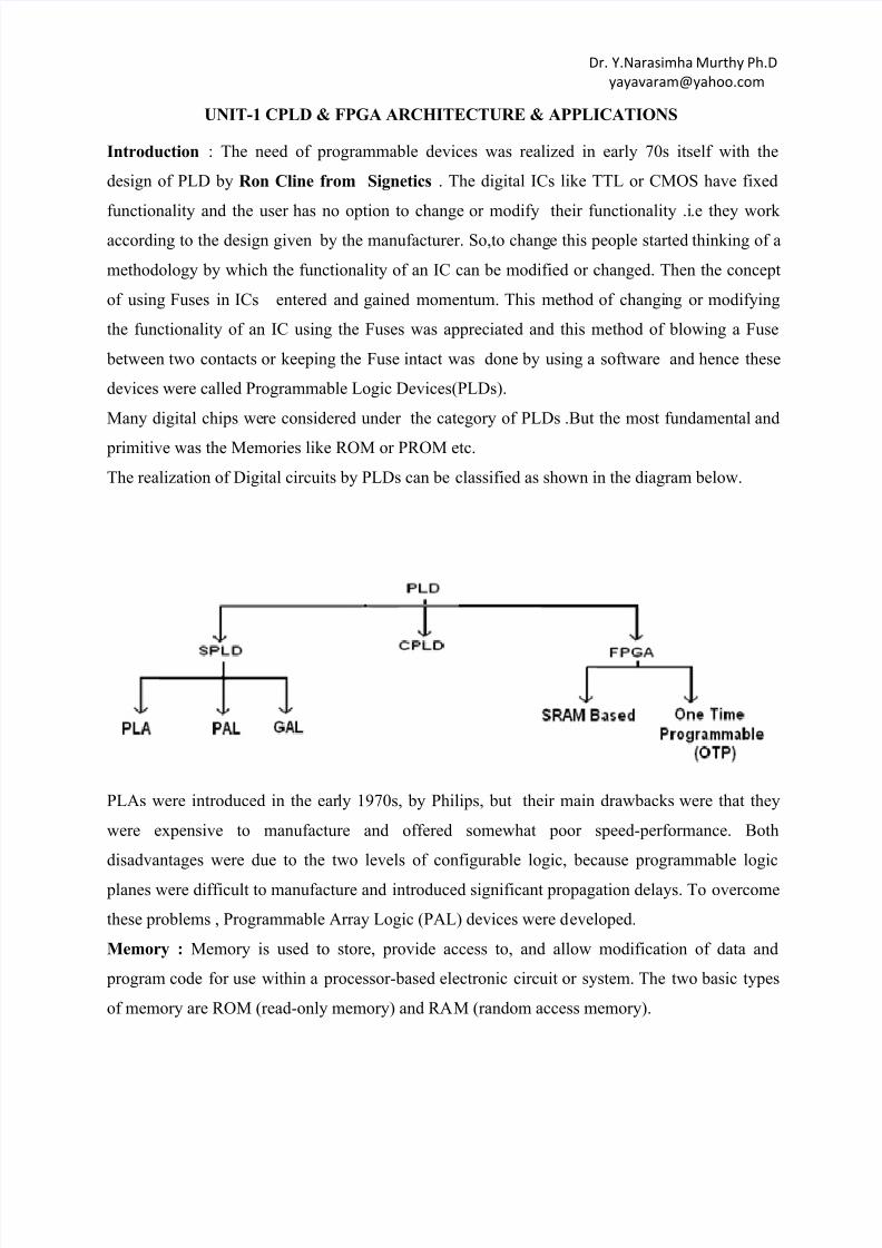
The realization of Digital circuits by PLDs can be classified as shown in the diagram below.
PLAs were introduced in the early 1970s, by Philips, but their main drawbacks were that they
were expensive to manufacture and offered somewhat poor speed-performance. Both
disadvantages were due to the two levels of configurable logic, because programmable logic
planes were difficult to manufacture and introduced significant propagation delays. To overcome
these problems , Programmable Array Logic (PAL) devices were developed.
Memory : Memory is used to store, provide access to, and allow modification of data and
program code for use within a processor-based electronic circuit or system. The two basic types
of memory are ROM (read-only memory) and RAM (random access memory).

8/13/2019 UNIT-I : CPLD & FPGA ARCHITECTURES & APPLICATIONS
http://slidepdf.com/reader/full/unit-i-cpld-fpga-architectures-applications 2/22
Dr. Y.Narasimha Murthy Ph.D
ROM is used for holding program code that must be retained when the memory power is
removed. It is considered to provide nonvolatile storage. The code can either be fixed when the
memory is fabricated (mask programmable ROM) or electrically programmed once (PROM,
Programmable ROM) or multiple times. Multiple programming capacity requires the ability to
erase prior programming, which is available with EPROM (electrically programmable ROM,
erased using ultraviolet [UV] light), EEPROM or EEPROM (electrically erasable PROM), or
flash (also electrically erased). PROM is sometimes considered to be in the same category of
circuit as programmable logic, although in this text, PROM is considered in the memory
category only.
RAM is used for holding data and program code that require fast access and the ability to modify
the contents during normal operation. RAM differs from read-only memory (ROM) in that it can
be both read from and written to in the normal circuit application. However, flash memory can
also be referred to as nonvolatile RAM (NVRAM). RAM is considered to provide a volatile
storage, because unlike ROM, the contents of RAM will be lost when the power is removed.
There are two main types of RAM: static RAM (SRAM) and dynamic RAM (DRAM).
ROM- READ ONLY MEMORY : A ROM is essentially a memory device for storage purpose
in which a fixed set of binary information is stored. The user must first specify the binary
information to be stored and then it is embedded in the unit to form the required interconnection
pattern. ROM contains special internal links that can be fused or broken. Certain links are to be
broken or blown out to realize the desired interconnections for a particular application and to
form the required circuit path. Once a pattern is established for a ROM, it remained fixed even if
the power supply to the circuit is switched off and then switched on again.
The block diagram of ROM is shown below. It consists of n input lines and m-output lines.
Each bit combination of input variables is called an address and each bit combination that is
formed at output lines is called a word. Thus, an address is essentially binary number that
denotes one of the min-terms of n variables and the number of bits per word is equal to the
number of output lines m. It is possible to generate p = 2n number of distinct addresses from n
number of input variables. Since there are 2n distinct addresses in a ROM, there are 2
n distinct
words which are said to be stored in the device and an output word can be selected by a unique
address. The address value applied to the input lines specifies the word at output lines at any

8/13/2019 UNIT-I : CPLD & FPGA ARCHITECTURES & APPLICATIONS
http://slidepdf.com/reader/full/unit-i-cpld-fpga-architectures-applications 3/22
Dr. Y.Narasimha Murthy Ph.D
given time. A ROM is characterized by the number of words 2n and number of bits per word m
and denoted as 2n × m ROM.
For example a 32 × 8 ROM contains 32 words of 8 bits each. This means there are eight output
lines and there are 32 numbers of distinct words stored in that unit, each of which is applied to
the output lines. The particular word selected from the presently available output lines is
determined by five input variables, as there are five input lines for a 32 × 8 ROM, because 25 =
32. Five input variables can specify 32 addresses or min-terms and for each address input there is
a unique selected word. Thus, if the input address is 0000, word number 0 is selected. For
address 0001, word number 1 is selected and so on.
A ROM is sometimes specified by the total number of bits it contains, which is 2n
× m. For
example, a 4,096-bit ROM may be organized as 512 words of 8 bits each. That means the device
has 9 input lines (29
× m = 512) and 8 output lines.
In Figure below, the block consisting of an AND array with buffers or inverters is equivalent to a
decoder. The decoder basically is a combinational circuit that generates 2n numbers of minterms
from n number of input lines. 2n or p numbers of minterms are realized from n number of input
variables with the help of n numbers of buffers, n numbers of inverters, and 2n numbers of AND
gates.

8/13/2019 UNIT-I : CPLD & FPGA ARCHITECTURES & APPLICATIONS
http://slidepdf.com/reader/full/unit-i-cpld-fpga-architectures-applications 4/22
Dr. Y.Narasimha Murthy Ph.D
Each of the minterms is applied to the inputs of m number of OR gates through fusible links.
Thus, m numbers of output functions can be produced after blowing of some selected fuses. The
equivalent logic diagram of a 2n×m ROM is shown below
ROM has many important applications in the design of digital computer systems. Realization of
complex combinational circuits, code conversions, generating bit patterns, performing arithmetic
functions like multipliers, forming look-up tables for arithmetic functions, and bit patterns forcharacters are some of its applications. They are particularly useful for the realization of multiple
output combinational circuits with the same set of inputs. As such, they are used to store fixed bit
patterns that represent the sequence of control variables needed to enable the various operations
in the system. They are also used in association with microprocessors and microcontrollers.

8/13/2019 UNIT-I : CPLD & FPGA ARCHITECTURES & APPLICATIONS
http://slidepdf.com/reader/full/unit-i-cpld-fpga-architectures-applications 5/22
Dr. Y.Narasimha Murthy Ph.D
PROGRAMMABLE LOGIC DEVICE-(PLD): The logic devices other than TTL ,CMOS
families whose logical operation is specified by the user through a process called programming
are called Programmable Logic Devices. So, the programmable logic device is the IC that
contain digital logic cells and programmable interconnect . The idea of PLD was first conceived
by Ron Cline from Signetics in 1975 with programmable AND and OR planes. The basic idea
with these devices is to enable the designer to configure the logic cells and interconnect to form a
digital electronic circuit within a single IC package. Here, the hardware resources will be
configured to implement a required functionality. By changing the hardware configuration, the
PLD will operate a different function. The functioning and basic working principle of PLD is
explained below through the diagrams.

8/13/2019 UNIT-I : CPLD & FPGA ARCHITECTURES & APPLICATIONS
http://slidepdf.com/reader/full/unit-i-cpld-fpga-architectures-applications 6/22
Dr. Y.Narasimha Murthy Ph.D
There are three types of PLD available. The simple programmable logic device (SPLD), the
Complex programmable logic device(CPLD), and the Field programmable gate array (FPGA).
Device Type AND Array OR Array
ROM Fixed Programmable
PLA Programmable Programmable
PAL Programmable Fixed
Simple Programmable Logic Device (SPLD)
The PLD with simple architectural features can be called as SPLD or Simple programmable
Logic Device. The SPLD was introduced prior to the CPLD and FPGA. Based on the
architecture the SPLDs are classified into three types. Programmable logic array (PLA),
Programmable array of logic (PAL), and Generic Array of Logic (GAL).
PLA-Programmable Logic Array
PLA, Programmable Logic Array is a type of LSI device and conceptually similar to a ROM.
However, a PLA does not contain all AND gates to form the decoder or does not generate all the

8/13/2019 UNIT-I : CPLD & FPGA ARCHITECTURES & APPLICATIONS
http://slidepdf.com/reader/full/unit-i-cpld-fpga-architectures-applications 7/22
Dr. Y.Narasimha Murthy Ph.D
minterms like ROM. In the PLA, the decoder is replaced by a group of AND gates with
buffers/inverters, each of which can be programmed to generate some product terms of input
variable combinations that are essential to realize the output functions. The AND and OR gates
inside the PLA are initially fabricated with the fusible links among them. The required Boolean
functions are implemented in sum of the products form by opening the appropriate links and
retaining the desired connections.
So, the PLA consists of two programmable planes AND and OR planes . The AND plane
consists of programmable interconnect along with AND gates. The OR plane consists of
programmable interconnect along with OR gates. In this view, there are four inputs to the PLA
and four outputs from the PLA. Each of the inputs can be connected to an AND gate with any of
the other inputs by connecting the crossover point of the vertical and horizontal interconnect
lines in the AND gate programmable interconnect. Initially, the crossover points are not
electrically connected, but configuring the PLA will connect particular cross over points
together. In this view, the AND gate is seen with a single line to the input. This view is by
convention, but this also means that any of the inputs (vertical lines) can be connected. Hence,
for four PLA inputs, the AND gate also has four inputs. The single output from each of the AND
gates is applied to an OR gate programmable inter connect.

8/13/2019 UNIT-I : CPLD & FPGA ARCHITECTURES & APPLICATIONS
http://slidepdf.com/reader/full/unit-i-cpld-fpga-architectures-applications 8/22
Dr. Y.Narasimha Murthy Ph.D
Again, the crossover points are initially not electrically connected, but configuring the PLA will
connect particular crossover points together. In this view, the OR gate is seen with a single line
to the input. This view is by convention, but this also means that any of AND gate outputs can be
connected to the OR gate inputs. Hence, for four AND gates, the OR gate also has four inputs
Therefore, the function is implemented in either AND-OR form when the output link across
INVERTER is in place, or in AND-OR-INVERT form when the link is blown off. The general
structure of a PLA with internal connections is shown in figure below.

8/13/2019 UNIT-I : CPLD & FPGA ARCHITECTURES & APPLICATIONS
http://slidepdf.com/reader/full/unit-i-cpld-fpga-architectures-applications 9/22
Dr. Y.Narasimha Murthy Ph.D
The size of a PLA is specified by the number of inputs, the number of product terms,and the
number of outputs. The number of sum terms is equal to the number of outputs. The PLA
described in figure above is specified as n × p × m PLA. The number of programmable links is
2n × p + p × m + m, whereas that of ROM is 2n × m. A typical PLA of 16 × 48 × 8 has 16 input
variables, 48 product terms, and 8 output lines.
To implement the same combinational circuit, a 216 × 8 ROM is needed, which consists of 216
=
65536 minterms or product terms. So there is a drastic reduction in number of AND gates within
the PAL chip, thus reducing the fabrication time and cost.
PROGRAMMABLE ARRAY LOGIC (PAL) :
The first programmable device was the programmable array logic (PAL) developed by
Monolithic Memories Inc(MMI). The Programmable Array Logic or PAL is similar to PLA,
but in a PAL device only AND gates are programmable. The OR array is fixed by the
manufacturer. This makes PAL devices easier to program and less expensive than PLA. On the
other hand, since the OR array is fixed, it is less flexible than a PLA device.

8/13/2019 UNIT-I : CPLD & FPGA ARCHITECTURES & APPLICATIONS
http://slidepdf.com/reader/full/unit-i-cpld-fpga-architectures-applications 10/22
Dr. Y.Narasimha Murthy Ph.D
The PAL device. has n input lines which are fed to buffers/inverters. Buffers/inverters are
connected to inputs of AND gates through programmable links. Outputs of AND gates are then
fed to the OR array with fixed connections. It should be noted that, all the outputs of an AND
array are not connected to an OR array. In contrast to that, only some of the AND outputs are
connected to an OR array which is at the manufacturer's discretion. This can be clarified by
above, which illustrates the internal connection of a four-input, eight AND-gates and three-
output PAL device before programming.
GAL-Generic Array Logic

8/13/2019 UNIT-I : CPLD & FPGA ARCHITECTURES & APPLICATIONS
http://slidepdf.com/reader/full/unit-i-cpld-fpga-architectures-applications 11/22
Dr. Y.Narasimha Murthy Ph.D
PAL and PLA devices are one-time programmable (OTP) based on PROM, so the PAL or PLA
configuration cannot be changed after it has been configured. This limitation means that the
configured device would have to be discarded and a new device configured. The GAL, although
similar to the PAL architecture, uses EEPROM and can be reconfigured.
The Generic Array Logic (GAL) device was invented by Lattice Semiconductor. The GAL was
an improvement on the PAL because one device was able to take the place of many PAL devices
or could even have functionality not covered by the original range. Its primary benefit, however,
was that it was erasable and re-programmable making prototyping and design changes easier for
engineers. The GAL is very useful in the prototyping stage of a design, when any bugs in the
logic can be corrected by reprogramming.
Complex Programmable Logic Device (CPLD):
CPLDs were pioneered by Altera, first in their family of chips called Classic EPLDs, and then
in three additional series, called MAX 5000, MAX 7000 and MAX 9000. The CPLD is the
complex programmable Logic Device which is more complex than the SPLD. This is build on
SPLD architecture and creates a much larger design. Consequently, the SPLD can be used to
integrate the functions of a number of discrete digital ICs into a single device and the CPLD can
be used to integrate the functions of a number of SPLDs into a single device.
So, the CPLD architecture is based on a small number of logic blocks and a global
programmable interconnect. Instead of relying on a programming unit to configure chip , it is
advantageous to be able to perform the programming while the chip is still attached to its circuit
board. This method of programming is known is called In-System programming (ISP). It is not
usually provided for PLAs (or) PALs , but it is available for the more sophisticated chips known
as Complex programmable logic device.

8/13/2019 UNIT-I : CPLD & FPGA ARCHITECTURES & APPLICATIONS
http://slidepdf.com/reader/full/unit-i-cpld-fpga-architectures-applications 12/22
Dr. Y.Narasimha Murthy Ph.D
The CPLD consists of a number of logic blocks or functional blocks, each of which contains a
macrocell and either a PLA or PAL circuit arrangement. In this view, eight logic blocks are
shown. The building block of the CPLD is the macro-cell, which contains logic implementing
disjunctive normal form expressions and more specialized logic operations. The macro cell
provides additional circuitry to accommodate registered or nonregistered outputs, along with
signal polarity control. Polarity control provides an output that is a true signal or a complement
of the true signal. The actual number of logic blocks within a CPLD varies; the more logic
blocks available, the larger the design that can be configured.
In the center of the design is a global programmable interconnect. This interconnect allows
connections to the logic block macrocells and the I/O cell arrays (the digital I/O cells of the
CPLD connecting to the pins of the CPLD package).The programmable interconnect is usually
based on either array-based interconnect or multiplexer-based interconnect. Array-based
interconnect allows any signal within the programmable interconnect to connect to any logic
block within the CPLD.

8/13/2019 UNIT-I : CPLD & FPGA ARCHITECTURES & APPLICATIONS
http://slidepdf.com/reader/full/unit-i-cpld-fpga-architectures-applications 13/22
Dr. Y.Narasimha Murthy Ph.D
This is achieved by allowing horizontal and vertical routing within the programmable
interconnect and allowing the crossover points to be connected or unconnected (the same idea as
with the PLA and PAL), depending on the CPLD configuration.
• Multiplexer-based interconnect uses digital multiplexers connected to each of the macrocell
inputs within the logic blocks. Specific signals within the programmable interconnect are
connected to specific inputs of the multiplexers. It would not be practical to connect all internal
signals within the programmable interconnect to the inputs of all multiplexers due to size
and speed of operation considerations.

8/13/2019 UNIT-I : CPLD & FPGA ARCHITECTURES & APPLICATIONS
http://slidepdf.com/reader/full/unit-i-cpld-fpga-architectures-applications 14/22
Dr. Y.Narasimha Murthy Ph.D
FPGAs – FIELD PROGRAMMABLE GATE ARRAYS
The FPGA concept emerged in 1985 with the XC2064TM FPGA family from Xilinx . The
“FPGA is an integrated circuit that contains many (64 to over 10,000) identical logic cells that
can be viewed as standard components.” The individual cells are interconnected by a matrix of
wires and programmable switches. A user's design is implemented by specifying the simple
logic function for each cell and selectively closing the switches in the interconnect matrix. The
array of logic cells and interconnect form a fabric of basic building blocks for logic circuits.
Complex designs are created by combining these basic blocks to create the desired circuit.
Unlike CPLDs (Complex Programmable Logic Devices) FPGAs contain neither AND nor OR
planes.The FPGA architecture consists of configurable logic blocks, configurable I/O blocks,
and programmable interconnect. Also, there will be clock circuitry for driving the clock signals
to each logic block, and additional logic resources such as ALUs, memory, and decoders may be
available. The two basic types of programmable elements for an FPGA are Static RAM and anti-
fuses.
Each logic block in an FPGA has a small number of inputs and one output. A look
up table (LUT) is the most commonly used type of logic block used within FPGAs.
There are two types of FPGAs.(i) SRAM based FPGAs and (ii) Antifuse technology based(OTP)
Every FPGA consists of the following elements
Configurable logic blocks(CLBs)
Configurable input output blocks(IOBs)
Two layer metal network of vertical and horizontal lines for interconnecting the CLBS
Configurable logic blocks(CLBs):
The configurable logic block is the basic logic cell and it is either RAM based or PLD based .
It consists of registers (memory), Muxes and combinatorial functional unit. An array of CLBS
are embedded within a set of vertical and horizontal channels that contain routing which can be personalized to interconnect CLBs.

8/13/2019 UNIT-I : CPLD & FPGA ARCHITECTURES & APPLICATIONS
http://slidepdf.com/reader/full/unit-i-cpld-fpga-architectures-applications 15/22
Dr. Y.Narasimha Murthy Ph.D
Configurable Input / Output logic locks (IOBs):
CLBs and routing channels are surrounded by a set of programmable I/Os which is
an arrangement of transistors for configurable I/O drivers.
Programmable interconnects:
These are un programmed interconnection resources on the chip which have
channeled routing with fuse links. Four types of interconnect architectures are available. They
are
Row-Column Architecture
Island Style Architecture
Sea-of-Gates Architecture
Advantages of FPGAs:
Design cycle is significantly reduced. A user can program an FPGA design in a few
minutes or seconds rather than weeks or months required for mask programmed parts.
High gate density i.e, it offers large gate counts.

8/13/2019 UNIT-I : CPLD & FPGA ARCHITECTURES & APPLICATIONS
http://slidepdf.com/reader/full/unit-i-cpld-fpga-architectures-applications 16/22
Dr. Y.Narasimha Murthy Ph.D
No custom masks tooling is required (Low cost).
Low risk and highly flexible.
Reprogram ability for some FPGAs (design can be altered easily).
Suitable for prototyping.
Parallelism
Allows for system-level extraction of parallelism to match input data
at design time
Huge computational capability
Fast development and Dynamic reconfiguration
Updating new pattern matching rules (or simply rules)
Device should not stop when updating new rules
Update time for new rules
To provide fast response to new attacks, the compilation and updating
time for new rules needs to be short
In case of a hardwired FPGA architecture, the update time is mostly dependent
on place & route time
Memory-based units can provide near instantaneous updates
Limitations:
Speed is comparatively less.
The circuit delay depends on the performance of the design implementation tools.
The mapping of the logic design into FPGA architecture requires sophisticated design
implementation (CAD) tools than PLDs.
FPGA Programming Technologies:
(a) Antifuse Technology:
An antifuse is a two terminal device that when un-programmed has a very high resistance
between the two terminals and when programmed, or “blown”, creates a very low resistance or
permanent connection. The application of a high voltage from 11 V to 21 V will create the low
resistive permanent connection. Antifuse technologies come in two types. The first is oxide-
nitride-oxide (ONO) dielectric based and the other is amorphous silicon or metal-to-metal
antifuse structures.

8/13/2019 UNIT-I : CPLD & FPGA ARCHITECTURES & APPLICATIONS
http://slidepdf.com/reader/full/unit-i-cpld-fpga-architectures-applications 17/22
Dr. Y.Narasimha Murthy Ph.D
Dielectric based antifuses consist of a dielectric material between N+ diffusion and polysilicon
which breaks down when a high voltage is applied. Early dielectrics were a single-layered oxide
dielectric until Actel came out with the programmable low impedance circuit element (PLICE),
which is a multi-layer oxide-nitride-oxide (ONO) dielectric fuse. A high voltage across the
PLICE melts the dielectric and creates polycrystalline silicon between the terminals. When the
PLICE is blown, it adds three layers rather than the double metal CMOS process. The layers are
a thin layer of oxide an top off the N+ surface, Low-pressure Chemical Vapor Deposition
(LPCVD) nitride and the reoxidized top oxide. The programming current has an important effect
because the higher the current during programming, the lower the link resistance, resulting in
smaller thickness for the antifuse material. Programming circuits for antifuses need to supply
high currents (15 ma for Actel) to insure high reliability and performance.
Amorphous silicon antifuse technology is the alternative to dielectric antifuse. It consists of
amorphous silicon between two layers of metal that changes phases when current is applied.
When the antifuse is not programmed the amorphous silicon has a resistance of 1 Giga ohm.
When a high current (about 20 mA) is applied to the anitfuse the amorphous silicon changes into
a conductive polysilicon link. Quick Logic pASIC FPGA is a perfect example of an amorphous
silicon antifuse technology.
(b). SRAM-based Technology:
SRAM FPGA architecture consists of static RAM cells to control pass gates or multiplexers.
The FPGA speed is determined by the delay introduced by the logic cells and the routing
channels. Multiplexers, look-up tables and output drivers affect the speed of signals through the
logic cells. An FPGA with more PIPs is easier to route but introducing more routing delay. The
size of the look-up table plays an important role depending on the design. Smaller LUTs provide
higher density but larger ones are preferred for high-speed applications.
Distinguish between SRAM and Antifuse Technologies: The following points explains the
differences between the two technologies.
1. Antifuse programming technology is faster than SRAM programming technology due to the
RC delays introduced by the interconnect structure.
2. Antifuse technology has more silicon area per gate and is easier to route than SRAM
technology.

8/13/2019 UNIT-I : CPLD & FPGA ARCHITECTURES & APPLICATIONS
http://slidepdf.com/reader/full/unit-i-cpld-fpga-architectures-applications 18/22
Dr. Y.Narasimha Murthy Ph.D
3. A disadvantage of antifuse FPGA is that they require more process layers and mask steps and
also contain high voltage programming transistors.
4. SRAM-based technology contains higher capacity than antifuse technologies.
5. SRAM based technology is very flexible with in-system programmability and the ability to
reconfigure the design during the debugging stage while antifuse technology is one-time
programmable (OTP). This ability reduces design and development, which reduces overall
cost of the design. Another advantage to this is that SRAM technology can be programmed at
the factory through complete verification test where the antifuse are tested as “blanks” and
require programming by the user to verify design requirements and operation.
6. A disadvantage of SRAM technology is that it is volatile meaning it has to be reprogrammed
every time power is turned off and on again. The SRAM usually require an extra memory
element to program the chip which occupies board space .
Altera’s FLEX 10K Series CPLDs
Altera‟s FLEX 10K devices are the industry‟s first embedded PLDs. Based on reconfigurable
CMOS SRAM elements, the Flexible Logic Element MatriX (FLEX) architecture incorporates
all features necessary to implement common gate array mega functions. With 10,000 to 250,000
typical gates ,the FLEX 10K family provides the density, speed, and features to integrate entire
systems, including multiple 32-bit buses, into a single device.
FLEX 10K devices are reconfigurable .So, the designer is not required to generate test vectorsfor fault coverage purposes. Additionally, the designer need not manage inventories of different
ASIC designs; FLEX 10K devices can be configured on the board for the specific functionality
required.
Each FLEX 10K device contains an Embedded Array (EA) and a Logic Array (LA).
The Embedded Array is used to implement a variety of memory functions or complex logic
functions, such as digital signal processing (DSP) ,microcontroller, wide-data-path manipulation,
and data-transformation functions.

8/13/2019 UNIT-I : CPLD & FPGA ARCHITECTURES & APPLICATIONS
http://slidepdf.com/reader/full/unit-i-cpld-fpga-architectures-applications 19/22
Dr. Y.Narasimha Murthy Ph.D
The Logic Array performs the same function as the sea-of-gates in the gate array: it is used to
implement general logic, such as counters, adders, state machines, and multiplexers.
The combination of embedded and logic arrays provides the high performance and high density
of embedded gate arrays, enabling designers to implement an entire system on a single device.
FLEX 10K devices are configured at system power-up with data stored in an Altera serial
configuration device or provided by a system controller.
Logic Element is , the smallest unit of logic in the FLEX 10K architecture, has a compact size
that provides efficient logic utilization. Each LE contains a four-input LUT, which is a function
generator that can quickly compute any function of four variables. In addition, each LE contains
a programmable flip flop with a synchronous enable, a carry chain, and a cascade chain. Each LE
drives both the local and the Fast Track. The programmable flip flop in the LE can be configured
for D, T, JK, or SR operation. The clock, clear, and preset control signals on the flip flop can be
driven by global signals, general-purpose I/O pins, or any internal logic. For combinatorial
functions, the flip flop is bypassed and the output of the LUT drives the output of the LE.

8/13/2019 UNIT-I : CPLD & FPGA ARCHITECTURES & APPLICATIONS
http://slidepdf.com/reader/full/unit-i-cpld-fpga-architectures-applications 20/22
Dr. Y.Narasimha Murthy Ph.D
The carry chain provides a very fast (as low as 0.2 ns) carry-forward function between Les. The
carry-in signal from a lower-order bit drives forward into the higher-order bit via the carry chain,
and feeds into both the LUT and the next portion of the carry chain. This feature allows the
FLEX 10K architecture to implement high-speed counters, adders, and comparators of arbitrary
width efficiently.
Cascade Chain in the FLEX 10K architecture can implement functions that have a very wide
fan-in. Adjacent LUTs can be used to compute portions of the function in parallel; the cascade
chain serially connects the intermediate values. The cascade chain can use a logical AND
or logical OR (via De Morgan‟s inversion) to connect the outputs of adjacent Les. Each
additional LE provides four more inputs to the effective width of a function, with a delay as low
as 0.7 ns per LE. Cascade chain logic can be created automatically by the Compiler during
design processing, or manually by the designer during design entry.
Altera offers the EPC1, EPC2, EPC16, and EPC1441 configuration devices, which configure
FLEX 10K devices via a serial data stream. Configuration data can also be downloaded from
system RAM or from Altera‟s Bit Blaster serial download cable or Byte Blaster MV parallel port
download cable.
Even after configuring a FLEX 10K device , it can be reconfigured in-circuit by resetting the
device and loading new data .Because reconfiguration requires less than 320 ms, real-time
changes can be made during system operation. FLEX 10K devices contain an optimized interface
that permits microprocessors to configure FLEX 10K devices serially or in parallel, and
synchronously or asynchronously. The interface also enables microprocessors to treat a FLEX
10K device as memory and configure the device by writing to a virtual memory location, making
it very easy for the designer to reconfigure the device.
SPEED PERFORMANCE :
The speed performance of PLDs is affected by their architectural features like I/O blocks, Logic
Elements and the Interconnects. The routing of these elements also paly an important role.For example
if a finite state machine is to be implemented in an FPGA, then the amount of logic feeding each
state machine flip-flop must be minimized. This follows because in FPGAs flip-flops are directly
fed by logic blocks that have relatively few inputs (typically 4 - 8). If the state machine flip-flops
are fed by more logic than will fit into a single logic block, then multiple levels of logic blocks

8/13/2019 UNIT-I : CPLD & FPGA ARCHITECTURES & APPLICATIONS
http://slidepdf.com/reader/full/unit-i-cpld-fpga-architectures-applications 21/22
Dr. Y.Narasimha Murthy Ph.D
will be needed, and speed-performance will decrease. Even in a CPLD architecture, speed-
performance of a state machine can be significantly affected by state bit encoding,for example, in
the Altera MAX 7000 CPLDs, flip-flops that are fed by five or fewer product terms will operate faster
than those that require more than five terms.
CPLDS are ideal for high-speed applications requiring critical timing and FPGAs are more
flexible with the finer-grained architecture. Lattice semiconductor CPLD series architecture
offered predictable timing, high densities, in-system programmability, flexible architecture for
mixed combinatorial and register intensive designs and system partitioning. Some applications
can not use CPLDs. Planetary Spacecraft and earth orbiting satellites and science instruments
require Radiation Hardened PLDs. Between CPLD and FPGAs ,the CPLDs are fast and ,
predictable but the FPGAs are application dependent.
The CPLD implementation of the sequential circuit is much faster than the FPGA version.
However, the most interesting aspect is the difference between the 5 -bit and13-bit versions of
the circuit. If both versions are operated at 100 MHz for CPLD implementation, while the 13-
bit version is much slower than its smaller counterpart for the FPGA. This is a good example of
how FPGAs are not suitable for implementing circuits that require “wide” logic gates (the 14 -
inputAND-gates for this example), whereas CPLDs can easily implement such applications.
It is widely accepted by designers who use PLDs that FPGAs are the best choice for data-path
circuits, because wide logic gates are not required and the number of flip-flops needed is large.
But it is true that the FPGAs cannot provide required performance in an FPGA, and the CPLDs
were successful . The reason that the CPLDs provided better performance is to do with their
simple structure that provides for very high-speed paths from input pins, through AND-OR logic
and flip-flops, to output pins.
It is also found experimentally that the CPLD-based counters achieve the maximum possible
speed of t pd plus the setup time of the flip-flop. This is because each counter bit needs up to 34-
input AND functions that feed 4-input OR-gates .In the FLEX devices, high-speed carry chain is
employed to implement the required wide AND. It is the speed of this carry chain that limits the
speed-performance of the FLEX-based counter. Roughly, a counter of double the size has twice
the carry chain length and thus half the speed performance. So , the conclusion is Altera CPLDs

8/13/2019 UNIT-I : CPLD & FPGA ARCHITECTURES & APPLICATIONS
http://slidepdf.com/reader/full/unit-i-cpld-fpga-architectures-applications 22/22
Dr. Y.Narasimha Murthy Ph.D
can implement very fast counters, however, it is difficult to construct many large counters in one device.
The FLEX FPGAs are better suited for this purpose, but performance and routability are compromised
when the carry chain hardware is used. Both performance and routability can be improved by enhancing
the counter design with a very a small cost in area. However, these gains cannot be realized without
intimate knowledge of the FPGA architecture.
Ref erences :
1. „Architecture of Field-Programmable Gate Arrays‟ Jonathan Rose, Abbas EL Gamal, and
Alberto Sangiovanni-Vincentelli
2. Architecture of FPGAs and CPLDs: A Tutorial, Stephen Brown and Jonathan Rose
3.‟Designing for High Speed-Performance in CPLDs and FPGAs‟, Zeljko Zilic, Guy Lemieux
4.‟Digital Principles and Logic Design‟ A. SAHA N. MANNA