unit - 19 semiconductor electronics ug physics... · electronics 'rzqordghgiurpzzz...
TRANSCRIPT

321
Unit - 19Semiconductor
Electronics
Downloaded from www.studiestoday.com
Downloaded from www.studiestoday.com

322
SUMMARY
Conductor :- Presence of free electrons
Electrical resistivity is quite less
Insulator :- No free electrons
Very large electrical resistivity
Semi-conductor :-
Electrical resistance greater than conductor but smallar than insulator
At 0 K temperature it behaves like perfect insulator (in pure form)
Hole :- An empty space, when covalent bond breaks and electron gets escaped.
It is electron deficiency space called hole
behaves like positive electric charge.
For intrinsic (pure) semi-conductor :-
ni = n
e = n
h where n
i = Intrinsic electrical charge carrier density, n
e = number density of electrons
nh = number density of holes
Electrical conduction is due to both, electrons and holes
* Extrinsic semi-conductor :-
(1) N-type : Pentavalent impurity is added
Majority charge carrier are electrons
ne > n
h
(2) P-type : Trivalent imparity is added
Majority charge carries are holes
nh > n
e
* Valence Band :- Completely filled (with 4N electrons) lower band is called valence band
* Forbidden Gap :- The region above valance band without any available energy levels is called forbidden gap
* Conduction Band :- The region above forbidden gap is called conduction band
* Band Gap (Eg) :- The difference between minimum energy (Ec) of conduction band and maximum energy(Ev) of valence band is known as band gap energy
For Insulator Eg > 3eV
For Conductor Eg = 0
For semiconductor Eg < 3eV
Downloaded from www.studiestoday.com
Downloaded from www.studiestoday.com

323
* Depletion Region :-
A region near the junction which is deplete of respective majority charge carriers.
Thickness is about 0.5m
* Depletion Barrier :- The varying electrical potential near junction is called depletion barrier (0.7V for Siand 0.3V for Ge)
* Forward Bias :-
When P end of PN junction is connected to positive pole of the battery and N end is connectedto negative pole of the battery, then such an arrangement is called forward bias.
Depletion barrier (P.d) and Depletion region (width) is decreased.
* Reverse Bias :-
When P end of PN junction is connected to negative pole of the battery and N end is connectedto positive pole of the battery, then such an arrangement is called forward bias.
Depletion barrier (P.d) and depletion region (width) are increased
* Brekdown voltage :- In reverse bias condition of PN junction, for certain voltage, current increases suddenly.This certain voltage is called breakdown voltage.
* Zener effect :- Due to smaller width of depletion region even at small reverse bias voltage, electric fieldbecomes strong enough to break covalent bond, giving large number of electron hole pair is calledzener effect
* Avalanche effect :- Due to large width of depletion region, at only high reverse bias voltage electric field inthe depletion region becomes strong enough to break many covalent bonds, giving rise to so manycharge carrier is called avalanch effect and diode is called avalanche diode
* Regulated Power Supply :- If D.C. output voltage, in a rectifier circuit (or power supply) remains constantwith the charge in load current I
L, then such power supply is called reguluted power supply
* Rectification and Rectifier :- The process of obtaining D.C. voltage (or current) from A.C. voltage (orcurrent) is called rectification and circuit assembled for this process is called rectifier
* TRANSISTOR
Transistor is a device made of two PN junctions
Junction between base and emitter is called emitter junction
Junction between base and collector is called collector junction
For proper working of transistor, emitter junction should be forward biased and collectorjunction should be reverse biased
A.C. parameters for a transistor
(1) Input resistance = ri =
CE
BE
B V cons tan t
VI
Downloaded from www.studiestoday.com
Downloaded from www.studiestoday.com

324
(2) Output resistance = ro =
B
CE
C I cons tan t
VI
(3) A.C. current gain CE
i acB V cons tan t
IcAI
(4) Transconductance = gm
= C
BE i
I acV r
D.C. Parameters of a transistor
(1) IE = I
B + I
C
(2) Current gain for CB circuit Cdc
E
II
dc 1
(3) Current gain for CE cicuit = Cdc
B
II
dc 1
Voltage gain for CE Amplifier
CE acL m L
BE i
VAv R g RV r
Power gain for CE Amplifier
2 Lp v i ac
i
RA A Ar
* Oscillator :- Certain electronic circuits can generated any arbitrary frequency with desired amplitude of
voltage and current. Such circuit is known as oscillator.
Oscillator frequency 1f2 LC
* Logic gate :-
The logic circuit, with one or more than one input but only one output is called logic gate.
Basic logic gates are OR gate, AND gate and NOT gate
Universal logic gates are NAND gate and NOR gate
Downloaded from www.studiestoday.com
Downloaded from www.studiestoday.com
325
* LOGIC GATES
A digital circuit with one or more input signals but only one output signal is known as logical gate.
The logic gates are the building blocks of a digital system. Each logic gate follows a certain logicalrelationship between input and output voltage.
There are three basic logic gates :
OR gate
AND gate
NOT gate
Truth table
It is a table that shows all possible input combinations and corresponding output combination for a logicgate.
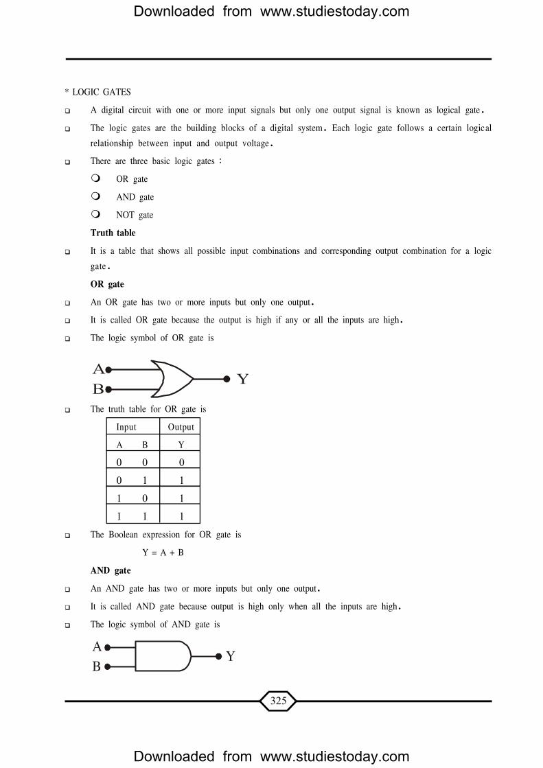
OR gate
An OR gate has two or more inputs but only one output.
It is called OR gate because the output is high if any or all the inputs are high.
The logic symbol of OR gate is
AB
Y
The truth table for OR gate is
Input Output
A B Y
0 0 00 1 11 0 11 1 1
The Boolean expression for OR gate is
Y = A + B
AND gate
An AND gate has two or more inputs but only one output.
It is called AND gate because output is high only when all the inputs are high.
The logic symbol of AND gate is
AB
Y
Downloaded from www.studiestoday.com
Downloaded from www.studiestoday.com

326
The truth table for AND gate is
Input Output
A B Y0 0 00 1 01 0 01 1 1
The Boolean expression for AND gate is Y = A.BNOT gate
The NOT gate is the simplest of all logic gates. It has only one input and one output. NOT gate is also called inverter because it inverts the input. The logic symbol of NOT gate is
A Y
The truth table for NOT gate isInput OutputA Y0 11 0
The Boolean expression for NOT gate is Y = ANAND gate
It is an AND gate followed by a NOT gate. The logic symbol for NAND gate is
AB
Y
The truth table for NAND gate isInput OutputA B Y0 0 10 1 11 0 11 1 0
The Boolean expression for NAND gate is
Y A B
Downloaded from www.studiestoday.com
Downloaded from www.studiestoday.com

327
NOR gate
It is an OR gate followed by a NOT gate.
The logic symbol of NOR gate is
AB
Y
The truth table for NOR gate is
Input Output
A B Y
0 0 1
0 1 0
1 0 0
1 1 0
The Boolean expression for NOR gate is
Y A B
Exclusive OR gate or XOR gate
The logic symbol of XOR gate is
AB
Y
The truth table for XOR gate is
Input Output
A B Y
0 0 0
0 1 1
1 0 1
1 1 0
The Boolean expression for XOR gate is
Y A B A B A B
Downloaded from www.studiestoday.com
Downloaded from www.studiestoday.com

328
Exlusive NOR gate or XNOR gate
The logic symbol of XNOR gate is
AB
Y
The truth table for XNOR gate isInput OutputA B Y0 0 10 1 01 0 01 1 1
The Boolean expression for XNOR gate is
Y A B A B A B
NAND as a universal gate NAND gate is called as universal gate because with the repeated use of NAND gate we can construct any
basic gate
NOT gate from NAND gate
A Y
Y A
AND gate from NAND gates
A A BYB
OR gate from NAND gates
A
B
A
B
Y
Y A B A B A B
Downloaded from www.studiestoday.com
Downloaded from www.studiestoday.com
329
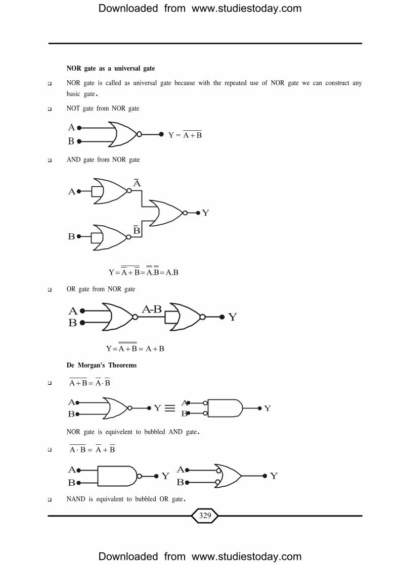
NOR gate as a universal gate
NOR gate is called as universal gate because with the repeated use of NOR gate we can construct anybasic gate.
NOT gate from NOR gate
AB
Y = A B
AND gate from NOR gate
A
B
A
B
Y
Y A B A.B A.B
OR gate from NOR gate
A A-BB Y
Y A B A B
De Morgan's Theorems
A B A B
AB Y
AB
Y
NOR gate is equivelent to bubbled AND gate.
A B A B
AB
YAB
Y
NAND is equivalent to bubbled OR gate.
Downloaded from www.studiestoday.com
Downloaded from www.studiestoday.com

330
Boolean identities
A + B = B + A A B = B A
A + (B + C) = (A + B) + C A (B C) = (A B) C
A (B + C) = A B + A C A + B C = (A + B) (A + C)
A + 0 = A A 1 = AA + 1 = 1 A 0 = 0A + A = A A A = A
A A 1 A A 0
A A A A
A B A.B A.B A B
A + A B = A A (A + B) = A
A A B A B A A B A B
MCQFor the answer of the following questions choose the correct alternative from
among the given ones.(1) C, Si and Ge have same no. of valence electrons. C is an insulator because energy required to take one
electron out from(A) Si is more (B) C is more (C) Ge is more (D) C is less
(2) Ionization energy of isolated phosphorous atonis 10 eV. Ionization energy of same atom in Si is nearly eV (Relative Permitivity of silicon = 12)
(A) 0.1 (B) 0.2 (C) 0.3 (D) 0.4(3) By adding impurity in intrinsic semiconductor P type semiconductor is made. charge of
these P type semiconductor is
(A) trivalent, neutral (B) pentaralent, neutral (C) pentavalent, positive (D) trivalent, negative
(4) Strong overlaping of different atomic orbitals makes
(A) different energy level (B) energy band (C) Conductor (D) Insulators(5) We can not make p-n junction diode by making P type semi-condutor join with N - type semi-conductor,
because
(A) Inter-atomic spacing becomes less than 1AO
(B) P - type will repel N - type
(C) There will be discontinuity for the flowing charge carriers
(D) semi-conducting properties will be lost
Downloaded from www.studiestoday.com
Downloaded from www.studiestoday.com

331
(6) For p-n junction, which statement is incorrect
(A) Donor atoms are depleted of their holes in junction
(B) No net charge exists far from junction
(C) Barrier potential VB is generated
(D) Energy VB is to be surmounted before any charge can flow across junction
(7) The intrinsic semi-conductor has :
(A) a finite resistance which does not change with temperature
(B) infinite resistance which decreases with temperature
(C) Finite resistance which decreases with temperature
(D) Finite resistance which does not change with temperature
(8) The behaviour of Ge as semi-conductor is due to width of :
(A) Conduction band being large
(B) Forbidden band being large
(C) Conduction band being small
(D) Forbidden band being small and narrow
(9) Which of the following is not the advantage of PN junction diode over tube valve ?
(A) Unlimited life (B) No warming-up time after switching
(C) Large efficiency (D) Low consumption of Power
(10) The forward biased diode is
(A) (B)
(C) (D)
(11) A gate has the following truth table :
The gate is :
(A) OR (B) NOR (C) NAND (D) AND
Downloaded from www.studiestoday.com
Downloaded from www.studiestoday.com
332
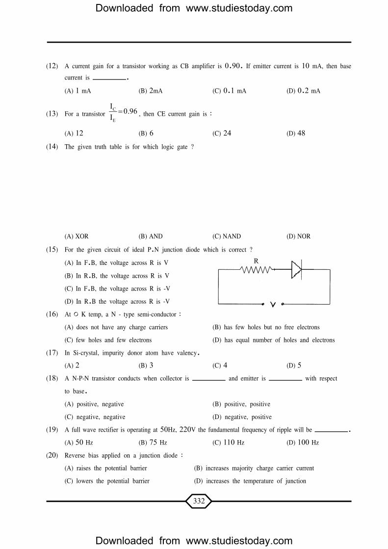
(12) A current gain for a transistor working as CB amplifier is 0.90. If emitter current is 10 mA, then basecurrent is .
(A) 1 mA (B) 2mA (C) 0.1 mA (D) 0.2 mA
(13) For a transistor C
E
I 0.96I , then CE current gain is :
(A) 12 (B) 6 (C) 24 (D) 48
(14) The given truth table is for which logic gate ?
(A) XOR (B) AND (C) NAND (D) NOR
(15) For the given circuit of ideal P.N junction diode which is correct ?
(A) In F.B, the voltage across R is V
(B) In R.B, the voltage across R is V
(C) In F.B, the voltage across R is -V
(D) In R.B the voltage across R is -V
(16) At 0 K temp, a N - type semi-conductor :
(A) does not have any charge carriers (B) has few holes but no free electrons
(C) few holes and few electrons (D) has equal number of holes and electrons
(17) In Si-crystal, impurity donor atom have valency.
(A) 2 (B) 3 (C) 4 (D) 5(18) A N-P-N transistor conducts when collector is and emitter is with respect
to base.
(A) positive, negative (B) positive, positive
(C) negative, negative (D) negative, positive
(19) A full wave rectifier is operating at 50Hz, 220V the fundamental frequency of ripple will be .
(A) 50 Hz (B) 75 Hz (C) 110 Hz (D) 100 Hz
(20) Reverse bias applied on a junction diode :
(A) raises the potential barrier (B) increases majority charge carrier current
(C) lowers the potential barrier (D) increases the temperature of junction
R
Downloaded from www.studiestoday.com
Downloaded from www.studiestoday.com

333
(21) In the figure, the input is across A and C and output is across B and D. The output is
(A) same as input
(B) Halfwave rectified
(C) Fullwave rectified
(D) zero
(22) In the figure, the input is across B and D and output is across A and C. The output is
(A) same as input
(B) Halfwave rectified
(C) Fullwave rectified
(D) zero
(23) Digital circuits can be made to be respective use of :
(A) AND gate (B) OR gate (C) NOT gate (D) NAND gate
(24) The output current versus time curve of a rectifier is shown in the figure. The avarage value of theoutput-current is .
(A) 0 (B) oI2
(C) O2I
(D) I0
(25) A sinusoidal voltage of peak value 200volts is connected to a diode and resistor R in the circuit shown.If diode is ideal, the r.m.s. voltage across R is volt.
(A) 100 (B) 200
2
(C) 200 (D) 280
(26) For a transistor, in a common base configuration the alternating current gain is given by :
(A) C
C
B V const.
II
(B) C
B
C V const.
II
(C) C
C
E V const.
II
(D) C
E
C V const.
II
(27) In a N-P-N transistor circuit, the emitter, collector and base current are respectively IE, I
C and I
B. The
relation between them is .
(A) IC < I
E < I
B(B) I
B < I
C < I
E(C) I
B > I
C < I
E(D) I
B > I
C > I
E
Output Current
Time
I0
Downloaded from www.studiestoday.com
Downloaded from www.studiestoday.com

334
(28) Assuming that the junction diode is ideal, the current through the diode is mA
(A) 1 (B) 10 (C) 20 (D) 30(29) The symbol respresents :
(A) NOT gate (B) OR gate (C) AND gate (D) NOR gate
(30) The combinations of NAND gates shown here under are equivqlent to :
(A) OR gate and NOT gate (B) AND gate and OR gate
(C) AND gate and NOT gate (D) OR gate and AND gate
(31) How many NAND gates are used to form AND gate ?
(A) 1 (B) 2 (C) 3 (D) 4(32) Ripples are .
(A) A.C. mixed with D.C (B) D.C. mixed with output
(C) D.C. output (D) A.C. output
(33) In an P.N.P transistor circuit, the collector current is 10 mA. If 90% of the electrons emitted reach thecollector :
(A) IE = 9mA (B) I
E = 10mA (C) I
B = 1mA (D) I
B = -1 mA
(34) When a P-type semi-conductor is heated :
(A) number of holes increases while that of electrons decreases
(B) number of electron increases while that of hole decreases
(C) number of electrons and holes remains same
(D) number of electrons and holes increases equally
(35) The depletion layer in PN junction diode is caused by
(A) drift of holes (B) Diffusion of impurity ions
(C) diffusion of charge carriers (D) drift of electrons
Downloaded from www.studiestoday.com
Downloaded from www.studiestoday.com

335
(36) The active junction area in a solar cell is as we want power
(A) small, more (B) small, small (C) large, more (D) large, small(37) The forbidden energy band gap in semi-conductor, conductor and insulator are E1, E2 and E3
respectively.The relation among then is :(A) E1 < E2 > E3 (B) E1 > E2 > E3 (C) E1 < E2 < E3 (D) E1 > E2 < E3
(38) An N-P-N Transistor circuit is shown in figure is(A) A common base circuit(B) A common emitter circuit(C) A common collector circuit(D) Oscillator circuit
(39) In a common emitter amplifier, output resistance is 5000 and input resistance is 1000 . If peakvalue of signal voltage is 1 mV and 100 , then the peak value of output voltage is
(A) 0.1V (B) 0.3V (C) 0.2V (D) 0.5V
(40) The A.C. current gain of a transistor is 100. If the base current changes by 100 A , What is thecharge in collector current ?
(A) 20 mA (B) 30 mA (C) 10 mA (D) 10 A(41) What is the output of the combination of the gates shown in the fig. below ?
(A) A A B (B) A + A B
(C) A B A B (D) A B A B
(42) The expression of Y in the following circuit is :(A) AB + CD(B) A + BCD(C) A + B + C + D(D) A B C D
(43) Which of the following figure represents an ideal diode characteristics ?
(A) (B)
(C) (D)
Downloaded from www.studiestoday.com
Downloaded from www.studiestoday.com

336
(44) In Ge sample, traces of gallium are added as impurity. The resultant sample would behave like :
(A) a conductor (B) a P-type semiconductor
(C) an N-type semiconductor (D) an insulator
(45) A light emitting diode has a voltage drop of 2V across it when 10mA current is passed. If this LED isto be operated with 6V battery the value of limiting resistor would be .
(A) 400 (B) 4000 (C) 40k (D) 300(46) NAND gate is .
(A) A basic gate (B) Not a universal gate
(C) A universal gate (D) Multipurpose gate
(47) The number of holes and electrons in an intrinsic conductors are x and y respectively at roomtemperature. Which of the following options are true ?
(A) x > y (B) y > x (C) x = y (D) x << y
(48) How will you increase the resistivity of Ge semi-conductor ?
(A) On adding donor impurity (B) On adding acceptor impurity
(C) On making UV light incident on Ge crystal (D) On decreasing the temperature
(49) What is type of material, for the energy band diagram shown in the figure ?
(A) N - type semi-conductor
(B) P - type semi-conductor
(C) Insulator
(D) Intrinsic semi-conductor
(50) From the following semi-conductor devices, operates in forward bias only.
(A) Varactar diode (B) Zener diode (C) Light emitting diode (D) photo-diode
(51) device is the odd-one out.
(A) solar-cell (B) Varactor diode (C) Photodiode (D) Zener diode
(52) The value of depletion capacitance on decreasing the reverse bias on varactor diode
(A) decreases (B) increases (C) becomes zero (D) does not change
(53) Which of the following statement is correct for transistor LC oscillator circuit ?
(A) It works with negative feed back
(B) The phase difference between output and input signal is radian
(C) To start oscillation external signal is required
(D) The frequency of output signal is independent of the components used in feed back circuit
Conduction Band
Valence Band
Downloaded from www.studiestoday.com
Downloaded from www.studiestoday.com

337
(54) The frequency of output signal of LC oscillator circuit is 100Hz with capacitance value 0.1 F . If value
of capacitance is taken as 0.2 F , the frequency of output signal .
(A) decreases by 12 (B) increases by
12 (C) decreases by
12 (D) increases by
12
(55) The Common Emmiter amplifier has voltage gain equal to 300 and its input signal is 0.5cos(100 t)
volt. The output signal will be equal to .
(A) 150 cos (100t) (B) 300 cos (100t)
(C) 150 cos (100t + ) (D) 300 cos (100t – )
(56) Common base current gain of a NPN transistor is 0.99. The input resistance is 1000 and load
resistance is 10,000 . The voltage gain in common emitter mode is .
(A) 9900 (B) 99000 (C) 99 (D) 990
(57) The logic circuit shown in the figure, is the equivalent diagram of which logic gate ?
(A) OR gate
(B) NAND gate
(C) AND gate
(D) NOR gate
(58) In forward bias made, the P.N junction diode resistance will .
(A) infinity (B) zero (C) less (D) more
(59) To obtain OR gate from NOR gate, you will need
(A) one NOR gate (B) one NOT gate (C) Two NOT gate (D) one OR gate
(60) For Boolean identities match the pair :
(1) A (P) A B
(2) A B (Q) A B
(3) A.B (R) A B
(4) A A B (S) A
(A) (1) - (S), (2) - (P), (3) - (Q), (4) - (R)
(B) (1) - (S), (2) - (R), (3) - (Q), (4) - (P)
(C) (1) - (S), (2) - (Q), (3) - (P), (4) - (R)
(D) (1) - (S), (2) - (R), (3) - (P), (4) - (Q)
Downloaded from www.studiestoday.com
Downloaded from www.studiestoday.com

338
(61) The ratio of concentration of electrons and holes in a semi-conductor is 75 and the ratio of currents is
74 , then what is the ratio of their drift velocities ?
(A) 47 (B)
58 (C)
45 (D)
54
(62) In a P-type silicon, which of the following statement is true ?
(A) Electrons are majority charge carries and trivalent atoms are the dopants
(B) Electrons are minority charge carries and pentavalent atoms are dopants
(C) Holes are minority charge carriess and pentavalent atoms are dopants
(D) Hole are majority charge carries and trivalent atoms are dopants
(63) In the circuit below A and B represnts two inputs and C represents output. The circuit
represents .
(A) NOR gate
(B) NAND gate
(C) AND gate
(D) OR gate
(64) A zener diode used as voltage regulator is connected .
(i) in forward bias (ii) in reverse bias (iii) in parallel with load (iv) in series with load
(A) (i) and (ii) are correct (B) (ii) and (iii) are correct
(C) only (i) is correct (D) only (iv) is correct
Directions : Question numbers (65), (66) and (67) are based on following passage.
PASSAGE : A n-p-n transistor is used in common emitter made in an amplifier circuit. A change of40 A in the base current changes the output current by 2mA and 0.04V in input voltage.
(65) The input resistance is .
(A) 1k (B) 10 (C) 10 k (D) 100
(66) The current amplification factor is .
(A) 20 (B) 30 (C) 50 (D) 40
(67) If a load of 6k is used, then the voltage gain of the amplifier is .
(A) 100 (B) 200 (C) 300 (D) 400
(68) An amplifier has voltage gain AV = 1000. The voltage gain in dB is .
(A) 20 dB (B) 30 dB (C) 3 dB (D) 60 dB
Downloaded from www.studiestoday.com
Downloaded from www.studiestoday.com

339
(69) A potential barrier of 0.6V exists across a P-N junction. If the depletion region is 1 m wide, what is the
intensity of electric field in the region ?
(A) 5 14 10 Vm (B) 5 15 10 Vm (C) 5 16 10 Vm (D) 5 12 10 Vm
(70) when a PN junction diode is forward biased, then the depletion region is and barrier heightis .
(A) reduced, increases (B) widened, reduced (C) reduced, reduced (D) increased, increased
(71) Which of the following circuit provides full wave rectification ?
(A) (B)
(C) (D)
(72) A common- emitter amplifier has a voltage gain of 100, an input impedence of 100 and an outputimpedence of 200 .The product of voltage gain and current gain is .
(A) 1000 (B) 3000 (C) 5000 (D) 500(73) A P-N photodiode is made of a material with a band gap of 2.0ev. The minimum frequency of the
radiation that can be absorbed by the material is nearly (Take hc = 1240eVnm)
(A) 145 10 Hz (B) 1420 10 Hz (C) 141 10 Hz (D) 1410 10 Hz
(74) The bodean equation for the circuit is
(A) Y A B C (B) Y A B C
(C) Y A B C (D) Y A B C
(75) A n-p-n transistor circuit has 0.985 . If Ic = 9 mA then the value of I
B is .
(A) 0.003mA (B) 0.66mA (C) 0.015mA (D) 0.03mA
(76) For a transistor amplifier, the voltage gain
(A) remains constant for all frequencies
(B) is high at high and low frequencies and constant in the mid-frequency range
(C) is low at high and low frequencies and constant in the mid-frequency range
(D) None of the above
Downloaded from www.studiestoday.com
Downloaded from www.studiestoday.com

340
(77) The current flowing through 10 resistor in the circuit shown in the figure is .
(A) 50mA (B) 20mA
(C) 40mA (D) 80mA
(78) The input and outputs from different time intervals are given below for NAND gate
Time interval Input A Input B Output Y
t1 to t2 0 1 P
t2 to t3 0 0 Q
t3 to t4 1 0 R
t4 to t5 1 1 S
The value taken by P, Q, R and S are respectively
(A) 1, 0, 1, 1 (B) 0, 1, 0, 0 (C) 0, 1, 0, 1 (D) 1, 1, 1, 0(79) The manifestation of band structure in solids is due to :
(A) Heisenberg's uncertainty principle
(B) Pauli's exclusion principle
(C) Bohr's correspondence principle
(D) Boltzmann's low
(80) Copper and silicon material is cooled down from 600K to 400K then, resistivity of cooper and silicon .
(A) increases, decreases (B) decreases, increases (C) decreases, decreases (D) increases, increases
(81) Semi-conductor has phospholous as impurity then it will have .
(A) ne>>n
h(B) n
e<<n
h(C) n
e = n
h(D) n
e = n
h = n
i
(82) Zener diode is used as
(A) Full. wave rectifier (B) amplifier
(C) A.C. voltage regulator (D) D.C. voltage regulator
(83) Break down voltage of a diode is 5V. By which effect this breakdown occurs in diode ?
(A) Only avalanche effect (B) Only zener effect
(C) Avalanche or zener effect (D) None of the above
(84) When NPN transistor is used as an amplifier then
(A) electron moves from base to collector
(B) hole travels from emitter to base
(C) hole goes to emitter from base
(D) electron goes to base from collector
Downloaded from www.studiestoday.com
Downloaded from www.studiestoday.com

341
(85) For a given amplifier circuit, to make transistor active as an amplifier, how much value of voltages to bekept for V
BB battery and V
CC battery ?
(A) VBB
= -1V VCC
= +5V
(B) VBB
= -1V VCC
= -5V
(C) VBB
= +1V VCC
= +5V
(D) VBB
= +1V VCC
= -5V
(86) Which of the following logic gate will have output 1 ?
(A) (B)
(C) (D)
(87) For gate, the output is 1 only when both input are `0'
(A) AND (B) NAND (C) OR (D) NOR
(88) In VLSI circuits more than gates are contained.
(A) 1000 (B) 100 (C) 10 (D) 500
(89) The flow of valence electrons to the left means that holes are flowing.
(A) Left (B) Right (C) Either way (D) None
(90) How many free electrons does a P-type semiconductor contain ?
(A) Many (B) None
(C) Only those produced by thermal energy (D) Same number as holes
(91) Suppose an intrinsic semi-conductor at room temperature has 1 billion free electrons at room temperature.If temperature changes to 75o C, how many holes are there ?
(A) Fewer than 1 billion (B) 1 billion (C) More than 1 billion (D) Impossible to say
(92) Which of the following doesn't fit in the group ?
(A) Conductor (B) Semi conductor (C) Four valence electrons (D) Crystal structure
(93) What kind of device is a diode ?
(A) Bilateral (B) Linear (C) Nonlinear (D) Unipolar
(94) We want a peak load voltage of 40V out of a bridge rectifier, What is the approximate rms value ofsecondary voltage ?
(A) 0V (B) 14.4V (C) 28.3V (D) 56.6V
1
1
0
1
0
1
0
0
Downloaded from www.studiestoday.com
Downloaded from www.studiestoday.com

342
(95) The load-current is approximately constant when a zener diode is .
(A) Forward biased (B) Reverse biased
(C) Operating in breakdown region (D) Unbiased
(96) When source voltage increases in a zener diode, which of these current remians approximately constant ?
(A) Series current (B) Zener current (C) Load current (D) Total current
(97) The device associated with voltage controlled capacitance is .
(A) Light emitting diode (B) Photo diode (C) Varactor diode (D) Zener diode
(98) For normal operation of the transistor, the collector diode has to be .
(A) Forward biased (B) Reverse biased
(C) Non conducting (D) Operating in breakdown region
(99) Most of the electrons in the base of N-P-N transistor flow
(A) Out of the base lead (B) Into the collector (C) Into the emitter (D) Into the base supply
Direction for Assertion - Reason type questions
(A) If both Assertion and Reason are true and reason is the correct explanation of assertion.
(B) If both Assertion and Reason are true but Reason is not the correct explanation of assertion.
(C) If Assertion is true but Reason is false
(D) If both assertion and reason are false
(100) A : Intrinsic charge carries are thermally generated
R : Their availability can be easily controlled
(A) (B) (C) (D)
(101) A : Impurity atoms for silicon is selected from third or fourth group
R : These Impurity atoms have same size as that of Si
(A) (B) (C) (D)
(102) A : Photodiode are operated in reverse bias
R : In reverse bias fractional change in minority charge carrier is more
(A) (B) (C) (D)
(103) A : The resistivity of a semi-conductor decreases with temperature
R : At higher temperature more co-valent bond breaks
(A) (B) (C) (D)
(104) A : NAND (or NOR) gates are called digital building blocks
R : The different combination of NAND (or NOR) gates can produce all the basic or complicated gates.
(A) (B) (C) (D)
Downloaded from www.studiestoday.com
Downloaded from www.studiestoday.com

343
(105) A : The colour of light emitted by depends on its forward bias.
R : The forward biasing of PN junction diode will increase the width of depletion layer
(A) (B) (C) (D)
(106) A : The ionization energy of isolated phosphorous is very large
R : The ionization energy of phosphorous in lattice is very small
(A) (B) (C) (D)
(107) A : Mostly transistor are used in common emitter configuration
R : Common emitter configuration provide more current gain and small voltage gain
(A) (B) (C) (D)
(108) A : A transistor amplifier circuit in common emitter configuration has low input impednce
R : Base - emitter junction is forward biased
(A) (B) (C) (D)
Downloaded from www.studiestoday.com
Downloaded from www.studiestoday.com

344
1 B 31 C 61 D 91 C2 A 32 A 62 D 92 A3 A 33 C 63 C 93 C4 B 34 D 64 B 94 C5 C 35 C 65 A 95 C6 D 36 C 66 C 96 C7 C 37 D 67 C 97 C8 D 38 B 68 D 98 B9 A 39 D 69 C 99 B10 A 40 C 70 C 100 C11 C 41 A 71 D 101 A12 A 42 C 72 C 102 A13 C 43 C 73 A 103 B14 D 44 C 74 B 104 B15 B 45 A 75 D 105 D16 A 46 C 76 C 106 B17 D 47 C 77 D 107 B18 B 48 D 78 D 108 A19 D 49 B 79 B20 A 50 C 80 B21 D 51 A 81 A22 C 52 A 82 D23 D 53 B 83 C24 C 54 A 84 C25 B 55 C 85 C26 C 56 D 86 C27 B 57 B 87 D28 B 58 C 88 A29 A 59 A 89 B30 D 60 D 90 C
KEY NOTE
Downloaded from www.studiestoday.com
Downloaded from www.studiestoday.com

345
Hints
(2) Out of 5 valence electrons of phosphorous, 4 are shared with Si. Fifth electron can be approximated torevolve around nucleus. Situation is like H-atom
2En 13.6 n ev
For n =1, En = -13.6ev
E inside lattice = 2 21
En 13.6 0.1ev12
(12)c
e
II
c EI I 9mA
IB = I
E -I
C = 10 - 9 = 1 mA
(13) 1
(15) Ideal diode has zero resistance in forward bias
(22) Potential At B = Potential at D
(25)pm
rms
VVV2 2
(33) Ic = 10mA = 0.90 I
E
EI 11mA
BI 1mA
(38) Base & Emitter are forward biased & collector is reverse biased with respect to Emitter
Circuit is Common emitter
(41) C = A + Y1
Y1 = A B
C A A B
(51) Only solar-cell generates e.m.f and it does not need bias-voltage
(54) Frequency of LC oscillator is 1f
2 LC
(55) Output voltage = voltage gain Input voltage.
There will be a phase difference of 180o between input and output signal.
Downloaded from www.studiestoday.com
Downloaded from www.studiestoday.com
346
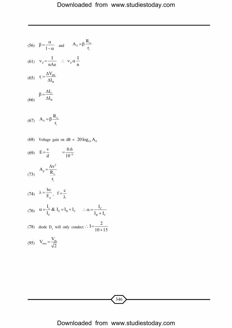
(56) 1
andL
Vi
RAr
(61) dI
nAe d
In
(65)BE
iB
VrI
(66)C
B
II
(67)L
Vi
RAr
(68) Voltage gain on dB = 10 020 log A
(69)vEd
6
0.610
(73)
2
pL
i
AvA Rr
(74)g
hcE
, cf
(76)c
E B CE
I & I I II
C
B C
II I
(78) diode D1 will only conduct 2I
10 15
(95) mrms
VV2
Downloaded from www.studiestoday.com
Downloaded from www.studiestoday.com