unit 1: digital logical circuits
TRANSCRIPT

UNIT 1: DIGITAL LOGICAL CIRCUITSWhat is Digital Computer? OR Explain the block diagram of digital computers.
Digital computer is a digital system that performs various computational tasks. The word “DIGITAL” implies that the information in the computer is represented by
digits. Digital computers use the binary number system, which has two digits, 0 and 1. A binary digit is called a bit. Information is represented in digital computers in the groups of bit. By using various coding techniques, groups of bits can be made to represent not only
binary numbers but also other symbols, letters of alphabets and decimal digit. Bits are grouped together as bytes and words to form some type of representation
within the computer. A sequence of instructions for the computer is known as program.
Block diagram of a digital computer
The hardware of the computer is usually divided into three major parts. The Central processing Unit (CPU) contains an arithmetic and logic unit for
manipulating data, a number of registers for storing data and control circuits forfetching and executing instructions.
The memory of a computer contains storage for instructions and data, it is called aRandom Access Memory (RAM) because the CPU can access any location in memoryat random and retrieve the binary information within a fixed interval of time.
The input and output processor contains electronic circuit for communication andcontrolling the transfer of information between the computer and the outside world.
The input and output device connected to the computer include keyboards, printers,terminals, magnetic disk drives and other communication devices.
What is Gates? Explain the Logic Gates in brief.
Binary information is represented in digital computers using electrical signals. These signals can be represented by voltage to specify one of two possible states. The two states represent a binary variable that can be equal to 1 or 0. The manipulation of binary information in a computer is done using logic circuits called
gates.
Random Access Memory
Central Processing Unit
OutputDevicesInput-Output Processor
InputDevices

Gates are blocks of hardware that produce signals of binary 1 or 0 when input logicrequirements are satisfied.
There are various types of logic gates are commonly used in digital computer. Each gate has a different graphic symbols and operation. The input-output relationship of binary variables for each gate can be represented in
tabular form by Truth-Table. There are three types of gates:
o Basic / Fundamental Gates (AND, OR, NOT)o Universal Gates (NAND, NOR)o Exclusive Gates (EX-OR, EX-NOR)
LOGICAL GATES
Basic / Fundamental Gates Universal Gates Exclusive Gates
(AND, OR, NOT) (NAND, NOR) (EX-OR, EX-NOR)
Basic GatesAND Gate:
In this type of gate output is high only when all its inputs are high. If any single input is law then the output will remain low. So it is said that in AND gate the output is only high when the input is also high.
SYMBOL:
TRUTH-TABLE:
INPUT OUTPUT
A B A AND B0 0 0
0 1 0
1 0 0
1 1 1
OR Gate: In this type of gate if any input signal is high then the output will be high. The output is only low only when all the inputs are low

SYMBOL:
TRUTH-TABLE:
INPUT OUTPUT
A B A OR B0 0 0
0 1 1
1 0 1
1 1 1
NOT Gate: This type of gate is also known as “Inverter”. It is a gate that contains only one input and only one output. The output is always opposite than the input signals.
SYMBOL:
TRUTH-TABLE:
INPUT OUTPUT
A NOT A(A’)
0 1 1 0
Universal Gates
NAND and NOR gates are known as universal gates because we can construct any gate usingNAND & NOR gate.
NOR Gate: The NOR gate is the complement of the OR gate. As shown in the truth table that the output of NOR gate is exactly opposite than the
output of OR gate. This means that the output will be high when all the input is low.
SYMBOL:

TRUTH-TABLE:
INPUT OUTPUT
A B A NOR B0 0 1
0 1 0
1 0 0
1 1 0
NAND Gate: The NAND gate is an AND gate followed by NOT gate. As shown in the truth table that the output of NAND gate is exactly opposite than the
output of AND gate. This means that the output will be high when all the input is high.
SYMBOL:
TRUTH-TABLE:
INPUT OUTPUT
A B A NAND B0 0 1
0 1 1
1 0 1
1 1 0
Exclusive GatesEX-OR Gate:
This gate is produces high output whenever the two inputs are at opposite level. The EX-OR gate is the gate that produces high output for Odd number of high inputs.
SYMBOL:

TRUTH-TABLE:
INPUT OUTPUT
A B A EX-OR B0 0 0
0 1 1
1 0 1
1 1 0
EX-NOR Gate: This gate is produces high output whenever the two inputs are at same level. The EX-OR gate is the gate that produces high output for Even number of high inputs. The truth table shows that output of this gate is exactly opposite of EX-OR gate.
SYMBOL:
TRUTH-TABLE:
INPUT OUTPUT
A B A EX-NOR B0 0 1
0 1 0
1 0 0
1 1 1
Write a note on Boolean Algebra In 1854 George Boole introduced a systemic treatment of logic and developed for this
purpose an algebric system called Boolean Algebra. Boolean Algebra is an algebra that deals with binary variables and logic operations. The variables are designated by letters such as A,B, X ,Y etc. The three basic operations are AND, OR and complement. A Boolean function can be expressed with binary variable, the logic operation
symbols, parentheses ( rounded bracket) and equal to (=) sign. The result of a Boolean function is either 0 or 1.

A Boolean function can be represented by either:
a. Truth tablesb. Logic diagramsc. Algebraic expression
For example: F=x+y’zo F=1 only if x is 1 or if both y’ and z=1.o If y’(complement of y)=1 means that y=0 so we can say that F=1 only when
x=1,y=0,z=1.o So we can say that function F equal to 1 for those combination where x=1 or
yz=01 A Boolean function can be transformed form algebraic expression into a logic diagram
composed of AND,OR and NOT gates. Truth table and logic diagram For above example :
Boolean Operations
There are three basic logical operations:
AND: This operation is represented by a dot or by the absence of an operator. Forexample, x.y = z or xy = z is read “x AND y is equal to z.” The logical operation AND isinterpreted to mean that z=1 if and only if x=1 and y=1; otherwise z=0.
OR: This operation is represented by a plus sign. For example, x+y = z is read “x OR y isequal to z”, meaning that z=1 if x=1 or if y=1 or if both x=1 and y=1. If both x=0 and y=0,then z=0.
NOT: This operation is represented by a prime (sometimes by a bar). For example, x’ =z (or x = z) is read “x not is equal to z”, meaning that z is complement of x. In otherwords, if x=1, then z=0, but if
x=0, then z=1.
Basic Identities of Boolean Algebra
Postulates and theorems of Boolean Algebra
x Y z F
0 0 0 0
0 0 1 1
0 1 0 0
0 1 1 1
1 0 0 1
1 0 1 1
1 1 0 1
1 1 1 1
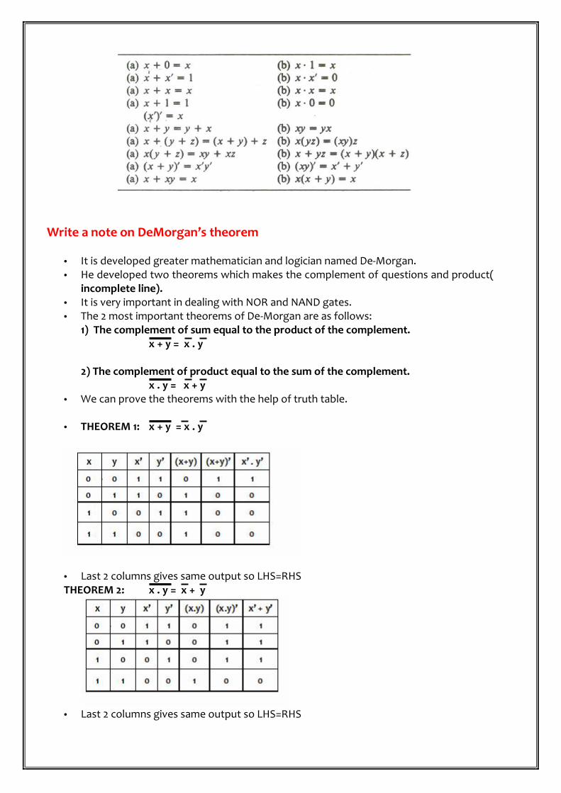
Write a note on DeMorgan’s theorem
It is developed greater mathematician and logician named De-Morgan. He developed two theorems which makes the complement of questions and product(
incomplete line). It is very important in dealing with NOR and NAND gates. The 2 most important theorems of De-Morgan are as follows:
1) The complement of sum equal to the product of the complement.x + y = x . y
2) The complement of product equal to the sum of the complement.x . y = x + y
We can prove the theorems with the help of truth table.
THEOREM 1: x + y = x . y
Last 2 columns gives same output so LHS=RHSTHEOREM 2: x . y = x + y
Last 2 columns gives same output so LHS=RHS

Write a note on K- Maps.
The Karnaugh map is also referred as Veitch Diagrams, KV maps or K-maps. K-map is a method to minimizes the Boolean function. K-map provides a simple and straight forward method to minimizing Boolean
expression. With the help of K-map we can simplified Boolean expression up to 4 and 6 variables. K-map diagram represents squares and each square represents 1 minterm. In K-map values of the variables are written in binary form & the logic function can be
expressed in one of the following formo SUM OF PRODUCTS (SOP)o PRODUCT OF SUM (POS)
A K-map for n variables is made up of 2n squares and each squares designed a productterm of Boolean expression.
For product terms which are present in expression, 1s are written in correspondencesquares and 0 will be written in blank square.
For example: K-map for 2 variables:
F =xy’ + x’y

RULES FOR K- MAP: Each cell with 1 must be included in at list 1 group. Try to form the largest possible groups. Try to end up with as few groups as possible. Groups may be in sizes that are powered of 2. Groups may be square or rectangular only. Groups may be horizontal or vertical but not diagonal. Groups may wrap around the table. Groups may overleap. The larger a group is, the more redundant inputs there are:
o Group of 1 has no redundant input.o Group of 2 known as pair has 1 redundant input.o Group of 4 known as quad has 2 redundant input.o Group of 8 known as octet has 3 redundant input.
Sum-of-Products Simplification A Boolean function represented by a truth table is plotted into the map by inserting 1's
into those squares where the function is 1. Boolean functions can then be simplified by identifying adjacent squares in the
Karnaugh map that contain a 1. A square is considered adjacent to another square if it is next to, above, or below it. In
addition, squares at the extreme ends of the same horizontal row are also considered
adjacent. The same applies to the top and bottom squares of a column. The objectiveto identify adjacent squares containing 1's and group them together.
Groups must contain a number of squares that is an integral power of 2. Groups of combined adjacent squares may share one or more squares with one or
more groups. Each group of squares represents an algebraic term, and the OR of those terms gives
the simplified algebraic expression for the function. To find the most simplified algebraic expression, the goal of map simplification is to
identify the least number of groups with the largest number of members.
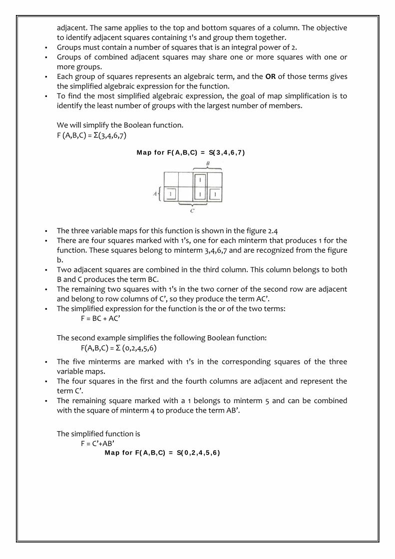
We will simplify the Boolean function.F (A,B,C) = (3,4,6,7)
Map for F(A,B,C) = (3,4,6,7)
The three variable maps for this function is shown in the figure 2.4 There are four squares marked with 1’s, one for each minterm that produces 1 for the
function. These squares belong to minterm 3,4,6,7 and are recognized from the figureb.
Two adjacent squares are combined in the third column. This column belongs to bothB and C produces the term BC.
The remaining two squares with 1’s in the two corner of the second row are adjacentand belong to row columns of C’, so they produce the term AC’.
The simplified expression for the function is the or of the two terms:F = BC + AC’
The second example simplifies the following Boolean function:F(A,B,C) = (0,2,4,5,6)
The five minterms are marked with 1’s in the corresponding squares of the threevariable maps.
The four squares in the first and the fourth columns are adjacent and represent theterm C’.
The remaining square marked with a 1 belongs to minterm 5 and can be combinedwith the square of minterm 4 to produce the term AB’.
The simplified function isF = C’+AB’
Map for F(A,B,C) = (0,2,4,5,6)

Figure 2.6 Map for F(A,B,C,D) = (0,1,2,6,8,9,10)
The area in the map covered by this four variable consists of the squares marked with1’s in fig 1.10. The function contains 1’s in the four corners that when taken as groupsgive the term B’D’. This is possible because these four squares are adjacent when themap is considered with the top and bottom or left and right edges touching.
The two 1’s on the bottom row are combined with the two 1’s on the left of thebottom row to give the term B’C’.
The remaining 1 in the square of minterm 6 is combined with the minterm 2 to give theterm A’CD’.
The simplified function is:F = B’D’ + B’C’ + A’CD’
Product-of-Sums Simplification Another method for simplifying Boolean expressions can be to represent the function
as a product of sums. This approach is similar to the Sum-of-Products simplification, but identifying adjacent
squares containing 0’s instead of 1’s forms the groups of adjacent squares. Then, instead of representing the function as a sum of products, the function is
represented as a product of sums.
ExamplesF(A,B,C,D) = (0,1,2,5,8,9,10)
The 1’s marked in the map of figure 2.7 represents the minterms that produces a 1 forthe function.The squares marked with 0’s represent the minterm not included in F and thereforedenote the complement of F.Combining the squares with 1’s gives the simplified function in sum-of-products form:
F = B’D +B’C’+A’C’D
If the squares marked with 0’s are combined as shown in the diagram, we obtain thesimplified complement function:

F’=(A’+B’)(C’D’)(B’+D)
Figure 2.7 Map for F(A,B,C,D) = (0,1,2,5,8,9,10)
The logic diagram of the two simplified expression are shown in fig 2.8
Logic Diagram with AND and OR gates
The sum of product expression us implemented in fig 2.8(a) with a group of of ANDgates, one for each AND term.
The output of the AND gates are connected to the inputs of a single OR gate. Thesame function is implemented in fig 2.8(b) in product of sum form with a group of ORgates, one for each OR term, the outputs of the OR gates are connected to the inputsof a single And gate.
In each case it is assumed that the input variable are directly available in theircomplement, so inverter are not included.
Write a note on Combinational Circuits
A combinational circuit is the circuit where more than 1 circuit is designed into singlecomponent.
It has N no of inputs and M no of outputs. It is basically used to design digital applications and it transforms the data into the
digital manner. A combinational circuit is a connected arrangement of logic gates with a set of inputs
and outputs.

At any given time, the binary values of the outputs are a function of the binary valuesof the inputs.
The design of a combinational circuit starts from a verbal outline of the problem andends in a logic circuit diagram. The procedure involves the following steps:
1. The problem is stated.2. The input and output variables are assigned letter symbols.3. The truth table that defines the relationship between inputs and outputs is
derived.4. The simplified Boolean functions for each output are obtained.5. The logic diagram is drawn.
Arithmatic circuits: It is made of different arithmetic operators. There will be addition, substraction,
division, modules and any other arithmetic operations.
Half-Adder
Half-Adder is a part of combinational circuit. It is basically designed for arithmetic addition. It is most basic digital arithmetic circuit. Performs the addition of two binary digits. The input variables of a half-adder are called the augend and the addend. The output variables of a half-adder are called the sum and the carry.
Full-Adder
A full-adder performs the addition of three binary digits. Two half-adders can be combined to for a full-adder.. Although a full adder has three inputs, it still only has two outputs since the largest
number is 1+1+1 = 3, and 3 can be represented by two bits.

WHAT IS THE DIFFERENCE BETWEEN HALF ADDER AND FULL ADDER?
Half adder Full adderThe most basic digital arithmetic circuit. A full-adder performs the addition of three
binary digits.Performs the addition of two binary digits. It is used for multi bit additions.Output is sum of two signals. Output is sum of three signals.There are two input and two outputterminal.
There are three input and two outputterminal.
From full adder half adder cant not be built Two full adder makes one full adderOn EX-OR gate and one AND gate are used. Two EX-OR, two AND and one OR gate is
used.

WHAT IS THE DIFFERENCE BETWEEN COMBINATIONAL CIRCUIT ANDSEQUENCIAL CIRCUIT?
COMBINATIONAL CIRCUIT SEQUENTIAL CIRCUIT
It is a digital logic circuit whose outputdepends on the present inputs.
It is a digital logic circuit whose outputdepends on the present inputs as well asprevious inputs.
It can describe by the output values. It can describe by the output values as wellas state values.
It contains no memory element. It contains at least one memory element.
It is easy to design and understand. It is difficult to design and understand.
It is faster in speed. It is slower in speed.
It is expensive in cost. It is less expensive in cost.
Examples of combinational circuit are halfadder and full adder.
Examples of sequential circuit are flip-flopslike RS, Clocked RS, D and JK.
A combinational circuit is a connectedarrangement of logic gates with a set ofinputs and outputs.
However, if a circuit uses both gates andflip-flops, it is called a sequential circuit.
At any given time, the binary values of theoutputs are a function of the binary valuesof the inputs.
Hence, a sequential circuit is aninterconnection of flip-flops and gates.
The design of a combinational circuit startsfrom a verbal outline of the problem andends in a logic circuit diagram.
If we think of a sequential circuit as someblack box that, when provided with someexternal input, produces some externaloutput
What is Flip-flops
A Flip-flop is a binary cell capable of storing one bit of information. It has two outputs, one for the normal value and one for the complement value of the
bit stored in it. Flip-flops are storage elements utilized in synchronous sequential circuits. Synchronous sequential circuits employ signals that effect storage elements only at
discrete instances of time. A timing device called a clock pulse generator that produces a periodic train of clock
pulses achieves synchronization.

Values maintained in the storage elements can only change when the clock pulses. Hence, a flip-flop maintains a binary state until directed by a clock pulse to switch
states. The difference in the types of flip flops is in the number of inputs and the manner in
which the inputs affect the binary state. Flip-flops can be described by a characteristic table which permutates all possible
inputs (just like a truth table). The characteristic table of a flip-flop describes all possible outputs (called the next
state) at time Q(t+1) over all possible inputs and the present state at time Q(t). The most common types of flip flops are:
SR Flip-Flop D Flip-Flop JK Flip-Flop T Flip-Flop
SR Flip-FlopFigure SR Flip-Flop
Inputs: S (for set) R (for reset) C (for clock)
Outputs: Q Q'
The operation of the SR flip-flop is as follow.
If there is no signal at the clock input C, the output of the circuit cannot changeirrespective of the values at inputs S and R.
Only when the clock signals changes from 0 to 1 can the output be affected accordingto the values in inputs S and R
If S =1 and R = 0 when C changes when C changes from 0 to 1 output Q is set to 1. If S =0 and R =1 when C changes from 0 to 1.
If both S and R are 0 during the clock transition, output does not change. When both S and R are equal to 1, the output is unpredictable and may go to either 0
or 1, depending on internal timing that occur within the circuit.

D Flip-FlopD Flip-flop
Inputs: D (for data) C (for clock)
Outputs: Q Q'
The operation of the D flip-flop is as follow.
The D Flip-Flop can be converted from SR Flip-Flop by inserting an inverter between Sand R and assigning the symbol D to the single input.
The D input is sampled during the occurrence of a clock transition from 0 to 1. If D=1, the output of the flip-flop goes to the 1 state, but if D=0, the output of the flip-
flop goes to the 0 state. The next state Q(t+1) is determined from the D input. The relationship can be
expressed by a characteristic equation:Q(t+1) = D
D Flip-Flop has the advantage of having only one input (excluding ), but thedisadvantage that its characteristic table does not have a “no change” conditionQ(t+1) = Q(t).
JK Flip-Flop
Jk Flip-Flop
Inputs: J K C (for clock)

Outputs: Q Q'
The operation of the JK flip-flop is as follow.
A JK Flip-Flop is a refinement of the SR flip-flop in that the indeterminate condition ofthe SR type is defined in the JK type.
Inputs J and K behave like inputs S and R to set and clear the flip-flop, respectively. When inputs J and K are both equal to 1, a clock transition switches the outputs of the
flip-flop to their complement state. Instead of the indeterminate condition of the SR flip-flop, the JK flip-flop has a
complement condition Q(t+1) = Q’(t) when both J and K are equal to 1.
T Flip-Flop
T Flip-Flop
Inputs: T (for toggle) C (for clock)
Outputs: Q Q'
The operation of the T flip-flop is as follow.
Most flip-flops are edge-triggered flip-flops, which means that the transition occurs ata specific level of the clock pulse.
A positive-edge transition occurs on the rising edge of the clock signal. A negative-edge transition occurs on the falling edge of the clock signal. Another type of flip-flop is called a master-slave flip-flop that is basically two flip-flops
in series. Flip-flops can also include special input terminals for setting or clearing the flip-flop
asynchronously. These inputs are usually called preset and clear and are useful forinitialing the flip-flops before clocked operations are initiated.
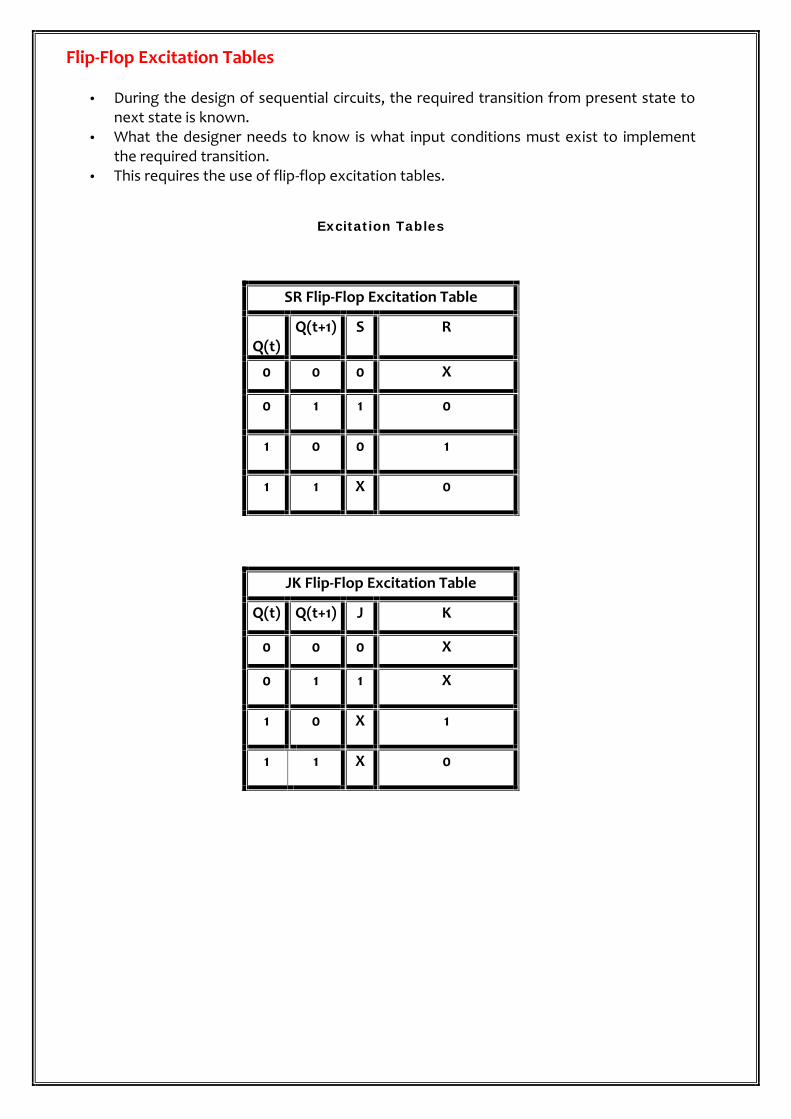
Flip-Flop Excitation Tables
During the design of sequential circuits, the required transition from present state tonext state is known.
What the designer needs to know is what input conditions must exist to implementthe required transition.
This requires the use of flip-flop excitation tables.
Excitation Tables
SR Flip-Flop Excitation Table
Q(t)Q(t+1) S R
0 0 0 X
0 1 1 0
1 0 0 1
1 1 X 0
JK Flip-Flop Excitation Table
Q(t) Q(t+1) J K
0 0 0 X
0 1 1 X
1 0 X 1
1 1 X 0

Sequential Circuits
When a circuit contains just gates, it is called a combinational circuit. However, if acircuit uses both gates and flip-flops, it is called a sequential circuit. Hence, a sequentialcircuit is an interconnection of flip-flops and gates.
If we think of a sequential circuit as some black box that, when provided with someexternal input, produces some external output, a typical sequential circuit wouldfunction as follows:
The external inputs constitute some of the inputs to the combinational circuit. Theinternal outputs of the combinational circuit are the internal inputs to the flip-flops.
The internal outputs of the flip-flops constitute the remaining inputs to thecombinational circuit. The external outputs are some combination of the outputs fromthe combinational circuit and flip-flops. The behavior of a sequential circuit isdetermined from the inputs, the outputs, and the state of the flip-flops. Both theoutputs and the next state are determined by the inputs and the present state.
A state diagram can represent the information in a state table graphically, wherestates are represented by circles (vertices) and transitions on specific input isrepresented by the labels on the directed lines (edges) connecting the circles.
Design Procedure
Formulate behavior of circuit using a state diagram. Determine # of flip-flops needed (equal to # bits in circles). Determine # inputs (specified on edges of diagram). Create state table, assigning letters to flip-flips, input, and output variables.* For each row, list the next state as specified by the state diagram. Select flip-flop type to be used in circuit. Extend state table into an excitation table by including columns for each input of each
flip-flop. Using excitation table and present state-to-next state transitions, formulate input
conditions for flip-flops. Construct truth table for combinational circuit using present-state and input columns
of excitation table (for inputs) and flip-flop inputs (for outputs). Use map simplification of truth table to obtain flip-flop input equations.** Determine external outputs of sequential circuit (flip-flop outputs and potentially
combinational circuit outputs). Draw logic diagram as follows:
T Flip-Flop Excitation Table
Q(t) Q(t+1) T
0 0 0
0 1 1
1 0 1
1 1 0
Draw flip-flops and label all their inputs and outputs. Draw combinational circuit from the Boolean expressions given by the flip-
flop input equations. Connect outputs of flip-flops to inputs in the combinational circuit. Connect outputs of combinational circuit to flip-flop inputs.
For m flip-flops and n inputs, the state table will consist of m columns for the presentstate, n columns for the inputs, and m columns for the next state. The number of rowsin the table will be up to 2m+n, one row for each binary combination of present stateand inputs.
** Each flip-flop input equation specifies a logic diagram whose output must beconnected to one of the flip-flop inputs.
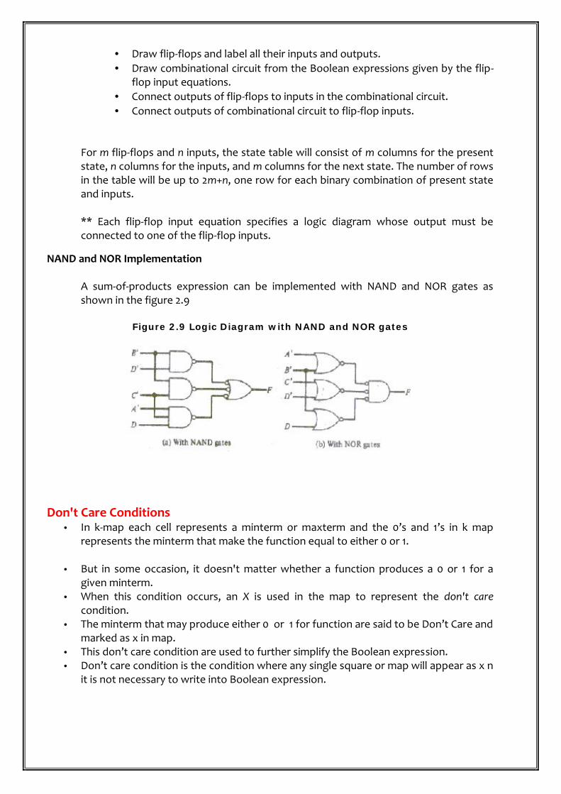
NAND and NOR Implementation
A sum-of-products expression can be implemented with NAND and NOR gates asshown in the figure 2.9
Figure 2.9 Logic Diagram with NAND and NOR gates
Don't Care Conditions In k-map each cell represents a minterm or maxterm and the 0’s and 1’s in k map
represents the minterm that make the function equal to either 0 or 1.
But in some occasion, it doesn't matter whether a function produces a 0 or 1 for agiven minterm.
When this condition occurs, an X is used in the map to represent the don't carecondition.
The minterm that may produce either 0 or 1 for function are said to be Don’t Care andmarked as x in map.
This don’t care condition are used to further simplify the Boolean expression. Don’t care condition is the condition where any single square or map will appear as x n
it is not necessary to write into Boolean expression.

ExampleF(w,x,y,z)= ∑(0,1 ) + d(4,5,14)
So the ans is W’Y’

UNIT 2: DIGITAL COMPONENTS
What is Decoder? Discrete quantities of information are represented in digital computers with binary
codes. A binary code of n bits is capable of representing up to 2n distinct elements of the
coded information. A decoder is a combinational circuit that converts binary information from the n coded
inputs to a maximum of 2n unique outputs. If the n-bit coded information has unused bit combinations, the decoder may have less
than 2n outputs. The decoders presented in this section are called n-to-m-line decoders, where m <= 2n.
Their purpose is to generate the 2n (or fewer) binary combinations of the n inputvariables. A decoder has n inputs and m outputs and is also referred to as an n x mdecoder.
The logic diagram of a 3-to-8-line decoder is shown bellow.
The three data inputs. A0, A1, and A2, are decoded into eight outputs, each outputrepresenting one of the combinations of the three binary input variables.
The three inverters provide the complement of the inputs, and each of the eight ANDgates generates one of the binary combination.
A particular application of this decoder is a binary-to-octal conversion. The inputvariables represent a binary number and the outputs represent the eight digits of theoctal number system.
However, a 3-to-8-line decoder can be used for decoding any 3-bit code to provideeight outputs, one for each combination of the binary code.
Commercial decoders include one or more enable inputs to control the operation ofthe circuit. The decoder of the Figure has one enable input, E.
The decoder is enabled when E is equal to 1 and disabled when E is equal to 0. Theoperation of the decoder can be clarified using the truth table listed in Table.
When the enable input E is equal to 0, all the outputs are equal to 0 regardless of thevalues of the other three data inputs.

The three x's in the table designate don't-care conditions. When the enable input isequal to 1, the decoder operates in a normal fashion.
For each possible input combination, there are seven outputs that are equal to 0 andonly one that is equal to 1.
The output variable whose value is equal to 1 represents the octal number equivalentof the binary number that is available in the input data lines.
Truth Table for 3-to-8-line Decoder
NAND Gate Decoder
Some decoders are constructed with NAND instead of AND gates. Since a NAND gateproduces the AND operation with an inverted output, it becomes more economical togenerate the decoder outputs in their complement form.
A 2-to-4-line decoder with an enable input constructed with NAND gates is shown inFigure.
The circuit operates with complemented outputs and a complemented enable inputE. The decoder is enabled when E is equal to 0. As indicated by the truth table, onlyone output is equal to 0 at any given time; the other three outputs are equal to 1.
The output whose value is equal to 0 represents the equivalent binary number ininputs Ai and Ao.
The circuit is disabled when E is equal to 1, regardless of the values of the other twoinputs.
Decoder Expansion
A technique called decoder expansion can be utilized to construct larger decoders outof smaller ones.

For example, two 2-to-4-line decoders can be combined to construct a 3-to-8-linedecoder. Figure below shows 3-8-line decoder constructed with two 2x4 decoders.
3X8 decoder constructed with two 2X4 decoders
The above given Figure shows how the decoders with enable inputs can be connectedto form a larger decoder.
As you can see that there are two 2-to-4-line decoders are combined to achieve a 3-to-8-line decoder.
The two least significant bits of the input are connected to both decoders. The most significant bit is connected to the enable input of one decoder and through
an inverter to the enable input of the other decoder. It is assumed that each decoder is enabled when its E input is equal to 1. When E is
equal to 0, the decoder is disabled and all its outputs are in the 0 level. When A2 = 0,the upper decoder is enabled and the lower is disabled.
The lower decoder outputs become inactive with all outputs at 0. The outputs of theupper decoder generate outputs Do through D3, depending on the values of A1 andA0(while A2 = 0).
When A2= 1, the lower decoder is enabled and the upper is disabled. The lowerdecoder output generates the binary equivalent D4, through D7 since these binarynumbers have a 1 in the A2 position.

What is Encoder? An encoder is a digital circuit that performs the inverse operation of a decoder. An
encoder has 2n (or less) input lines and n output lines. The output lines generate the binary code corresponding to the input value. An
example of an encoder is the octal-to-binary encoder, whose truth table is givenbelow.
Inputs outputsD7 D6 D5 D4 D3 D2 D1 D0 A2 A1 A00 0 0 0 0 0 0 1 0 0 00 0 0 0 0 0 1 0 0 0 10 0 0 0 0 1 0 0 0 1 00 0 0 0 1 0 0 0 0 1 10 0 0 1 0 0 0 0 1 0 00 0 1 0 0 0 0 0 1 0 10 1 0 0 0 0 0 0 1 1 01 0 0 0 0 0 0 0 1 1 1
The encoder can be implemented with OR gates whose inputs are determined directlyfrom the truth table.
Output A0 =1 if the input octal digit is 1 or 3 or 5 or 7. Similar conditions apply for othertwo outputs.
These conditions can be expressed by the following Boolean functions :A0 = D1 + D3 + D5 + D7A1 = D2 + D4 + D6 + D7A2 = D4 + D5 + D6 + D7
The encoder can be implemented with three OR gates.
Octal-to-binary Encoder
Write a note on Multiplexer
A multiplexer is a combinational circuit that receives binary information from one of 2ninput data lines and directs it to a single output line.
The selection of a particular input data line for the output is determined by a set ofselection inputs. A 2n-to-1 multiplexer has 2n input data lines and n input selectionlines whose bit combinations determine which input data are selected for the output.
The 4-to-1 line multiplexer has six inputs and one output. A truth table describing thecircuit needs 64 rows since six input variables can have 26 binary combinations. This is

an extremely long table and will not be shown here. A more convenient way todescribe the operation of multiplexers is by means of a function table.
The function table for the multiplexer is shown in table. The table demonstrates the relationship between the four data inputs and the single
output as a function of the selection inputs S1 and S0.
Function table for 4-to-1 line multiplexer
Select OutputS1 S0 Y0 0 I00 1 I11 0 I21 1 I3
4-to-1 line Multiplexer
Write a note on DeMultiplexer A decoder with an enable input can function as a demultiplexer. A demultiplexer is a circuit that receives information on a single line and transmits this
information on one of 2n possible output lines. The selection of a specific output line is controlled by the bit values of n selection lines.
The decoder of figure a can function as a demultiplexer if the E line is taken as a datainput line and lines A and B are taken as the selection lines.
The single input variable E has a path to all four outputs, but the input information isdirected to only one of the output lines, as specified by the binary value of the twoselection lines A and B.
For example, if the selection lines AB = 10; output D2 will be the same as the inputvalue E, while all other outputs are maintained at 1.
Because decoder and demultiplexer operations are obtained from the same circuit, adecoder with an enable input is referred to as a decoder / demultiplexer.
It is the enable input that makes the circuit a demultiplexer. Block Diagram for DeMultiplexer

Truth Table Of Demultiplexer
Input OutputD S0 S1 F0 F1 F2 F30 0 0 0 0 0 00 0 1 0 0 0 00 1 0 0 0 0 00 1 1 0 0 0 01 0 0 1 0 0 01 0 1 0 1 0 01 1 0 0 0 1 01 1 1 0 0 0 1
Explain MUX in detail. MUX is combinational circuit that is used to direct one out of 2n input data Lines to A
single output line. It is also known as data selector because it selects one of many inputs And directs it to
the output. The selection of particular input data line is controlled by as Set of selection inputs. Normally there are 2n input data lines and n input selection lines.
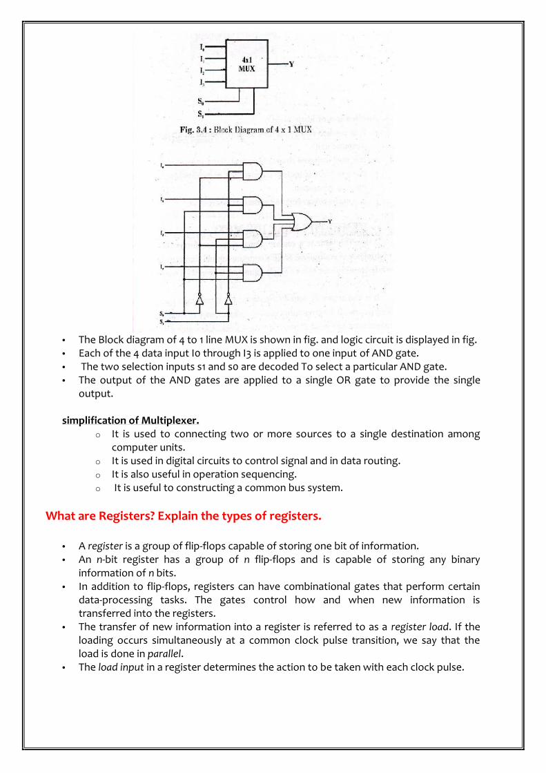
The Block diagram of 4 to 1 line MUX is shown in fig. and logic circuit is displayed in fig. Each of the 4 data input I0 through I3 is applied to one input of AND gate. The two selection inputs s1 and s0 are decoded To select a particular AND gate. The output of the AND gates are applied to a single OR gate to provide the single
output.
simplification of Multiplexer.o It is used to connecting two or more sources to a single destination among
computer units.o It is used in digital circuits to control signal and in data routing.o It is also useful in operation sequencing.o It is useful to constructing a common bus system.
What are Registers? Explain the types of registers.
A register is a group of flip-flops capable of storing one bit of information. An n-bit register has a group of n flip-flops and is capable of storing any binary
information of n bits. In addition to flip-flops, registers can have combinational gates that perform certain
data-processing tasks. The gates control how and when new information istransferred into the registers.
The transfer of new information into a register is referred to as a register load. If theloading occurs simultaneously at a common clock pulse transition, we say that theload is done in parallel.
The load input in a register determines the action to be taken with each clock pulse.
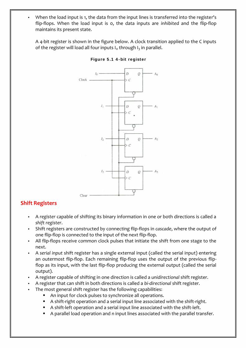
When the load input is 1, the data from the input lines is transferred into the register'sflip-flops. When the load input is 0, the data inputs are inhibited and the flip-flopmaintains its present state.
A 4-bit register is shown in the figure below. A clock transition applied to the C inputsof the register will load all four inputs I0 through I3 in parallel.
Figure 5.1 4-bit register
Shift Registers
A register capable of shifting its binary information in one or both directions is called ashift register.
Shift registers are constructed by connecting flip-flops in cascade, where the output ofone flip-flop is connected to the input of the next flip-flop.
All flip-flops receive common clock pulses that initiate the shift from one stage to thenext.
A serial input shift register has a single external input (called the serial input) enteringan outermost flip-flop. Each remaining flip-flop uses the output of the previous flip-flop as its input, with the last flip-flop producing the external output (called the serialoutput).
A register capable of shifting in one direction is called a unidirectional shift register. A register that can shift in both directions is called a bi-directional shift register. The most general shift register has the following capabilities:
An input for clock pulses to synchronize all operations. A shift-right operation and a serial input line associated with the shift-right. A shift-left operation and a serial input line associated with the shift-left. A parallel load operation and n input lines associated with the parallel transfer.

N parallel output lines. A control state that leaves the information in the register unchanged even
though clock pulses are applied continuously. A mode control to determine which type of register operation to perform.
The simplest possible shift register is one that uses only flip-flops, as shown in thefigure below.
4-bit shift register
Bidirectional Shift Register with parallel load
A register that can shift in both directions is called a bi-directional shift register. A 4-bit bidirectional shift register with parallel load is shown in figure below. Each
stage consists of a D flip-flop and a 4X1 MUX. The two selection inputs S1 and S0 select one of the MUX data inputs for the D flip-
flop. The selection lines control the mode of operation of the register according to thefunction table shown in table below.
When the mode control S1S0 = 00, data input 0 of each MUX is selected. This condition forms a path from the output of each flip-flop into the input of the
same flip-flop. The next clock transition refers into each flip-flop the binary value it held previously,
and no change of state occurs. When S1S0 = 01, the terminal marked 1 in each MUX hasa path to the D input of the corresponding flip-flop.
This causes a shift-right operation, with the serial input data transferred into flip-flopA0 and the content of each flip-flop Ai-1 transferred into flip-flop Ai for i=1,2,3. WhenS1S0 = 10 a shift-left operations results, with the other serial input data going into flip-flop A3 and the content of flip-flop Ai+1 transferred into flip-flop Ai for I=0,1,2. WhenS1S0 = 11, the binary information from each input I0 through I3 is transferred into thecorresponding flip-flop, resulting in a parallel load operation.
In the diagram, the shift-right operation shifts the contents of the register in the downdirection while the shift left operation causes the contents of the register to shift inthe upward direction.
Bidirectional Shift register with parallel load

Application of Shift Registers
Shift registers are often used to interface digital systems situated remotely from eachother. For example, suppose that it is necessary to transmit an n-bit quantity betweentwo points.
If the distance between the source and the destination is too far, it will be expensiveto use n lines to transmit the n bits in parallel.
It may be more economical to use a single line and transmit the information seriallyone bit at a time.
The transmitter loads the n-bit data in parallel into a shift register and then transmitsthe data from the serial output line.
The receiver accepts the data serially into a shift register through its serial input line.When the entire n bits are accumulated they can be taken from the outputs of theregister in parallel.
Thus the transmitter performs a parallel-to-serial conversion of data and the receiverconverts the incoming serial data back to parallel data transfer.

UNIT 3: DATA REPRESENTATION
What is Number System? A number system is a set of numbers, together with one or more operations such as
addition or multiplication. There are mainly two types of number system
o Positional number systemo Non positional number system
NON POSITIONAL NUMBER SYSTEMo In this system each symbol represents the same value so it is difficult to
perform arithmetic operation with such numbers. POSITIONAL NUMBER SYSTEM
o In this system each number is identified by the position where it is placed. Itmeans that the value of number is depended on the position. In this kind ofsystem it is possible to perform the arithmetic operation very easily.
o There are mainly 4 types of positional number systems are commonly used. Binary Octal Decimal HexaDecimal
Binary Number Systemo This number system is used in computers or digital systemso 1.o Each digit enter in the system is represented in the form of 0 and 1s
Octal Number Systemso in this system there are 8 different characters are used to represent the
numbers.o We can use 0 to 7 different symbols are used.o In octal number system base is 8o In this number system values increase from right to left as 1, 8, 64, 512, 4096..
Decimal Number Systemo in this system there are 10 different characters are used to represent the
numbers.o We can use 0,1,2,3,4,5,6,7,8,9 different symbols are used.o In octal number system base is 10.o In this number system each positions of number is given depending on weight.o For example: 4123
=4 * 103 + 1 * 102 + 2 * 101 + 3 * 100
=4 * 1000 + 1 * 100 + 2 * 10 +3 * 1=4000+100+20+3=4123
HexaDecimal Number Systemo This system is very useful in microprocessoro There are 16 different characters are used to represent the numbers.o We can use 0,1,2,3,4,5,6,7,8,9 and A,B,C,D,E,F different symbols are used.o The values are increases from right to left of hexadecimal points as 1, 16, 256,
65536 and so on.

ConversionsConverting Decimal To Binary
o In conversion from decimal to any other number system, the steps to befollowed are:
o Divide the decimal number by the base of 2.o Note the remainder in one column and divide the quotient again with the base.
Repeat this process until the quotient is reduced to a zero.o Example: The decimal number is 65
2 65 12 32 0 2 16 02 8 02 4 02 2 0
1 The binary number of 65 is 1000001
Converting Binary To Decimalo The decimal number of 100001 iso = (1*26)+(0*25)+(0*24)+(0*23)+(0*22)+(0*21)+(1*20)o = (1*64) + (0*32) + (0*16) + (0*8) + (0*4) + (0*2) + (1 * 1)o = 64 + 0 + 0 + 0 + 0 + 0 + 1o = 65o The decimal number of 1000001 is 65
Octal Number System (Base 8)o A commonly used positional system is the Octal System. The octal system has a
base of 8.o The values increase from left to right as 1, 8, 64, 512, 4096,….
Converting Decimal To Octalo In conversion from decimal to any other number system, the steps to be
followed are:o Divide the decimal number by the base of the 8.
Example: The decimal number is 224
8 224 08 28 4 8 3 3
The octal number of 224 is 340Converting Octal To Decimal
o The octal number is 340o = (3*82)+(4*81)+(0*80)o = (3*64) + (4*8) + (0*1)o = 192 + 32 + 0o = 224o The decimal number of 340 is 224

Converting Binary Octal000 0
001 1 010 2 011 3
100 4
101 5
110 6 111 7
Converting from Binary to Octalo The binary number must be divided into groups of three from the octal point –
to the right in case of the fractional portion and to the left in case of theinteger portion. Each group can then be replaced with their octal equivalent.
o Exampleo Binary 101010101010100o 101 010 101 010 100o 5 2 5 2 4o So, 52524 is the Octal equivalent of binary 101010101010100
Converting Octal to Binaryo Each octal digit is replaced with the appropriate ‘triple’ of binary digits.o e.g. 65o 5o 110 101o The binary equivalent of the Octal number 65 is 110101
Hexadecimal Number System (Base 16)o There is another commonly used positional system, hexadecimal system.o The hexadecimal system has a base of 16, so the value increases from left to
right as 1, 16, 256, 65536,. . . .o We need to keep a simple table in mind before we attempt any conversion
from hexadecimal or vice-versa.Converting Decimal To HexaDecimal
o In conversion from decimal to any other number system, the steps to befollowed are:
o Divide the decimal number by the base of 16.Example:
The decimal number is 37016 370 216 23 716 1 1
0 The hexadecimal number of 370 is 172
Converting Hexadecimal To Decimalo The hexadecimal number 172o = (1*162) + (7*161) + (2*160)o = (1*256) + (7*16) + (2*1)o = 256+112+2o = 370

o The decimal number of 172 is 370Converting Binary to Hexadecimal
o Each hexadecimal digit is represented by 4 binary digits.Binary Hexadecimal
0000 00001 10010 20011 30100 40101 50110 60111 71000 81001 91010 A1011 B1100 C1101 D1110 E1111 F
o To convert a binary number to its hexadecimal equivalent we split the quantityinto groups of four onwards, as before.
o Each of this group of four is directly converted into their hexadecimalequivalent.
o We may add zeros to the left of the number if necessary.o exampleo Binary 10101011000010o 0010 1010 1100 0010o 2 A C 2o So, the hexadecimal equivalent of binary 10101011000010 will be 2AC2
Converting Hexadecimal to Binaryo The conversion from hexadecimal to binary consists of writing off the binaryo Equivalent of each hexadecimal digit in groups of four.o e.g.o Hexadecimal 1901A0412Co 0001 1001 0000 0001 1010 0000 0100 0001 0010 1100o 1 9 0 1 A 0 4 1 2 Co Thus the required binary number can be written as:o 1100100000001101000000100000100101100
Converting Hexadecimal to Octalo Write 4 digit binary numbers for each hexadecimal.o Arrange the entire number sequence into group of 3 bit section.o If any bit is missing add 0 on leftmost section.o Now write down octal equivalent of each 3 bit section.o Example:o The hexadecimal number is 2A35.o 2 A 3 5o 0010 1010 0011 0101
000 010 101 000 110 101

o 0 2 5 0 6 5o The octal number is 25065
Converting Octal to Hexadecimalo Write 3 digit binary number for each octal.o Arrange the entire number sequence into group of 4 bit section.o If any bit is missing add 0 on leftmost section.o Now write down hexadecimal equivalent of each 4 bit section.o Example:o The octal number is 25065.o 2 5 0 6 5o 010 101 000 110 101o 0010 1010 0011 0101o 2 A 3 5o The hexadecimal number is 2A35
Binary Arithmetico All the arithmetic operations are possible in binary numbering system like
addition, subtraction, multiplication and division All the Arithmetic operationsare done in binary number system are explained as under:
Additiono For binary addition the following rules of binary addition are to be considered:
input
A B
Sum of A + B Carry
0 0 0 0
0 1 1 0
1 0 1 0
1 1 0 1
o e.g. 1 Add two binary numbers 11011 and 111 Carry 1 1 1 1
1 0 1 1 1 + 1 1 1
1 0 0 0 1 0 (Answer)Subtraction
o Binary substraction is just similar as we perform substraction on decimalnumbers.
o Though there are other methods of performing subtraction, we will considerthe method of subtraction know as complementary subtraction.
o To perform substraction we must have to follow the following rules:input
A B
Subtraction of A B
borrow
0 0 0 0
0 1 1 1
1 0 1 0
1 1 0 0

Multiplicationo Multiplication in binary follows the same rules that are followed in the decimal
system. The table to be remembered is:
input
A B
Multiplication ofA * B
0 0 0
0 1 0
1 0 0
1 1 1
e.g. : 1010 * 10011010
x 1001
1010 0000
0000 1010
101101 0 The answer is (1011010)
DivisionTable for binary division is given as under:
input
A B
Division of A / B
0 0 Undefined
0 1 0
1 0 Undefined
1 1 1
o The steps for binary division are:o Start from the left of the dividend.o Perform subtraction in which the divisor is subtracted from the dividendo If subtraction is possible put a 1 in the quotient and subtract the divisor from
the corresponding digits of the dividend else put a 0 in the quotiento Bring down the next digit to the right of the remainder.o Execute step 2 till there are no more digits left to strating down from the
dividend.

o e.g.o 100001 / 110
0101 (quotient)110 100001
110 1000 110 100 110 1001 110 11 (reminder)
Write a note on Floating Point Representation. A number which has both an integer part as well as fractional part is called Real or
Floating point Number. For e.g. 2.365, 78.738789, 6.5643 etc are the examples of floating point numbers. The floating point representation of numbers has two pars.
sign Fixed pointMantissa
Exponent
The first part represents a sign fixed point number called Mantissa. The second part designated the position of decimal or binary point; this part is known
as exponent. The fixed point mantissa may be integer or fractional. For example : the decimal no +6132.789 is represent in floating point with exponent
and fraction as follows:
sign Fixed pointMantissa
Exponent
+ 0.6132789 04
The value of exponent indicates that the actual position of decimal point is 4 positionsto the right of the indicated decimal point in the fraction.
We can also represent this number as +0.6132789 × 10⁴ like scientific notation. In general floating point is represented in the form of m × re. where
m = mantissar = radixe = exponent.
In above example 6132789 is mantissa, 4 is exponent and 10 is radix.

Write a note on Error Detection Code. OR what do you mean by parity? Explainit with error detection code.
An error detection code is a binary code that detects error during informationtransmission.
The error detection code can not be correct error but gives just indication that theerror is presents.
There are various techniques to detect error but the most common is parity bit.
Parity Bit
A parity bit is an extra bit included with a binary message to make the total number of1’s either odd or even.
Generally there are 2 techniques even and odd parity is used. In even parity bit the sum of all 1’s is even while in odd parity the sum of all 1’s is odd. For e.g. for three bit message has two possible parity shown in bellow table.
MessageXyx
P(odd) P(even)
000 1 0
001 0 1
010 0 1
011 1 0
100 0 1
101 1 0
110 1 0
111 0 1
During transformation of information from one location to another parity bit is handleas follows:
o At sending end, the message transferred to parity generator.o The parity generator generates required parity.o Then the message transferred to destination.o At destination the parity checker checks the proper parity adopted.o An error is detected if the checked parity doesn’t confirm to the adopted
parity. The parity generator & checker network are logic circuits constructs with Exclusive or
gate.

UNIT 4: CENTRAL PROCESSING UNITWrite a note on Central Processing Unit.
The central processing unit is the brain of digital computer. It performs various types of function depending on the instruction that incorporated
in the computer. The main function of the central processing unit is to execute the programs and
generates the results, except that it also controls the internal and external parts of thecomputers.
The control unit, register sets and ALU are the major three components of centralprocessing unit.
The main memory is also a part of central processing unit. The CPU of small computer contains a single microprocessor while the CPU of large
computer may contain multiple microprocessors. The microprocessor contains two major parts that is CU – Control Unit and ALU –
Arithmetic and Logical Unit. Control Unit: it controls the entire operations of the system. It also controls the input
and output devices. Arithmetic & Logical Unit: it performs the mathematical as well as logical operations
on the instruction. This unit is responsible to generate the output on inputtedinstructions.
Register sets: the register sets contain more than one registers. The registers arebasically used for storing immediate results during the process of executinginstruction. Various registers performs various task.
CU
REGISTER SET
ALU

Explain General Register Organization.
The set of registers in a computer are connected to the ALU using busses andMultiplexers.
A 14-bit control word specifies two source registers (SELA & SELB), a destinationregister (SELD), and an operation (OPR).
The registers can be specified using three bits each as follows:
A bus organization for seven CPU registers is shown in fig. The output of each Register Connected to two multiplexers to perform the two buses
A and B. The selection lines in each multiplexer select one register of the input data for the
particular logic unit (ALU). The operation selected in the ALU determines the arithmetic or logic micro operations
that are to be performed. The result of the micro-operation is available for output data and also goes into the
inputs of all the registers. The register that receives the information from the output bus is selected the
decoder.

The decoder activates one of the register load inputs, thus providing a transfer Pathbetween the data in the output bus and the inputs of the selected destination register.
The control unit that operates the CPU bus system directs the information flowthrough the registers and ALU selecting the various components in the system.
SHORT NOTE: CONTROL WORD
There are 14 – bit binary selection input in the unit and their combine value that specifya control word.
The figure of 14 – bit combine word is as given below:
SELECTIONA
SELECTION B SELECTION D OPR
3 bit 3 bit 3 Bit 5 bit In this 14 – bit combine word, first 3 columns contains 3 bits and last column contain 5
bits. The first field is a SELECTION A that contains 3 bits The second field is a SELECTION B that contains 3 bits The third field is a SELECTION D that contains 3 bits The last field is a OPR that contains 5 bits The 3 bits of SELECTION – A, SELECTION – B and SELECTION – D that selects a source
register for the input of the ALU The 5 bits of OPR that selects a destination register for output of the ALU
WHAT IS INTERRUPT? EXPLAIN IN DETAIL.
The concept of program interrupt is use to handle variety of problems that arrives outof normal program sequence.
The interrupt facility is useful in multi programming Environment when two or moreprogram resided in the memory at same time.
The function of interrupt facility is to take care of data transfer of one or moreprogram while another program is currently being executed.
TYPES OF INTERRUPT :
There are three major type of interrupt.o External interrupt :o Internal interrupt:o Software interrupt
External interrupt :
o The external interrupt caused by external events, they comes from Inputoutput devices, timing devices, timing devices of power supply or any otherExternal sources.
o The external interrupt are asynchronous and they are independent of Theprogram being executed at the time.
Internal interrupt:

o Internal interrupt is generated by some exceptional condition that cause by theprogram itself.
o This type of interrupt arises from illegal or erroneous use of an Instruction ordata. It is known as traps.
o Examples that cause the internal interrupts are register overflow, stackoverflow, etc.
o This interrupt are synchronous with program. If the program is rerun theinternal interrupts will occur in the same place each time.
Software interrupt
o Software interrupts is initiated by executing an instruction.o Software Interrupt is a special call instruction that behave like an interrupt
rather then subroutine Call.o The most common use of this interrupt is associated with supervisor switching
from CPU. User mode to the supervisor mode.o When input-output transfer is required the supervisor mode is requested by
means of supervisor call instruction.
WHAT IS STACK ORGANIZATION? EXPLAIN THE TYPES OF STACKORGANIZATION.
A stack is an ordered set of elements only one of which can be used at a time The point of access is called top of the stack The number of elements in the stack or length of the stack is a variable The items may be added to or deleted from the top of the stack as Push Down list or
Last In First Out (LIFO) List A useful feature that is included in the CPU of most computer is stack or Last In First
Out (LIFO) List A stack is a storage device that stores information in such a manner that the item
stored last is the first item retrieved. The register that holds the address for the stack is called a Stack Pointer (SP) because
its value always points at the top item in the stack The two operation of stack are PUSH and POP The operation of insertion is called PUSH The operation of deletion is called POP
TYPES OF STACK OPERATION
There are two types of stack operation like REGISTER STACK & MEMORY STACK
REGISTER STACK
A stack can be placed in a portion of a large memory or it can be organized as acollection of a finite number of memory words or registers
Register stacks organized the operation from each and every word and its operationinto the memory in register stack operation

The stack pointer (SP) register contains 4 binary numbers whose value is equal to theaddress of the word that is currently on top of the stack
The fig shows the organization of 64 words registerstack. As shown in figure
Three items are place in stack that is x, y and z item is top of the stack. So that SP is now 3.
SP means Stack pointer. DR means Data Register There are two types of operations are used in this type of Register Stack Operation
like PUSH and POP
PUSH
If the stack is not full then a new item is inserted with a push operation If the stack is full and user tries to insert a new value in the stack then it is called Stack
Overflow error.
POP
A new item is deleted from the stack if the stack is not empty. If the stack is empty and user tries to delete an item from the stack then it is called
Stack Underflow error.
MEMORY STACK
A stack exist as a stand alone unit or it can be implemented in RAM that attached toCPU
There are three types of segments are used in the memory stack like Program, Dataand Stack.
The Program Counter (PC) points at the address of the next instruction in the program The address Register (AR) points at an array of data The Stack Pointer (SP) points at the top of the stack This type of three segments are connected with the common address bus There are two types of operations are used in this type of Memory Stack Operation
like PUSH and POP
PUSH
ZYX
FULL EMPTY
SP
ADDRESS
63
43210

If the memory is not full then a new item is inserted with a push operation If the memory is full and user tries to insert a new item in the memory then it is called
Memory Overflow error or Full Memory error.
POP
A new item is deleted from the memory if the memory is not empty. If the memory is empty and user tries to delete an item from the memory then it is
called Memory Underflow error or Empty Memory error.
SHORT NOTE: REVERSE POLISH NOTATION
Evaluating ordinary arithmetic expressions using a computer is difficult, particularlywhen an Expression consists of parenthesis and brackets.
In this case an expression has to be scanned from Left as well from the right. These problems arise because in an ordinary arithmetic expression operator is placed
in between the two operands. Such types of ordinary expressions are called Infixexpression.
To overcome this problem the polish mathematician Lukasi showed that a ArithmeticExpression can be represented in prefix or postfix Notation.
In prefix notation (also known as Polish notation) the operator is placed before theoperands while in postfix notation (also known as Reverse polish notation, RPN) theoperator is placed after the operands.
In short arithmetic expression can be represented in three different way as follows.
A+B : INFIX NOTATION +AB : PREFIX OR POLISH NOTATION AB+ : POSTFIX OR REVERSE POLISH NOTATION (RPN)
RPN has number of advantages over infix notation for expressing algebraic formulas. Any formula can be expressed without parenthesis. It is convenient for evaluating formulas on computer with stack. The infix operator has precedence which is undesirable. This disadvantages is eliminated By reverse polish notation. The main advantage of polish notation is that any formula can be expressed without
Parenthesis. This is possible by combining reverse polish notation with a stack registers. Hence stack is very useful for handling long and complex problems involving
arithmetic Expressions. This procedures is employed in some electronic calculators and computers. In this method The arithmetic expressions first converted reverse polish notation and
then operands are pushed Into the stack in the order in which they appear. Let us discuss one example for more clarification of this procedure. Consider
arithmetic Expression. (6*3) + (5*9) In reverse polish notation it is expressed as 36*95*+
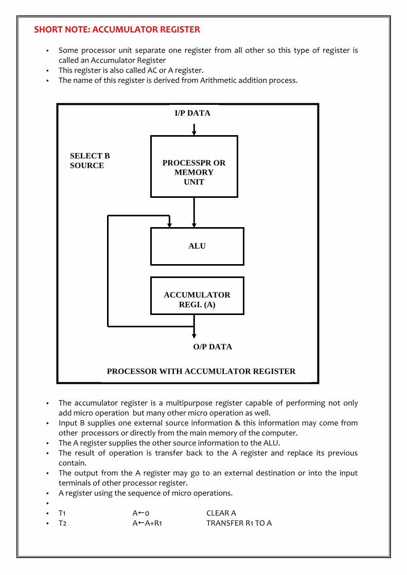
SHORT NOTE: ACCUMULATOR REGISTER
Some processor unit separate one register from all other so this type of register iscalled an Accumulator Register
This register is also called AC or A register. The name of this register is derived from Arithmetic addition process.
The accumulator register is a multipurpose register capable of performing not onlyadd micro operation but many other micro operation as well.
Input B supplies one external source information & this information may come fromother processors or directly from the main memory of the computer.
The A register supplies the other source information to the ALU. The result of operation is transfer back to the A register and replace its previous
contain. The output from the A register may go to an external destination or into the input
terminals of other processor register. A register using the sequence of micro operations. T1 A0 CLEAR A T2 AA+R1 TRANSFER R1 TO A
PROCESSPR ORMEMORY
UNIT
I/P DATA
ALU
ACCUMULATORREGI. (A)
O/P DATA
SELECT BSOURCE
PROCESSOR WITH ACCUMULATOR REGISTER

T3 AA+R2 ADD R2 TO A. Register A is first cleared then first number. In R1 is transferred into the accumulator register (A) by adding it to the present zero
content to A. The second number in R2 is then added to the present value of A. The sum formed in A may be used for other computations or may be transferred to a
required destination.
SHORT NOTE: INPUT – OUTPUT PROCESSOR (IOP)
An Input – Output Processor (IOP) is a software program that is used to control input– output operations
An Input – Output Processor (IOP) controls sending and receiving data between Input– Output Process
An Input – Output Processor (IOP) finds and corrects sending and receiving errorsbetween Input – Output Process
An Input – Output Processor (IOP) assembles and disassembles messages betweenInput – Output Process
An Input – Output operation is performed by the CPU
In figure, we can show that, Memory bus contains CPU and IOP for communication Input / Output bus (I / O) Bus is connected with the Input – Output Processor (IOP)
with the help of Peripheral devices (PD). An Input – Output Processor (IOP) communicates with the peripheral device through
the I/O bus and with the memory through the memory bus. When IOP needs to transfer data to or from memory, it starts a memory cycle from the
CPU and then it transfers the data to or from memory. In computer, CPU is the master processor and IOP is slave processor. CPU sends information by using IOP path.

IOP contains status word into that memory location. CPU checks the status word if the status word is correct then CPU inform to the IOP
about sending information. After that, IOP reads and executes commands from the memory that located at the
specified location. When the IOP completes the Input Output data transfer then it informs to the CPU for
data transfer is completed.

UNIT 5: INPUT OUTPUT ORGANIZATIONWRITE A NOTE ON MEMORY BUSES.
A collection of cables through which is transmitted from one peripherals devices intoanother peripherals devices that is known as Bus
Buses can send the data information, address information, special instruction fromone device into another device.
There are many types of buses are used likeo Internal buso External buso System buso Instruction buso Memory buso Data buso Address buso Control buso Input output bus
Internal Bus Internal bus is placed inside the processor. Internal bus is used to send information between processor register and internal
components of processorExternal Bus External bus is placed outside the processor. External bus is used to send information between one parts of computer into another
part of computerSystem Bus System bus is used to connect the processor with main memory Instruction Bus Instruction bus is used to fetch the instruction from main memoryMemory Bus Memory bus is used to carry memory location. Memory bus is used to connect system memory with the processorData Bus Data bus is used to send data from one parts of computer into another part of
computer Data bus is used to send data to the processor, memory and other parts of computers Data bus is used to connect the processor, memory and other parts of computers for
communicate with each other for transferring the dataAddress Bus Address bus is used to send address from one parts of computer into another part of
computer Address bus is used to send address to the processor, memory and other parts of
computersControl Bus Control bus is used to control the data and information of the data bus and address
busInput – Output Bus Input – Output bus is used to connect between processor and input – output parts for
data transmission.

Input – Output bus contains data line, address line and control line for datatransmission
SHORT NOTE: DMA OR DMA CONTROLLER
DMA means Direct Memory Access. DMA is a process of communication or data transfer that controlled by an external
peripheral. When the DMA is used in the memory, the microprocessor controlled the data
transfer. For 8085 microprocessor, HOLD and HLDAC signal use for this type of data transfer. Direct memory access is an input output technique for fast data transfers. Direct memory access (DMA) allows hardware system for reading or writing process
of the central processing unit. Many hardware systems use DMA including Disk drive controllers, graphics cards,
network cards and sound cards. The data transfer speed of Central processing unit is limited between secondary
memory and Main memory. This problem can be resolved by removing CPU from the path. After Removing CPU, different peripheral manages the memory buses directly for the
improvement of data transfer rate. This special kind of method is known as DirectMemory Access (DMA).
In this type of DMA process, When Input device needs to transfer data to or frommemory, it request to the DMA controller by setting DMA Bus Request Input to 1 andDMA Bus Grant Input to 1.
Here 1 means Enable and 0 means Disable Bus Request (BR) is used to pass the request to the CPU. After that, CPU accept the request from the Bus Request (BS) signal when the Bus
Grant (BG) is Enable. After that, CPU can read and write the request by using Read (RD) and Write (WR)
signal.
Data Bus
Address Bus
Read
Write
HighImpendence(Disable)When BG IsEnable
D Bus
A Bus
RD
WR
BR
BG
DMA Transfer
Bus Request
Bus Grand

After that CPU gives address into that request by using Address Bus (A BUS) and alsogive data into that request by using Data Bus (D BUS).
After that CPU can transfer to that request from one place into another by using DMAcontroller.
When data transfer is completed then Bus Request and Bus Grant signal becomesdisable.
DMA method allows the Input / Output devices to directly communicate with the mainmemory of a computer.
DMA method directly reads and writes data from the memory by using memory bus DMA is a technique for moving data directly between main memory and peripheral of
computer without need of CPU DMA Controller contains 3 types of register like Address Register, Word Count
Register and Control Register.
ADDRESS REGISTER
Address register contains the address of memory where the data from the inputdevice needs to be stored or from where the data for the output device needs to befetched
CPU gives this address to the data bus. The address is transferred to the Address Register from the Data Bus through the
Internal Bus. Address in this register is incremented after transferring each word to or from
memory
WORD COUNT REGISTER
Word Count Register stores the number of words the need to be read from or writteninto memory
It is decremented after each word transfer. When the value in this register becomes zero, it is assumed that data transfer has
completed
CONTROL REGISTER
The control register specifies the mode of data transfer like it is a read operation or itis a write operation
CPU reads the data through the data bus after setting to Read Input to 1 CPU writes the data through the data bus after setting to Write Input to 1