#04-2021-1000-104 lecture2 combinational logical circuits i
TRANSCRIPT

20.01.21 11:56
CSCI 150 Introduction to Digital and Computer
System Design Lecture 2: Combinational Logical Circuits I
Jetic Gū
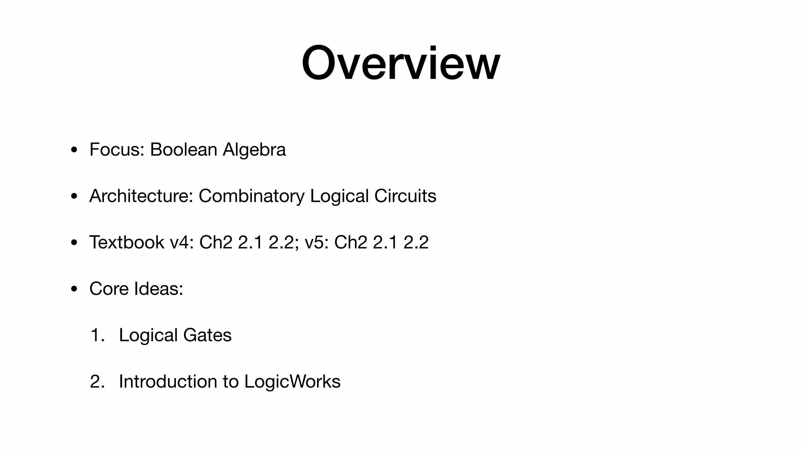
Overview• Focus: Boolean Algebra
• Architecture: Combinatory Logical Circuits
• Textbook v4: Ch2 2.1 2.2; v5: Ch2 2.1 2.2
• Core Ideas:
1. Logical Gates
2. Introduction to LogicWorks

Logic Gates
Summary
P1 Logic Gates
And, Or, Not Gates, LogicWorks

What is a Logic Gate?
• A basic circuit unit implemented using transistors and interconnections
• We when analysing a digital circuit, are not concerned with the internals of a gate, but only it’s external properties
• Performs a single logical operationoperate on one or more binary input signals to produce an output signal
Concep
t
P1 Logic Gates

What is a Logic Gate?
Concep
t
P1 Logic Gates
• Similar to in electric circuit design, we are not concerned with the design of the lightbulb or battery, but we know what it does.
• A logic gate is like that, we know it’s external logic properties, that’s enough.

First 3 Gates
Concep
t
P1 Logic Gates
Z = X ⋅ YXY
Z = X + YXY
Z = XX
AND Gate
OR Gate
NOT Gate

First 3 Gates
Concep
t
P1 Logic Gates
Z = X ⋅ YXY
Z = X + YXY
Z = XX
AND Gate
OR Gate
NOT Gate
Input

First 3 Gates
Concep
t
P1 Logic Gates
Z = X ⋅ YXY
Z = X + YXY
Z = XX
AND Gate
OR Gate
NOT Gate
Input Output

AND Operator and Boolean Algebra / Binary Logic
Concep
t
P1 Logic Gates
Z = X ⋅ YXY
• AND: is equal to AND
• Operator: (\cdot)
Z X Y
⋅
• Boolean Algebra
• Each variable can only have one of two values:
• TRUE/ON/1
• False/OFF/0

AND Operator and Boolean Algebra
Concep
t
P1 Logic Gates
Z = X ⋅ YXY
AND Truth Table
0 0 0
0 1 0
1 0 0
1 1 1
Z = X ⋅ YYX
• AND: is equal to AND
• Operator: (\cdot)
Z X Y
⋅
• Truth Table
• Left: all combinations of input values
• Right: corresponding output values

OR Operator
Concep
t
P1 Logic Gates
OR Truth Table
0 0 0
0 1 1
1 0 1
1 1 1
Z = X + YYX• OR: is equal to or
• Operator:
Z X Y
+
Z = X + YXY

NOT Operator
Concep
t
P1 Logic Gates
NOT Truth Table
0 1
1 0
Z = XX
• NOT: is equal to NOT
• Operator: (\overline{X})
• Also called: Complement operation; Inverter gate
Z X
X
Z = XX
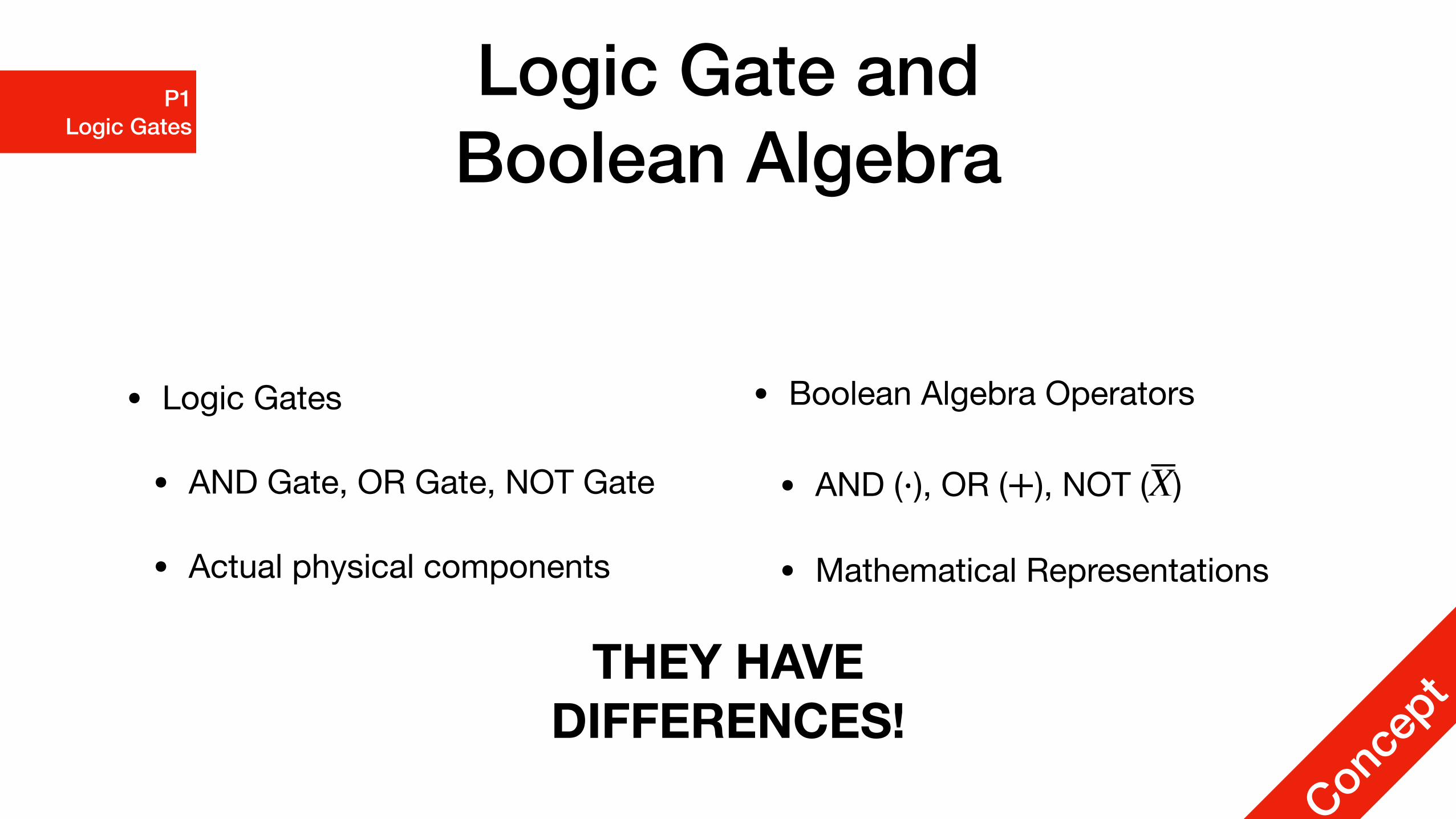
Logic Gate and Boolean Algebra
• Logic Gates
• AND Gate, OR Gate, NOT Gate
• Actual physical components
Concep
t
P1 Logic Gates
• Boolean Algebra Operators
• AND ( ), OR ( ), NOT ( )
• Mathematical Representations
⋅ + X
THEY HAVE DIFFERENCES!

Digital Logical Gates• In math, everything happens simultaneously
• An equation like doesn’t change with time/location
• In digital circuits, we have electrons as 'messengers'. They travel at about 2,200 kilometres per second
• Logic gates are tiny circuits, which means they still have internal components: even slower
• This means: there will be tiny delays called Gate Delay
250 + 760 = 1010
Tech
nical
P1 Logic Gates
Digital Logical Gates
Tech
nical
P1 Logic Gates
Timing Diagram
Z = X ⋅ YXY
1
X1
Y1
0 1 2 3 4 5
Z

Digital Logical Gates
Tech
nical
P1 Logic Gates
Timing Diagram
Z = X ⋅ YXY
1
X1
Y1
0 1 2 3 4 5
Z
0 1 0 1 0

Digital Logical Gates
Tech
nical
P1 Logic Gates
Timing Diagram
Z = X ⋅ YXY
1
X1
Y1
0 1 2 3 4 5
Z
0 1 0 1 0
0 0 1 1 0

Digital Logical Gates
Tech
nical
P1 Logic Gates
Timing Diagram
Z = X ⋅ YXY
1
X1
Y1
0 1 2 3 4 5
Z
0 1 0 1 0
0 0 1 1 0
transition transition

Digital Logical Gates
Tech
nical
P1 Logic Gates
Timing Diagram
Z = X ⋅ YXY
1
X1
Y1
0 1 2 3 4 5
Z
0 1 0 1 0
0 0 1 1 0
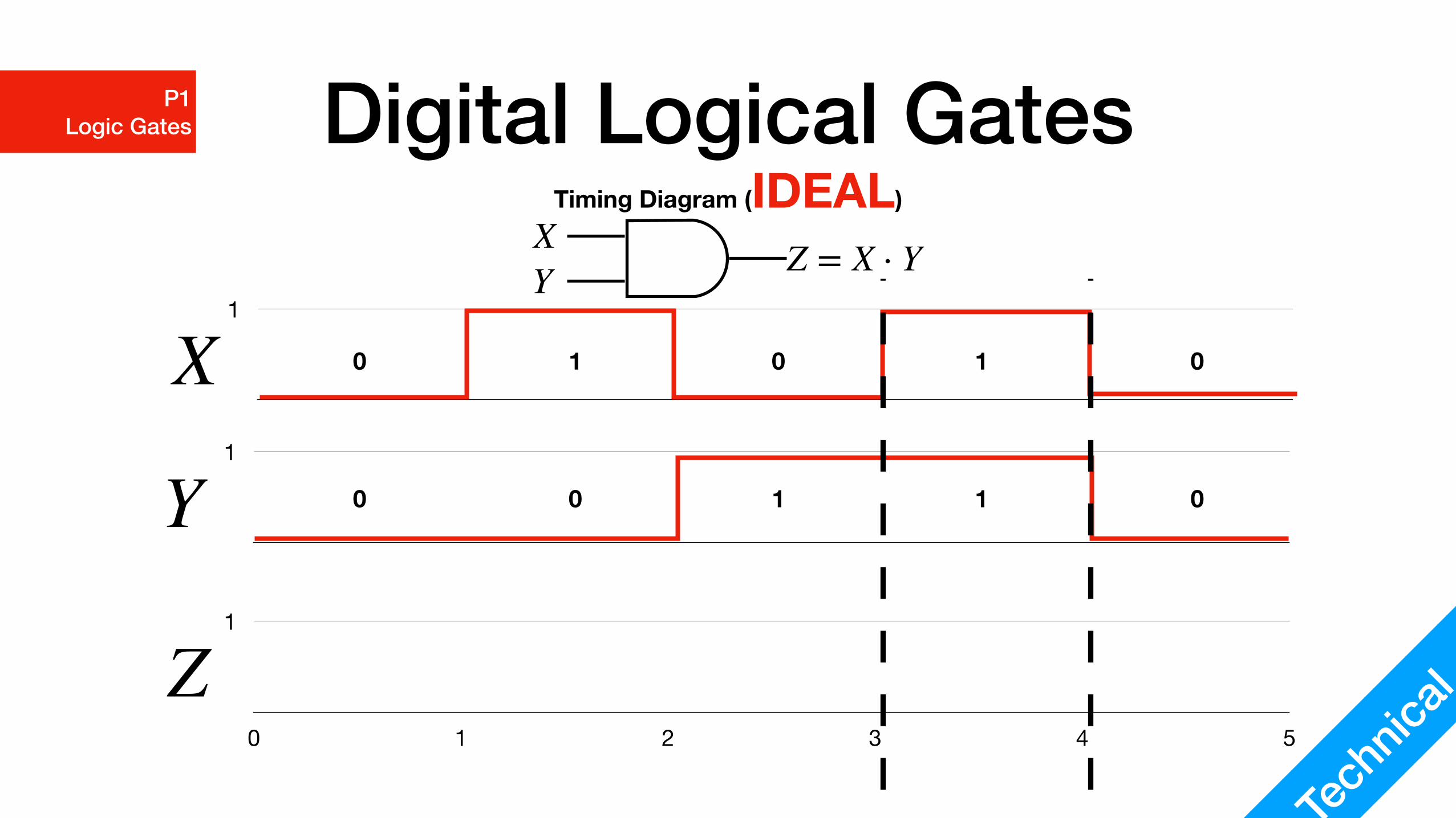
Digital Logical Gates
Tech
nical
P1 Logic Gates
Timing Diagram (IDEAL)
Z = X ⋅ YXY
1
X1
Y1
0 1 2 3 4 5
Z
0 1 0 1 0
0 0 1 1 0

Digital Logical Gates
Tech
nical
P1 Logic Gates
Timing Diagram (IDEAL)
Z = X ⋅ YXY
1
X1
Y1
0 1 2 3 4 5
Z
0 1 0 1 0
0 0 1 1 0
1

Digital Logical Gates
Tech
nical
P1 Logic Gates
Timing Diagram (REALITY)
Z = X ⋅ YXY
1
X1
Y1
0 1 2 3 4 5
Z
0 1 0 1 0
0 0 1 1 0

Digital Logical Gates
Tech
nical
P1 Logic Gates
Timing Diagram (REALITY)
Z = X ⋅ YXY
1
X1
Y1
0 1 2 3 4 5
Z
0 1 0 1 0
0 0 1 1 0
1
Digital Logical Gates
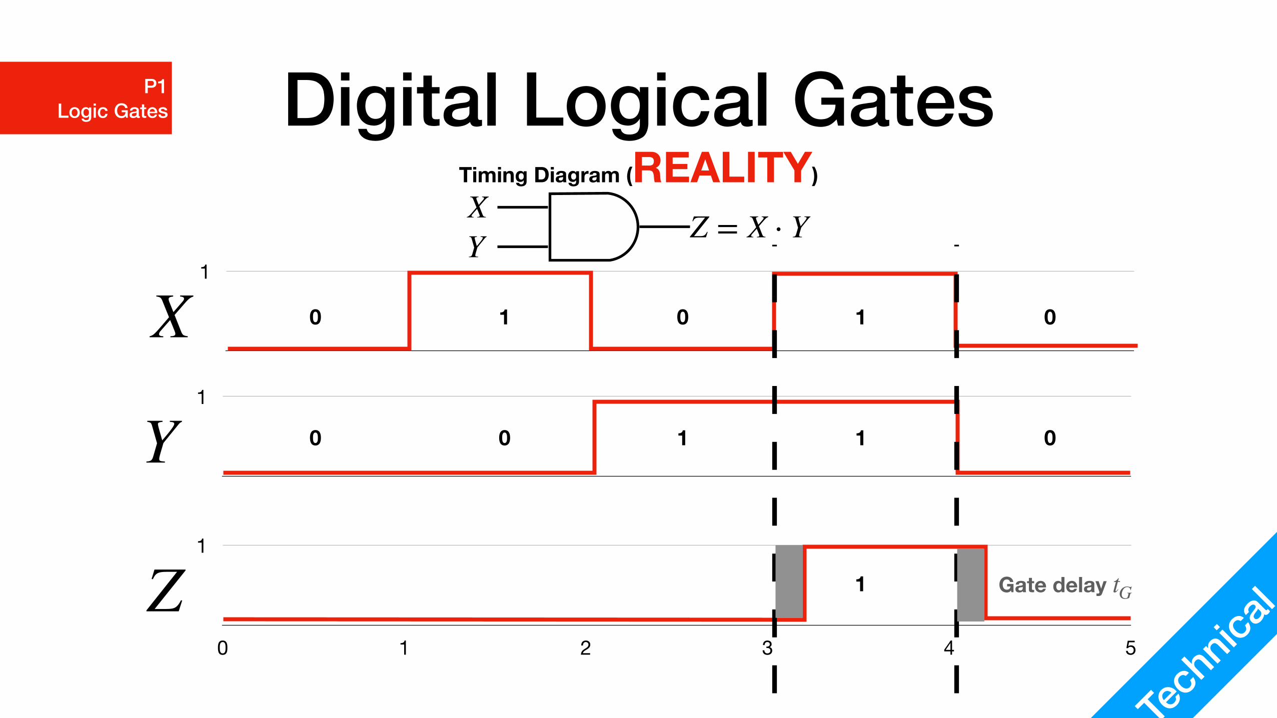
Tech
nical
P1 Logic Gates
Timing Diagram (REALITY)
Z = X ⋅ YXY
1
X1
Y1
0 1 2 3 4 5
Z
0 1 0 1 0
0 0 1 1 0
1 Gate delay tG

Gate Delay
Tech
nical
P1 Logic Gates
• Gate delay are small, but not ignorable in practice
• for simulation, you can ignore it for now
• Gate delay differs for different types and implementations of Gates
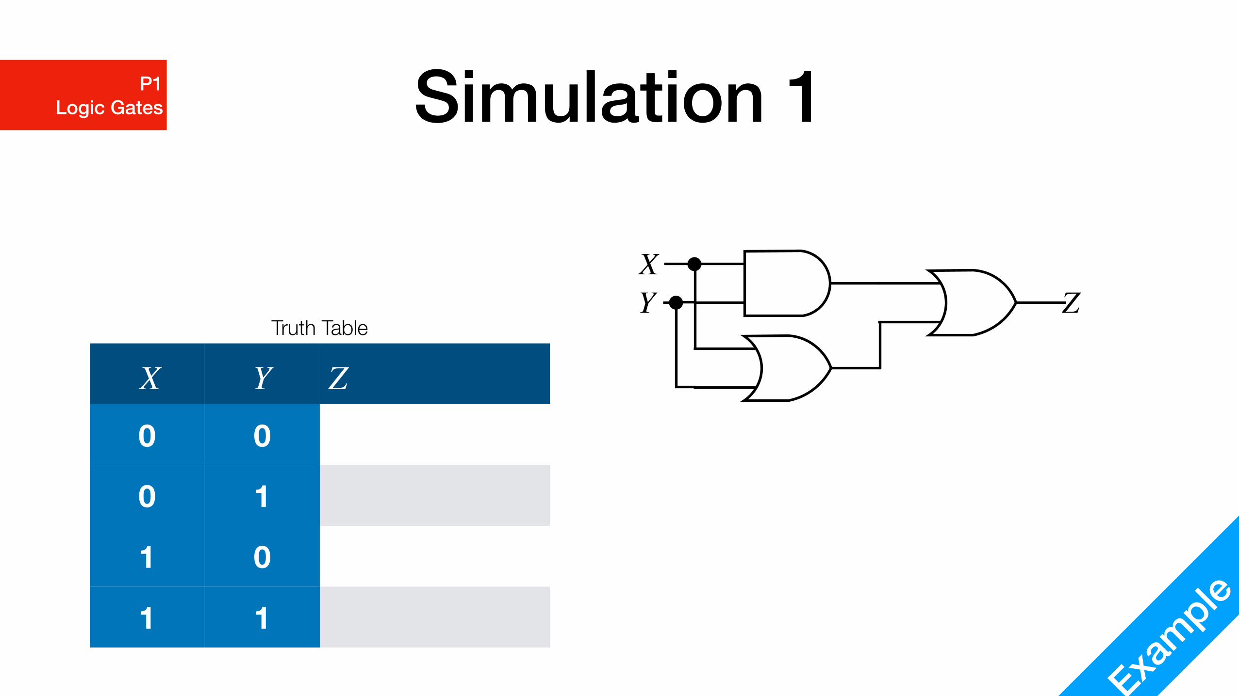
Simulation 1
Example
P1 Logic Gates
Truth Table
0 0
0 1
1 0
1 1
XY Z
ZYX

Simulation 1
Example
P1 Logic Gates
Truth Table
0 0
0 1
1 0
1 1
XY Z
ZYX = (X ⋅ Y) + (X + Y)

Simulation 2
Example
P1 Logic Gates
Truth Table
0 0 00 0 10 1 00 1 11 0 01 0 11 1 01 1 1
Z
YF
X
FYX Z

Simulation 2
Example
P1 Logic Gates
Truth Table
0 0 00 0 10 1 00 1 11 0 01 0 11 1 01 1 1
Z
YF
X
FYX = (XY) + (XZ)Z

Simulation 3
Example
P1 Logic Gates
Truth Table
0 0 00 0 10 1 00 1 11 0 01 0 11 1 01 1 1
Z
Y
F
X
FYX Z
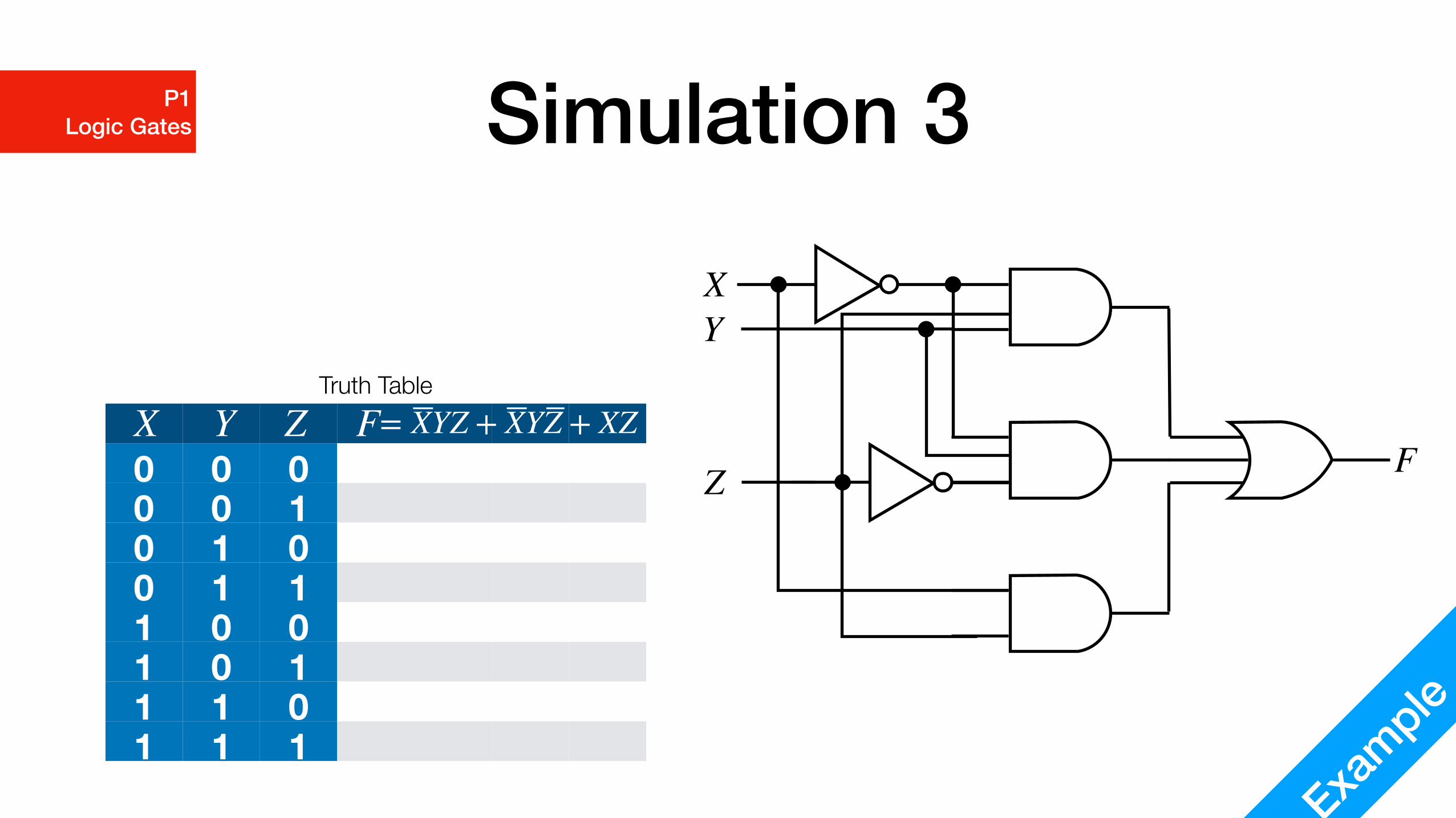
Simulation 3
Example
P1 Logic Gates
Truth Table
0 0 00 0 10 1 00 1 11 0 01 0 11 1 01 1 1
Z
Y
F
X
FYX = XYZ + XYZ + XZZ

Summary
• AND, OR, NOT Operators
• Logic Gates
• Timing diagram
• Truth Table
• Gate Delay
Review
P1 Logic Gates

LogicWorks
Summary
P2 Tutorial
Fire up your computer please!

Demo
P2 Tutorial
1. Open LogicWorks, Create new circuit diagram

Tech
nical
P2 Tutorial
1. This is the main interface

Tech
nical
P2 Tutorial
1. Select Simulation IO from the Parts Palette

Tech
nical
P2 Tutorial
1. Pay Attention to Binary Probe and Binary Switch

Tech
nical
P2 Tutorial
1. Double click and place one of each on the main board

Tech
nical
P2 Tutorial
1. Use the 'Draw Signal' tool to connect the two parts

Tech
nical
P2 Tutorial
1. Switch back to the Cursor mode, now click on the switch and you can change the signal value

Tech
nical
P2 Tutorial
1. Select Simulation Gates

Tech
nical
P2 Tutorial
1. Select AND-2, then complete the above diagram

Tech
nical
P2 Tutorial
1. Select Clock from Simulation IO, then replace the lower Binary Switch with it. A Clock is a device that generates a 1 at a certain frequency
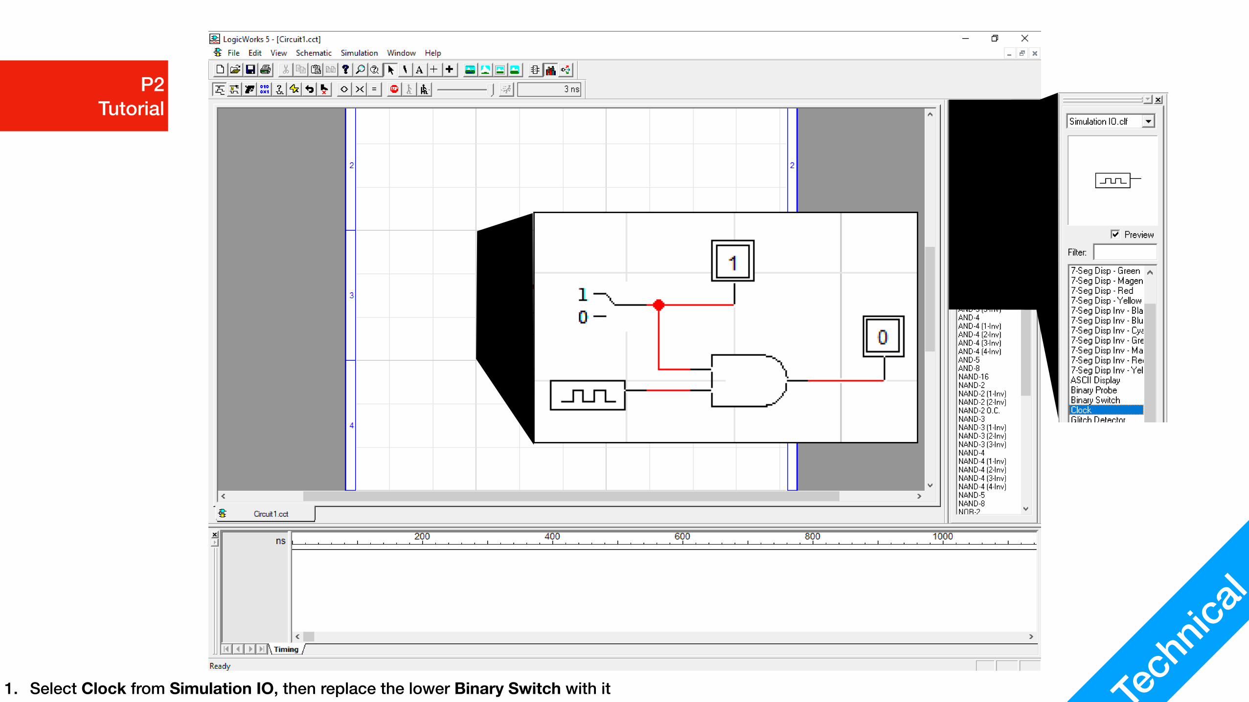
Tech
nical
P2 Tutorial
1. Select Clock from Simulation IO, then replace the lower Binary Switch with it

Tech
nical
P2 Tutorial
1. Right click the Red Wire, select Name

Tech
nical
P2 Tutorial
1. Complete the diagram like above, then click Reset Simulation
Tech
nical
P2 Tutorial
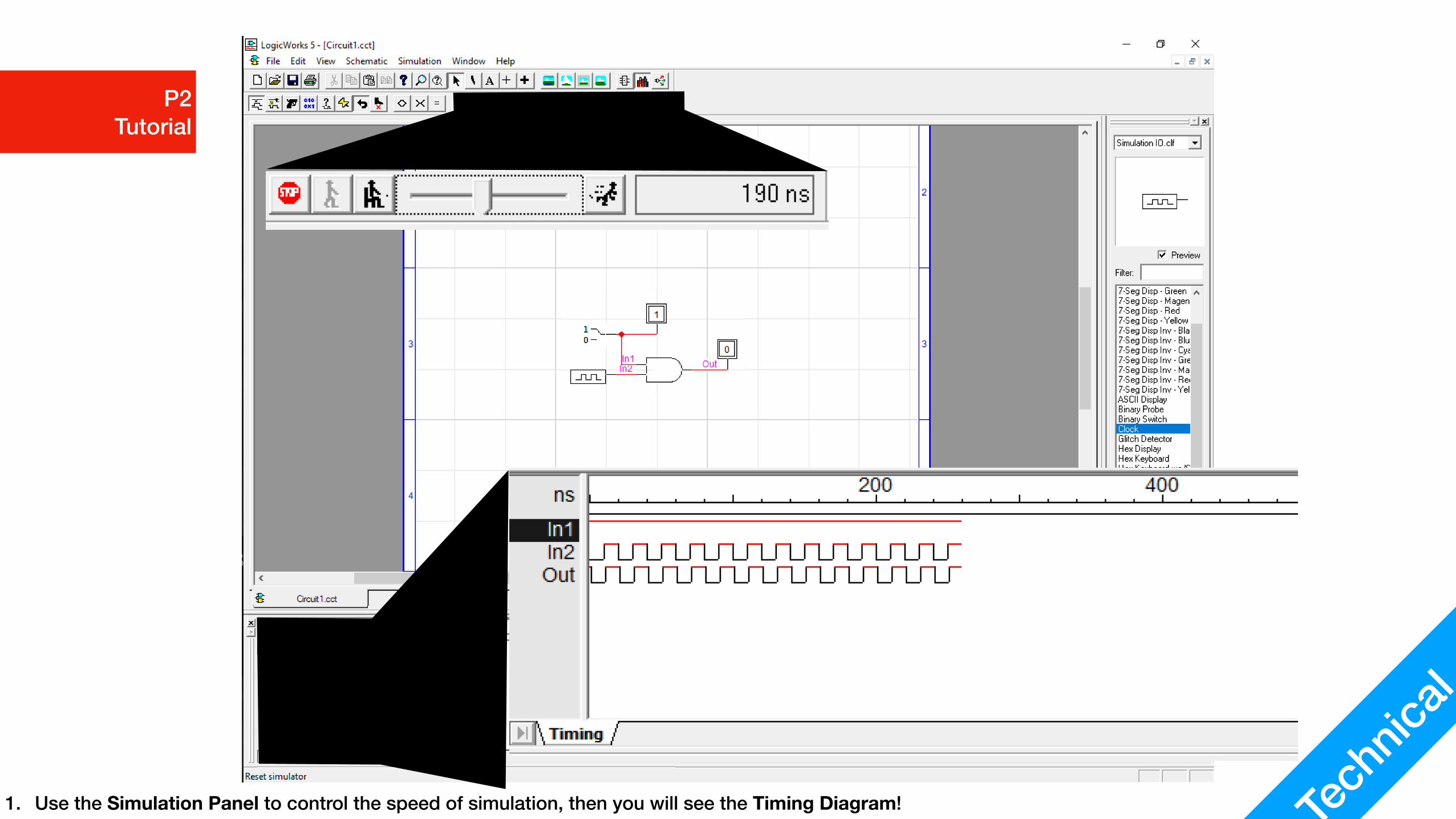
1. Use the Simulation Panel to control the speed of simulation, then you will see the Timing Diagram!

Exe 1• Curtain Motor Control
• Button1: 1 when user wants to open the curtain
• Button2: 1 when user wants to close the curtain
• Output1: 1 to make the motor open the curtain
• Output2: 1 to make the motor close the curtain
• Light: motor is active
Exerci
se
P2 Tutorial
• When both buttons are pressed, motors do nothing

Exe 2• Curtain Motor Control
• Sensor1: 1 when curtain is fully closed
• Sensor2: 1 when curtain is fully open
• Button1: 1 when user wants to open the curtain
• Button2: 1 when user wants to close the curtain
• Output1: 1 to make the motor open the curtain
• Output2: 1 to make the motor close the curtain
• Light: motor is active
Exerci
se
P2 Tutorial
• Stop the motor when the curtain is already fully opened/closed
Summary
• Simulation in LogicWorks
• Binary Probe / Binary Switch in LogicWorks
• Gates in LogicWorks
• Clocks in LogicWorks
• Timing Diagram in LogicWorks
Review
P2 Tutorial