· (typ) discharge path is connected between output and ground to provide rapid discharge of the...
TRANSCRIPT

austriamicrosystems AG
is now
ams AG The technical content of this austriamicrosystems datasheet is still valid.
Contact information:
Headquarters:
ams AG
Tobelbaderstrasse 30
8141 Unterpremstaetten, Austria
Tel: +43 (0) 3136 500 0
e-Mail: [email protected]
Please visit our website at www.ams.com
AS1376 1A, Low Input Vo l tage, Low Quiescent Current LDO
Datasheet
lid
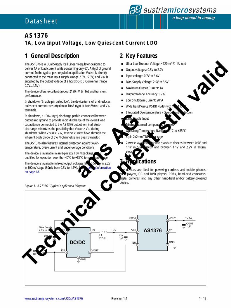
1 General DescriptionThe AS1376 is a Dual Supply Rail Linear Regulator designed to deliver 1A of load current while consuming only 67µA (typ) of ground current. In the typical post regulation application VBIAS is directly connected to the main input supply, (range 2.5V...5.5V) and VIN is supplied by the output voltage of a host DC-DC Converter (range 0.7V...4.5V).The device offers excellent dropout (120mV @ 1A) and transient performance.
In shutdown (Enable pin pulled low), the device turns off and reduces quiescent current consumption to 10nA (typ) at both VBIAS and VIN terminals.
In shutdown, a 100 (typ) discharge path is connected between output and ground to provide rapid discharge of the overall load capacitance connected to the AS1376 output terminal. Auto-discharge minimizes the possibility that VOUT > VIN during shutdown. When VOUT > VIN, reverse current flows through the inherent body diode of the N-channel series pass transistor.
The AS1376 also features internal protection against over-temperature, over-current and under-voltage conditions.
The device is available in an 8-pin 2x2 TDFN package and is qualified for operation over the -40ºC to +85ºC temperature range.
The device is available in fixed output voltages from 0.5V up to 2.2V in 100mV steps (50mV from 0.5V to 1.1V). See Ordering Information on page 18.
Figure 1. AS1376 - Typical Application Diagram
2 Key FeaturesUltra-Low Dropout Voltage: <120mV @ 1A load
Output voltages: 0.5V to 2.2V
Input voltage: 0.7V to 3.6V
Bias Supply Voltage: 2.5V to 5.5V
Maximum Output Current: 1A
Output Voltage Accuracy: ±2%
Low Shutdown Current: 20nA
Wide band VBIAS PSRR 45dB (typ) 10mA load
Integrated Overtemperature / Overcurrent Protection
Chip Enable Input
Minimal external components required
Operating Temperature Range: -40°C to +85°C
8-pin 2x2mm TDFN Package
2 weeks availability for non-standard devices between 0.5V and 1.1V in 50mV steps and between 1.1V and 2.2V in 100mV steps.
3 ApplicationsThe devices are ideal for powering cordless and mobile phones, MP3 players, CD and DVD players, PDAs, hand-held computers, digital cameras and any other hand-held and/or battery-powered device.
ams A
G
Technica
l conten
t still
va
www.austriamicrosystems.com/LODs/AS1376 Revision 1.4 1 - 19
AS1376Datasheet - P i n A s s i g n m e n t s
lid
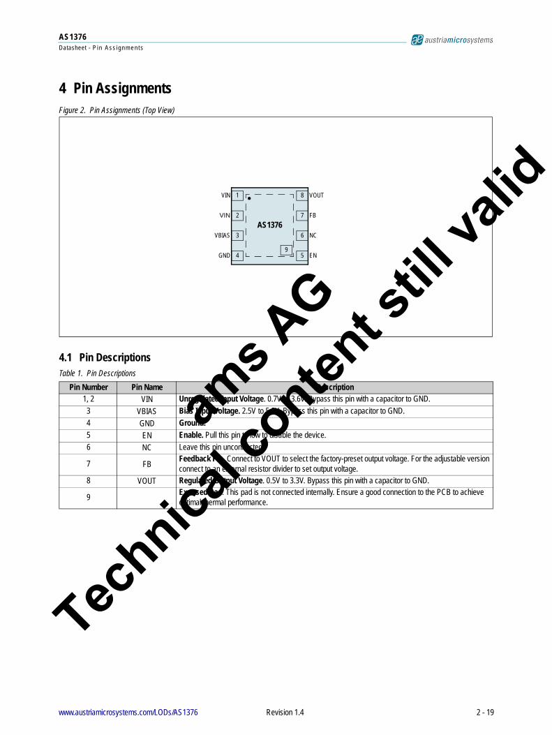
4 Pin AssignmentsFigure 2. Pin Assignments (Top View)
4.1 Pin DescriptionsTable 1. Pin Descriptions
Pin Number Pin Name Description1, 2 VIN Unregulated Input Voltage. 0.7V to 3.6V. Bypass this pin with a capacitor to GND.
3 VBIAS Bias Input Voltage. 2.5V to 5.5V. Bypass this pin with a capacitor to GND.
4 GND Ground.
5 EN Enable. Pull this pin to low to disable the device.
6 NC Leave this pin unconnected.
7 FBFeedback Pin. Connect to VOUT to select the factory-preset output voltage. For the adjustable version connect to an external resistor divider to set output voltage.
8 VOUT Regulated Output Voltage. 0.5V to 3.3V. Bypass this pin with a capacitor to GND.
9Exposed Pad. This pad is not connected internally. Ensure a good connection to the PCB to achieve optimal thermal performance.
5 EN
3VBIAS
2VIN
1VIN 8 VOUT
AS1376
4GND
7 FB
6 NC
9
ams A
G
Technica
l conten
t still
va
www.austriamicrosystems.com/LODs/AS1376 Revision 1.4 2 - 19

AS1376Datasheet - A b s o l u t e M a x i m u m R a t i n g s
lid
5 Absolute Maximum RatingsStresses beyond those listed in Table 2 may cause permanent damage to the device. These are stress ratings only and functional operation of the device at these or any other conditions beyond those indicated in Section 6 Electrical Characteristics on page 4 is not implied. Exposure to absolute maximum rating conditions for extended periods may affect device reliability.
Table 2. Absolute Maximum Ratings
Parameter Min Max Units Notes
Electrical Parameters
VIN to GND -0.3 5 V
VBIAS, EN to GND -0.3 +6.5 V
VOUT to GND -0.3 VIN + 0.3 V
Output Short-Circuit Duration Indefinite
Input Current (latch-up immunity) -100 100 mA JEDEC 78
Electrostatic Discharge
Electrostatic Discharge HBM 2 kV Norm: MIL 883 E method 3015
Temperature Ranges and Storage Conditions
Thermal Resistance JA 97 ºC/W
Junction-to-ambient thermal resistance is very dependent on application and board-layout. In
situations where high maximum power dissipation exists, special attention must be paid
to thermal dissipation during board design.
Junction Temperature +125 ºC
Storage Temperature Range -55 +150 ºC
Humidity non-condensing 5 85 %
Package Body Temperature +260 ºC
The reflow peak soldering temperature (body temperature) specified is in accordance with IPC/JEDEC J-STD-020 “Moisture/Reflow Sensitivity
Classification for Non-Hermetic Solid State Surface Mount Devices”.
The lead finish for Pb-free leaded packages is matte tin (100% Sn).
Humidity non-condensing 5 85 %
ams A
G
Technica
l conten
t still
va
www.austriamicrosystems.com/LODs/AS1376 Revision 1.4 3 - 19

AS1376Datasheet - E l e c t r i c a l C h a r a c t e r i s t i c s
lid
6 Electrical CharacteristicsVIN = VOUT + 0.2V, VBIAS = VOUT + 1.5V (or 2.5V whichever is larger), EN = VBIAS, CIN = COUT = 1µF, CBIAS = 4.7µF, TAMB = -40ºC to +85ºC. Typical values are at TAMB = +25ºC (unless otherwise specified).
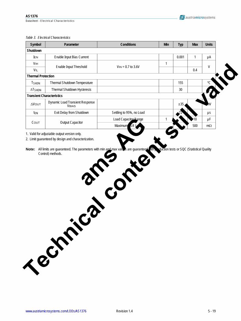
Table 3. Electrical Characteristics
Symbol Parameter Conditions Min Typ Max Units
TAMB Operating Temperature Range -40 +85 °C
VIN Input Voltage 0.7 3.6 V
VBIAS Bias Supply Voltage 2.5 5.5 V
VOUT Output Voltage Available in 100mV steps(see Ordering Information on page 18) 0.5 3.3 V
VOUT(NOM) - VOUT
Output Voltage AccuracyIOUT = 100µA -1.5 +1.5
% IOUT = 0A to 1A -2 +2
VFB Feedback Voltage1
IOUT = 100µA 492 500 508mV
IOUT = 0A to 1A 490 500 510
VOUT / VIN
Line Regulation VIN IOUT = 100µA 40 µV/V
VOUT /VBIAS
Line Regulation VBIAS IOUT = 100µA 135 µV/V
VLDR Load Regulation IOUT = 1mA to 1A 0.0002 %/mA
IOUT Output Current2 1 A
ILIM Current Limit VOUT forced to 90% of nominal VOUT 1.35 A
VDROP -VIN Output Voltage Dropout VIN
VBIAS = VOUT + 1.5V, IOUT = 1A 120mV
VBIAS = VOUT + 1.8V, IOUT = 1A 115
VBIAS = VOUT + 2.1V, IOUT = 1A 110mV
VBIAS = 5.5V, IOUT = 1A 105
VDROP -VBIAS
Output Voltage Dropout VBIASIOUT = 500mA 0.85
VIOUT = 1A 1.1
En Output Voltage Noise f = 10Hz to 100kHz, IOUT = 1mA 65 µVRMS
PSRR - VIN Power-Supply Rejection Ratio
Sine modulated VIN
f = 100Hz, IOUT = 10mA 78
dB f = 1kHz, IOUT = 10mA 61
f = 10kHz, IOUT = 10mA 54
f = 100kHz, IOUT = 10mA 60
PSRR - VBIAS
Power-Supply Rejection RatioSine modulated VBIAS
f = 100Hz, IOUT = 10mA 69
dBf = 1kHz, IOUT = 10mA 51
f = 10kHz, IOUT = 10mA 45
f = 100kHz, IOUT = 10mA 45
IQ_VBIAS Quiescent Current into VBIAS 60 120µA
IQ_VIN Quiescent Current into VIN IOUT = 0mA 6.5 8
ISHDN -VBIAS
Shutdown Current into VBIAS
VEN = 0V
0.02
µAISHDN -
VINShutdown Current into VIN 0.02
ams A
G
Technica
l conten
t still
va
www.austriamicrosystems.com/LODs/AS1376 Revision 1.4 4 - 19
AS1376Datasheet - E l e c t r i c a l C h a r a c t e r i s t i c s
lid
Note: All limits are guaranteed. The parameters with min and max values are guaranteed with production tests or SQC (Statistical Quality Control) methods.
Shutdown
IEN Enable Input Bias Current 0.001 1 µA
VIHEnable Input Threshold VIN = 0.7 to 3.6V
1V
VIL 0.4
Thermal Protection
TSHDN Thermal Shutdown Temperature 155 ºC
TSHDN Thermal Shutdown Hysteresis 30 ºC
Transient Characteristics
VOUTDynamic Load Transient Response
VBIAS ±35 mV
tON Exit Delay from Shutdown Settling to 95%, no Load 72 µs
COUT Output CapacitorLoad Capacitor Range 1 10 µF
Maximum ESR Load 500 m
1. Valid for adjustable output version only.
2. Limit guaranteed by design and characterization.
Table 3. Electrical Characteristics
Symbol Parameter Conditions Min Typ Max Units
ams A
G
Technica
l conten
t still
va
www.austriamicrosystems.com/LODs/AS1376 Revision 1.4 5 - 19

AS1376Datasheet - Ty p i c a l O p e r a t i n g C h a r a c t e r i s t i c s
7 Typical Operating CharacteristicsVIN = 1.2V, VBIAS = 2.5V, VOUT = 1.0V, EN = VBIAS, CIN = COUT = 1µF, CBIAS = 4µF. Typical values are at TAMB = +25ºC (unless otherwise specified).
lid
Figure 3. Bias Supply Current vs. Bias Supply Voltage Figure 4. Bias Supply Current vs. Bias Supply Voltage50
55
60
65
70
2.5 3 3.5 4 4.5 5 5.5Bias Supply Voltage (V)
Bia
s S
up
ply
Cu
rre
nt (
µA
)
no loadIout = 700mAIout = 1A
40
45
50
55
60
65
70
75
80
2.5 3 3.5 4 4.5 5 5.5Bias Supply Voltage (V)
Bia
s S
up
ply
Cu
rre
nt (
µA
)
- 40°C
+ 25°C
+ 90°C
G still v
a
Figure 5. Ground Current vs. Bias Supply Voltage Figure 6. Ground Current vs. Bias Supply Voltage
50
55
60
65
70
75
80
85
90
2.5 3 3.5 4 4.5 5 5.5Bias Supply Voltage (V)
Gro
un
d C
urr
en
t (µ
A)
- 40°C
+ 25°C
+ 90°C
no load
50
55
60
65
70
75
80
85
90
95
2.5 3 3.5 4 4.5 5 5.5Bias Supply Voltage (V)
Gro
un
d C
urr
en
t (µ
A)
- 40°C
+ 25°C
+ 90°C
Iout=1A
ams A
al co
ntent
Figure 7. Ground Current vs. Bias Supply Voltage Figure 8. Ground Current vs. Load Current
60
65
70
75
80
2.5 3 3.5 4 4.5 5 5.5Bias Supply Voltage (V)
Gro
un
d C
urr
en
t (µ
A)
no load
Iout = 1A 50
55
60
65
70
75
80
85
0 100 200 300 400 500 600 700 800 900 1000
Load Current (mA)
Gro
un
d C
urr
en
t (µ
A)
-40°C
+25°C
+90°CTechnic
www.austriamicrosystems.com/LODs/AS1376 Revision 1.4 6 - 19

AS1376Datasheet - Ty p i c a l O p e r a t i n g C h a r a c t e r i s t i c s
lid
Figure 9. PSRR VIN ; VIN=1.5VDC + 300mVpk Figure 10. PSRR VBIAS; VBIAS=3.5VDC + 500mVpk
-100
-90
-80
-70
-60
-50
-40
100 1000 10000 100000Frequency (Hz)
Inp
ut V
olta
ge
- P
SR
R (
dB
)
-100
-90
-80
-70
-60
-50
-40
100 1000 10000 100000Frequency (Hz)
Bia
s S
up
ply
Vo
ltag
e -
PS
RR
(d
B) Iout=10mA
ill va
Figure 11. Line Regulation: VOUT vs. VIN; IOUT=100µA Figure 12. Line Regulation: VOUT vs. VIN; VBIAS=5.5V
0.985
0.99
0.995
1
1.005
1.01
1.015
1.2 1.4 1.6 1.8 2 2.2 2.4 2.6 2.8 3 3.2 3.4 3.6
Input Voltage (V)
Ou
tpu
t Vo
ltag
e (
V)
0.985
0.99
0.995
1
1.005
1.01
1.015
1.2 1.4 1.6 1.8 2 2.2 2.4 2.6 2.8 3 3.2 3.4 3.6
Input Voltage (V)
Ou
tpu
t Vo
ltag
e (
V)
ams A
G
al co
ntent s
t
Figure 13. Load Regulation: VOUT vs. IOUT Figure 14. Output Voltage vs. Temperature; IOUT=1mA
0.985
0.99
0.995
1
1.005
1.01
1.015
0 200 400 600 800 1000Output Current (mA)
Ou
tpu
t Vo
ltag
e (
V)
0.985
0.99
0.995
1
1.005
1.01
1.015
-40 -20 0 20 40 60 80Temperature (°C)
Ou
tpu
t Vo
ltag
e (
V)
Technic
www.austriamicrosystems.com/LODs/AS1376 Revision 1.4 7 - 19

AS1376Datasheet - Ty p i c a l O p e r a t i n g C h a r a c t e r i s t i c s
lid
Figure 15. Dropout VIN vs. Temperature; IOUT=1A Figure 16. Enable Start-up
50
75
100
125
150
175
200
-40 -20 0 20 40 60 80Temperature (°C)
Dro
po
ut V
IN (
mV
)
50µs/Div
500m
V/D
iv
500m
V/D
iv
ENVO
UT
ill va
ams A
G
al co
ntent s
t
Technic
www.austriamicrosystems.com/LODs/AS1376 Revision 1.4 8 - 19

AS1376Datasheet - D e t a i l e d D e s c r i p t i o n
lid
8 Detailed DescriptionThe AS1376 is a low-dropout, low-quiescent-current linear regulator intended for LDO regulator applications where output current load requirements range from no load to 1A. All devices come with fixed output voltage from 0.5V to 3.3V. (see Ordering Information on page 18).
Shutdown current for the whole regulator is typically 20nA. The device has integrated short-circuit and over current protection. Under-Voltage lockout prevents erratic operation when the input voltage is slowly decaying (e.g. in a battery powered application). Thermal Protection shuts down the device when die temperature reaches 150°C. This is a useful protection when the device is under sustained short circuit conditions.
As illustrated in Figure 17, the devices comprise voltage reference, error amplifier, N-channel MOSFET pass transistor, internal voltage divider, current limiter, thermal sensor and shutdown logic.
The bandgap reference is connected to the inverting input of the error amplifier. The error amplifier compares this reference with the feedback voltage and amplifies the difference. If the feedback voltage is lower than the reference voltage, the N-channel MOSFET gate is pulled higher, allowing more current to pass to the output, and increases the output voltage. If the feedback voltage is too high, the pass-transistor gate is pulled down, allowing less current to pass to the output.
When the adjustable output variant is selected, an external resistor voltage divider is connected to FB pin and a sample of the output is compared to the 500mV reference.
When a fixed output variant is chosen, FB must be connected to the Output pin. Depending upon the variant chosen, the internal reference is trimmed to the final output voltage. See Electrical Characteristics (page 4) for final voltages and tolerances.
Figure 17. AS1376 Block Diagram
RDISCHARGE
ShutdownPower On
Control Logic
ReferenceCore
Thermal Overload Protection
BandgapVoltage & Current
Reference
+
-Error
Amplifier
QDISCHARGE
OUT
VBIAS
VIN
GND
QPOWER
AS1376
EN
EP
FB
VIN
ams A
G
Technica
l conten
t still
va
www.austriamicrosystems.com/LODs/AS1376 Revision 1.4 9 - 19

AS1376Datasheet - D e t a i l e d D e s c r i p t i o n
lid
8.1 Output VoltagesStandard products are factory-set with output voltages from 0.5V to 2.2V. A two-digit suffix of the part number identifies the nominal output (see Ordering Information on page 18). Non-standard devices are available.
For more information contact: http://www.austriamicrosystems.com/contact
8.2 Advantages of Dual Supply Architecture vs Traditional Single Supply ApproachCompared to the traditional single supply approach, employing a P-channel series pass MOSFET, the dual rail architecture ensures improved performances in a LDO when operating at very low input voltages below the threshold of the internal series power N-channel MOSFET. The extra supply voltage at VBIAS (VBIAS > VIN) ensures that the N-channel MOSFET always operates above its threshold voltage.
Figure 18 shows simplified block diagrams of single supply P-channel LDO and dual rail N-channel series pass architectures.
Figure 18. Single vs. Dual Supply
The P-channel LDO uses a PMOS output transistor connected in a common source configuration. During regulation, the P-channel gate-source voltage moves between VIN and GND as the load demands. The dual supply approach is based on an N-channel output transistor in common drain configuration where the source is connected to the regulated output. During regulation, the N-channel gate source voltage increases from VOUT to VBIAS as the load demands. As the drain voltage is not shared with the remaining blocks of the circuit, its value can be chosen independently. The N-channel source follower design allows improved efficiency and dropout at low input voltages and provides faster load transient response.
Bandgap
erroramplifier
PMOS +
-
coreblocks
VIN
Bandgap
erroramplifier
NMOS +
-core
blocks
VINVBIAS
VOUTVOUT
Single SupplyDual Supply
ams A
G
Technica
l conten
t still
va
www.austriamicrosystems.com/LODs/AS1376 Revision 1.4 10 - 19

AS1376Datasheet - A p p l i c a t i o n I n f o r m a t i o n
lid
9 Application Information
9.1 Dropout VoltageDropout is the input to output voltage difference, below which the linear regulator ceases to regulate. At this point, the output voltage change follows the input voltage change. Dropout voltage may be measured at different currents and, in particular at the regulator maximum one. From this is obtained the MOSFET maximum series resistance over temperature etc. More generally:
(EQ 1)
Dropout is probably the most important specification when the regulator is used in a battery application. The dropout performance of the regulator defines the useful “end of life” of the battery before replacement or re-charge is required.
Figure 19. Graphical Representation of Dropout Voltage
Figure 19 shows the variation of VOUT as VIN is varied for a certain load current. The practical value of dropout is the differential voltage (VOUT-VIN) measured at the point where the LDO output voltage has fallen by 100mV below the nominal, fully regulated output value. The nominal regulated output voltage of the LDO is that obtained when there is 500mV (or greater) input-output voltage differential.
9.2 Auto-DischargeAS1376 features an auto-discharge function that discharges the load capacitance through a 100 (typ) path to ground when the device is placed in shutdown. This helps to minimizes the possibility that VOUT > VIN during shutdown caused by differing capacitance discharge rates at VIN and VOUT terminals.
When VOUT > VIN, reverse current flows through the inherent body diode of the N-channel series pass transistor. This current should be limited to 50mA or less. If this is not possible, then an external Schottky diode should be connected between VOUT (anode) and VIN (cathode) to bypass the discharge current around the AS1376.
9.3 EfficiencyLow quiescent current and low input-output voltage differential are important in battery applications amongst others, as the regulator efficiency is directly related to quiescent current and dropout voltage. Efficiency is given by:
Efficiency = % (EQ 2)
Where: IQ = Quiescent current of LDO measured at VBIAS
VDROPOUT ILOAD RSERIES=
DropoutVoltage
100mVVIN
VOUT
VOUT
VIN
VOUT
VIN = VOUT(TYP) + 0.5V
VIN
VLOAD ILOADVIN IQ ILOAD+ --------------------------------------- 100
ams A
G
Technica
l conten
t still
va
www.austriamicrosystems.com/LODs/AS1376 Revision 1.4 11 - 19
AS1376Datasheet - A p p l i c a t i o n I n f o r m a t i o n
lid
9.4 Power DissipationMaximum power dissipation (PD) of the LDO is the sum of the power dissipated by the internal series MOSFET and the quiescent current required to bias the internal voltage reference and the internal error amplifier, and is calculated as:
Watts (EQ 3)
Internal power dissipation as a result of the bias current for the internal voltage reference and the error amplifier is calculated as:
Watts (EQ 4)
Total LDO power dissipation is calculated as:
Watts (EQ 5)
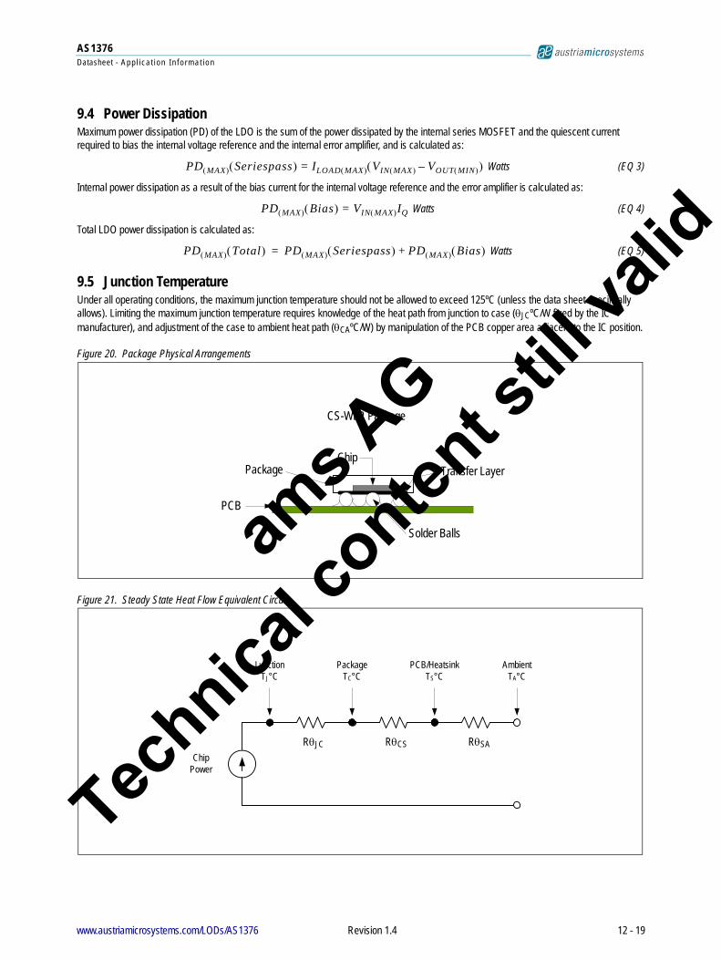
9.5 Junction TemperatureUnder all operating conditions, the maximum junction temperature should not be allowed to exceed 125ºC (unless the data sheet specifically allows). Limiting the maximum junction temperature requires knowledge of the heat path from junction to case (JCºC/W fixed by the IC manufacturer), and adjustment of the case to ambient heat path (CAºC/W) by manipulation of the PCB copper area adjacent to the IC position.
Figure 20. Package Physical Arrangements
Figure 21. Steady State Heat Flow Equivalent Circuit
PD MAX Seriespass ILOAD MAX = VIN MAX VOUT MIN –
PD MAX Bias VIN MAX IQ=
PD MAX Total PD MAX Seriespass PD MAX + Bias =
Chip
PCB
Package Transfer Layer
CS-WLP Package
Solder Balls
JunctionTJ°C
PackageTC°C
PCB/HeatsinkTS°C
AmbientTA°C
ChipPower
RJC RCS RSA
ams A
G
Technica
l conten
t still
va
www.austriamicrosystems.com/LODs/AS1376 Revision 1.4 12 - 19
AS1376Datasheet - A p p l i c a t i o n I n f o r m a t i o n
lid
Total Thermal Path Resistance:
(EQ 6)
Junction Temperature (TJºC) is determined by:
ºC (EQ 7)
9.6 Explanation of Steady State Specifications
9.6.1 Line RegulationLine regulation is defined as the change in output voltage when the input (or line) voltage is changed by a known quantity. It is a measure of the regulator’s ability to maintain a constant output voltage when the input voltage changes. Line regulation is a measure of the DC open loop gain of the error amplifier. More generally:
Line Regulation = and is a pure number (EQ 8)
In practise, line regulation is referred to the regulator output voltage in terms of % / VOUT. This is particularly useful when the same regulator is available with numerous output voltage trim options.
Line Regulation = % / V (EQ 9)
9.6.2 Load RegulationLoad regulation is defined as the change of the output voltage when the load current is changed by a known quantity. It is a measure of the regulator’s ability to maintain a constant output voltage when the load changes. Load regulation is a measure of the DC closed loop output resistance of the regulator. More generally:
Load Regulation = and is units of ohms () (EQ 10)
In practise, load regulation is referred to the regulator output voltage in terms of % / mA. This is particularly useful when the same regulator is available with numerous output voltage trim options.
Load Regulation = % / mA (EQ 11)
9.6.3 Setting AccuracyAccuracy of the final output voltage is determined by the accuracy of the ratio of R1 and R2, the reference accuracy and the input offset voltage of the error amplifier. When the regulator is supplied pre-trimmed, the output voltage accuracy is fully defined in the output voltage specification.
When the regulator has a SET terminal, the output voltage may be adjusted externally. In this case, the tolerance of the external resistor network must be incorporated into the final accuracy calculation. Generally:
(EQ 12)
The reference tolerance is given both at 25ºC and over the full operating temperature range.
9.6.4 Total AccuracyAway from dropout, total steady state accuracy is the sum of setting accuracy, load regulation and line regulation. Generally:
Total % Accuracy = Setting % Accuracy + Load Regulation % + Line Regulation % (EQ 13)
RJA RJC RCS RSA+ +=
TJ PD MAX RJA TAMB+=
VOUT
VIN
----------------
VOUT
VIN
---------------- 100VOUT
------------
VOUT
IOUT
----------------
VOUT
IOUT
---------------- 100VOUT
----------------
VOUT VSET VSET = 1R1 R1R2 R2---------------------+
ams A
G
Technica
l conten
t still
va
www.austriamicrosystems.com/LODs/AS1376 Revision 1.4 13 - 19
AS1376Datasheet - A p p l i c a t i o n I n f o r m a t i o n
lid
9.7 Explanation of Dynamic Specifications
9.7.1 Power Supply Rejection Ratio (PSRR)Known also as Ripple Rejection, this specification measures the ability of the regulator to reject noise and ripple beyond DC. PSRR is a summation of the individual rejections of the error amplifier, reference and AC leakage through the series pass transistor. The specification, in the form of a typical attenuation plot with respect to frequency, shows up the gain bandwidth compromises forced upon the designer in low quiescent current conditions. Generally:
PSSR = dB using lower case to indicate AC values (EQ 14)
Power supply rejection ratio is fixed by the internal design of the regulator. Additional rejection must be provided externally.
9.7.2 Output Capacitor ESRThe series regulator is a negative feedback amplifier, and as such is conditionally stable. The ESR of the output capacitor is usually used to cancel one of the open loop poles of the error amplifier in order to produce a single pole response. Excessive ESR values may actually cause instability by excessive changes to the closed loop unity gain frequency crossover point. The range of ESR values for stability is usually shown either by a plot of stable ESR versus load current, or a limit statement in the datasheet.
Some ceramic capacitors exhibit large capacitance and ESR variations with temperature and DC bias. Z5U and Y5V capacitors may be required to ensure stability at temperatures below TAMB = -10ºC. With X7R or X5R capacitors, a 1µF capacitor should be sufficient at all operating temperatures.
Larger output capacitor values (10µF max) help to reduce noise and improve load transient-response, stability and power-supply rejection.
9.7.3 Input CapacitorIf the AS1376 is used stand alone, an input capacitor at VIN is required for stability. It is recommended that a 1.0µF capacitor be connected between the AS1376 power supply input pin VIN and ground (capacitance value may be increased without limit).
This capacitor must be located at a distance of not more than 1cm from the VIN pin and returned to a clean analog ground. Any good quality ceramic, tantalum, or film capacitor may be used at the input.
A capacitor at VBIAS is not required if the distance to the supply does not exceed 5cm.
If the AS1376 device is used in the typical application as post regulator after a DC-DC regulator, no input capacitors are required at all as the capacitors of the DC-DC regulator (CIN and COUT) are sufficient if both components are mounted close to each other and a proper GND plane is used. If the distance between the output capacitor of the DC-DC regulator and the VIN pin of the AS1376 is larger than 5cm, a capacitor at VIN is recommended.
9.7.4 NoiseThe regulator output is a DC voltage with noise superimposed on the output. The noise comes from three sources; the reference, the error amplifier input stage, and the output voltage setting resistors. Noise is a random fluctuation and if not minimized in some applications, will produce system problems.
9.7.5 Transient ResponseThe series regulator is a negative feedback system, and therefore any change at the output will take a finite time to be corrected by the error loop. This “propagation time” is related to the bandwidth of the error loop. The initial response to an output transient comes from the output capacitance, and during this time, ESR is the dominant mechanism causing voltage transients at the output. More generally:
Units are Volts, Amps, Ohms. (EQ 15)
Thus an initial +50mA change of output current will produce a -12mV transient when the ESR=240m. Remember to keep the ESR within stability recommendations when reducing ESR by adding multiple parallel output capacitors.
After the initial ESR transient, there follows a voltage droop during the time that the LDO feedback loop takes to respond to the output change. This drift is approx. linear in time and sums with the ESR contribution to make a total transient variation at the output of:
Units are Volts, Seconds, Farads, Ohms. (EQ 16)
Where:CLOAD is output capacitorT = Propagation delay of the LDO
20LogVOUT
VIN
----------------
VTRANSIENT IOUTPUT RESR=
VTRANSIENT IOUTPUT= RESRT
CLOAD
----------------+
ams A
G
Technica
l conten
t still
va
www.austriamicrosystems.com/LODs/AS1376 Revision 1.4 14 - 19

AS1376Datasheet
lid
This shows why it is convenient to increase the output capacitor value for a better support for fast load changes. Of course the formula holds for t < “propagation time”, so that a faster LDO needs a smaller cap at the load to achieve a similar transient response. For instance 50mA load current step produces 50mV output drop if the LDO response is 1usec and the load cap is 1µF.
There is also a steady state error caused by the finite output impedance of the regulator. This is derived from the load regulation specification discussed above.
9.7.6 Exit from Shutdown DelayThis specification defines the time taken for the LDO to awake from shutdown. The time is measured from the release of the enable pin to the time that the output voltage is within 5% of the final value. It assumes that the voltage at VIN is stable and within the regulator min and max limits. Shutdown reduces the quiescent current to very low, mostly leakage values (<1µA).
9.7.7 Thermal ProtectionTo prevent operation under extreme fault conditions, such as a permanent short circuit at the output, thermal protection is built into the device. Die temperature is measured, and when a 150ºC threshold is reached, the device enters shutdown. When the die cools sufficiently, the device will restart (assuming input voltage exists and the device is enabled). Hysteresis of 25ºC prevents low frequency oscillation between start-up and shutdown around the temperature threshold.
9.7.8 Power Supply SequencingThe AS1376 requires two different supply voltages active at the same time for correct operation. They are as given below.
1. VIN, the power input voltage, that is regulated to provide the fixed output voltage.
2. VBIAS, the bias input voltage, supplies internal circuitry.
It's important that VIN does not exceed VBIAS at any time. If the device is used in the typical post regulation application as shown in Figure 1, the sequencing of the two power supplies is not an issue as VBIAS supplies both, the DC-DC regulator and the AS1376. The output voltage of the DC-DC regulator will take some time to rise up and supply VIN of AS1376. In this application VIN will always ramp up more slowly than VBIAS. In case VIN is shorted to VBIAS, the voltages at the two supply pins will ramp up simultaneously causing no problem. Only in applications with two independent supplies connected to the AS1376 special care must be taken to guarantee that VIN is always = VBIAS.
9.7.9 Auto-DischargeWhen the AS1376 is placed in shutdown, a 100 path to ground is connected at the output. This path speeds up the discharge of the capacitor(s) connected to the regulator output. Assuming that VIN remains constant and always >VOUT, output discharge time is calculated from the following relationship:
(EQ 17)
Where:t = specified time after regulator shutdown (sec)VREG = Regulated output voltage (initial condition)R = 100 (typ) discharge resistanceC = Output capacitance (Farad)
In other words, the output discharge will reach 90% below the regulated output voltage in 2.2RC seconds; R and C defined as above.
V t VREGet
RC--------–
=am
s AG
Technica
l conten
t still
va
www.austriamicrosystems.com/LODs/AS1376 Revision 1.4 15 - 19
AS1376Datasheet - P a c k a g e D r a w i n g s a n d M a r k i n g s
lid
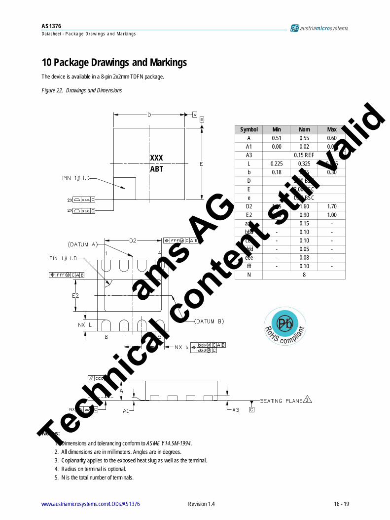
10 Package Drawings and MarkingsThe device is available in a 8-pin 2x2mm TDFN package.
Figure 22. Drawings and Dimensions
Notes:
1. Dimensions and tolerancing conform to ASME Y14.5M-1994.
2. All dimensions are in millimeters. Angles are in degrees.
3. Coplanarity applies to the exposed heat slug as well as the terminal.
4. Radius on terminal is optional.
5. N is the total number of terminals.
XXXABT
Symbol Min Nom Max
A 0.51 0.55 0.60
A1 0.00 0.02 0.05
A3 0.15 REF
L 0.225 0.325 0.425
b 0.18 0.25 0.30
D 2.00 BSC
E 2.00 BSC
e 0.50 BSC
D2 1.45 1.60 1.70
E2 0.75 0.90 1.00
aaa - 0.15 -
bbb - 0.10 -
ccc - 0.10 -
ddd - 0.05 -
eee - 0.08 -
fff - 0.10 -
N 8
ams A
G
Technica
l conten
t still
va
www.austriamicrosystems.com/LODs/AS1376 Revision 1.4 16 - 19

AS1376Datasheet - P a c k a g e D r a w i n g s a n d M a r k i n g s
lid
Revision History
Note: Typos may not be explicitly mentioned under revision history.
Revision Date Owner Description
1.2 Initial revision
1.3 12 Oct, 2011afe
Changes made across document for version 1.3
1.4 12 Dec, 2011 Updated equations in Power Dissipation section
ams A
G
Technica
l conten
t still
va
www.austriamicrosystems.com/LODs/AS1376 Revision 1.4 17 - 19
AS1376Datasheet - O r d e r i n g I n f o r m a t i o n
lid
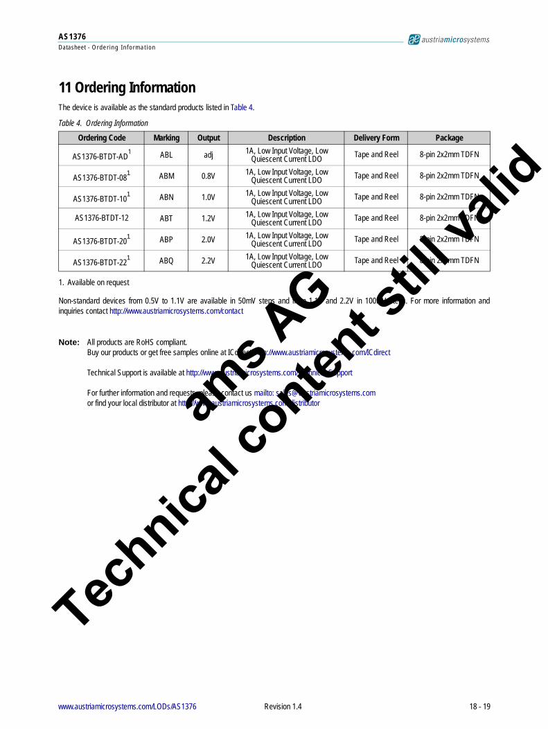
11 Ordering InformationThe device is available as the standard products listed in Table 4.
Non-standard devices from 0.5V to 1.1V are available in 50mV steps and from 1.1V and 2.2V in 100mV steps. For more information and inquiries contact http://www.austriamicrosystems.com/contact
Note: All products are RoHS compliant.Buy our products or get free samples online at ICdirect: http://www.austriamicrosystems.com/ICdirectTechnical Support is available at http://www.austriamicrosystems.com/Technical-SupportFor further information and requests, please contact us mailto: [email protected] find your local distributor at http://www.austriamicrosystems.com/distributor
Table 4. Ordering Information
Ordering Code Marking Output Description Delivery Form Package
AS1376-BTDT-AD1
1. Available on request
ABL adj 1A, Low Input Voltage, Low Quiescent Current LDO Tape and Reel 8-pin 2x2mm TDFN
AS1376-BTDT-081 ABM 0.8V 1A, Low Input Voltage, Low
Quiescent Current LDO Tape and Reel 8-pin 2x2mm TDFN
AS1376-BTDT-101 ABN 1.0V 1A, Low Input Voltage, Low
Quiescent Current LDO Tape and Reel 8-pin 2x2mm TDFN
AS1376-BTDT-12 ABT 1.2V 1A, Low Input Voltage, Low Quiescent Current LDO Tape and Reel 8-pin 2x2mm TDFN
AS1376-BTDT-201 ABP 2.0V 1A, Low Input Voltage, Low
Quiescent Current LDO Tape and Reel 8-pin 2x2mm TDFN
AS1376-BTDT-221 ABQ 2.2V 1A, Low Input Voltage, Low
Quiescent Current LDO Tape and Reel 8-pin 2x2mm TDFN
ams A
G
Technica
l conten
t still
va
www.austriamicrosystems.com/LODs/AS1376 Revision 1.4 18 - 19
AS1376Datasheet - O r d e r i n g I n f o r m a t i o n
lid
Copyrights
Copyright © 1997-2011, austriamicrosystems AG, Tobelbaderstrasse 30, 8141 Unterpremstaetten, Austria-Europe. Trademarks Registered ®. All rights reserved. The material herein may not be reproduced, adapted, merged, translated, stored, or used without the prior written consent of the copyright owner.
All products and companies mentioned are trademarks or registered trademarks of their respective companies.
Disclaimer
Devices sold by austriamicrosystems AG are covered by the warranty and patent indemnification provisions appearing in its Term of Sale. austriamicrosystems AG makes no warranty, express, statutory, implied, or by description regarding the information set forth herein or regarding the freedom of the described devices from patent infringement. austriamicrosystems AG reserves the right to change specifications and prices at any time and without notice. Therefore, prior to designing this product into a system, it is necessary to check with austriamicrosystems AG for current information. This product is intended for use in normal commercial applications. Applications requiring extended temperature range, unusual environmental requirements, or high reliability applications, such as military, medical life-support or life-sustaining equipment are specifically not recommended without additional processing by austriamicrosystems AG for each application. For shipments of less than 100 parts the manufacturing flow might show deviations from the standard production flow, such as test flow or test location.
The information furnished here by austriamicrosystems AG is believed to be correct and accurate. However, austriamicrosystems AG shall not be liable to recipient or any third party for any damages, including but not limited to personal injury, property damage, loss of profits, loss of use, interruption of business or indirect, special, incidental or consequential damages, of any kind, in connection with or arising out of the furnishing, performance or use of the technical data herein. No obligation or liability to recipient or any third party shall arise or flow out of austriamicrosystems AG rendering of technical or other services.
Contact Information
Headquarters
austriamicrosystems AGTobelbaderstrasse 30A-8141 Unterpremstaetten, Austria
Tel: +43 (0) 3136 500 0Fax: +43 (0) 3136 525 01
For Sales Offices, Distributors and Representatives, please visit:
http://www.austriamicrosystems.com/contact
ams A
G
Technica
l conten
t still
va
www.austriamicrosystems.com/LODs/AS1376 Revision 1.4 19 - 19