turn-off conditions for power scrsseagrant.mit.edu/publications/mitsg_13-50.pdf · turn-off...
TRANSCRIPT
Suffolk University
Turn-off Conditions for Power SCRs
Rodrigo Midea Coelho
Suffolk University
Summer 2013
2
Abstract
This report focus on the turn-off conditions for power SCRs using a class-c commutation
circuit. There is a significant difference of the turn-off time (𝑡 ) between standard SCRs,
commonly intended for phase control applications, and fast SCRs, meant for inverters. Typical
𝑡 for fast SCRs is from 15us to 35us, whereas the 𝑡 of standard ones is between 30us to 300us.
A dozen units of small, moderate and high power SCRs were used on the experiments.
Experimental results showed that the forward current did not represent a major factor on 𝑡 . As
key design factor, it was found that control of the turn-off time is more critical than design for
the turn-off charge available. Also, temperature effect increased 𝑡 from 15 to 30%, depending
on the device. At last, two techniques were studied in an attempt to reduce 𝑡 : reverse-biased
gate technique and multi-pulse triggering. The first one was found to be an effective way to
reduce 𝑡 for small SCRs and to impede the 𝑡 increase due to temperature effect on fast SCRs
of moderate power.
3
Table of Contents
Abstract ............................................................................................................................... 2
Table of Contents ................................................................................................................ 3
Introduction ......................................................................................................................... 5
SCR Timing Definitions ................................................................................................. 5
Forced Commutation Methods ....................................................................................... 5
Apparatus ............................................................................................................................ 7
Definitions....................................................................................................................... 7
“Class C” Circuit for Tests ............................................................................................. 8
Circuits ............................................................................................................................ 8
Measurement Procedures .............................................................................................. 13
Devices .......................................................................................................................... 14
Experimental Results ........................................................................................................ 16
I) Different Kinds of SCRs ........................................................................................... 16
II) Current Effect........................................................................................................... 21
III) Effects on 𝒕𝒒 when Overdriving Small SCRs ........................................................ 23
IV) Key Design Factors for Small SCRs ...................................................................... 25
V) Current and Voltage Timing .................................................................................... 28
VI) Temperature Effect ................................................................................................. 30
VII) Power Size Effect .................................................................................................. 33
4
VIII) Reverse-Biased Gate Technique .......................................................................... 35
IX) Multi-Pulse Attempt ............................................................................................... 38
X) Suggestion for Further Work ................................................................................... 40
Summary ........................................................................................................................... 41
Appendices ........................................................................................................................ 43
Appendix A: Commutation Classes Circuits and Waveforms ...................................... 43
Appendix B: Design Considerations ............................................................................. 45
Appendix C: Trigger Software Guidelines ................................................................... 52
References ......................................................................................................................... 57

5
Introduction
The SCR is a power device that can be turned on by applying a gate pulse if the SCR is
forward biased. However, its structure does not allow an easy turn off. The SCR can be turned
off by two methods: natural and forced commutation. The natural commutation occurs when the
anode current drops below the holding current 𝐼 , and it is often used in AC circuits. SCRs
operating in DC systems require additional circuit to turn-off, using forced commutation.
SCR Timing Definitions
a) 𝑡 – After this time, a positive voltage rate can be applied across Anode and Cathode
without causing any spurious firing. This parameter defines the maximum operating
frequency of the SCR.
b) 𝑡 – Time that the SCR stays reverse-biased during the turn-off. If 𝑡 > 𝑡 ,
the SCR turns off. Otherwise, the SCR will not turn-off and will drive the load again.
Forced Commutation Methods
The forced commutation methods are classified as the following: [See Appendix A for
typical circuit implementations.]
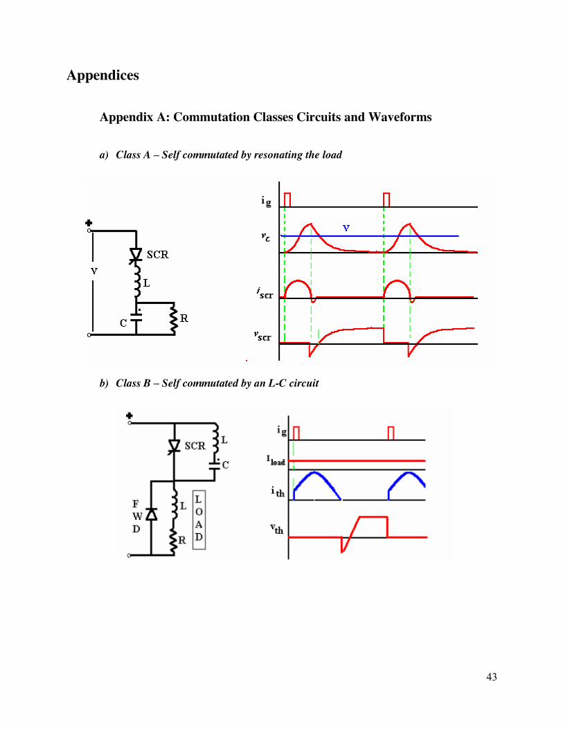
Class A Self commutated by a resonating load
Class B Self commutated by an L-C circuit
Class C C or L-C switched by another load carrying SCR
Class D C or L-C switched by an auxiliary SCR
Class E An external pulse source for commutation
6
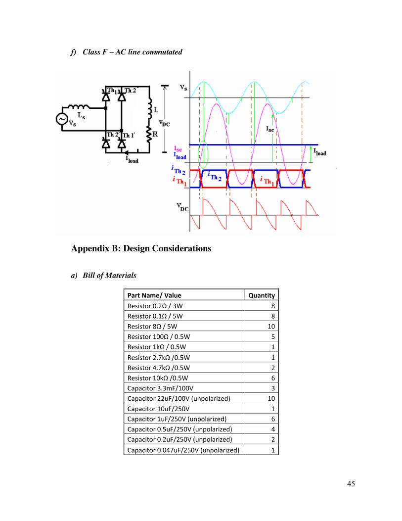
Class F AC line commutation
This experiment will use the Class-C commutation method, which consists of using a
capacitor and a secondary SCR to apply a reverse voltage across the anode and cathode of the
main SCR, forcing it to turn-off. The circuit will force a reverse current through the SCR for a
short period to reduce the anode current to zero. It is necessary to maintain the reverse bias for a
certain time to complete the turnoff. The minimum time that ensures the turn-off is defined as 𝑡 .
7
Apparatus
Definitions
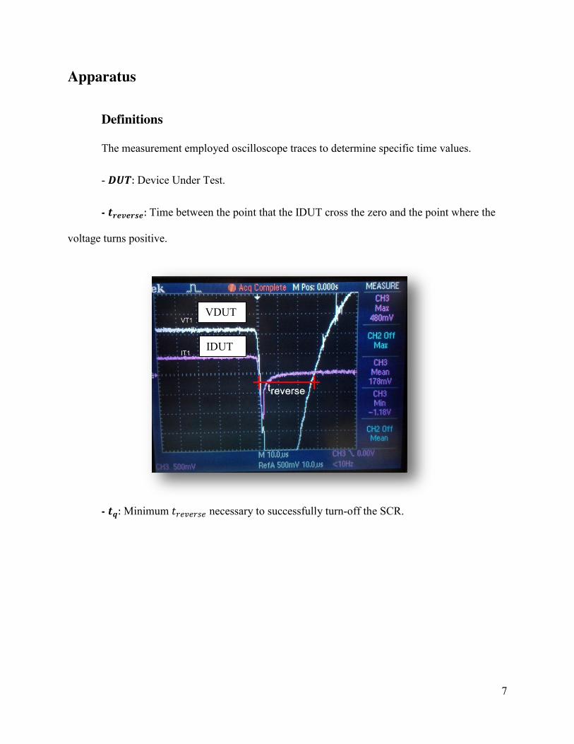
The measurement employed oscilloscope traces to determine specific time values.
- 𝑫𝑼𝑻: Device Under Test.
- 𝒕𝒓𝒆𝒗𝒆𝒓𝒔𝒆: Time between the point that the IDUT cross the zero and the point where the
voltage turns positive.
- 𝒕𝒒: Minimum 𝑡 necessary to successfully turn-off the SCR.
IDUT
VDUT
8
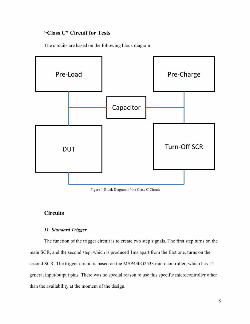
“Class C” Circuit for Tests
The circuits are based on the following block diagram:
Figure 1-Block Diagram of the Class-C Circuit
Circuits
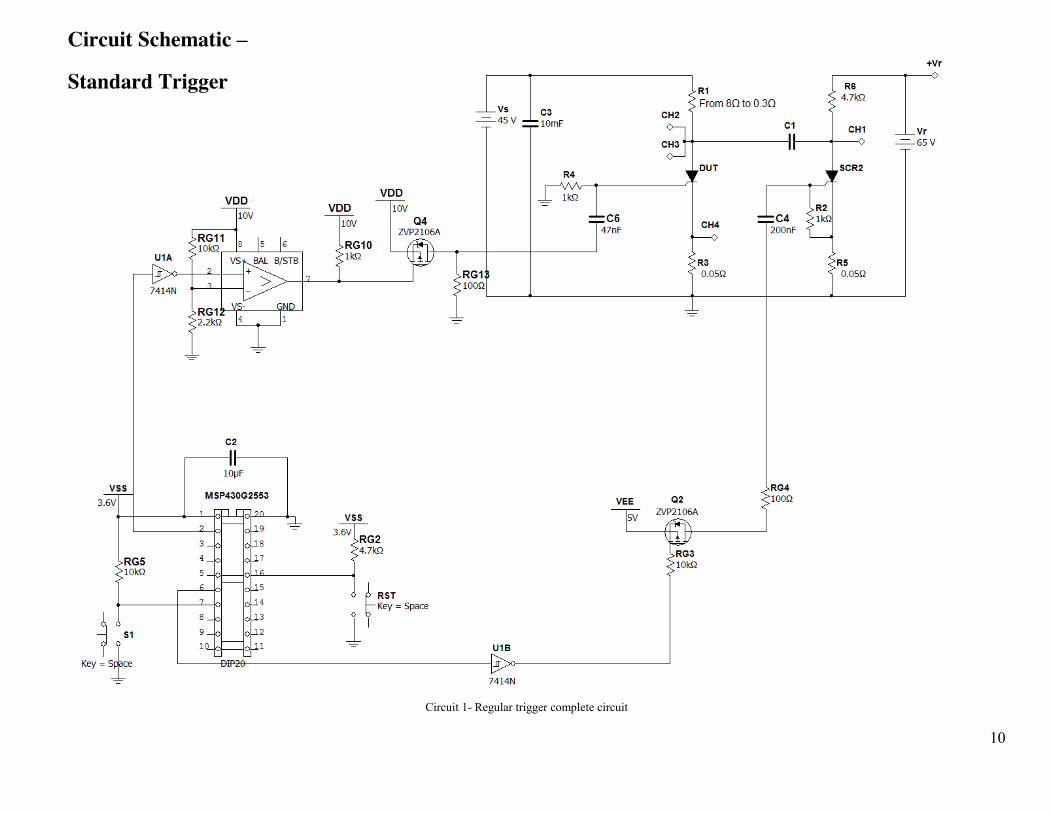
1) Standard Trigger
The function of the trigger circuit is to create two step signals. The first step turns on the
main SCR, and the second step, which is produced 1ms apart from the first one, turns on the
second SCR. The trigger circuit is based on the MSP430G2533 microcontroller, which has 14
general input/output pins. There was no special reason to use this specific microcontroller other
than the availability at the moment of the design.
DUT Turn-Off SCR
Pre-Load
Capacitor
Pre-Charge
9
The gate of both SCRs are capacitive coupled. A step is applied at the MOSFET’s gate of
the main SCR, which results in a pulse that turns on the main SCR. The main SCR (Device
Under Test, or DUT) remains on during 1ms, when the same turn-on procedure occurs at the
second SCR. With the second SCR on, the C1’s voltage is applied across the DUT, forcing it to
turn-off.
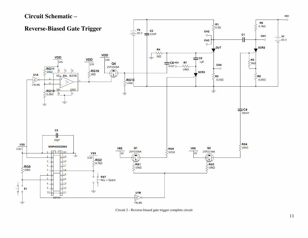
2) Reverse-Biased Gate Trigger
A third SCR is used on the reverse-biasing gate technique. It is triggered at the same time
as the second SCR. Referring to Circuit 2, the capacitor C1 applies the reverse voltage across the
anode, whereas the C5 applies the reverse voltage across the gate of the DUT.
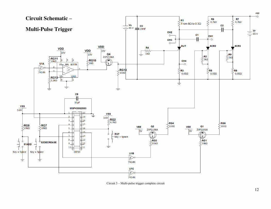
3) Multi-Pulse Trigger
A third SCR is triggered after 𝑡 from the second SCR and applies reverse voltage
across the anode of the DUT. The minimum value of 𝑡 is around 4us, and it can be
increased/decreased by the switches.
10
Circuit 1- Regular trigger complete circuit
Circuit Schematic –
Standard Trigger
11
Circuit 2 - Reverse-biased gate trigger complete circuit
Circuit Schematic –
Reverse-Biased Gate Trigger
12
Circuit 3 – Multi-pulse trigger complete circuit
Circuit Schematic –
Multi-Pulse Trigger
13
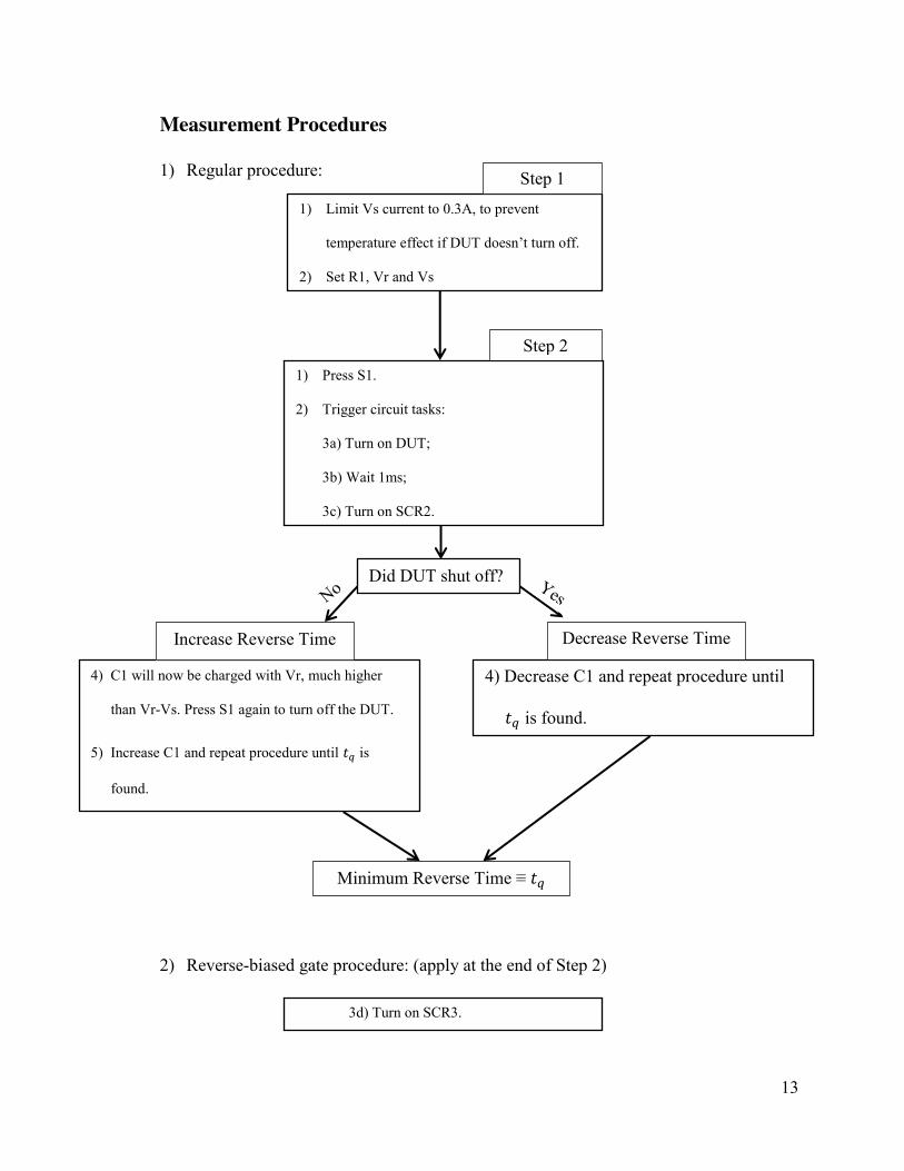
Measurement Procedures
1) Regular procedure:
2) Reverse-biased gate procedure: (apply at the end of Step 2)
3d) Turn on SCR3.
4) C1 will now be charged with Vr, much higher
than Vr-Vs. Press S1 again to turn off the DUT.
5) Increase C1 and repeat procedure until 𝑡 is
found.
4) Decrease C1 and repeat procedure until
𝑡 is found.
Did DUT shut off?
1) Limit Vs current to 0.3A, to prevent
temperature effect if DUT doesn’t turn off.
2) Set R1, Vr and Vs
Step 1
1) Press S1.
2) Trigger circuit tasks:
3a) Turn on DUT;
3b) Wait 1ms;
3c) Turn on SCR2.
Step 2
Increase Reverse Time Decrease Reverse Time
Minimum Reverse Time ≡ 𝑡
14
3) Temperature effect initial tasks:
Devices
The following table lists all the devices and their main parameters.
Part # Manufacturer Package
S6015L TECCOR TO220 S6020L TECCOR TO220 TYN1225 ST MICROELECTRONICS TO220 NTE5558 NTE TO220 25TTS12 INTERNATIONAL RECTIFIER TO220 CS19-08H01 IXYS TO220 MMO62-16IO6 IXYS SOT-227 B NTE5372 NTE TO94 T507 POWEREX TO94 MCC95-16IO1B IXYS TO240 C430PB POWEREX POW-R-DISC
Table 1 – SCRs and their manufacturers and packages.
1) Limit Vs current to 3.5A.
2) Set R1, Vr and Vs.
3) Reduce C1 to a value that does not turn-off the
DUT.
4) Press S1.
5) Leave DUT on for 5 minutes.
15
Part # Irms (A) Itsm (A) VT (V) VDRM (V) tq specified (us)[1]
S6015L 15 225 1.6 600 35 S6020L 20 300 1.6 600 35
TYN1225 25 260 1.6 1225 70
NTE5558 25 300 1.8 800 15 25TTS12 25 300 1.25 1200 110
CS19-08H01 31 180 1.31 800 150
MMO62-16IO6 54 400 1.57 1600 150
NTE5372 135 2450 2.15 1200 30
T507 125 1400 3.2 800 15
MCC95-16IO1B 180 2250 1.5 1600 185
C430PB 1070 8000 2.4 1200 125 Table 2 – SCRs main parameters.
[1] Each manufacturer defines 𝑡 according to their own distinct test conditions. Typical variation is with the amount and duration of the current pulse. For further information, consult the datasheet.
16
Experimental Results
I) Different Kinds of SCRs
There are two kind of SCRs: the “standard” and “fast” devices. In general, the standard
SCRs are classified for phase control applications, whereas the fast devices are for inverters.
The typical 𝑡 from datasheet is from 15us to 35us for fast devices, and 35us to 300us for
standard SCRs.
The following waveforms illustrate the typical current and voltage behavior during the
turn-off for these two kinds of SCRs. The horizontal scale of 25us applies for all the waveforms
below.
1) Standard SCRs
Settings for the experiment: DUT = MCC95, IDUT = 40A, 𝑉 =65V, 𝑉 = 45V.
a) Successful Turn-off: 𝒕𝒓𝒆𝒗𝒆𝒓𝒔𝒆 ≥ 𝒕𝒒
- DUT Current (Vert. 20A/div) - Voltage across DUT (Vert. 1V/div)
17
- DUT Current and Voltage
b) Failure: 𝒕𝒓𝒆𝒗𝒆𝒓𝒔𝒆 < 𝒕𝒒 (near tq)
- DUT Current (Vert. 20A/div) - Voltage across DUT (Vert. 1V/div)
- DUT Current and Voltage
18
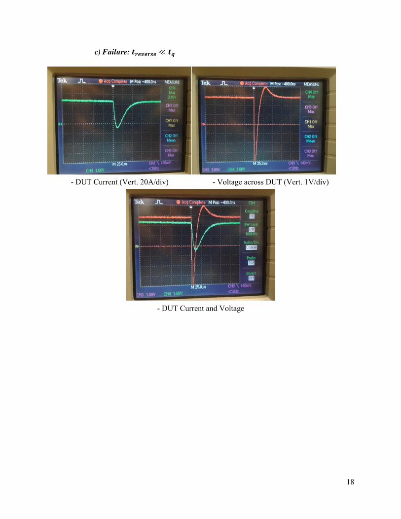
c) Failure: 𝒕𝒓𝒆𝒗𝒆𝒓𝒔𝒆 ≪ 𝒕𝒒
- DUT Current (Vert. 20A/div) - Voltage across DUT (Vert. 1V/div)
- DUT Current and Voltage
19
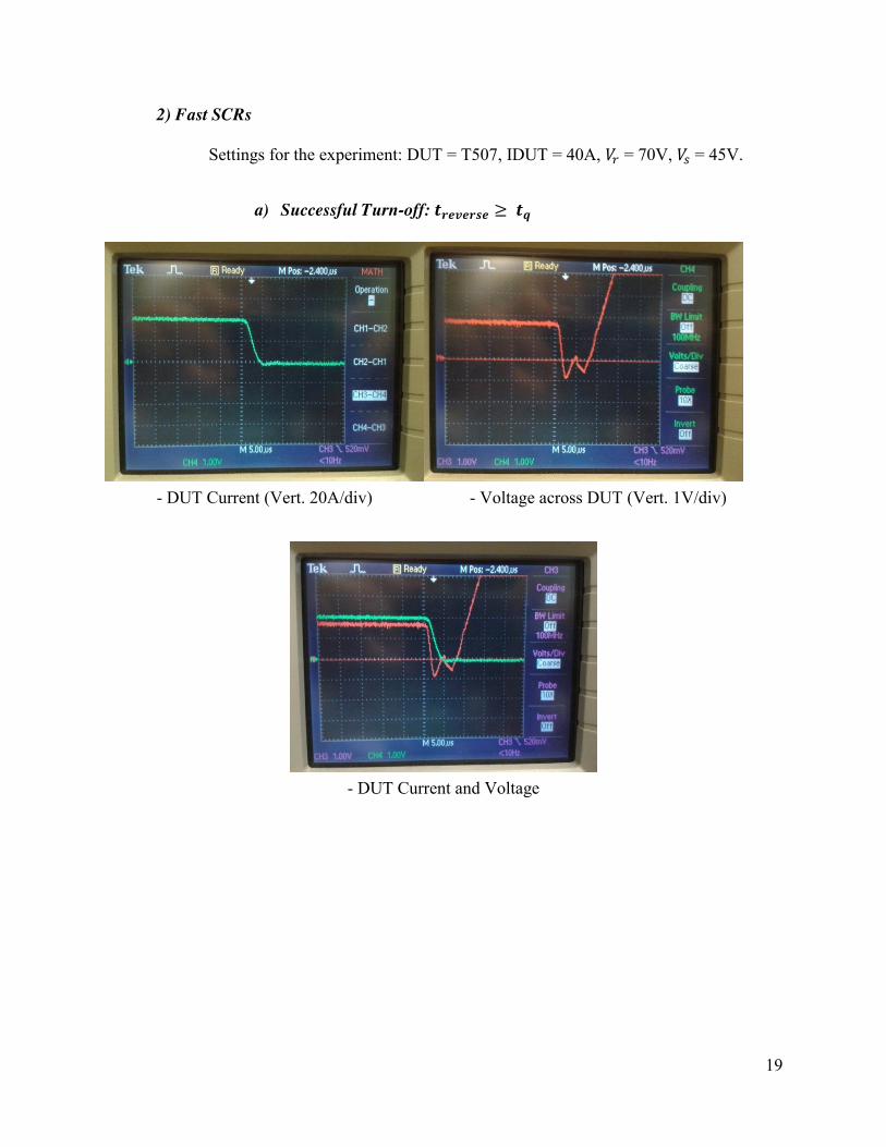
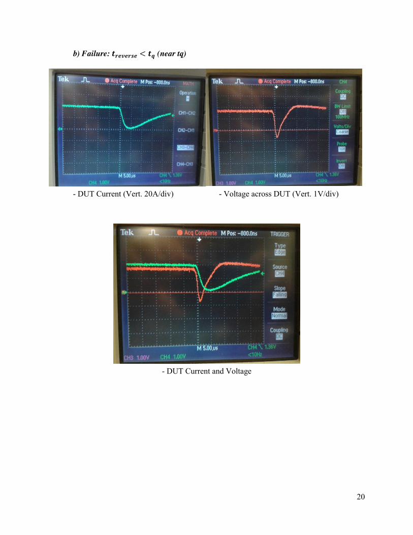
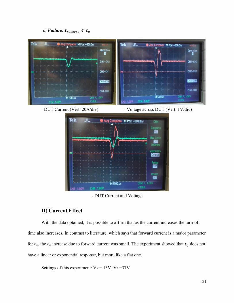
2) Fast SCRs
Settings for the experiment: DUT = T507, IDUT = 40A, 𝑉 = 70V, 𝑉 = 45V.
a) Successful Turn-off: 𝒕𝒓𝒆𝒗𝒆𝒓𝒔𝒆 ≥ 𝒕𝒒
- DUT Current (Vert. 20A/div) - Voltage across DUT (Vert. 1V/div)
- DUT Current and Voltage
20
b) Failure: 𝒕𝒓𝒆𝒗𝒆𝒓𝒔𝒆 < 𝒕𝒒 (near tq)
- DUT Current (Vert. 20A/div) - Voltage across DUT (Vert. 1V/div)
- DUT Current and Voltage
21
c) Failure: 𝒕𝒓𝒆𝒗𝒆𝒓𝒔𝒆 ≪ 𝒕𝒒
- DUT Current (Vert. 20A/div) - Voltage across DUT (Vert. 1V/div)
- DUT Current and Voltage
II) Current Effect
With the data obtained, it is possible to affirm that as the current increases the turn-off
time also increases. In contrast to literature, which says that forward current is a major parameter
for 𝑡 , the 𝑡 increase due to forward current was small. The experiment showed that 𝑡 does not
have a linear or exponential response, but more like a flat one.
Settings of this experiment: Vs = 13V, Vr =37V
22
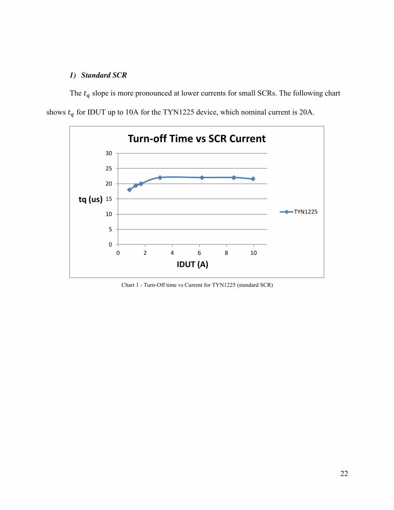
1) Standard SCR
The 𝑡 slope is more pronounced at lower currents for small SCRs. The following chart
shows 𝑡 for IDUT up to 10A for the TYN1225 device, which nominal current is 20A.
Chart 1 - Turn-Off time vs Current for TYN1225 (standard SCR)
0
5
10
15
20
25
30
0 2 4 6 8 10
tq (us)
IDUT (A)
Turn-off Time vs SCR Current
TYN1225
23
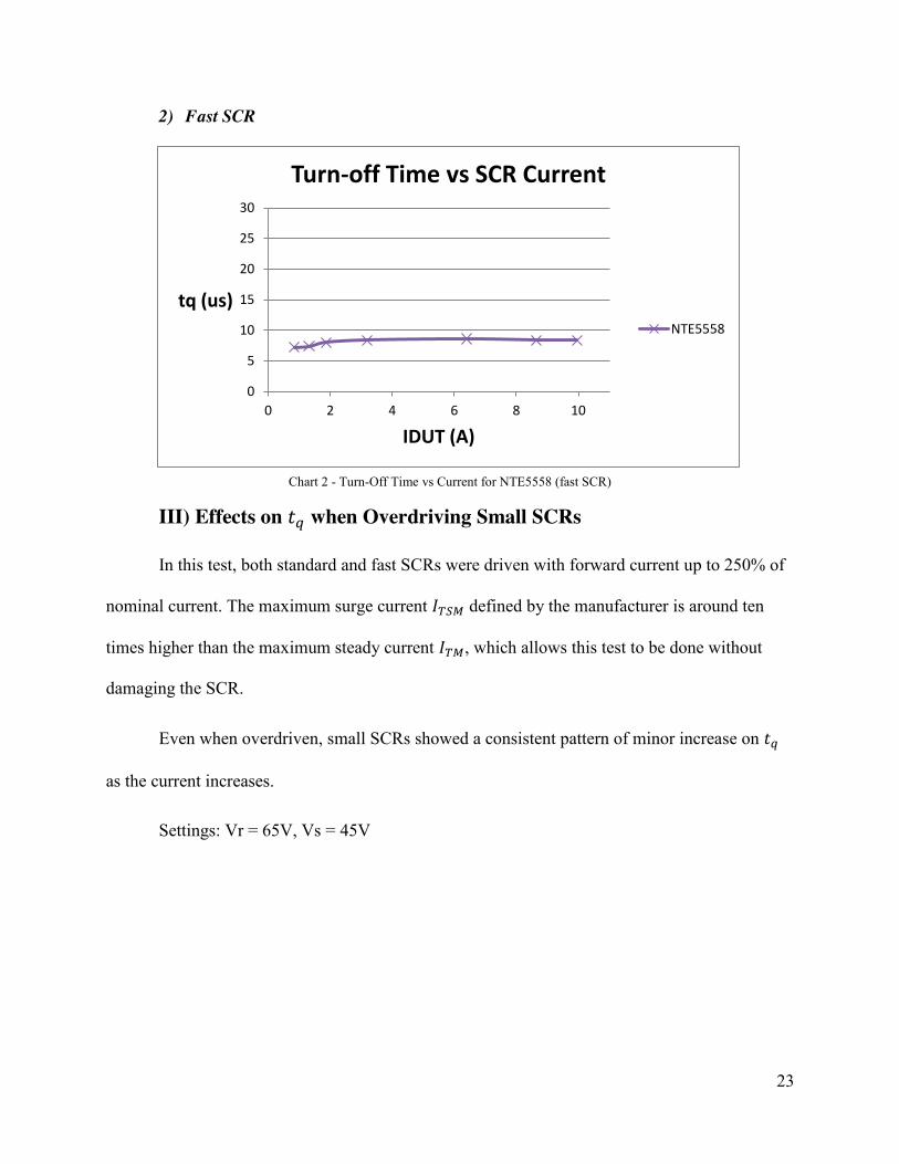
2) Fast SCR
Chart 2 - Turn-Off Time vs Current for NTE5558 (fast SCR)
III) Effects on 𝑡 when Overdriving Small SCRs
In this test, both standard and fast SCRs were driven with forward current up to 250% of
nominal current. The maximum surge current 𝐼 defined by the manufacturer is around ten
times higher than the maximum steady current 𝐼 , which allows this test to be done without
damaging the SCR.
Even when overdriven, small SCRs showed a consistent pattern of minor increase on 𝑡
as the current increases.
Settings: Vr = 65V, Vs = 45V
0
5
10
15
20
25
30
0 2 4 6 8 10
tq (us)
IDUT (A)
Turn-off Time vs SCR Current
NTE5558
24
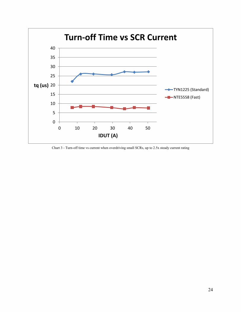
Chart 3 - Turn-off time vs current when overdriving small SCRs, up to 2.5x steady current rating
0
5
10
15
20
25
30
35
40
0 10 20 30 40 50
tq (us)
IDUT (A)
Turn-off Time vs SCR Current
TYN1225 (Standard)
NTE5558 (Fast)

25
IV) Key Design Factors for Small SCRs
1) Total capacitor charge available
In the beginning, there was a suspicion that the available charge at the capacitor might be
critical to turn-off the SCR. To measure the capacitor charge effect, the SCR was set at a specific
current and C was increased to higher values. The minimum 𝑉 necessary to turn-off would
determine the minimum charge necessary 𝑄 = 𝐶 ∗ 𝑉 to turn-off the SCR for a given
capacitance. The tests were done using small SCRs.
Settings: DUT = TYN1225, Vs = 12V, IDUT = 2A
C (uF) Minimum Vc to turn-off (V)
Capacitor Charge (uC)
Q relative (%)
Turned-Off?
21.9 35 766.5 100.00 Yes 35.4 22.6 800.04 104.38 Yes 50.8 18.1 919.48 119.96 Yes 65 16.5 1072.5 139.92 Yes
86.7 14.7 1274.49 166.27 Yes Table 3 – Charge effect on the turn-off for the TYN1225.
Settings: DUT = S6015L, Vs = 12V, IDUT = 2A
C (uF) Minimum Vc to turn-off (V)
Capacitor Charge (uC)
Q relative (%)
Turned-Off?
33.3 30.8 1025.64 100.00 Yes 25.2 43.1 1086.12 105.90 Yes 22.7 50.4 1144.08 111.55 Yes 18.9 67.9 1283.31 125.12 Yes 16.3 92.9 1514.27 147.64 Yes
Table 4 – Charge effect on the turn-off for the S6015L
The total available capacitor charge is not critical to turn-off the SCR, since different Q
were needed to turn-off the SCR at a given capacitance for small SCRs.

26
2) Capacitor time constant
Empirically, it was found that the capacitor time constant can be assumed as 𝜏 = 𝑅 ∗
𝐶1 without much deviance. During the regular measurements, for example, if the 𝑅 was
decreased to get higher currents, the C1 capacitance had to be increased to achieve the same
𝑡 . This was a clue that the turn-off was somewhat related to C1’s time constant.
This table illustrates 𝑡 and 𝜏 for a small SCR.
Settings: DUT = TYN1225, Vs = 13V, Vr = 37V
IT1 (A) 𝒕𝒒 (us) Rload (ohms) Capacitance
(uF) 𝝉 (us) 𝒕𝒒/𝝉
0.85 18.00 20.00 1.07 21.40 0.84 1.32 19.40 10.90 2.05 22.35 0.87 1.69 20.00 8.00 2.88 23.04 0.87 3.10 22.00 4.00 5.87 23.48 0.94 6.20 22.00 1.60 15.00 24.00 0.92 8.55 22.00 1.00 26.00 26.00 0.85 9.96 21.60 0.80 34.40 27.52 0.78
Table 5 – 𝑡 and time constant necessary to turn-off an SCR at a given current.
27
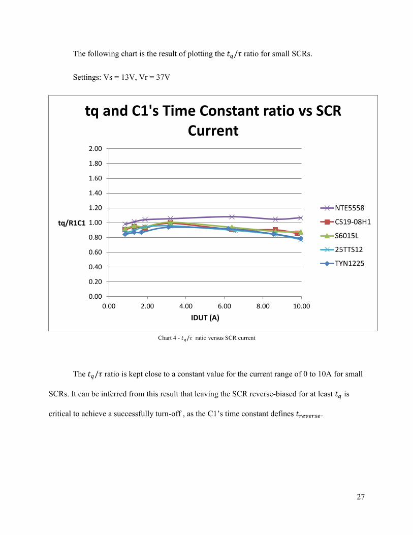
The following chart is the result of plotting the 𝑡 /𝜏 ratio for small SCRs.
Settings: Vs = 13V, Vr = 37V
Chart 4 - 𝑡 /𝜏 ratio versus SCR current
The 𝑡 /𝜏 ratio is kept close to a constant value for the current range of 0 to 10A for small
SCRs. It can be inferred from this result that leaving the SCR reverse-biased for at least 𝑡 is
critical to achieve a successfully turn-off , as the C1’s time constant defines 𝑡 .
0.00
0.20
0.40
0.60
0.80
1.00
1.20
1.40
1.60
1.80
2.00
0.00 2.00 4.00 6.00 8.00 10.00
tq/R1C1
IDUT (A)
tq and C1's Time Constant ratio vs SCR Current
NTE5558
CS19-08H1
S6015L
25TTS12
TYN1225
28
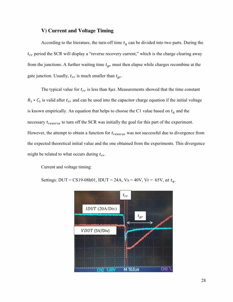
V) Current and Voltage Timing
According to the literature, the turn-off time 𝑡 can be divided into two parts. During the
𝑡 period the SCR will display a “reverse recovery current,” which is the charge clearing away
from the junctions. A further waiting time 𝑡 must then elapse while charges recombine at the
gate junction. Usually, 𝑡 is much smaller than 𝑡 .
The typical value for 𝑡 is less than 8𝜇𝑠. Measurements showed that the time constant
𝑅 ∗ 𝐶 is valid after 𝑡 and can be used into the capacitor charge equation if the initial voltage
is known empirically. An equation that helps to choose the C1 value based on 𝑡 and the
necessary 𝑡 to turn off the SCR was initially the goal for this part of the experiment.
However, the attempt to obtain a function for 𝑡 was not successful due to divergence from
the expected theoretical initial value and the one obtained from the experiments. This divergence
might be related to what occurs during 𝑡 .
Current and voltage timing:
Settings: DUT = CS19-08h01, IDUT = 24A, Vs = 40V, Vr = 65V, 𝑎𝑡 𝑡 .
𝑡
𝑡 𝐼𝐷𝑈𝑇 (20A/Div)
𝑉𝐷𝑈𝑇 (5V/Div)
29
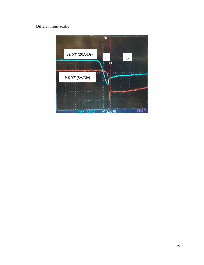
Different time scale:
𝑡 𝑡 𝐼𝐷𝑈𝑇 (20A/Div)
𝑉𝐷𝑈𝑇 (5V/Div)

30
VI) Temperature Effect
Most manufacturers specify the turn-off time for a junction temperature equals to 125°C,
as worst case scenario. To study the temperature effect, the SCR was warmed up with 3.5A for 5
minutes before the test. Below are the case temperatures for both devices during the test.
Device Tcase (°C) C430PB 32
T507088074AQ 45
1) Standard SCR
Settings: DUT = C430PB, Vs = 45V, Vr = 65V
IDUT (A) Regular 𝒕𝒒(us) Warmed up 𝒕𝒒 (us)
𝒕𝒒increase (%)
7.2 22 23.6 7.27 12 22.8 28.4 24.56 16 26 30 15.38
24.8 26 30 15.38 32.8 26 30.8 18.46 38.4 26.8 31.6 17.91 45.6 26.8 32.4 20.90 50.4 27.2 32.8 20.59
Table 6- 𝑡 increase with the temperature for standard SCR
31
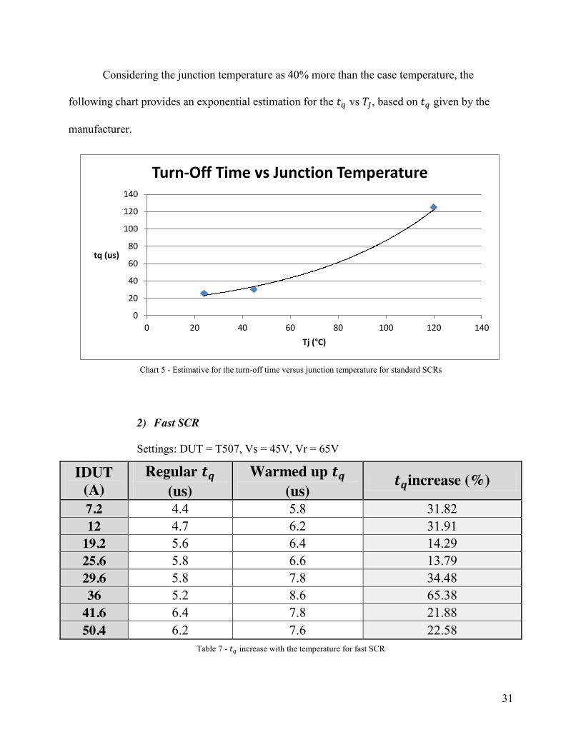
Considering the junction temperature as 40% more than the case temperature, the
following chart provides an exponential estimation for the 𝑡 vs 𝑇 , based on 𝑡 given by the
manufacturer.
Chart 5 - Estimative for the turn-off time versus junction temperature for standard SCRs
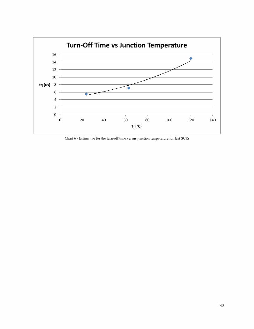
2) Fast SCR
Settings: DUT = T507, Vs = 45V, Vr = 65V
IDUT (A)
Regular 𝒕𝒒 (us)
Warmed up 𝒕𝒒 (us)
𝒕𝒒increase (%)
7.2 4.4 5.8 31.82 12 4.7 6.2 31.91
19.2 5.6 6.4 14.29 25.6 5.8 6.6 13.79 29.6 5.8 7.8 34.48 36 5.2 8.6 65.38
41.6 6.4 7.8 21.88 50.4 6.2 7.6 22.58
Table 7 - 𝑡 increase with the temperature for fast SCR
0
20
40
60
80
100
120
140
0 20 40 60 80 100 120 140
tq (us)
Tj (°C)
Turn-Off Time vs Junction Temperature
32
Chart 6 - Estimative for the turn-off time versus junction temperature for fast SCRs
0
2
4
6
8
10
12
14
16
0 20 40 60 80 100 120 140
tq (us)
Tj (°C)
Turn-Off Time vs Junction Temperature

33
VII) Power Size Effect
The following table defines the classes for SCRs which turn-off times were measured.
Power Class Steady Current Range Small Less than 25A
Moderate Between 25A and 150A High More than 150A
Table 8 - Power classification
1) Small SCRs
Chart 7 - 𝑡 vs current for small SCRs
0
5
10
15
20
25
30
35
40
0 2 4 6 8 10
tq (us)
IDUT (A)
Turn-Off Time vs SCR Current
S6015L (Standard)
CS19-08H1 (Standard)
25TTS12 (Standard)
TYN1225 (Standard)
NTE5558 (Fast)
34
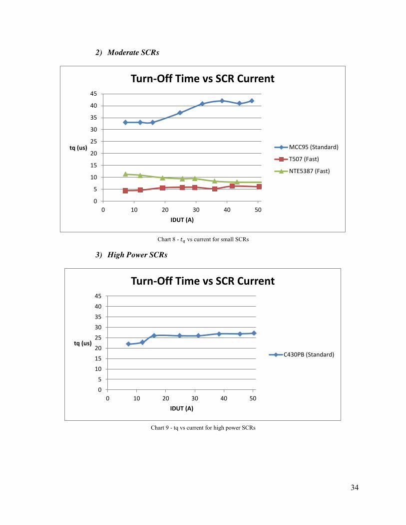
2) Moderate SCRs
Chart 8 - 𝑡 vs current for small SCRs
3) High Power SCRs
Chart 9 - tq vs current for high power SCRs
0
5
10
15
20
25
30
35
40
45
0 10 20 30 40 50
tq (us)
IDUT (A)
Turn-Off Time vs SCR Current
MCC95 (Standard)
T507 (Fast)
NTE5387 (Fast)
05
1015202530354045
0 10 20 30 40 50
tq (us)
IDUT (A)
Turn-Off Time vs SCR Current
C430PB (Standard)
35
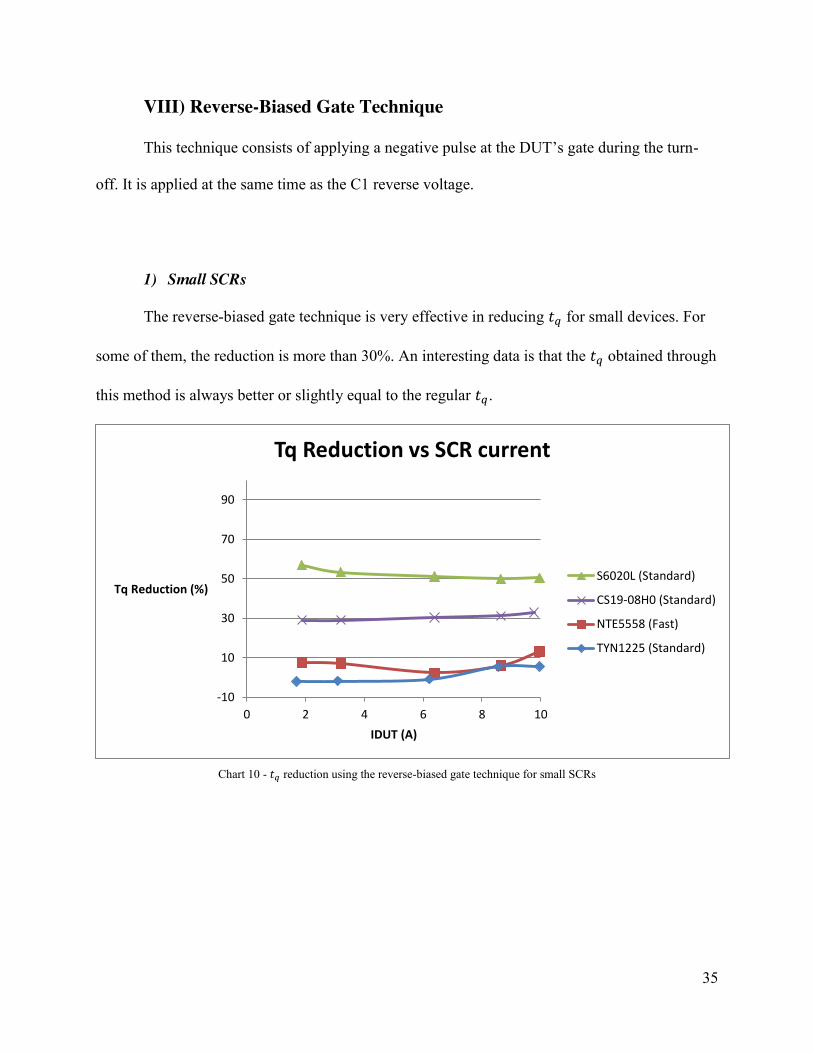
VIII) Reverse-Biased Gate Technique
This technique consists of applying a negative pulse at the DUT’s gate during the turn-
off. It is applied at the same time as the C1 reverse voltage.
1) Small SCRs
The reverse-biased gate technique is very effective in reducing 𝑡 for small devices. For
some of them, the reduction is more than 30%. An interesting data is that the 𝑡 obtained through
this method is always better or slightly equal to the regular 𝑡 .
Chart 10 - 𝑡 reduction using the reverse-biased gate technique for small SCRs
-10
10
30
50
70
90
0 2 4 6 8 10
Tq Reduction (%)
IDUT (A)
Tq Reduction vs SCR current
S6020L (Standard)
CS19-08H0 (Standard)
NTE5558 (Fast)
TYN1225 (Standard)
36
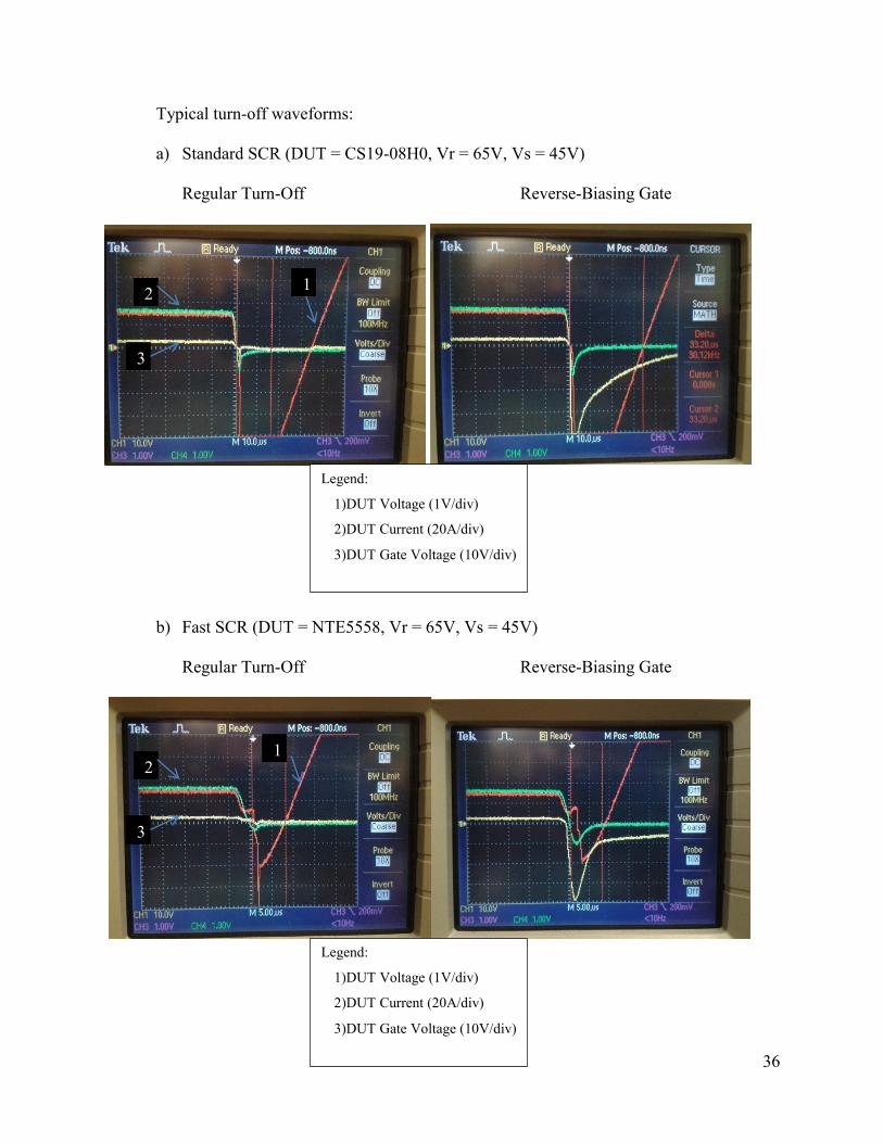
Typical turn-off waveforms:
a) Standard SCR (DUT = CS19-08H0, Vr = 65V, Vs = 45V)
Regular Turn-Off Reverse-Biasing Gate
b) Fast SCR (DUT = NTE5558, Vr = 65V, Vs = 45V)
Regular Turn-Off Reverse-Biasing Gate
Legend:
1)DUT Voltage (1V/div)
2)DUT Current (20A/div)
3)DUT Gate Voltage (10V/div)
1 2
3
Legend:
1)DUT Voltage (1V/div)
2)DUT Current (20A/div)
3)DUT Gate Voltage (10V/div)
1 2
3
37
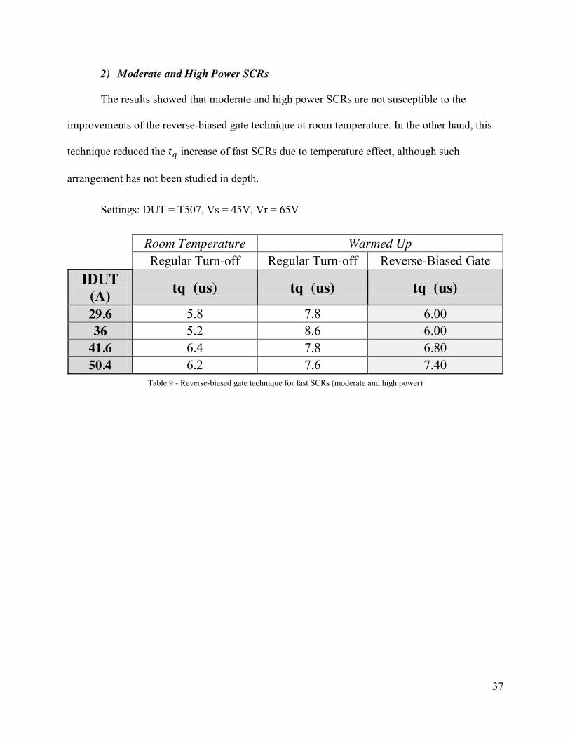
2) Moderate and High Power SCRs
The results showed that moderate and high power SCRs are not susceptible to the
improvements of the reverse-biased gate technique at room temperature. In the other hand, this
technique reduced the 𝑡 increase of fast SCRs due to temperature effect, although such
arrangement has not been studied in depth.
Settings: DUT = T507, Vs = 45V, Vr = 65V
Room Temperature Warmed Up
Regular Turn-off Regular Turn-off Reverse-Biased Gate
IDUT (A) tq (us) tq (us) tq (us) 29.6 5.8 7.8 6.00 36 5.2 8.6 6.00
41.6 6.4 7.8 6.80 50.4 6.2 7.6 7.40
Table 9 - Reverse-biased gate technique for fast SCRs (moderate and high power)

38
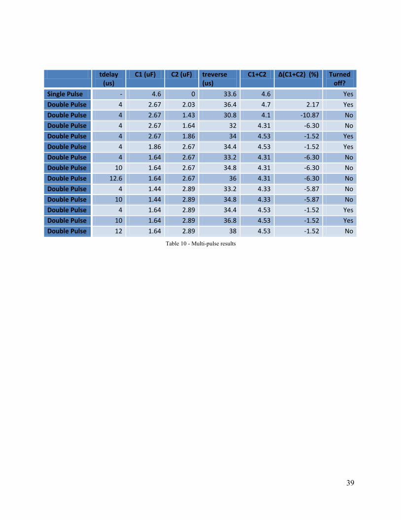
IX) Multi-Pulse Attempt
The multi-pulse technique consists of dividing the reverse pulse across the anode into
two. The first SCR begins the turn-off procedure and after 𝑡 a second SCR applies the
second pulse. Below are the waveforms obtained when using this method. 𝑡 minimum value
is around 4us, and it can be increased/decreased by using the switches on the circuit.
Figure 2 - Waveforms for the multi-pulse triggering method
First, a single pulse was used to define the default 𝑡 . Then, different settings of 𝑡
and capacitance combinations were used to try to achieve a scenario where a 𝑡 reduction could
be seen. This method did not show significant reduction on the turn-off time for small SCRs
running low currents.
Settings: DUT = S6020L, SCR2 = S6020L, SCR3 = TYN1225, Vs = 13V,
Vr = 37V, IDUT = 1.5A (steady), all circuit on protoboard.
Legend:
1) DUT Voltage
2) SCR3 Current
3) SCR2 Current
4) DUT Current
𝑡 : time between 3) and 2)
4
2 3
1
39
tdelay (us)
C1 (uF) C2 (uF) treverse (us)
C1+C2 Δ(C1+C2) (%) Turned off?
Single Pulse - 4.6 0 33.6 4.6 Yes Double Pulse 4 2.67 2.03 36.4 4.7 2.17 Yes Double Pulse 4 2.67 1.43 30.8 4.1 -10.87 No Double Pulse 4 2.67 1.64 32 4.31 -6.30 No Double Pulse 4 2.67 1.86 34 4.53 -1.52 Yes Double Pulse 4 1.86 2.67 34.4 4.53 -1.52 Yes Double Pulse 4 1.64 2.67 33.2 4.31 -6.30 No Double Pulse 10 1.64 2.67 34.8 4.31 -6.30 No Double Pulse 12.6 1.64 2.67 36 4.31 -6.30 No Double Pulse 4 1.44 2.89 33.2 4.33 -5.87 No Double Pulse 10 1.44 2.89 34.8 4.33 -5.87 No Double Pulse 4 1.64 2.89 34.4 4.53 -1.52 Yes Double Pulse 10 1.64 2.89 36.8 4.53 -1.52 Yes Double Pulse 12 1.64 2.89 38 4.53 -1.52 No
Table 10 - Multi-pulse results
40
X) Suggestion for Further Work
The results obtained were promising about impeding the increase of 𝑡 on fast SCRs due
to temperature effect with the reverse-biased gate technique. Also, temperature effect was not
studied for small SCRs. More data would give a better understanding on these two topics.
The effect of overdriving small SCRs was studied using forward current pulses up to 2.5x
the steady current rating. This test could be performed by applying forward current up to 𝐼 ,
which is usually more than 10x the steady current rating.
According to the literature, the rate can influence the turn-off. The rate of the
reapplied voltage could not be controlled by the employed circuit; it was defined by the
capacitor, the time constant, and initial/final voltage of the charge. Its typical value was below
2V/𝜇𝑠. An improved circuit version with control would be able to see how is the effect of
on 𝑡 .
41
Summary
The focus of this report was to study the turn-off conditions for power SCRs. The devices
employed in this experiment can be divided in two classes: fast and standard SCRs. There is a
significant 𝑡 difference between these two classes. In all tests with the various SCRs the
measured 𝑡 was always equal or less than the specified value on the datasheet.
In contrast to literature, which says that forward current is a major parameter on 𝑡 ,
applying steady state current in the ratio from 10 to 120% of the steady current rating resulted
only into a minor increase on 𝑡 , around 10 to 30%. The 𝑡 response for the current does not
comply with a linear or exponential trend. Instead, its response can be considered flat between 20
to 80% of average steady current rating. This behavior can be extended without much deviation
for SCRs of all power classes.
The effect on 𝑡 when overdriving small SCRs was studied. Even with forward current at
2.5x of steady state current rating, the 𝑡 had consistent response with operation under regular
settings.
Also, there was a suspicion that the available charge at the capacitor might be critical to
turn off the SCR. The tests results showed that the charge is not a critical factor, but the C1 time
constant. The 𝑡 /𝜏 ratio is kept almost constant for small SCRs up to 50% of steady current
rating.
The turn-off time is directly related to the junction temperature. As the temperature
increases, the SCR will need to stay reverse-biased for a longer time during the turn-off, and in
some cases, the 𝑡 increase can be more than 30%. An appropriate heat sink or dissipation
system to cool down the SCR can impede the increase of 𝑡 .
42
The reverse-biased gate technique was found to be an effective way to reduce the 𝑡 for
some small SCRs, especially the standard ones. No significant gain has been seen with the
moderate and high power SCRs at room temperature. However, in the real world situation where
the SCR is hot, the reverse-biased gate technique reduced the 𝑡 increase of fast SCRs due to
temperature effect.
The multi-pulse technique did not show significant 𝑡 reduction for small SCRs at low
currents. As this method was tested with one small SCR, the influence of it on 𝑡 for moderate
and high power SCRs is unknown. Despite the small influence on 𝑡 , the multi-pulse trigger
allows to split the single-pulse capacitance into two smaller ones.
43
Appendices
Appendix A: Commutation Classes Circuits and Waveforms
a) Class A – Self commutated by resonating the load
b) Class B – Self commutated by an L-C circuit

44
c) Class C – C or LC switched by another load-carrying SCR
d) Class D – LC or C switched by an auxiliary SCR
e) Class E – External pulse source for commutation
45
f) Class F – AC line commutated
Appendix B: Design Considerations
a) Bill of Materials
Part Name/ Value Quantity Resistor 0.2Ω / 3W 8 Resistor 0.1Ω / 5W 8 Resistor 8Ω / 5W 10 Resistor 100Ω / 0.5W 5 Resistor 1kΩ / 0.5W 1 Resistor 2.7kΩ /0.5W 1 Resistor 4.7kΩ /0.5W 2 Resistor 10kΩ /0.5W 6 Capacitor 3.3mF/100V 3 Capacitor 22uF/100V (unpolarized) 10 Capacitor 10uF/250V 1 Capacitor 1uF/250V (unpolarized) 6 Capacitor 0.5uF/250V (unpolarized) 4 Capacitor 0.2uF/250V (unpolarized) 2 Capacitor 0.047uF/250V (unpolarized) 1
46
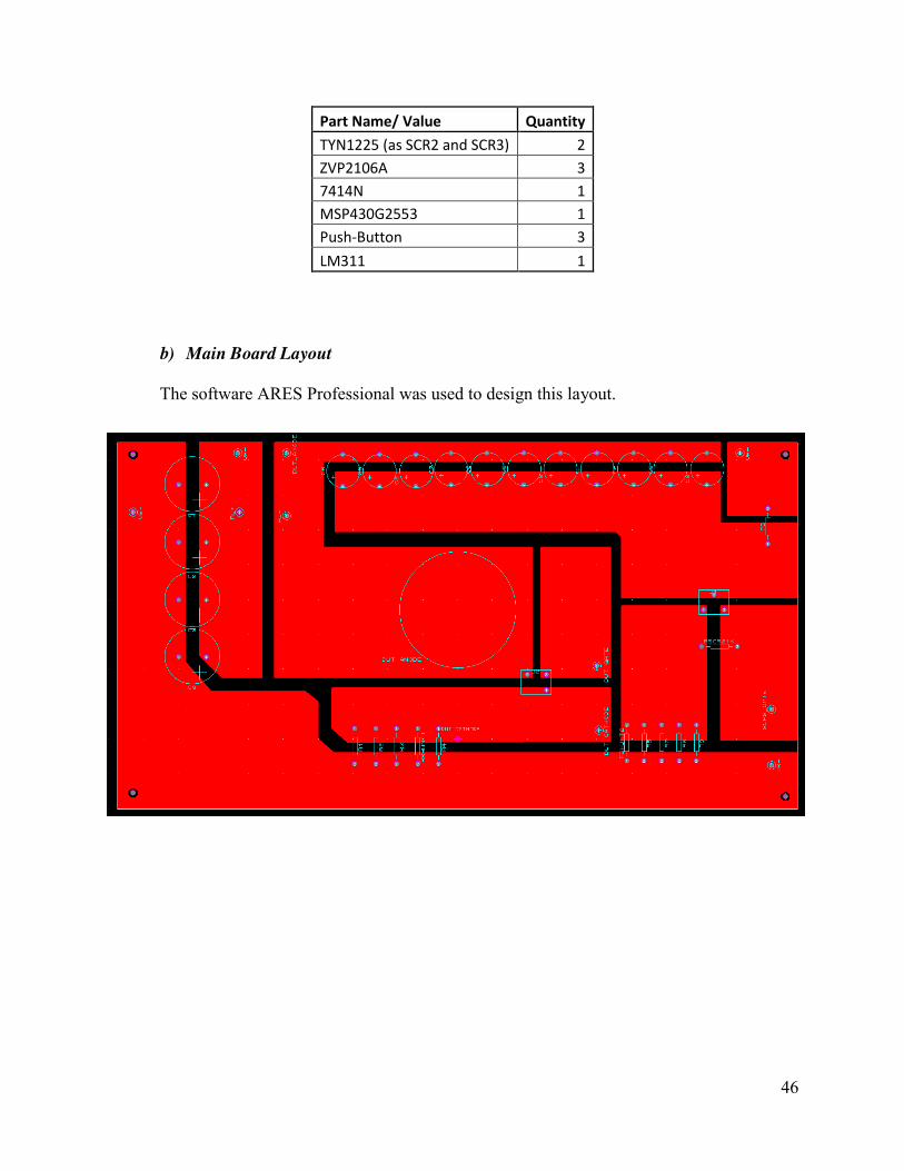
Part Name/ Value Quantity TYN1225 (as SCR2 and SCR3) 2 ZVP2106A 3 7414N 1 MSP430G2553 1 Push-Button 3 LM311 1
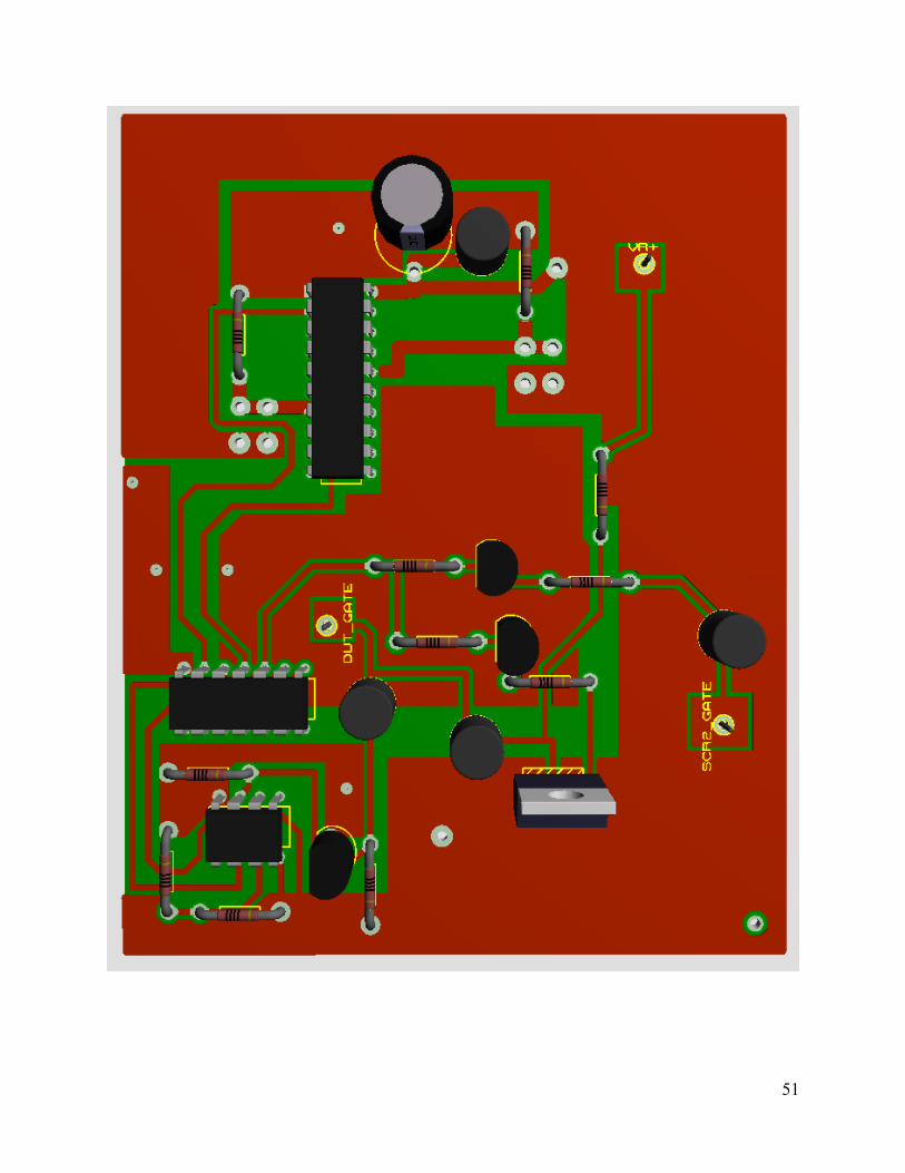
b) Main Board Layout
The software ARES Professional was used to design this layout.
47
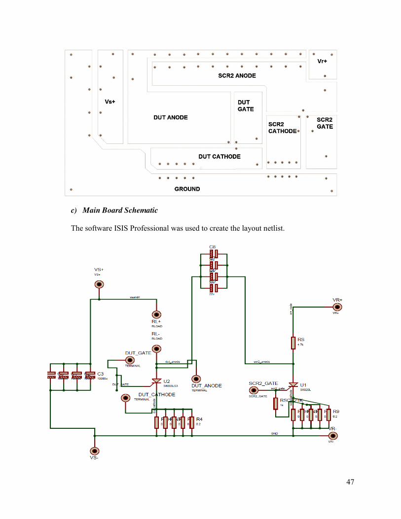
c) Main Board Schematic
The software ISIS Professional was used to create the layout netlist.
48
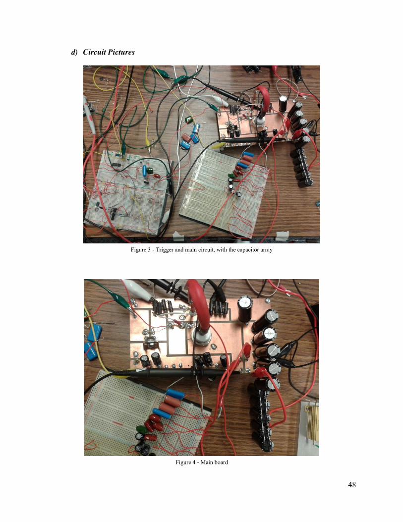
d) Circuit Pictures
Figure 3 - Trigger and main circuit, with the capacitor array
Figure 4 - Main board
49
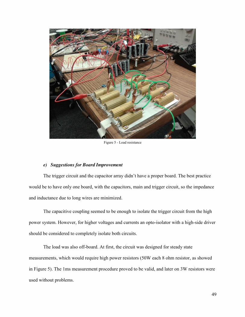
Figure 5 - Load resistance
e) Suggestions for Board Improvement
The trigger circuit and the capacitor array didn’t have a proper board. The best practice
would be to have only one board, with the capacitors, main and trigger circuit, so the impedance
and inductance due to long wires are minimized.
The capacitive coupling seemed to be enough to isolate the trigger circuit from the high
power system. However, for higher voltages and currents an opto-isolator with a high-side driver
should be considered to completely isolate both circuits.
The load was also off-board. At first, the circuit was designed for steady state
measurements, which would require high power resistors (50W each 8 ohm resistor, as showed
in Figure 5). The 1ms measurement procedure proved to be valid, and later on 3W resistors were
used without problems.
50
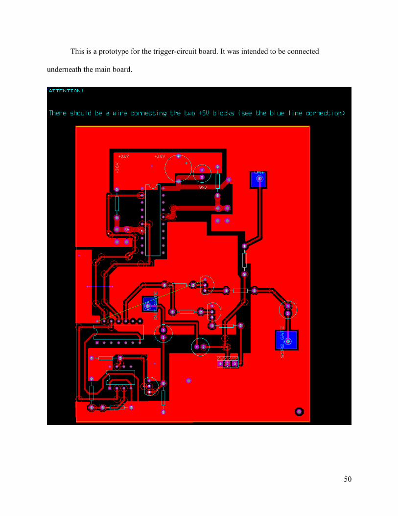
This is a prototype for the trigger-circuit board. It was intended to be connected
underneath the main board.
51
52
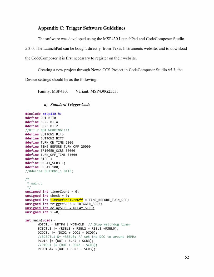
Appendix C: Trigger Software Guidelines
The software was developed using the MSP430 LaunchPad and CodeComposer Studio
5.3.0. The LaunchPad can be bought directly from Texas Instruments website, and to download
the CodeComposer it is first necessary to register on their website.
Creating a new project through New> CCS Project in CodeComposer Studio v5.3, the
Device settings should be as the following:
Family: MSP430; Variant: MSP430G2553;
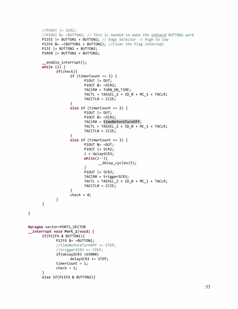
a) Standard Trigger Code
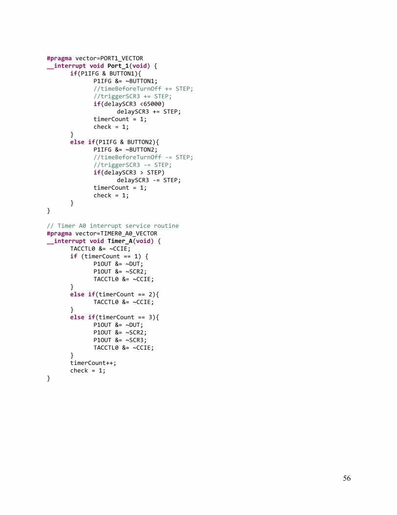
#include <msp430.h> #define DUT BIT0 #define SCR2 BIT4 #define SCR3 BIT2 //BIT 7 NOT WORKING!!!! #define BUTTON1 BIT5 #define BUTTON2 BIT7 #define TURN_ON_TIME 2000 #define TIME_BEFORE_TURN_OFF 20000 #define TRIGGER_SCR3 50000 #define TURN_OFF_TIME 35000 #define STEP 1 #define DELAY_SCR3 1; #define DELAY 100; //#define BUTTON1_1 BIT3; /* * main.c */ unsigned int timerCount = 0; unsigned int check = 0; unsigned int timeBeforeTurnOff = TIME_BEFORE_TURN_OFF; unsigned int triggerSCR3 = TRIGGER_SCR3; unsigned int delaySCR3 = DELAY_SCR3; unsigned int i =0; int main(void) { WDTCTL = WDTPW | WDTHOLD; // Stop watchdog timer BCSCTL1 |= (RSEL3 + RSEL2 + RSEL1 +RSEL0); DCOCTL |= (DCO2 + DCO1 + DCO0); //BCSCTL1 &= ~RSEL0; // set the DCO to around 10MHz P1DIR |= (DUT + SCR2 + SCR3); //P1OUT |= (DUT + SCR2 + SCR3); P1OUT &= ~(DUT + SCR2 + SCR3);
53
//P1OUT |= SCR2; //P1OUT &= ~BUTTON2; // This is needed to make the onboard BUTTON1 work P1IES |= BUTTON1 + BUTTON2; // Edge Selector -> High to low P1IFG &= ~(BUTTON1 + BUTTON2); //Clear the flag interrupt P1IE |= BUTTON1 + BUTTON2; P1REN |= BUTTON1 + BUTTON2; __enable_interrupt(); while (1) { if(check){ if (timerCount == 1) { P1OUT |= DUT; P1OUT &= ~SCR2; TACCR0 = TURN_ON_TIME; TACTL = TASSEL_2 + ID_0 + MC_1 + TACLR; TACCTL0 = CCIE; } else if (timerCount == 2) { P1OUT |= DUT; P1OUT &= ~SCR2; TACCR0 = timeBeforeTurnOff; TACTL = TASSEL_2 + ID_0 + MC_1 + TACLR; TACCTL0 = CCIE; } else if (timerCount == 3) { P1OUT &= ~DUT; P1OUT |= SCR2; i = delaySCR3; while(i--){ __delay_cycles(5); } P1OUT |= SCR3; TACCR0 = triggerSCR3; TACTL = TASSEL_2 + ID_0 + MC_1 + TACLR; TACCTL0 = CCIE; } check = 0; } } } #pragma vector=PORT1_VECTOR __interrupt void Port_1(void) { if(P1IFG & BUTTON1){ P1IFG &= ~BUTTON1; //timeBeforeTurnOff += STEP; //triggerSCR3 += STEP; if(delaySCR3 <65000) delaySCR3 += STEP; timerCount = 1; check = 1; } else if(P1IFG & BUTTON2){
54
P1IFG &= ~BUTTON2; //timeBeforeTurnOff -= STEP; //triggerSCR3 -= STEP; if(delaySCR3 > STEP) delaySCR3 -= STEP; timerCount = 1; check = 1; } } // Timer A0 interrupt service routine #pragma vector=TIMER0_A0_VECTOR __interrupt void Timer_A(void) { TACCTL0 &= ~CCIE; if (timerCount == 1) { P1OUT |= DUT; P1OUT &= ~SCR2; TACCTL0 &= ~CCIE; } else if(timerCount == 2){ TACCTL0 &= ~CCIE; } else if(timerCount == 3){ P1OUT &= ~DUT; P1OUT &= ~SCR2; P1OUT &= ~SCR3; TACCTL0 &= ~CCIE; } timerCount++; check = 1; }
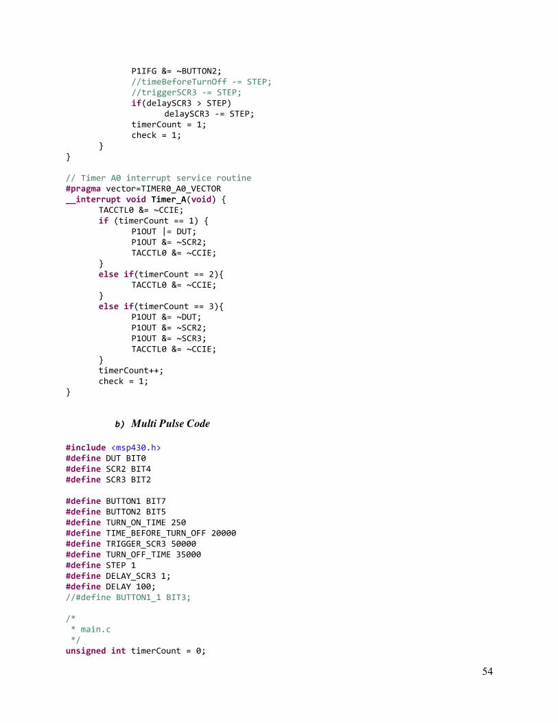
b) Multi Pulse Code
#include <msp430.h> #define DUT BIT0 #define SCR2 BIT4 #define SCR3 BIT2 #define BUTTON1 BIT7 #define BUTTON2 BIT5 #define TURN_ON_TIME 250 #define TIME_BEFORE_TURN_OFF 20000 #define TRIGGER_SCR3 50000 #define TURN_OFF_TIME 35000 #define STEP 1 #define DELAY_SCR3 1; #define DELAY 100; //#define BUTTON1_1 BIT3; /* * main.c */ unsigned int timerCount = 0;
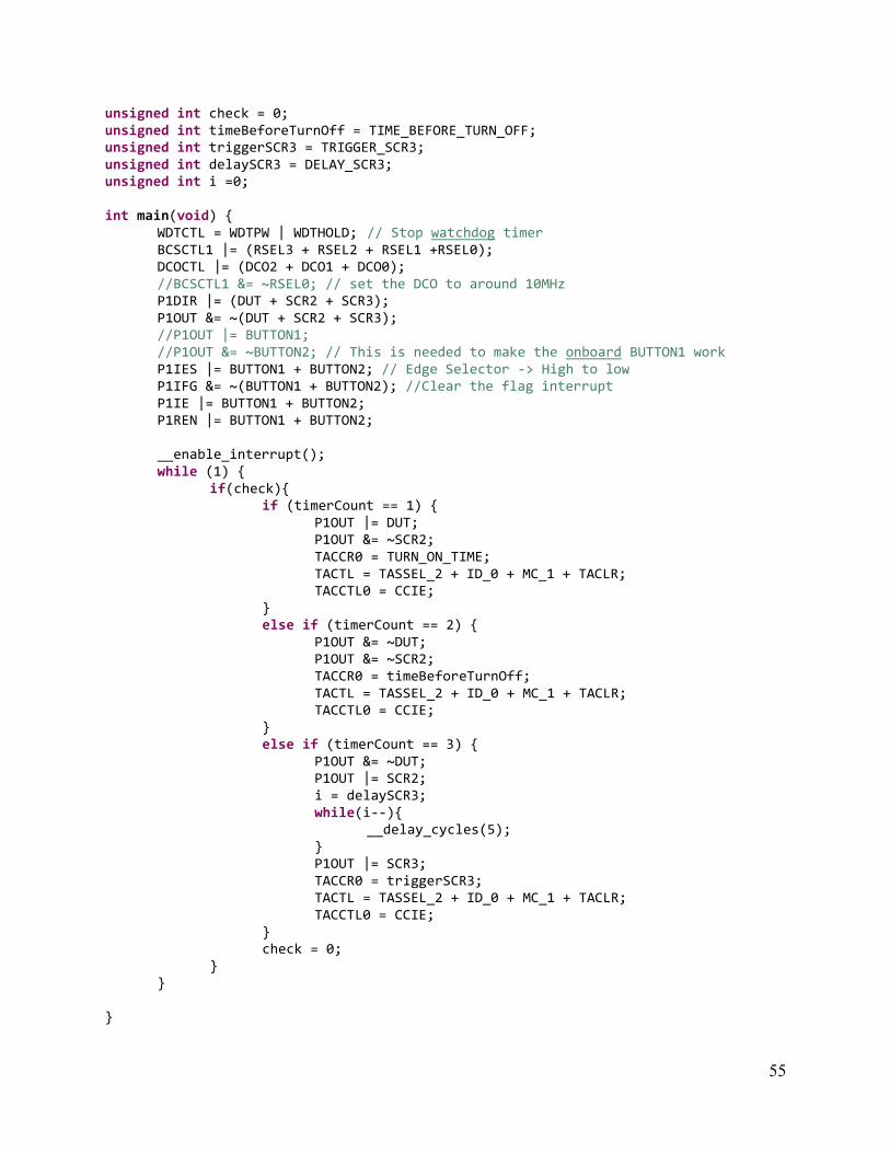
55
unsigned int check = 0; unsigned int timeBeforeTurnOff = TIME_BEFORE_TURN_OFF; unsigned int triggerSCR3 = TRIGGER_SCR3; unsigned int delaySCR3 = DELAY_SCR3; unsigned int i =0; int main(void) { WDTCTL = WDTPW | WDTHOLD; // Stop watchdog timer BCSCTL1 |= (RSEL3 + RSEL2 + RSEL1 +RSEL0); DCOCTL |= (DCO2 + DCO1 + DCO0); //BCSCTL1 &= ~RSEL0; // set the DCO to around 10MHz P1DIR |= (DUT + SCR2 + SCR3); P1OUT &= ~(DUT + SCR2 + SCR3); //P1OUT |= BUTTON1; //P1OUT &= ~BUTTON2; // This is needed to make the onboard BUTTON1 work P1IES |= BUTTON1 + BUTTON2; // Edge Selector -> High to low P1IFG &= ~(BUTTON1 + BUTTON2); //Clear the flag interrupt P1IE |= BUTTON1 + BUTTON2; P1REN |= BUTTON1 + BUTTON2; __enable_interrupt(); while (1) { if(check){ if (timerCount == 1) { P1OUT |= DUT; P1OUT &= ~SCR2; TACCR0 = TURN_ON_TIME; TACTL = TASSEL_2 + ID_0 + MC_1 + TACLR; TACCTL0 = CCIE; } else if (timerCount == 2) { P1OUT &= ~DUT; P1OUT &= ~SCR2; TACCR0 = timeBeforeTurnOff; TACTL = TASSEL_2 + ID_0 + MC_1 + TACLR; TACCTL0 = CCIE; } else if (timerCount == 3) { P1OUT &= ~DUT; P1OUT |= SCR2; i = delaySCR3; while(i--){ __delay_cycles(5); } P1OUT |= SCR3; TACCR0 = triggerSCR3; TACTL = TASSEL_2 + ID_0 + MC_1 + TACLR; TACCTL0 = CCIE; } check = 0; } } }
56
#pragma vector=PORT1_VECTOR __interrupt void Port_1(void) { if(P1IFG & BUTTON1){ P1IFG &= ~BUTTON1; //timeBeforeTurnOff += STEP; //triggerSCR3 += STEP; if(delaySCR3 <65000) delaySCR3 += STEP; timerCount = 1; check = 1; } else if(P1IFG & BUTTON2){ P1IFG &= ~BUTTON2; //timeBeforeTurnOff -= STEP; //triggerSCR3 -= STEP; if(delaySCR3 > STEP) delaySCR3 -= STEP; timerCount = 1; check = 1; } } // Timer A0 interrupt service routine #pragma vector=TIMER0_A0_VECTOR __interrupt void Timer_A(void) { TACCTL0 &= ~CCIE; if (timerCount == 1) { P1OUT &= ~DUT; P1OUT &= ~SCR2; TACCTL0 &= ~CCIE; } else if(timerCount == 2){ TACCTL0 &= ~CCIE; } else if(timerCount == 3){ P1OUT &= ~DUT; P1OUT &= ~SCR2; P1OUT &= ~SCR3; TACCTL0 &= ~CCIE; } timerCount++; check = 1; }
57
References
“Thyristor Theory and Design Considerations.” ON Semiconductor. n.p, Nov. 2006. Web. 01
Aug. 2013. <http://www.onsemi.com/pub_link/Collateral/HBD855-D.PDF>
“Parameter list for SCRs, TRIACs, AC switches, and DIACS.” ST Electronics. n.p, March 2008.
Web. 15 Jun. 2013.<http://www.st.com/st-web-
ui/static/active/en/resource/technical/document/application_note/CD00183570.pdf>
“Commutation of Thyristor-Based Circuits Part-I.” Indian Institute of Technology. n.p, n.d. Web.
09 Jun. 2013. <http://www.nptel.iitm.ac.in/courses/Webcourse-
contents/IIT%20Kharagpur/Power%20Electronics/PDF/L-
19(SSG)(PE)%20((EE)NPTEL)%20.pdf>