trends in mmwave devices, ics and packaging for ... · 55,000 process steps completed per mo . ......
TRANSCRIPT

Trends in mmWave devices, ICs and packaging for electronics test and measurement
Daniel Thomasson, PhD Director, Keysight HFTC
October 2014

Trends in mmWave devices, ICs & packaging for electronics T&M
– Keysight & HFTC Intro
– Market Drivers
– Technology Needs
– IC
– Device Technology
– Packaging
– Summary
UC Davis DMRC

Introduction to Keysight & HFTC
UC Davis DMRC

A Brief History of Keysight
1939–1998: The Hewlett-Packard years A company founded on electronic measurement innovation
1999–2013: The Agilent Technologies years Spun off from HP, Agilent became the World’s Premier Measurement Company In September 2013, announced the spin off its electronic measurement business
2014: Keysight begins operations Focused 100% on electronic measurement industry

Market Leadership in Core Platforms
Core Platforms Leadership Position
Electronic Design Automation
Highest performance design software used by 2/3 of the world’s RF/Microwave designers
Network Analyzers
Highest performance, broadest offering, including industry-leading PNA-X microwave network analyzers
Signal Analyzers
Highest performance signal analyzer family, including the flagship PXA X-Series
Signal Sources
Highest performance signal generators led by the industry-standard PSG performance signal generator
Oscilloscopes Product leadership in high-performance oscilloscopes via proprietary technology and application expertise
One Box Testers Two new R&D (UXM) and manufacturing (EXM) platforms for 4G and beyond

Technology for Electronics Measurement
>20 dB Better …than what our customers need to measure
Broadband Frequency Coverage
High Dynamic Range High Power & Low Noise Floor
High Fidelity / Low Distortion Mod Quality/EVM/Spurs/Harmonics
Low Noise Amplitude & Phase Noise
High Repeatability
Robust Manufacturability
High Reliability
Low Cost of Ownership
Long Platform Life
High Mix – Low Volume

Leading Edge
T&M Grade Manufacturing
Performance • Value • Quality

Invent and deliver world-leading signal conditioning technology
HFTC University Access Tech Access
High Frequency Technology Center
Basic Research Development Design NPI Mfg Applied
Research
High-Performance GaAs • InP • >200 GHz transistors • THz diodes World-class R&D and manufacturing engineers
75 professionals • 30 PhDs • 140 production
High-Mix 13 core technologies
200+ IC products
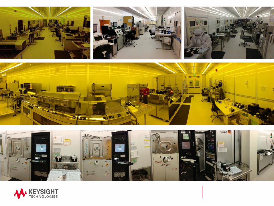
High-Complexity Low-Volume 55,000 process steps completed per mo
555 process steps per wafer 2500 wafers • 3M chips/yr
High-Quality
4000 ft2 Reliability Lab 100% dc/rf KGD

Design & Development
Pilot & Production
R&D & Production Rel
Photo removed

HFTC mmWave Enabling the 90000 Q-series 63 GHz Oscilloscope
Innovative Technology… • mmWave InP HBT, PHEMT and Schottky MMICs and Diodes
• Precision Hybrid Microcircuit solutions deliver 63 GHz
• Innovative architecture
Enables Differentiation… • Industry’s highest real time bandwidth - 63 GHz on two channels
• Industry’s highest 4-channel bandwidth - 33 GHz, 160 GS/s
• Industry’s lowest noise and jitter measurement floor
• Industry’s deepest memory - 2 Gpts
… in the World’s Most Accurate Real time Oscilloscope
Acquisition Board
mmWave Chipset
63 GHz Microcircuits

Enabling Leading Products EXG and MXG
Signal Generators MCD
golden transmitter
in R&D
Infiniium 90000 X-Series Oscilloscope OPD
G-Rex InP chipset
highest bandwidth best signal fidelity
FieldFox Handheld Analyzer CTD
world’s highest
performance handheld
N9030A PXA Signal Analyzer MCD
flagship lead in
dynamic range & phase noise
Infiniium 9000 Series Oscilloscope OPD
superior reliability
excellent signal fidelity
PNA-X Network Analyzer CTD
303 MMICs, 31 designs
widest range of single-connection
measurements
E6607A EXT Wireless Comms. Test Set MCD
performance and speed
across multiple radio standards
86100D Infiniium DCA-X Oscilloscope OPD
Chameleon InP chipset
comprehensive jitter analysis
N9403B J-BERT Serial BERT ETD
industry’s best pulse fidelity

Market Drivers for mmWave in T&M
UC Davis DMRC

Millimeter-Wave Test & Measurement Market two broad segments
Aerospace & Defense
traditional frequency-domain (FD) drivers
Digital Communications
new time-domain (TD) drivers
UC Davis DMRC

Global Internet Traffic users access rates & methods services
http://www.ieee802.org/3/ad_hoc/bwa/BWA_Report.pdf
UC Davis DMRC

The Next Ten Years
– Today’s reality: immediate availability of data, always and everywhere
• fixed and mobile computing devices with high data bandwidth
• cloud storage with large-capacity data centers, network access
• broadband wired and wireless networks
– Tomorrow’s vision: the interconnection of people and things
• but both people and machines create and consume data
• the ‘the internet of things’ (IoT)
UC Davis DMRC

Ethernet the next ten years: 100Gbaud for 1TbE
adapted from http://www.ieee802.org/3/ad_hoc/bwa/BWA_Report.pdf, “The need for speed: beyond 100GbE,” OFC 2013 Panel #2, and http://www.nanog.org/meetings/nanog52/presentations/Tuesday/hankins-100-gbe-and-beyond.pdf
Major challenges: • technical: baud rate, channel
density and power/bit • economic: cost/bit • market: hit the window
• represents a very strong future TD driver
• TD instruments must keep up to support new standards
UC Davis DMRC

Mobile
– revolutionary, not evolutionary
• speed: 10Gb/s, 100× faster than 4G
• latency: 1ms for M2M and IoT
• mobility: available everywhere
• density: very crowded
• low cost, low energy
– safe assumptions
• microwave & mmWave frequencies: 10-50, 60, 70-80GHz, …
• wide bandwidths: 500MHz to 3GHz
• new antenna technologies: steerable arrays, massive MIMO
the next ten years: 5G is mmWave cellular
Gerhard P. Fettweis, ”5G – what will it be: the tactile internet,” IEEE ICC, Jun 2013. A. Osseiran, “Mobile and wireless communications system for 2020 and beyond (5G),” ITU-R 2020 Vision Workshop, 12 Feb 2014, available at https://www.metis2020.com/documents/presentations/.
5G
2020
today
today
UC Davis DMRC

1
10
100
1000
1960 1970 1980 1990 2000 2010 2020
Ban
dw
idth
(G
Hz)
Year of Introduction
Broadband Instrument Bandwidth
VNA SA RT scope FD trend TD trend
The Result…
frequency domain VNA and SA
2× every ~15yr
time-domain real-time oscilloscope
2× every ~3yr
UC Davis DMRC

T&M Technology Needs
UC Davis DMRC

CMOS Performance and Density Continue to Advance
CMOS mm-wave research/product development on-going
From: http://www.digitaltonto.com/2011/4-digital-laws/
CMOS – Impressive Achievements
UC Davis DMRC

CMOS – 70-85 GHz Example
UC Davis DMRC

CMOS not the T&M solution …
Limited Voltage Swing Limited Dynamic Range
Limited Linearity Very limited BB power
0
1
2
3
4
5
6
1980 1990 2000 2010 2020
Logi
c Le
vel (
Vo
lts)
Logic Levels
Logic Levels
Break Down Voltages drop as Ft & Fmax Increase Limits Dynamic Range and Broad-Band Power
CMOS – Analog Limitations
UC Davis DMRC

T&M Requirements
Challenges Broad Bandwidths DC – 110+ GHz
High Dynamic Range -130dBm to +30dBm Extreme Linearity 50 dBm TOI, 75 to 90dBc ACPR Low Spurious, Low Harmonics, Low Phase Noise
PXI and Handheld-Specific Challenges DC Power Dissipation
Costs Size
Source Block Diagram Spectrum Analyzer Block Diagram
UC Davis DMRC

Challenges to Integration
Optimum Technology Differs by Functional Block • CMOS – digital • GaN – power • HBTs – gain, complex analog • YIGs, Cavities, etc. - Filters • etc.
80dBc ACPR 130dB Isolation
100dB Isolation 10MHz – 110GHz 20Vpp Swings
90+dBc ACPR 45 - 55 dBm TOI
90dBc Spurs
3Hz – 110GHz 20Vpp Swings
70dB Isolation
Very High Drive Very High TOI
Low Loss Switches
Low Noise Amps
Isolation • Chip Isolation Decreases with Frequency • ~40dB typical 30GHz • Often need >100 dB
Performance Expectations • Broadband, 50 ohm Equipment • 30 dBm Power Handling, 20Vpp • Better Performance than DUT - commercial system ~40dBc ACPR - test system ~75dBc ACPR
UC Davis DMRC

IC Trends
UC Davis DMRC

Page
IQ Modulators
Detectors
Shocklines & 3 Samplers
Switches & Attenuators
Digital MMICs
Amplifiers
Limiters
MMIC Portfolio >200 IC products covering DC to >100GHz
Mixers & Multipliers
UC Davis DMRC

Page
Trends for mmW T&M ICs
Top Drivers – frequency (bandwidth)
– spectral efficiency (bit/Hz)
– cost (economics)
• higher levels of integration
• lower cost of test
mmW T&M IC Trends
– fast transistors
– multiple semi technologies
– analog, digital & microwave design techniques in same IC
UC Davis DMRC

Page
Single-Ended Amplifiers
29
broadband and banded topologies
UC Davis DMRC

Page
Broadband Differential Amplifiers
30
limiting and linear topologies
UC Davis DMRC

Page
Mixed-Signal ICs
31
money-specs = analog characteristics of digital signal
UC Davis DMRC

Mixed-Signal ICs coming soon: fully distributed mixed-signal ICs
wavelength at 120GHz ~ 1mm
min length of a distributed element
flip-flop
amplifier
mixer
amplifier
wavelength at 30GHz ~ 4mm
min length of a distributed element
distributed design
lumped design
• IC design methodology changes dramatically when the physical element sizes > 10% of a wavelength • future mixed-signal ICs designed to operate at the fastest data rates will cross this threshold, becoming
‘distributed’ mixed-signal ICs, a term usually reserved for amplifiers
UC Davis DMRC

Device Technology Trends
UC Davis DMRC
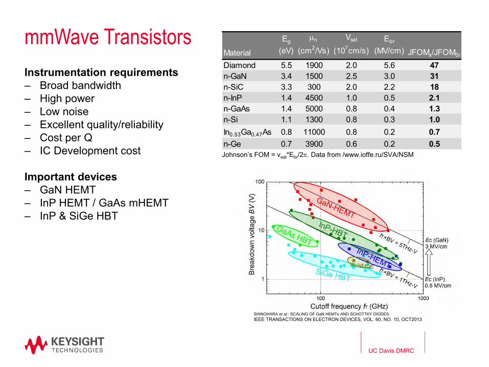
mmWave Transistors
Instrumentation requirements ‒ Broad bandwidth ‒ High power ‒ Low noise ‒ Excellent quality/reliability ‒ Cost per Q ‒ IC Development cost
Important devices ‒ GaN HEMT ‒ InP HEMT / GaAs mHEMT ‒ InP & SiGe HBT
SHINOHARA et al.: SCALING OF GaN HEMTs AND SCHOTTKY DIODES IEEE TRANSACTIONS ON ELECTRON DEVICES, VOL. 60, NO. 10, OCT2013
Johnson’s FOM = vsat*Ebr/2p. Data from /www.ioffe.ru/SVA/NSM
Material
Eg
(eV)
mn
(cm2/Vs)
Vsat
(107cm/s)Ebr
(MV/cm) JFOMx/JFOMSi
Diamond 5.5 1900 2.0 5.6 47n-GaN 3.4 1500 2.5 3.0 31n-SiC 3.3 300 2.0 2.2 18n-InP 1.4 4500 1.0 0.5 2.1n-GaAs 1.4 5000 0.8 0.4 1.3n-Si 1.1 1300 0.8 0.3 1.0In0.53Ga0.47As 0.8 11000 0.8 0.2 0.7n-Ge 0.7 3900 0.6 0.2 0.5
UC Davis DMRC

GaN HEMT
Intrinsically Advantageous Material System ‒ Wide bandgap, large BV → high power ‒ 2DEG density 5-10X higher than other III-V ‒ High electron mobility and saturated velocity ‒ Many strong GaN programs
HRL 70-110GHz GaN-based PA – from “WPA” datasheet
Promise ‒ Ft, Fmax > 300 GHz (production quality) ‒ IC bandwidth > 200GHz (production quality)
Challenges Trap related effects! ‒ Instrument level quality and reliability ‒ Instrument level noise, linearity, signal integrity ‒ Integration for 1000Q ICs ‒ Modeling and design infrastructure ‒ T&M needs a Watt with fantastic signal integrity and
stability more than 10 Watts with compromised SI
Pout = 18 dBm
SHINOHARA et al. IEDM2011 pp. 19.1.1
Expect to be significant for targeted T&M applications
UC Davis DMRC

GaAs mHEMT / InP HEMT Status
Very high frequency, not much breakdown ‒ InGaAs 2DEG has high electron mobility ‒ BV and power limit by narrow InGaAs bandgap ‒ Few players Promise ‒ Scaling of gates to < 50 nm
‒ Ft, Fmax > 1 THz ‒ IC bandwidth > 400 GHZ
Challenges
− Power slump at moderate drain voltages − Low integration limits functionality
Niche player getting pressed by other technologies. Wins at very highest frequencies
UC Davis DMRC

SiGe HBTs
− Benefits: fast, high integration→ order(s) magnitude more transistors than III-V − Challenges: low breakdown voltage, high NRE mask costs relative to low vol T&M − SiGe makes sense in many applications and we design in it when volumes justify
Ruker et al, SiRF 2012 pp133 Technology for highest integration, when low voltage ok, high volumes
UC Davis DMRC

InP HBTs
Benefits – Much higher breakdown voltage than SiGe HBTs
→ Higher output voltage/power – Very high speed (heading to THz) – Higher integration levels versus HEMTs – Much lower development cost as internal foundry
Future Direction – higher integration, faster
Xu, CSICS, 2014
Lobisser, IPRM, 2012
High performance and broad applicability to T&M.
UC Davis DMRC

T&M mmWave Device Summary
Technology Future
Mature GaAs Fully meets many needs. Cheap. Important for long time to come.
GaN Significant for targeted BB power applications, especially where GaAs has reached limits.
InP HEMT/mHEMT Niche player. Ultra-high frequency only.
SiGe HBT Many applications. Fast & high integration, but low breakdown and more costly for high mix-low-vol.
InP HBTs Fast & high breakdown w/ moderate integration. Many applications now. Workhorse.
UC Davis DMRC

mmW Packaging
UC Davis DMRC

(#) New MMIC/QFN, R=recent release ramp
T&M Packaging Technologies
Key Attributes • Reliability (environmental)
• Performance (loss/isolation/match)
• ‘Right sized’ for the application (cost/size)
• Support ICs (CTE/thermal/bias/mechanical)
Drivers • Increased IC power dissipation
• Increased IC functionality – I/O count
• Higher frequency
• Higher density
From 2-port, 1-source
To 4-port, 2-sources 26-50-67GHz
PXI format Up to 32-port 26 GHz VNA per mainframe
Handheld No-vents, battery powered 26GHz VNA, SA, power meter
UC Davis DMRC

Tota
l S
olu
tion C
ost
Performance (freq, integration, isolation, power handling etc.)
SMT
Hybrid
In PCB
Hybrid
SMT
Hybrid on
PCB
Hybrid uckt
Packaging Value Model
UC Davis DMRC

SMT
• Flexibility in layout and integration
• On-going push for high speed PCBs
• QFN (Quad Flat-pack Non-leaded) • Plastic encapsulated • Industry standard • Flexible sizes • Minimize lead inductance • Microwave performance
Mold Compound Die
Cu Leadframe Gold Wire
Lands
QFN section
High Density PCA
microwave performance at
PCB cost
UC Davis DMRC

Hybrid
• Traditional – proven microcircuit technology
• Performance to 110GHz and beyond
• Optimal thermal environment
• Hermetic possible
• Supports 3D designs
mmWave & sub-mmWave premium solution
UC Davis DMRC

Summary
UC Davis DMRC
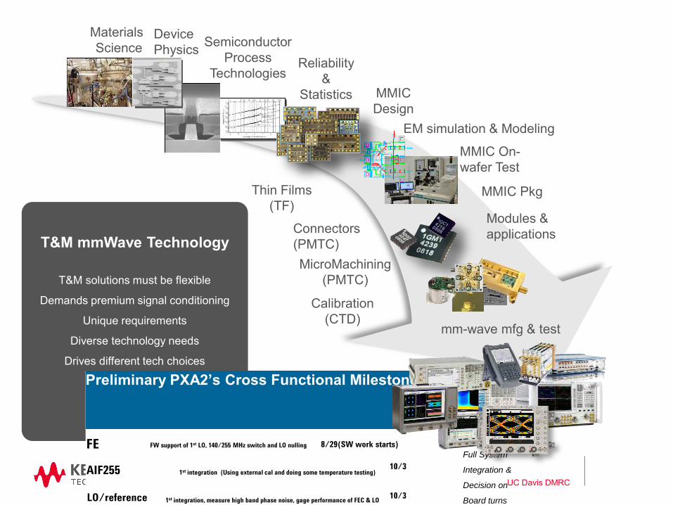
Materials Science
Device Physics Semiconductor
Process Technologies
Reliability &
Statistics MMIC Design
MMIC Pkg
MMIC On-wafer Test
Modules & applications
Thin Films (TF)
Connectors (PMTC) MicroMachining
(PMTC)
T&M mmWave Technology
T&M solutions must be flexible
Demands premium signal conditioning
Unique requirements
Diverse technology needs
Drives different tech choices
Exciting challenges
Many opportunities
Calibration (CTD)
EM simulation & Modeling
mm-wave mfg & test
Preliminary PXA2’s Cross Functional Milestones
Agilent Private
March-2011Page 7
FE FW support of 1st LO, 140/255 MHz switch and LO nulling 8/29(SW work starts)
AIF255 1st integration (Using external cal and doing some temperature testing)10/3
LO/reference 1st integration, measure high band phase noise, gage performance of FEC & LO10/3
RTSA White paper due 10/31
FFT sweep speed up
Chirp sweep Bench mark FFT engine with SW optimization
1st report (7/25) 2nd report (10/31)
Partial re-config.?(7/25)
NPI SHC model (7/11) Specs(7/18) Roll out options(7/25) EI test equipments(9/5) New SCPI defined (9/26)
Full System
Integration &
Decision on
Board turns
11/21/2011
8/8
DEF 10/14
TR2 10/11
RTSA PD work starts
RTSA implementation & proof
Of concept
PCIe To PCD 6/27 To FAB 7/18 Board turned on 8/29 FW defined 9/18 Fully tested 10/14
<CON>
<INV> <DEF>
UC Davis DMRC