tp801 pci hardware manual - tiepie - usb...
TRANSCRIPT
User Manual
TP801 PCI
a multifunctional PC measuring instrument
TiePie engineering

Despite the care taken for the compilation of this book, TiePie eng-ineering can not be held responsible for any damages resulting fromerrors that may appear in this book.
All rights reserved. No part of this book may be reproduced, stored in adatabase or retrieval system, or published, in any form or in any way,electronically, mechanically, by print, photoprint, microfilm or any othermeans without prior written permission from TiePie engineering.
User Manual
TP801 PCI
a multifunctional PC measuring instrument
TiePie engineering

Contents i
Contents
Declaration of Confirmity . . . . . . . . . . . . . . . . . . . . . . . . . . . . 3
Introduction . . . . . . . . . . . . . . . . . . . . . . . . . . . . . . . . . . . . . . 5Sampling . . . . . . . . . . . . . . . . . . . . . . . . . . . . . . . . . . . . . . . . 5- Aliasing . . . . . . . . . . . . . . . . . . . . . . . . . . . . . . . . . . . . . . . 6Digitising . . . . . . . . . . . . . . . . . . . . . . . . . . . . . . . . . . . . . . . . 7The measuring system of the TP801 PCI . . . . . . . . . . . . . . . . . 8The probes . . . . . . . . . . . . . . . . . . . . . . . . . . . . . . . . . . . . . . 8
Safety . . . . . . . . . . . . . . . . . . . . . . . . . . . . . . . . . . . . . . . . . 11
Hardware installation . . . . . . . . . . . . . . . . . . . . . . . . . . . . . 13
Driver installation . . . . . . . . . . . . . . . . . . . . . . . . . . . . . . . . 15Step 1 . . . . . . . . . . . . . . . . . . . . . . . . . . . . . . . . . . . . . . . . 15Step 2 . . . . . . . . . . . . . . . . . . . . . . . . . . . . . . . . . . . . . . . . 16Step 3 . . . . . . . . . . . . . . . . . . . . . . . . . . . . . . . . . . . . . . . . 17Step 4 . . . . . . . . . . . . . . . . . . . . . . . . . . . . . . . . . . . . . . . . 18Step 5 . . . . . . . . . . . . . . . . . . . . . . . . . . . . . . . . . . . . . . . . 19
Technical information . . . . . . . . . . . . . . . . . . . . . . . . . . . . . 21Pin assignments of the connectors . . . . . . . . . . . . . . . . . . . . . 21- 16 pin header (J2) . . . . . . . . . . . . . . . . . . . . . . . . . . . . . . 21External 15 pin sub-D connector . . . . . . . . . . . . . . . . . . . . . 22BNC connectors . . . . . . . . . . . . . . . . . . . . . . . . . . . . . . . . . 22
Specifications . . . . . . . . . . . . . . . . . . . . . . . . . . . . . . . . . . . 23A/D converter . . . . . . . . . . . . . . . . . . . . . . . . . . . . . . . . . . . 23Analog input BNC . . . . . . . . . . . . . . . . . . . . . . . . . . . . . . . . 23Digital external trigger . . . . . . . . . . . . . . . . . . . . . . . . . . . . . 23Arbitrary Waveform Generator . . . . . . . . . . . . . . . . . . . . . . 23Trigger system . . . . . . . . . . . . . . . . . . . . . . . . . . . . . . . . . . 24Maximum sample rate . . . . . . . . . . . . . . . . . . . . . . . . . . . . . 24Memory . . . . . . . . . . . . . . . . . . . . . . . . . . . . . . . . . . . . . . . 24General . . . . . . . . . . . . . . . . . . . . . . . . . . . . . . . . . . . . . . . 24

ii

Declaration of Confirmity 3
TiePie engineeringKoperslagersstraat 378601 WL SneekNederland
EG-verklaring van overeenstemming
Wij verklaren geheel onder eigen verantwoordelijkheid, dathet produkt
TP801 PCI
waarop deze verklaring betrekking heeft, in overeenstemmingis met de geharmoniseerde Europese normen
EN55011, EN55022, EN50081-1 en EN50082-1
Volgens de bepalingen van de EMC-richtlijn 89/336/EEG,gewijzigd door de richtlijn 92/31/EEG en 93/68/EEG
Sneek, 12-5-2002 ir. A.P.W.M. Poelsma
TiePie engineeringKoperslagersstraat 378601 WL SneekThe Netherlands
EC declaration of Confirmity
We declare, on our own responsibility, that the product
TP801 PCI
for which this declaration is valid, is in compliance with
EN55011, EN55022, EN50081-1 and EN50082-1
according the conditions of the EMC standard 89/336/EEG,and the amendments 92/31/EEC and 93/68/EEC
Sneek, 12-5-2002 ir. A.P.W.M. Poelsma
TiePie engineeringKoperslagersstraat 378601 WL SneekThe Netherlands
EG - Konformitätserklärung
Wir erklären, in Eigenverantwortlichkeit, hiermit, daß das Pro-dukt
TP801 PCI
für das diese Erklärung gültig ist, mit
EN55011, EN55022, EN50081-1 und EN50082-1,
gemäß den Anforderungen des EMC-standards 89/336/EEC,und den Zusatzbestimmungen 92/31/EEC und 93/68/EECübereinstimmt.
Sneek, 12-5-2002 ir. A.P.W.M. Poelsma
TiePie engineeringKoperslagersstraat 378601 WL SneekThe Netherlands
Déclaration de conformité C.E.
Nous déclarons, sous notre responsibilité, que le produit
TP801 PCI
pour lequel cette déclaration est valide, est conforme aux:
EN55011, EN55022, EN50081-1 et EN50082-1
selon les conditions du standard CEM No 89/336/EEC, et lesamendements 92/31/EEC et 93/68/EEC
Sneek, 12-5-2002 ir. A.P.W.M. Poelsma
Declaration of Confirmity

4 Declaration of Confirmity
TiePie engineeringKoperslagersstraat 378601 WL SneekThe Netherlands
Dichiarazione di Conformita' CE
Dichiariamo sotto la nostra esclusiva responsabilitià che il pro-dotto:
TP801 PCI
per il quale vale la presente dichiarzione, è conforme alle nor-me
EN55011, EN55022, EN50081-1 e EN50082-1
conformente alle condizioni della normativa EMC89/336/EEC, e successive modifiche 92/31/EEC e93/68/EEC.
Sneek, 12-5-2002 ir. A.P.W.M. Poelsma
TiePie engineeringKoperslagersstraat 378601 WL SneekThe Netherlands
EC-declaración de conformidad
Nosotros declaramos, bajo nuestra propia responsabilidad,que el producto
TP801 PCI
para el cual esta declaración es válida, está en relación con
EN55011, EN55022, EN50081-1 y EN50082-1
Según las condiciones del EMC estándar 89/336/EEC, y losmovimientos 92/31/EEC y 93/68/EEC
Sneek, 12-5-2002 ir. A.P.W.M. Poelsma
TiePie engineeringKoperslagersstraat 378601 WL SneekThe Netherlands
EC Hyväksyntäilmoitus
Velvollisuutenamme on ilmoittaa, että tuotteemme
TP801 PCI
jota tämä selvitys koskee, on huväksytty
EN55011, EN55022, EN50081-1 ja EN50082-1
EMC standardien 89/336/EEG, ja lisästandardien 92/31/EECja 93/68/EEC mukaisesti
Sneek, 12-5-2002 ir. A.P.W.M. Poelsma
TiePie engineeringKoperslagersstraat 378601 WL SneekThe Netherlands
EF-Overensstemmelseserklæring
Undertegnede erklærer herved, at følgende apparat overhol-der beskyttelseskravene i Rådets direktiv 89/336/EØF omelektromagnetisk kompatibilet (EMC).
Identification af apparat:Kategori: MåleinstrumentModel/type: TP801 PCI
Standarder der er anvendt som grundlag for erklæring, ellerhenvisning til den prøvningsrapport, der er udstedt af et be-myndiget laboratorium:
EN55011, EN55022, EN50081-1 og EN50082-1
CE-mærket angiver kun overensstemmelse med EMC-direk-tiv 89/336/EØF
Sneek, 12-5-2002 ir. A.P.W.M. Poelsma
Introduction 5
Chapter 1Introduction
NOTE Before using the TP801 PCI, first read chapter 2,about Safety.
Many technicians investigate electrical signals. Though the measurementmay not be electrical, the physical variable is often converted to an electri-cal signal, with a special transducer. Common transducers are acceler-ometers, pressure probes, current clamps and temperature probes. Theadvantages of converting the physical parameters to electrical signals arelarge, since several instruments for examining electrical signals are availa-ble.
The TP801 PCI is a 2 channel, 8 bits, 100 Msamples/sec interface card,which can, with the acompanying software, be used as a digital storageoscilloscope, a spectrum analyzer, a voltmeter or a transient recorder. Allinstruments measure by sampling the input signals, digitalize the values,process them, save them and display them.
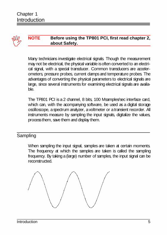
Sampling
When sampling the input signal, samples are taken at certain moments.The frequency at which the samples are taken is called the samplingfrequency. By taking a (large) number of samples, the input signal can bereconstructed.

6 Chapter 1
Tsample = 1 ms
Tapparent = 4 ms
Tin = 0.8 ms
In the latter illustration a sine wave signal is sampled with 50 samples. Byconnecting the adjacent samples, the original signal can be reconstructed.See also the next illustration.
The more samples are taken, the better the signal can be reconstructed.The sampling frequency must be higher than 2 times the highest frequen-cy in the input signal. This is called the Nyquist frequency. Theoretically itis possible to reconstruct the input signal with more than 2 samples. Inpractice, 10 to 20 samples are necessary to be able to examine the signalthoroughly.
Aliasing
If the sampling frequency is lower than 2 times the frequency of the inputsignal, 'aliasing' will occur. The following illustration shows how aliasingoccurs.
Introduction 7
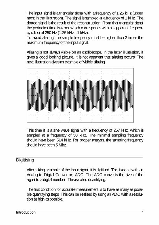
The input signal is a triangular signal with a frequency of 1.25 kHz (uppermost in the illustration). The signal is sampled at a frquency of 1 kHz. Thedotted signal is the result of the reconstruction. From that triangular signalthe periodical time is 4 ms, which corresponds with an apparent frequen-cy (alias) of 250 Hz (1.25 kHz - 1 kHz).To avoid aliasing, the sample frequency must be higher than 2 times themaximum frequency of the input signal.
Aliasing is not always visible on an oscilloscope. In the latter illustration, itgives a 'good looking' picture. It is not apparent that aliasing occurs. Thenext illustration gives an example of visible aliasing.
This time it is a sine wave signal with a frequency of 257 kHz, which issampled at a frequency of 50 kHz. The minimal sampling frequencyshould have been 514 kHz. For proper analysis, the sampling frequencyshould have been 5 Mhz.
Digitising
After taking a sample of the input signal, it is digitised. This is done with anAnalog to Digital Convertor, ADC. The ADC converts the size of thesignal to a digital number. This is called quantifying.
The first condition for accurate measurement is to have as many as possi-ble quantifying steps. This can be realised by using an ADC with a resolu-tion as high as possible.

8 Chapter 1
The resolution of ADC's is often given in bits. The number of bits deter-mines the number of quantifying steps according the formula:
number of quantifying steps = 2 number of bits
A 2 bits ADC has 4 quantifying steps. With an input range of 10 Volt, thisADC can divide the input range in 4 parts of each 2.5 Volt.
By increasing the number of bits, the resolution increases, the number ofquatifying steps increases and the sub-divisions get smaller.
The measuring system of the TP801 PCI
The TP801 PCI uses an 8 bits ADC with a maximum sampling frequencyof 50 MHz for each channel.
The TP801 PCI can sample 2 channels simultaneously with a maximumspeed of 50 million samples per second. By using a special technique, it isalso possible to measure one channel at a speed of 100 million samplesper second.
The two ADC's are switched to channel 1. One ADC starts sampling at50 MHz. The other ADC will also sample at 50 MHz, but at intervalsexactly between the moments the first ADC is sampling. By putting thesamples of both ADC's together, it is possible to sample a signal at 2 x 50MHz = 10 MHz. See also the next illustration.
This can only be done with channel 1 of the TP801 PCI.
Introduction 9
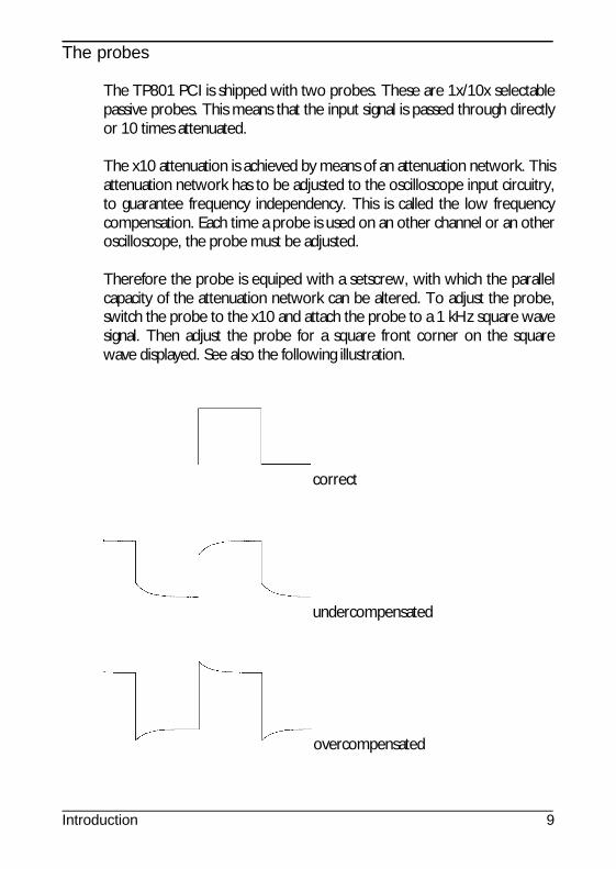
correct
undercompensated
overcompensated
The probes
The TP801 PCI is shipped with two probes. These are 1x/10x selectablepassive probes. This means that the input signal is passed through directlyor 10 times attenuated.
The x10 attenuation is achieved by means of an attenuation network. Thisattenuation network has to be adjusted to the oscilloscope input circuitry,to guarantee frequency independency. This is called the low frequencycompensation. Each time a probe is used on an other channel or an otheroscilloscope, the probe must be adjusted.
Therefore the probe is equiped with a setscrew, with which the parallelcapacity of the attenuation network can be altered. To adjust the probe,switch the probe to the x10 and attach the probe to a 1 kHz square wavesignal. Then adjust the probe for a square front corner on the squarewave displayed. See also the following illustration.

10 Chapter 1
Safety 11
Chapter 2Safety
Before you start working with the TP801 PCI, first read these safety rules.
C Avoid working alone.C Check the probes/testleads for damages. DO NOT use them if
they are damaged.C Take care when measuring voltages higher than 25 V AC or 60 V
DC.C The maximum input signal size is 200 V (DC + AC.peak < 10
kHz) Applying more than these voltages may damage your TP801PCI.
C Always choose the right function and range when measuring.C The TP801 PCI is grounded through the grounding conductor of
the power cord of the PC it is placed in. Plug the power cord in aproper, grounded outlet before making connections to the inputsand outputs of the TP801 PCI. Proper grounding is essential forsafe measuring.
C If the PC with the TP801 PCI is not grounded, all accessible con-ductive parts can render an electrical shock.

12 Chapter 2

Hardware installation 13
CH 1
CH 2
GENJ2
Chapter 3Hardware installation
The TP801 PCI is an interface card which can be placed in any free PCIslot of an IBM compatible AT. The card uses Plug and Play, so installationis quite simple.
Switch the power of your computer off, and remove the cables.
Before opening the computer and handling the card, be sure to removeany static electricity by touching a grounded metal part or wear a groun-ding strap.
Then open the computer and locate a free PCI slot. Remove the slotcover and insert tha TP801 PCI card. Then replace the cover of thecomputer, reconnect the cables and switch the power back on.

14 Chapter 3

Driver installation 15
Chapter 4Driver installation
After installing the TP801 PCI in the computer and powering up thecomputer, Windows will report that new hardware is found. Then it willstart the New Hardware wizard to install the driver for the TP801 PCI.
The following steps are required, the images show the operations toperform. The driver software is delivered on the CD that came with theTP801 PCI. In the images is assumed that the drive letter for theCDROM is D:.
Step 1

16 Chapter 4
Step 2

Driver installation 17
Step 3

18 Chapter 4
Step 4
Driver installation 19
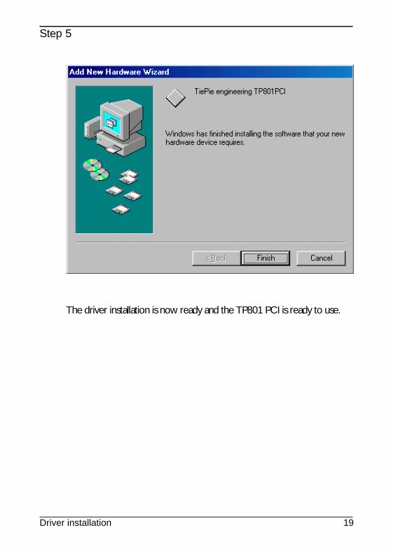
Step 5
The driver installation is now ready and the TP801 PCI is ready to use.

20 Chapter 4
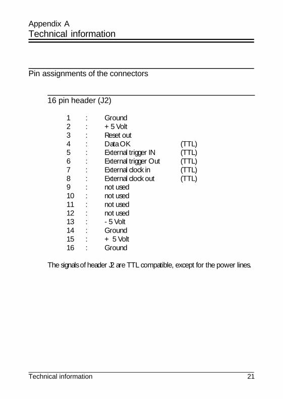
Technical information 21
Appendix ATechnical information
Pin assignments of the connectors
16 pin header (J2)
1 : Ground2 : +5 Volt3 : Reset out4 : Data OK (TTL)5 : External trigger IN (TTL)6 : External trigger Out (TTL)7 : External clock in (TTL)8 : External clock out (TTL)9 : not used10 : not used11 : not used12 : not used13 : - 5 Volt14 : Ground15 : + 5 Volt16 : Ground
The signals of header J2 are TTL compatible, except for the power lines.
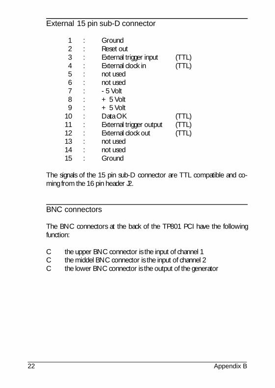
22 Appendix B
External 15 pin sub-D connector
1 : Ground 2 : Reset out 3 : External trigger input (TTL) 4 : External clock in (TTL) 5 : not used 6 : not used 7 : - 5 Volt 8 : + 5 Volt 9 : + 5 Volt10 : Data OK (TTL)11 : External trigger output (TTL)12 : External clock out (TTL)13 : not used14 : not used15 : Ground
The signals of the 15 pin sub-D connector are TTL compatible and co-ming from the 16 pin header J2.
BNC connectors
The BNC connectors at the back of the TP801 PCI have the followingfunction:
C the upper BNC connector is the input of channel 1C the middel BNC connector is the input of channel 2C the lower BNC connector is the output of the generator

Notes 23
Appendix BSpecifications
A/D converter
resolution 8 bits = 0.39%effective data throughput 50 000 000 samples/sec
100 000 000 samples/sec on one channelconversion time 20 nsec, 10 nsec on one channel
Analog input BNC
sensitivity 100 mvolt .. 80 volt full scalemaximum voltage 200 volt (DC + AC peak < 10 kHz)impedance 1 MS / 30 pFcoupling AC / DCaccuracy 1% ± 1 LSBbandwidth DC to 50 MhzSNR 7.3 bit / 43 dB
Digital external trigger
Levels 0 - 5 Volt TTL
Arbitrary Waveform Generator
sample rate 0 - 25 MHzresolution 10 bitbandwidth DC to 2 MHzimpedance 50 Ohmcoupling DCoutput amplitude -10 volt .. 10 voltamplitude step 0 - 10 V in 65535 steps, resolution 0.2 mVDC level 0 - 10 V in 65535 steps, resolution 0.2 mVWaveforms sine, triangle, square, DC, noise and user definedSymmetry 1 - 99%, 1% steps
24 Notes
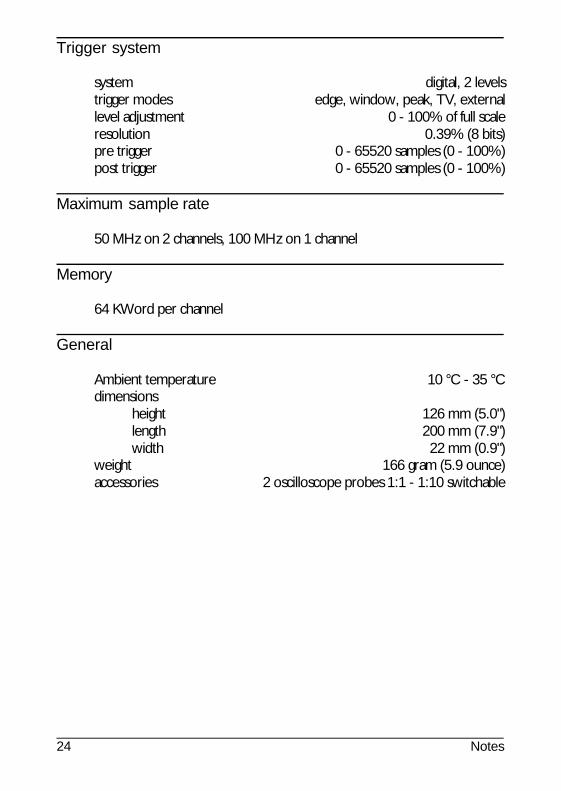
Trigger system
system digital, 2 levelstrigger modes edge, window, peak, TV, externallevel adjustment 0 - 100% of full scaleresolution 0.39% (8 bits)pre trigger 0 - 65520 samples (0 - 100%)post trigger 0 - 65520 samples (0 - 100%)
Maximum sample rate
50 MHz on 2 channels, 100 MHz on 1 channel
Memory
64 KWord per channel
General
Ambient temperature 10 °C - 35 °Cdimensions
height 126 mm (5.0")length 200 mm (7.9")width 22 mm (0.9")
weight 166 gram (5.9 ounce)accessories 2 oscilloscope probes 1:1 - 1:10 switchable

Notes 25
Notes

26 Notes

If you have any suggestions and/or remarks concerning the program, theTP801 PCI or the manual, please contact:
TiePie engineeringPO Box 2908600 AG SNEEK
Visitors address:
TiePie engineeringKoperslagersstraat 378601 WL SNEEKTel.: +31 515 415 416Fax: +31 515 418 819

TP801 PCI manual rev 1.0