topic: sequential circuits, latches and flip flops unit iv
TRANSCRIPT

Topic: Sequential Circuits, Latches and
Flip flopsUNIT IV:
Lecture No.: 26
1

Introduction to Sequential Circuits
Sequential circuits are those in which the output depends not only on the present inputs, but also on the previous output state and/or the previous inputs.
Prepared and Delivered By: Irfan Ahmad Pindoo 2
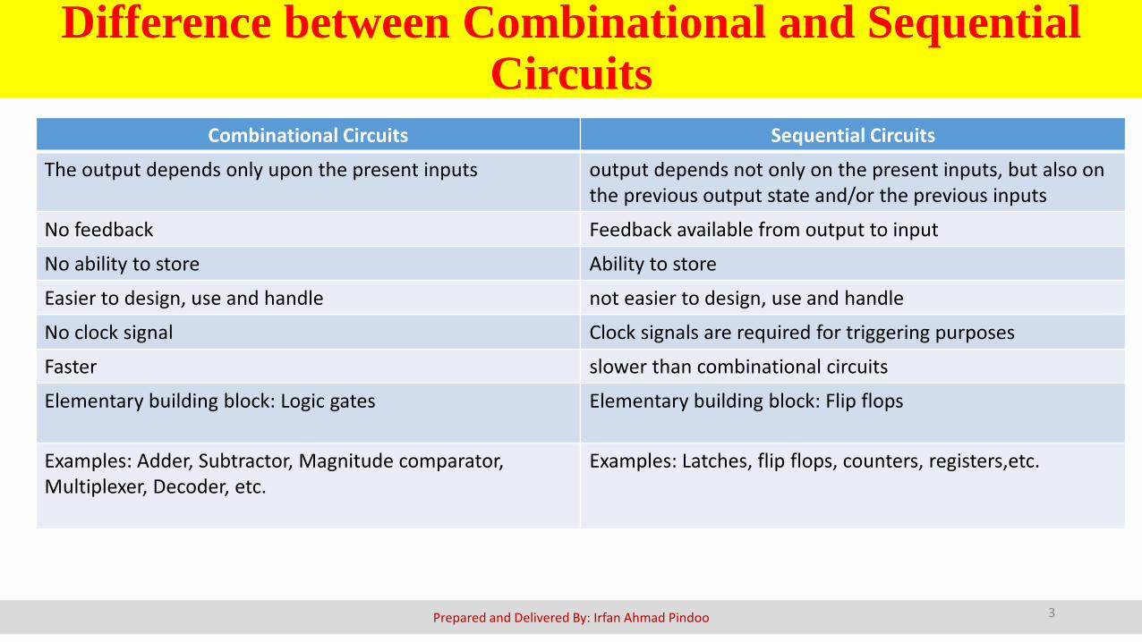
Difference between Combinational and Sequential Circuits
Combinational Circuits Sequential Circuits
The output depends only upon the present inputs output depends not only on the present inputs, but also on the previous output state and/or the previous inputs
No feedback Feedback available from output to input
No ability to store Ability to store
Easier to design, use and handle not easier to design, use and handle
No clock signal Clock signals are required for triggering purposes
Faster slower than combinational circuits
Elementary building block: Logic gates Elementary building block: Flip flops
Examples: Adder, Subtractor, Magnitude comparator, Multiplexer, Decoder, etc.
Examples: Latches, flip flops, counters, registers,etc.
Prepared and Delivered By: Irfan Ahmad Pindoo 3

Which of the following is NOT the combinational circuit?
a) magnitude comparator
b) multiplexer
c) parity generator circuit
d) Flip flop
4
QUICK QUIZ (POLL)
Prepared and Delivered By: Irfan Ahmad Pindoo
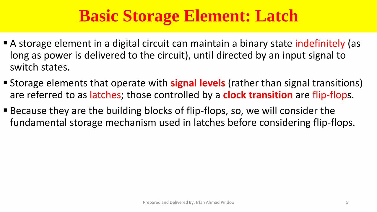
Basic Storage Element: Latch
A storage element in a digital circuit can maintain a binary state indefinitely (as long as power is delivered to the circuit), until directed by an input signal to switch states.
Storage elements that operate with signal levels (rather than signal transitions) are referred to as latches; those controlled by a clock transition are flip-flops.
Because they are the building blocks of flip-flops, so, we will consider the fundamental storage mechanism used in latches before considering flip-flops.
5Prepared and Delivered By: Irfan Ahmad Pindoo

SR Latch
The SR latch is a circuit with two cross-coupled NOR gates or two cross-coupled NAND gates, and two inputs labeled S for set and R for reset.
The latch has two useful states: 1. When output Q = 1 and 𝑄′= 0, the latch is said to be in the set state.
2. When Q = 0 and 𝑄′= 1, it is in the reset state.
Outputs Q and 𝑄′are normally the complement of each other. Otherwise, the device will enter an unpredictable or undefined state or a metastable state.
6Prepared and Delivered By: Irfan Ahmad Pindoo

What is the output state in SR latch at Q = 1 and 𝑄′= 0
a) set
b) reset
c) memory
d) indeterminate
Prepared and Delivered By: Irfan Ahmad Pindoo 7
QUICK QUIZ (POLL)

SR NOR Latch
Prepared and Delivered By: Irfan Ahmad Pindoo 8

Which of the following state is invalid/indeterminate in SR NOR latch?
a) S=1, R= 0
b) S=0, R= 1
c) S=0, R= 0
d) S=1, R= 1
Prepared and Delivered By: Irfan Ahmad Pindoo 9
QUICK QUIZ (POLL)

SR NAND Latch
Prepared and Delivered By: Irfan Ahmad Pindoo 10
•
𝑆′𝑅′•

Which of the following state is invalid/indeterminate in SR NAND latch?
a) S=1, R= 0
b) S=0, R= 1
c) S=0, R= 0
d) S=1, R= 1
Prepared and Delivered By: Irfan Ahmad Pindoo 11
QUICK QUIZ (POLL)

SR Latch with control input
The operation of the basic SR latch can be modified by providing an additionalinput signal that determines (controls) when the state of the latch can bechanged by determining whether S and R can affect the circuit.
Prepared and Delivered By: Irfan Ahmad Pindoo 13

What is the output state in SR enabled NAND based latch at S=1, R= 0, and En=0?
a) Q= set
b) Q=reset
c) Q=memory
d) Q=indeterminate
Prepared and Delivered By: Irfan Ahmad Pindoo 14
QUICK QUIZ (POLL)

D Latch (Transparent Latch)
One way to eliminate the undesirable condition of the indeterminate state inthe SR latch is to ensure that inputs S and R are never equal to 1 or 0 at thesame time. This is done in the D latch.
Prepared and Delivered By: Irfan Ahmad Pindoo 16

D Latch (Transparent Latch)
The D latch receives that name from its ability to hold data in its internalstorage. It is suited for use as a temporary storage.
The binary information present at the data input of the D latch is transferred tothe Q output when the enable input is asserted.
The output follows changes in the data input as long as the enable input isasserted. This situation provides a path from input D to the output, and for thisreason, the circuit is often called a transparent latch.
When the enable input signal is de-asserted, the binary information that waspresent at the data input at the time the transition occurred is retained (i.e.,stored) at the Q output until the enable input is asserted again.
Prepared and Delivered By: Irfan Ahmad Pindoo 17

In D flip-flop, D stands for _____________
a) Distant
b) Data
c) Desired
d) Delay
18
QUICK QUIZ (POLL)
Topic: Sequential Circuits, Latches and
Flip flopsUNIT IV:
Lecture No.: 27
1

Flip Flop
A flip flop is an electronic circuit with two stable states that can be used to storebinary data. The stored data can be changed by applying varying inputs.
Flip-flops and latches are fundamental building blocks of digital electronicssystems used in computers, communications, and many other types of systems.
Prepared and Delivered By: Irfan Ahmad Pindoo 2

Flip flops are:
a) Level sensitive
b) Positive edge triggered
c) Negative edge triggered
d) Both b and c
Prepared and Delivered By: Irfan Ahmad Pindoo 3
QUICK QUIZ (POLL)

Difference between Latch and Flip Flop
Latch Flip flop
Level sensitive Edge sensitive
A latch doesn’t contain any clock signal A flip-flop contains a clock signal
The structure of Latches is built with logic gates FFs are designed with latches by adding an extra clock signal.
Latches are responsive toward faults on enable pin FFs are protected toward faults
Asynchronous Synchronous
Faster Slower
Prepared and Delivered By: Irfan Ahmad Pindoo 4
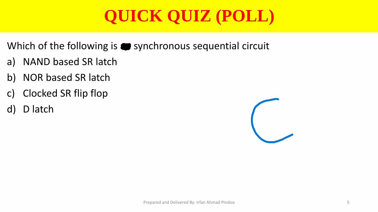
Which of the following is an synchronous sequential circuit
a) NAND based SR latch
b) NOR based SR latch
c) Clocked SR flip flop
d) D latch
Prepared and Delivered By: Irfan Ahmad Pindoo 5
QUICK QUIZ (POLL)

Types of Flip Flop
Prepared and Delivered By: Irfan Ahmad Pindoo 6
SR flip flop D flip flop
JK flip flop T flip flop

SR Flip Flop
Prepared and Delivered By: Irfan Ahmad Pindoo 7
CLK S R 𝑸𝒏 𝑸𝒏+𝟏 𝑸𝒏+𝟏
0 × × × 𝑸𝒏 𝑸𝒏
1 0 0 0
1 0 0 1
1 0 1 0
1 0 1 1
1 1 0 0
1 1 0 1
1 1 1 0
1 1 1 1
Characteristic Table:

SR Flip Flop
Prepared and Delivered By: Irfan Ahmad Pindoo 8
CLK S R 𝑸𝒏 𝑸𝒏+𝟏 𝑸𝒏+𝟏
0 × × × 𝑸𝒏 𝑸𝒏
1 0 0 0 0 1
1 0 0 1 1 0
1 0 1 0 0 1
1 0 1 1 0 1
1 1 0 0 1 0
1 1 0 1 1 0
1 1 1 0 Indeterminate
1 1 1 1 Indeterminate
Characteristic Table:
𝑹𝑸 𝑹𝑸 𝑹 𝑸 𝑹 𝑸
𝑺
𝑺

What would be the output state in clocked SR flip flop when S=1, R=0 and CLK=0?
a) SET
b) RESET
c) MEMORY
d) INVALID
Prepared and Delivered By: Irfan Ahmad Pindoo 9
QUICK QUIZ (POLL)
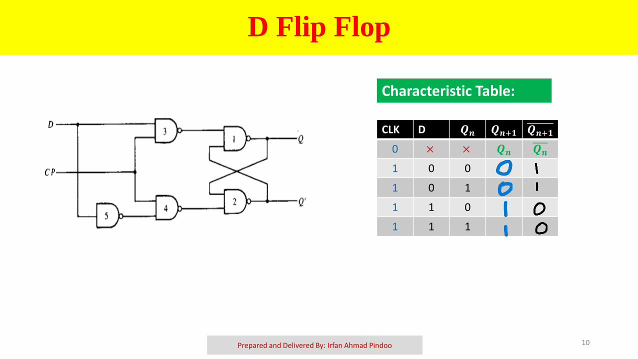
D Flip Flop
Prepared and Delivered By: Irfan Ahmad Pindoo 10
CLK D 𝑸𝒏 𝑸𝒏+𝟏 𝑸𝒏+𝟏
0 × × 𝑸𝒏 𝑸𝒏
1 0 0
1 0 1
1 1 0
1 1 1
Characteristic Table:
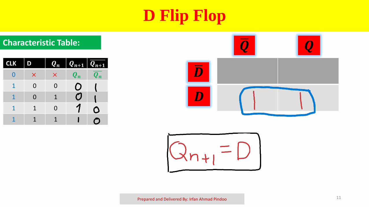
D Flip Flop
Prepared and Delivered By: Irfan Ahmad Pindoo 11
Characteristic Table:
CLK D 𝑸𝒏 𝑸𝒏+𝟏 𝑸𝒏+𝟏
0 × × 𝑸𝒏 𝑸𝒏
1 0 0
1 0 1
1 1 0
1 1 1
𝑫
𝑫
𝑸 𝑸

“The output is same as that of input, when clock is enabled”. This statement is true for
a) SR flip flop
b) D flip flop
c) JK flip flop
d) T flip flop
Prepared and Delivered By: Irfan Ahmad Pindoo 12
QUICK QUIZ (POLL)

Topic: Flip Flops and Race Around
ConditionUNIT IV:
Lecture No.: 28
1

JK Flip Flop
Prepared and Delivered By: Irfan Ahmad Pindoo 2
Characteristic Table:
CLK J K 𝑸𝒏 𝑸𝒏+𝟏 𝑸𝒏+𝟏
0 × × ×
1 0 0 0
1 0 0 1
1 0 1 0
1 0 1 1
1 1 0 0
1 1 0 1
1 1 1 0
1 1 1 1

JK Flip Flop
Prepared and Delivered By: Irfan Ahmad Pindoo 3
Characteristic Table:
𝑲𝑸 𝑲𝑸 𝑲 𝑸 𝑲 𝑸
𝑱
𝑱
CLK J K 𝑸𝒏 𝑸𝒏+𝟏 𝑸𝒏+𝟏
0 × × × 𝑸𝒏 𝑸𝒏
1 0 0 0 0 1
1 0 0 1 1 0
1 0 1 0 0 1
1 0 1 1 0 1
1 1 0 0 1 0
1 1 0 1 1 0
1 1 1 0 1 0
1 1 1 1 0 1

What would be the output state in clocked JK flip flop when J=1, K=1 and CLK=1?
a) SET
b) RESET
c) MEMORY
d) TOGGLE
Prepared and Delivered By: Irfan Ahmad Pindoo 4
QUICK QUIZ (POLL)

T Flip Flop
Prepared and Delivered By: Irfan Ahmad Pindoo 5
Characteristic Table:
CLK T 𝑸𝒏 𝑸𝒏+𝟏 𝑸𝒏+𝟏
0 × × 𝑸𝒏 𝑸𝒏
1 0 0
1 0 1
1 1 0
1 1 1

T Flip Flop
Prepared and Delivered By: Irfan Ahmad Pindoo 6
Characteristic Table:
CLK T 𝑸𝒏 𝑸𝒏+𝟏 𝑸𝒏+𝟏
0 × × 𝑸𝒏 𝑸𝒏
1 0 0
1 0 1
1 1 0
1 1 1
𝑻
𝑻
𝑸 𝑸

In a J-K flip-flop, if J=K the resulting flip-flop is referred to as _____________
a) D flip-flop
b) S-R flip-flop
c) T flip-flop
d) S-K flip-flop
Prepared and Delivered By: Irfan Ahmad Pindoo 7
QUICK QUIZ (POLL)

The flip-flops which has not any invalid states are _____________
a) S-R, J-K, D
b) S-R, J-K, T
c) J-K, D, S-R
d) J-K, D, T
Prepared and Delivered By: Irfan Ahmad Pindoo 8
QUICK QUIZ (POLL)

The characteristic equation for a T flip flop resembles_____ logic gate
a) NOR
b) NAND
c) XNOR
d) XOR
Prepared and Delivered By: Irfan Ahmad Pindoo 9
QUICK QUIZ (POLL)

Race around condition in JK Flip Flop
Prepared and Delivered By: Irfan Ahmad Pindoo 10
Although, JK flip-flop resolves the invalid state condition of SR flip flop, whichoccurs when Set and Reset are both set to 1.
There arises a new problem in JK flip flop, when J and K inputs of the JK flipflop are provided with high input i.e., 1, then output continuously togglesinto that region (output changes either from 0 to 1 or from 1 to 0, whichcreates a disturbance in output.
This situation is referred to as the race around the condition.

Prepared and Delivered By: Irfan Ahmad Pindoo 11
Race around condition in JK Flip Flop

Prepared and Delivered By: Irfan Ahmad Pindoo 12
Race around condition in JK Flip Flop
TIMING DIAGRAM:

Topic: Flip Flops and Race Around
ConditionUNIT IV:
Lecture No.: 29
13
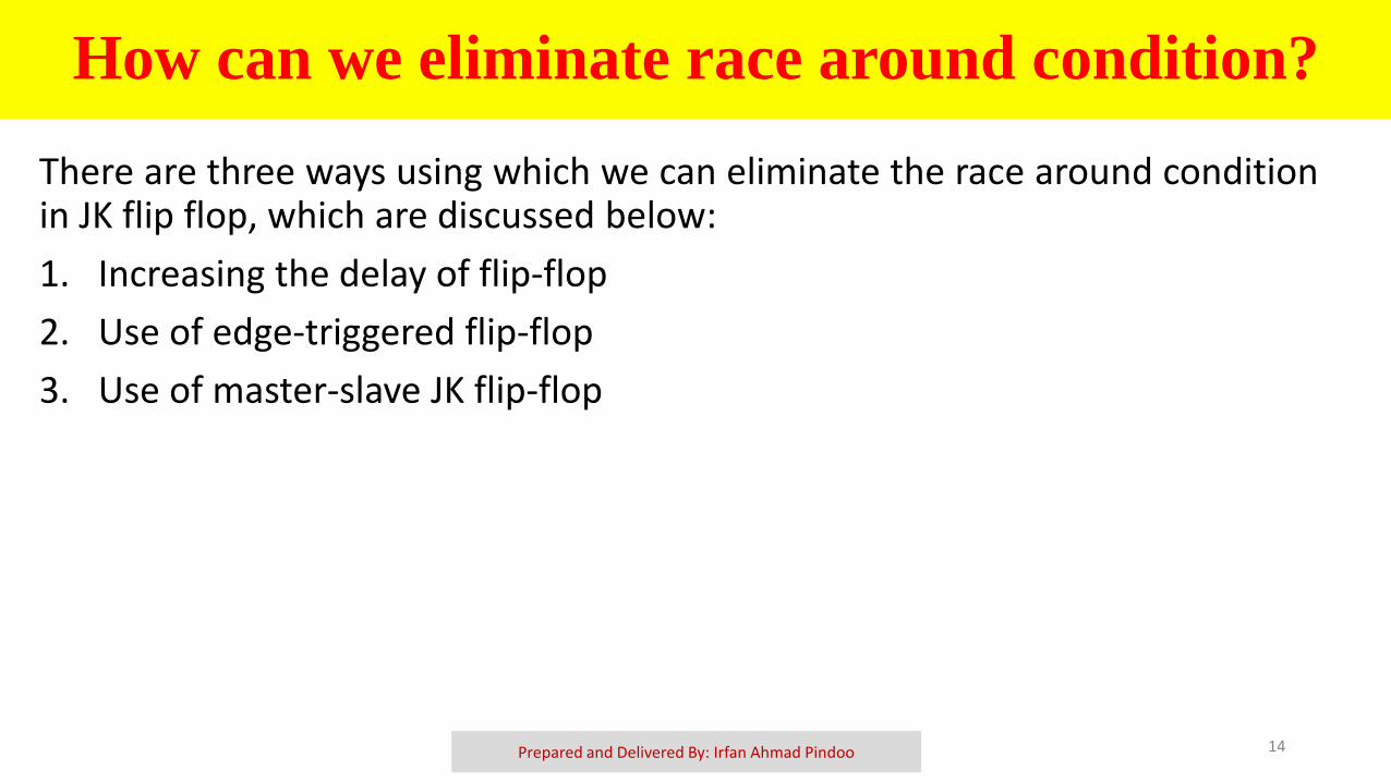
How can we eliminate race around condition?
Prepared and Delivered By: Irfan Ahmad Pindoo 14
There are three ways using which we can eliminate the race around conditionin JK flip flop, which are discussed below:
1. Increasing the delay of flip-flop
2. Use of edge-triggered flip-flop
3. Use of master-slave JK flip-flop

How can we eliminate race around condition?
Prepared and Delivered By: Irfan Ahmad Pindoo 15
Increasing the delay of flip-flop
The propagation delay (delta t) should be made greater than the duration of the clock pulse(T). But it is not a good solution as increasing the delay will decrease the speed of thesystem.
Use of edge-triggered flip-flop
If the clock is High for a time interval less than the propagation delay of the flip flop thenracing around condition can be eliminated. This is done by using the edge-triggered flip floprather than using the level-triggered flip-flop.
Use of master-slave JK flip-flop
If the flip flop is made to toggle over one clock period then racing around condition can beeliminated. This is done by using Master-Slave JK flip-flop.

The condition for race around condition in JK flipflop is:
a) J=1, K=0 and CLK=0
b) J=1, K=0 and CLK=1
c) J=1, K=1 and CLK=0
d) J=1, K=1 and CLK=1
Prepared and Delivered By: Irfan Ahmad Pindoo 16
QUICK QUIZ (POLL)

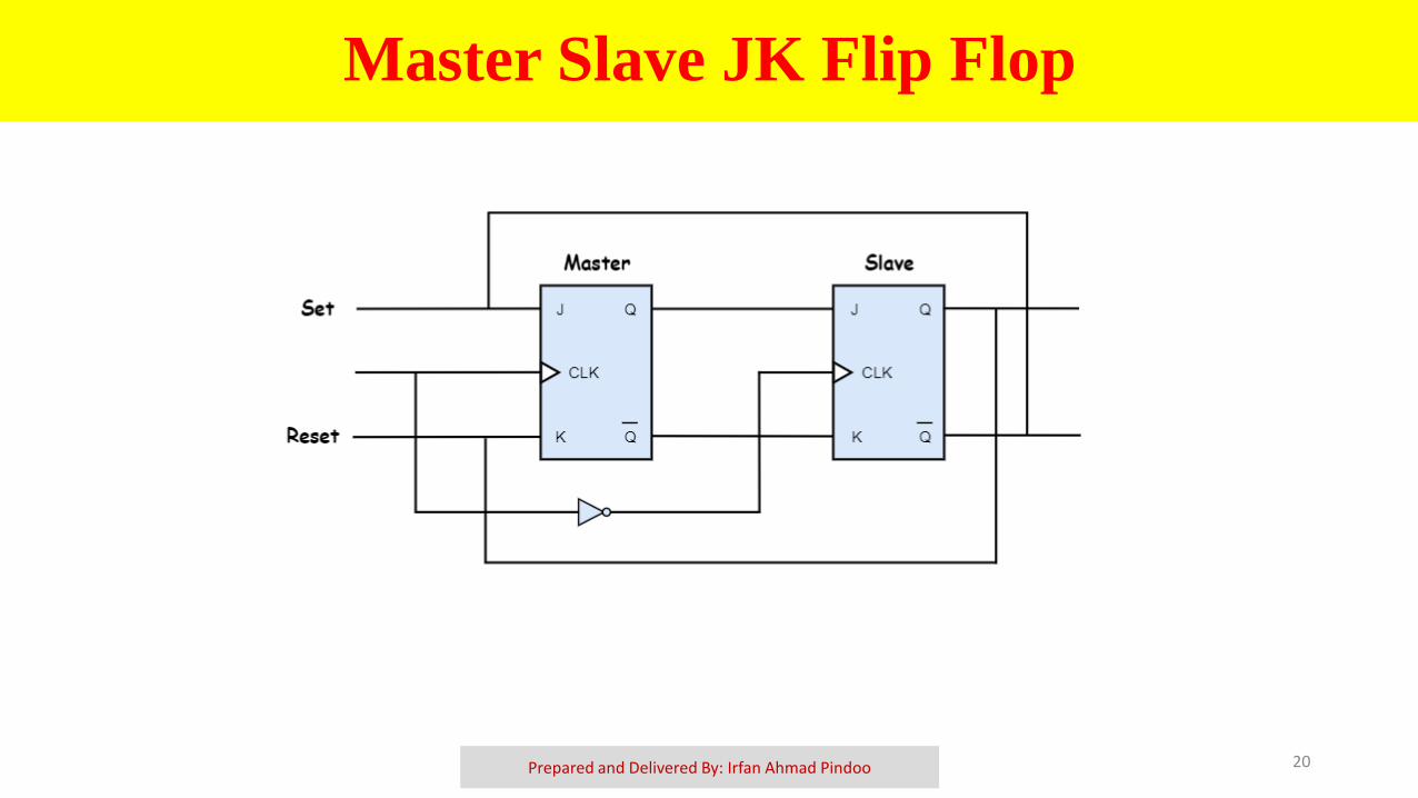
Master Slave JK Flip Flop
Prepared and Delivered By: Irfan Ahmad Pindoo 18
The Master-Slave Flip-Flop is basically a combination of two JK flip-flopsconnected together in a series configuration. Out of these, one acts as the“master” and the other as a “slave”. The output from the master flip flop isconnected to the two inputs of the slave flip flop whose output is fed backto inputs of the master flip flop.
In addition to these two flip-flops, the circuit also includes an inverter. Theinverter is connected to clock pulse in such a way that the inverted clockpulse is given to the slave flip-flop. In other words if CP=0 for a master flip-flop, then CP=1 for a slave flip-flop and if CP=1 for master flip flop then itbecomes 0 for slave flip flop

Master Slave JK Flip Flop
Prepared and Delivered By: Irfan Ahmad Pindoo 19
Master Slave JK Flip Flop
Prepared and Delivered By: Irfan Ahmad Pindoo 20

Master-Slave configuration is designed by using?
a) SR Latch
b) JK flip flop
c) Multiplexer
d) Adder
Prepared and Delivered By: Irfan Ahmad Pindoo 21
QUICK QUIZ (POLL)

Master Slave JK Flip Flop
Prepared and Delivered By: Irfan Ahmad Pindoo 22

Master slave flip flop is also referred to as?
a) Level triggered flip flop
b) Pulse triggered flip flop
c) Edge triggered flip flop
d) Edge-Level triggered flip flop
Prepared and Delivered By: Irfan Ahmad Pindoo 23
QUICK QUIZ (POLL)

Topic: Sequential Circuits, Latches and
Flip flopsUNIT IV:
Lecture No.: 30
1

Suppose we want to know the sequence of the input combination whichresults in a definite output state.
The information pertaining to this can be obtained by back-tracing (in termsof columns) the information presented by the characteristic table of the flip-flop.
Prepared and Delivered By: Irfan Ahmad Pindoo 2
Excitation Table

For the given outputs, the corresponding input states are calculated.
This statement is true for:
a) Truth table
b) Characteristic table
c) State table
d) Excitation table
Prepared and Delivered By: Irfan Ahmad Pindoo 3
QUICK QUIZ (POLL)

Prepared and Delivered By: Irfan Ahmad Pindoo 5
Excitation Table: SR Flip Flop
CLK S R 𝑸𝒏 𝑸𝒏+𝟏 𝑸𝒏+𝟏
0 × × × 𝑸𝒏 𝑸𝒏
1 0 0 0 0 1
1 0 0 1 1 0
1 0 1 0 0 1
1 0 1 1 0 1
1 1 0 0 1 0
1 1 0 1 1 0
1 1 1 0 Indeterminate
1 1 1 1 Indeterminate
Characteristic Table: Excitation Table:
𝑸𝒏 𝑸𝒏+𝟏 S R
0 0 0 ×
0 1 1 0
1 0 0 1
1 1 × 0

If Qn and Qn+1 values of SR flip flop are 1 and 0, the S and R values would be:
a) 1 and X
b) X and 1
c) 0 and 1
d) 1 and 0
Prepared and Delivered By: Irfan Ahmad Pindoo 6
QUICK QUIZ (POLL)

Prepared and Delivered By: Irfan Ahmad Pindoo 8
Excitation Table: JK Flip Flop
Excitation Table:
𝑸𝒏 𝑸𝒏+𝟏 J K
0 0 0 ×
0 1 1 ×
1 0 × 1
1 1 × 0
Characteristic Table:
CLK J K 𝑸𝒏 𝑸𝒏+𝟏 𝑸𝒏+𝟏
0 × × × 𝑸𝒏 𝑸𝒏
1 0 0 0 0 1
1 0 0 1 1 0
1 0 1 0 0 1
1 0 1 1 0 1
1 1 0 0 1 0
1 1 0 1 1 0
1 1 1 0 1 0
1 1 1 1 0 1

How many entries in the excitation table of JK flip flop consist of don’t cares:
a) 1
b) 2
c) 3
d) 4
Prepared and Delivered By: Irfan Ahmad Pindoo 9
QUICK QUIZ (POLL)

Prepared and Delivered By: Irfan Ahmad Pindoo 11
Excitation Table: T Flip Flop
Characteristic Table:
CLK T 𝑸𝒏 𝑸𝒏+𝟏 𝑸𝒏+𝟏
0 × × 𝑸𝒏 𝑸𝒏
1 0 0 0 1
1 0 1 1 0
1 1 0 1 0
1 1 1 0 1
Excitation Table:
𝑸𝒏 𝑸𝒏+𝟏 T
0 0 0
0 1 1
1 0 1
1 1 0

Prepared and Delivered By: Irfan Ahmad Pindoo 13
Excitation Table: D Flip Flop
Characteristic Table:
CLK D 𝑸𝒏 𝑸𝒏+𝟏 𝑸𝒏+𝟏
0 × × 𝑸𝒏 𝑸𝒏
1 0 0 0 1
1 0 1 0 1
1 1 0 1 0
1 1 1 1 0
Excitation Table:
𝑸𝒏 𝑸𝒏+𝟏 D
0 0 0
0 1 1
1 0 0
1 1 1

Which of the following flip flops gives maximum don’t cares in the excitation table?
a) SR flip flop
b) D flip flop
c) T flip flop
d) JK flip flop
Prepared and Delivered By: Irfan Ahmad Pindoo 14
QUICK QUIZ (POLL)

Prepared and Delivered By: Irfan Ahmad Pindoo 15
Conversion of Flip flops
Steps to be followed:

Prepared and Delivered By: Irfan Ahmad Pindoo 22
GATE Problem

Prepared and Delivered By: Irfan Ahmad Pindoo 23
GATE Problem