to my parents - bura.brunel.ac.uk · single boat evaporation in vacuo < 10 -5 torr. all films...
TRANSCRIPT

THE ELECTRICAL PROFý'. ýRTIES CIF PURE MANGANESE ýND
LSE`u'dGAIjF'§ýI, dAQIBISRTV FLUORIDE
CERJM THIN FILM RESISTGRS
A Thesis Submitted by
LOUIS OLU1 KOR
for the Degree of Doctor of Philosophy
BRUNEL UNIVIRSITY
1977
To My Parents
(1)
ACKNOi'lI, ED==
I would like to express my thanks to the following:
Dr. J. Beynon for acting as Supervisor; Professor C. A. Hogarth
for valuable discussions and suggestions; Dr. A. W. Whitaker for
advice on the structural analysis of the films; Mr R. H. Creamer
for discussions on the electrical properties of the films and for
permission to work in the Solid State Physics Laboratory; L: r D. J.
Pacey for permission to use the nigh Vacuum Physics Laboratory;
Dr. B. P0 Betts for allowing the use of certain special equipments;
Mr R. Banerjee for operating the electron microscope; and the
Mid Viest State Govt. for providing a grant for the research pro-
gramme,
I also wish to thank all the work-shop and laboratory techni-
cians who advised and helped with various aspects of the work, viz:
Mr. S. Woodise, Mr L. Lightowler, Mr K. Schlacter, Mr M. Varga,
Mr T. Davies, Mr 11. Krasso, Mr S. Stephens, and Mr Chandrasekera;
Mrs A. Olumekor for encouragement and loss of leisure hours and
lastly to Mrs E. Ackah for typing the thesis.

(ii)
ABSTRACT
Pure Mn and Mr, /MgF2 cermet films (50 to 1500A thick)
containing between 10 and 100 Wt j Mn have been prepared by
single boat evaporation in vacuo < 10 -5 torr. All films
studied are ohmic, and the resistivity lying between 100 w�
SL - cm and 10 m SL - cm. Within this range, the resistivity
decreases non-linearly with increase in film thickness and increase
in Mn content. The effect on the film resistivity of other deposi-
tion parameters, viz substrate temperature, residual gas pressure,
annealing and aging are investigated. The structure of the films
was investigated using X-ray diffraction and transmission electron
microscopy. Films with negative TCR have low activation energies
(r 1 to 100 meV) in the temperature range 110 to 720K, and the
electronic conduction mechanism in these films is probably electron
tunnelling and/or percolation depending on film composition, thick-
ness and annealing temperature.

i ACKNOWLEDGMENTS
ii ABSTRACT
CHAPTER 1'
I INTRODUCTION
1.1 Scope of Thesis 1.1.1 Film Fabrication and Resistivity Measurement
1.102 Results and Discussions
1.1.2.1 Review of Conduction Lechanisms in Thin Films
1.1.2.2 Resistivity Parameters
1.1.2.3 Experimental Results
1.1.2.1 Interpretation of Results%Discussions.
GF: APM 2
2 CO1MENSATION, NUCLEATION lsND GROWTH OF THIN FILMS
2.1 Introduction
2.2 Condensation
2.3 Nucleation
2.3.1 Capillarity Model
2.3.2 Atoaistic Model
2. tß Growth
CHAPTER 3
3 REVIEW OF ELECTRONIC CCIODCTION 12MANISIM IN THIN FZf3dS
3.1 Introduction 3.21 Conduction in Thin Continuous Metallic Films
3.2.1 Thomson Theory

(iv)
3.2.2 Flachs Theory
3.3 Conduction in Discontinuous Metallic Films
3.3.1 Neugebauer and Webb Theory
3.3.2 Hartman Theory
3.3.3 Substrate Effect on Electronic Conduction in
Discontinuous Metallic Films
3.3.3.1 Hill Theory (A) 3.3.3.2 Herman and Rhodin Theory
3.3.3.3 Thermionic Emission
3.3.3.3.1 van Steensel Theory
3.3.3.3.2 Hill Theory (B)
3.4 Conduction in Cermet Films
3.41 Coutts Theory
3.4.2 Christen and Hewitt Theory 3.4-3 Abeles. et al Theory 3.4.4 Gasperick and Navinsek Theory
CHAP=
4 F. XPZR=NrAL APPARATUS
1+"1 Deposition Equipment
1+. 1 .1 The Coating Plant
4.1.1.1 Resistive Heating
4.1 .1 .1 .1 Boat Filaments
4.1.1.1.2 Wire Filaments
1+. 1.1.2 Film Thickness Monitor
1+. 2 Equipment Associated with The Measurement of
Electrical Resistivity
4.2.1 Auxiliar Vacuum Plant
1*. 2.2 d. c. Potentiometer
CFiAFrER_ l
5 EXpERMaTITAL TEM3FIIQüE
5.1 Pre-deposition Preparation

(4)
5.1.1 Cermet Material
5.1.2 Substrates and Substrate Cleaning 5.1.3 Calibration of the Monitor Crystal 5.1.1 Conversion Factors 5.2 Film Deposition and Resistivity Measurement
5.2.1 Temperature Coefficient of Resistance
5.2.2 Initial Investigation
5.2.3 Subsequent Investigation
5.2.3.1 Substrate Temperature
5.2.3.2 Deposition Rate
5.2.3.3 Deposition Pressure 5.2.3.4 Annealing 5.2.4 Structural Analysis
5.2.4.1 X-Ray Diffraction
5.2.1.2 Electron Microscopy
CHAPTER 6
6 RESULTS AND DiSCUSSI0N5
6.1 Introduction
6.2 Variation of Resistivity with Composition 6.3 Variation of Resistivity with Thiclmess 6.4 Variation of Resistivity with Substrate Temperature
6.5 Variation of Resistivity with Deposition Rate
6.6 Variation of Resistivity with Residual Gas Pressure
6.7 Heat-Treatment of Pure Mn and Mr/4X F2 Cermet Films
6.7.1 Annealing
6.7.1.1 Vand's Theory of the Effect of Annealing on
Resistivity
6.7.1.1.1 Estimation of the Lattice Distortion Energy in
Pure Mn Films 6.7.2 lost Annealing Heat-Treatment

(vi)
6.7.2.1 Activation Energy of Unannealed 1 1'91'2 Cermets 6.7.2.2 Activation Energy of Films Annealed at 620,690
and 720K
6.7.2.3 Electronic Conduction Mechanism in Annealed
MIVMgF2 Cermets
6.7.2.1+ Temperature Coefficient of Resistivity
6.8 Reliability of Mn441gF2 Cermets
6.8.1 Performance 6.8.2 Stability
CHAPTER 7
7 CONCLZJSICK
7.1 Proposals for Further Work.

I
CiiAPM ONE
1. INTRODUCTION
This thesis contains the result of a systematic investigation
into the electrical resistive properties of manganese (Mn) and
manganese/magnesium fluoride (g F2) cermet thin films, evapora-
ted onto Corning 7059 Borosilicate glass substrates in vacuo.
Thin metallic films prepared in vacuo have been used for the
68 construction of resistors for over half a century . Initially
their development was slow due to:
(i)
(ii)
poor reproducibility, because the films were fabricated
in rough vacuum conditions. Hence, the resistors often
suffer from a high and varying degree of contamination;
lack of a developed theory to explain the observed high
resistivity of the films;
(iii) little industrial demand for high value resistors. The lower values required(rv kL being adequately provided by
wire wound resistors, composition resistors, carbon
resistors etc.
However, the industrial demand for high value resistors (-+ M)
increased considerably after the advent of radio broadcasting (e. g.
the high input impedance of the triode valve. ) The development of
the electron microscope, of the high and ultra-high vacuum pumps,
coupled with higher industrial demand for miniaturized electronic
components, accelerated the development of thin film resistors after
the second world war.

2
The main requirements for miniaturized resistor components
are:
(i) High resistivity;
(ii) Small size;
(iii) Low temperature coefficient of resistance;
(iv) High thermal, mechanical, and aging stability;
(v) Small 'high frequency' losses;
(vi) Compatible support for the resistor and its connecting leads; and.
(vii) Low cost.
Thin films prepared by vacuum evaporation excel all other types
of resistors in that they can fulfil almost all these requirements.
1arsten 71 has made a detailed survey of the evolutionary steps
leading to the present state of resistors.
The resistivity of a thin metallic film is always higher than
that of its bulk counterpart. The higher resistivity is due mainly
to an increase in the number of structural defects, such as impurity
atoms, vacancies and interstitials, dislocations and grain boundaries.
The use of structural defects to increase the film resistivity is not
feasible in vacuum-evaporated films because the nature of the defects
is unpredictable and the number is difficult to control.
A reduction in film thickness will also increase the resistivity
of a metallic film in a more controlled way. When pure metallic films
are less than b OA, they are usually discontinuous. Discontinuous
films have a higher resistivity than continuous films but they are
also less stable. High resistivity and good stability can be achieved
by introducing an insulator phase into the film to form a cermet
system.

3
1.1. SCOPE CP THESIS
The investigation into the resistive properties of lain and
Mn/bdgF2 cermet thin films may be divided into two sections for
convenience:
(i) Film fabrication and resistivity measurement; and
(ii) Results and discussions.
1.1 .1. Ffl2 FABRICATION AND RESISTIVITY MEASURE1ENT
Film fabrication in this context includes pre-deposition
preparation, such as substrate cleaning and cermet mixing,
instrumentation and instrument calibration, experimental techniques
and a review of the events occunting during film deposition.
The results on instrument calibration are presented under
"Experimental Techniques" (Chapter 5) as they bear no direct relation
to the main result section which deals mainly with Resistivity.
Events occurring during film deposition consist of three
distinct stages:
(i) Transforming the solid evaporant (Mn or M A9F2) into a
vapour phase;
(ii) The movement of the vapour from source to substrate in vacuo; and
(iii) The formation of a thin film by vapour condensation on the
substrate.
Stage (i), solid-vapour phase transformation is purely a
thermodynamic process. Such transformations have not been discussed
as they are well treated in any standard thermodynamic text book.
Similarly, stage (ii) has not been discussed as it is a gas flow

ý
problem which has been covered adequately by a number of
. However, stage (iii) was considered 69
authors ' ýý' *
relevant to this investigation since the resistive properties of
a thin film (for a given thickness, substrate and cermet system)
is controlled mainly by the events occurring at the substrate
during deposition, provided the deposition pressure is sufficiently
low (high to ultra high vacuum range) and the vacuum system is
clean. Hence a review of the process involved (condensation, nuclea-
tion and growth) is given in Chapter 2.
1.1.2 RESULTS AND DISCUSSIONS
Results and discussions in this context mean:
(i) review of electronic conduction mechanisms in thin films;
(ii) definition of commonly measured thin film resistivity
parameters;
experimental results; and
(iv) interpretation of results/discussions.
1.1 . 2.1 REVIEW OF CONDUCTION MECHANISM IN THIN FIUS
The origin of resistivity in thin films is discussed in
, Chapter 3 in the form of a review of the electronic conduction
mechanisms of thin films under the influence of a low do electric
field (5 500 V cm -1 ). The review is also limited to the conduc-
tion processes in plan*r metallic and cermet thin film resistors in
the temperature range 50 to 1000K.
1 . 1.2.2. RESISTIV 7 PARAMETERS
The various parameters used to express thin film resistivity
are defined in Section 5.2.1. An attempt has been made to keep to a

5
unified system of units throughout this thesis. For this reason,
the reader may find that some units in the thesis are different
from those in the original reference manuscripts. For example.,
all weights % and atomic % have been converted into volume %;
temperature and activation energy are expressed in K and eV respec-
tively. '
1 .1 . 2.3 EXPERLN3TAL RESULTS
The experiments were limited to resistivity measurements
obtained with a low electric field (<%5 Vcm )except in one
2.5Vc., i , experiment in which an ac field of less than was applied, in
order to investigate the frequency response of the resistors.
100V do was the highest break-down voltage observed in the test
films. All resistivity measurements were made in the direction of
the applied field along the length of the resistor and in the
absence of a magnetic field. The factors affecting the resistivity
of the films such as percentage composition of the metal, film
thickness, annealing, substrate temperature, deposition rate,
deposition pressure, and the aging stability were investigated.
1.1.2.4- IIVTERPRETATION OF RESULTS/DISCUSSIONS 25,72,73 ' Manganese has certain peculiar properties It
exists in four physical forms having a large variation in bulk
resistivity and structural properties. The results from electron
microscopic investigations enabled comparisons to be made between
film structure and its resistivity.

6
As there were no available data for the MrAgF2 cermets,
experimental results were compared extensively with results of
other cermet systems. For this reason emphasis was laid on the
form (shape of graphs) and the relative order of magnitude of
Mn and M'9k'2 cermets. Whenever possible experimental results
were also fitted to Mown theories.

7
CFIAFrER TWO
2 CONIDENSATION, NUCLEATION AND GROY1T H OF THIN FILMS
201. INTRODUCTION
Due to differences in structure, the electrical properties
of a thin film mayº be quite different from its bulk counterpart.
The structure of a thin film is dictated by a combination of
factors present during the process of film formation. In the
case of films prepared by thermal evaporation in vacuo, the most
important of these factors are:
(i) substrate temperature;
(ii) deposition rate;
(iii) pressure and nature of the residual gases;
(iv) surface mobility of adsorbed atoms on the substrate;
(v) type of substrate (amorphous, monocrystalline or
polycrystalline);
(vi) chemical reaction between substrate and film;
(vii) chemical reaction at the vapour source; and
(viii) presence of an electric or a magnetic field at the substrate.
In the fabrication of I4n4%MgF2 cermet films factors (vi) to (viii)
are not applicable as the substrates used were inert, no chemical
reaction was observed at the source *and
no electric or magnetic field
was applied to the substrate during film deposition. The other
factors are most important at the initial stages of film growth
(Nucleation) which is a problem of vapour-solid phase transformation
(condensation). Although the effect of factors (1) to (v) on the
* information taken from X-ray powder diffraction

8
resistivity of completed Mn and Mn/ gF2 cermets, 100 to 25004
thick was studied (Chapter 6), the condensation and nucleation
processes in these films were not investigated but an understanding
of the processes and theory involved is necessary for the proper interpretation of the structural information. 2.2. CONDENSATION
Thin film condensation from the vapour phase is governed by
the interaction of the impinging atoms on the substrate. An
arriving atom usually has velocity components parallel and perpen-
dicular to the surface. If the substrate is inert, the atom may
either be adsorbed or reflected back into the gas phase. The
adsorbed atom may execute a random motion over the surface of the
substrate, due to thermal activation energy from the substrate
and/or due to its kinetic energy component parallel to the substrate
surface. After a relaxation time, the absorbed atom can re-evaporate
(desorption) or becomes chemisorbed (condensation). Therefore con-
densation is a net result of an equilibrium between the adsorption and
desorption processes. The degree of thermal equilibrium is described
by the accomodation coefficient Ö which is defined as:
Ö= z
T
- E. r
TV - Tr
EQ -E T -T v
(z - 1)
where Ev is the incident kinetic energy of a vapour atom, Er the
energy of an adsorbed atom before equilibrium with the substrate
and E the energy of a desorbed atom after it has equilibrated with
the substrate. Tv Tr and T are the corresponding temperatures. s
The probability that an impinging atom be condensed on the substrate

9
is called the sticking coefficient and it is the ratio of the ý
amount of material condensed to the total amount impinging.
Zany investigators 1,2' 3 have indicated that in the case
of "hot" atoms impinging on a one dimensional lattice W. is less W.
than unity only if the incident kinetic energy is larger than 25
times the energy required for desorption after equilibration with
the substrate. The probability of complete accomodation occurring
=1 increases as the ratio of the mass of an impinging atom to
the mass of a substrate atom increases. In the case of a 3-dimen-
sional lattice, Goodman 4
has estimated that T
becomes unity if
Ev is smaller than the energy necessary for desorption after equi-
libration with the substrate. Thus if the activation energy for
desorption is 0.5eV for example, the incident atom would have to
arrive at the substrate with an energy of 0.775 eV corresponding to
a temperature excess of 6000K before thermal accomodation would
become incomplete. Therefore it appears that except in the case of
either very light atoms or very high kinetic energies, the incident
vapour atoms equilibrate thermally with the substrate very rapidly.
The mean relaxation time required for an incident atom to
equilibrate thermally with the substrate has been estimated by
Lernard-Jones 5
to be less than 2, whereVis the vibrational frequency
of the lattice. According to McCarrol and Ehrlich 6
the adsorbed
atoms will lose all but a few percent of Ev within three lattice
oscillations.

10
2.3. NUCLEATION ý
It is generally agreed that for a thin film to condense into
a permanent deposit, a small number of adsorbed atoms must form
clusters (nuclei) at nucleation sites on the substrate. These
clusters grow by depleting the surrounding regions (capture zones)
of adsorbed atoms so that further nucleation is not possible in the
capture zone. Two models are frequently used to explain nucleation
in thin films, viz (i) the capillarity model and (ii) the atomistic
model.
2.3.1 cAPILAR Tmv MMEL
The capillarity model 7' 8 is based on the classical ca. pill. a-
rity theory for homogeneous nucleation of single droplets of liquid
from the vapour phase, as postulated by Volmer and Webb 9,
and
Becker and Doring 10. The model assumes that clusters are formed
from a supersaturated vapour by the sequential addition of single
atoms from the vapour phase. A condensed phase will be formed if
a stable nucleus is first formed and this will require a positive
free energy. The model also assumes that bulk thermodynamic
quantities are applicable to the properties of clusters. The
-. treatment below essential) follows that of Neu a uer102 The Gibbs free energy 0G Tor forming a spherical truster of
radius r is given by the sum of the surface energy and the volume
energy of condensation , i. e.
G=4,1Tr2d + jjIT r3 Q Gv (2 - 2) 3
where ý GV = -kT In P/pe V
is the Gibbs free energy difference per unit volume. V is the molecular
volume condensed from the supersaturated vapour at a pressure P and e

11
is the equilibrium pressure. P/P is defined as supersaturation
and S is the interfacial energy.
Differentiating equation (2 - 2) with respect to r gives the
radius r of the critical nucleus as:
X= -261& G (2 - 3)
v
X is the minimum size of a cluster required for the formation of
a stable nucleus and the nucleation rate Ir (at a pressure P) under
homogeneous nucleation is given by:
, -v. r !nI\
r= 1411r vr kc-4. j
(2TT mkT) "ý
where V is the condensation coefficient and n* is the equilibrium
concentration of nuclei.
The capillarity model was extended by Hirth and Pound 11 to
include the effect of desorption and of surface diffusion of
adsorbed atoms. They assumed that the surface of a substrate
possesses a density no of adsorption sites for which the free
energy for desorption is Q_des and that surface diffusion is a
"jump" process between adsorption sites, 'characterised by a free
energy of diffusion Q, f" In this case the nucleation rate is
given by:
27Tq'fZr,. aoSia et eir-P (
Qaes Qdifß- Q Ir
- (2TTmjcT) IcT
and z; =dm0 (8) (2 - 6)
- (2 5)
where % (8') is a geometric factor involving the angle of contact

12
A' of the deposit on the surface, Z is a correction factor
allowing for the departure from equilibrium which occurs among
the clusters and m is the maximum free energy and a is the "jump" distance.
In the capillarity model r in equation (2. - 3) is usually
of atomic dimensions. For example if we use the bulk value of
for silver 12
and deposition rate of IAs- at 300K, X is
equal to 2.2 A However the application of the model is
restricted to situations in which the number of atoms in the
critical nucleus is large enough for macroscopic parameters, such
as interfacial energies and angle of contact, to be realistic.
Hirth and Fbund11have suggested that the capillarity model
is valid only for nuclei containing more than about 100 atoms.
Experimental investigations by many workers, among them Walton13a, 13b,
Hirth and Pound 11, and Rhodin and Walton 14 have shown that the critical
nucleus for metals is often less than 10 atoms. This is far below
the critical number of atoms &, 100 mentioned above.
2.3.2 ATO ISTIC MODEL
Walton 13a, 13b and i odin and Walton 14 have suggested that
the difficulties encountered in applying the capillarity model to a
cluster containing a small number of atoms may be overcome by using
the atomistic model. Here they treated small clusters of atoms as
individual molecules and expressed the concentration ni of clusters x
of i. atoms in terms of the concentration no of adsorption sites and
the potential energy gi of decomposition of such clusters into i

13
adsorbed atoms at absolute temperature T, nix is given by :
ý ix ý) l, c (-Eil
expk 0 no
(2 - 7)
where ni is the surface density of adsorbed atoms and the nucleation
rate is given by:
Ir = Drnoa2(Il . n) e
0
r( ix +1) Qaea - Qdiff
kT (2 - 8)
where D is the deposition rate, a the separation between adsorp-
tion sites and '1) the frequency of desorption.
Thus for a very high degree of supersaturation, the critical
cluster may be one atom only (i, 1 = 1) which means that a two-atom
cluster is the smallest stable aggregate. At a lower supersaturatiorl
j. X = 2, a three-atom cluster is now the smallest stable aggregate,
etc.
The atomistic model predicts:
(i) a linear relation between in Ir and 1/T (see equation (2-8) ).
(ii) that the nucleation rate is proportional to the deposition
rate for a constant substrate temperature;
(iii) the nucleation rate is very sensitive to changes in
supersaturation (i. e. substrate temperature); and
(iv) if the size of the critical nucleus changes by even one
atom as the degree of supersaturation alters, a disconti-
nuity will be found in the nucleation rate Vs supersatura- tion curve. Lewis and Campbell 15 have shown that such a discontinuity exists in gold films deposited on rock salt.
The disadvantage of the atomistic model is that it contains para. -
meters which are difficult to estimate.

14
20Z. GROWTH
The nucleation theories in Section 2.3 indicate that there
is a nucleation barrier which adsorbed atoms have to overcome
before they can form a permanent deposit. If there is a
nucleation barrier, then the film will show an island structure
in the initial stages of growth (which is indeed the usual case).
For a very large nucleation barrier, i. e. large critical nucleus
as in the capillarity model (large r ), with a high positive
energy of formation Ei, the film should consist of a small number
of relatively large aggregates after a film of a few monolayers
thick has been deposited. The aggregates are large because their
minimum stable size is large and there are relatively few of them
because the nucleation frequency is relatively small. In the case
of a small nucleation barrier (atomistic model) the film should be
composed of a relatively large number of small aggregates as the
minimum stable size is small and the nucleation frequency is rela-
tively large.
A film consisting of a large number of small islands will
become continuous at a relatively low average thickness. This is
because neighbouring islands grow and touch to form a continuous film
matrix early in the deposition process. On the other hand a film of
only a few big islands will attain continuity at a relatively higher
film thickness on account of the large inter-island separations.
Pashley et al 16 have distinguished four stages of thin film
growth processes, viz:
(i) Nucleation and island-structure;

15
(ii. ) (iii)
(iv)
These
Coalescence of islands;
Channel formation and
The formation of the continuous film.
stages of film growth are shown schematically in Figure 2.1.
Nucleation
i:. .;. """ . "
",.
..
.,, ",,,
. . "". - . ", ". " 4 00&
Hales
I. f .' ý" "e
" f
--30
S
I L.
Continuous Film
Channels
Coalescence 2
"4 04 .
*. 0 J-F-6
Fig. 2.1. The stages of thin film growth (Pashley 16)
When thin film deposition starts, the first evidence of
condensation on the substrate is a sudden appearance of nuclei of
fairly uniform size (Fig. 2.1). The growth of the nuclei is
three-dimensional but the growth parallel to the substrate is
greater than that normal to it because growth occurs largely by
surface diffusion of adsorbed atoms on the substrate, rather than

6 i
by direct impingment from the vapour phase.
Coalescence is assumed to occur only when islands
physically touch each other, the mechanism being analogous
to that of sintering of two spheres 17,18
as shown in
16 Fig. 2.2. Shape changes during Coalescence (Pashley
Figure 2.2. Kingery and Berg 17 have suggested that, during
sintering, transport of material may occur by evaporation
and condensation, volume diffusion and surface diffusion.
Coalescence leads to the formation of larger islands
separated by regions with a much lower density of small
islands than were present at the earlier stage. The smaller
islands are incorporated very quickly into the larger islands
which, as a result become elongated to form a continuous
network structure; the islands are separated by long irregular
and narrow channels (Fig. 2.1).
With further deposition, secondary nucleation occurs in
the channels and the nuclei coalesce with the elongated islands
as soon as they touch .
Eventually, as most of the channels
continue to be filled, the film becomes largely continuous but
contain many small irregular holes (non-filled areas) as shown
in Figure 2.1. Further secondary nucleation occurs within these
holes, as we saw above, until the holes are completely filled.

17
Pashley et al 16 have also observed that some recrystalli-
nation occurs during coalescence even with the substrate held at
room temperature. Recrystallization causes large grain sizes in
the completed film compared with the average separation of the
initial nuclei. In polycrystalline films, recrystallization is
randomly distributed and orientated.
In the condensation, nucleation and growth theories of thin
films given above, it is assumed that a vapour-solid transformation
occurred only during film formation. Semenoff, 19 Palatnik 20
and
Palatnik et al 21 have questioned the validity of this assumption.
They observed the presence of spherical islands in metallic films
of Bi, Sn, Pb, Au, Cu and Al deposited on amorphous substrates at
a temperature Ts> Tm (Tm is the bulk melting point of the evaporant)
P latnik 20,21 postulated that film condensation occurs via
a vapour-liquid-solid transformation. For T. <I Tm, the transfor-
mation occurs directly from vapour to solid. However, in some cases
(such as Sb) the mechanism reverts to vapour-liquid-amorphous solid
for Ts <3 Tm. Support for the vapour-liquid-solid transformation
is provided by the "frozen in" high-temperature metastable phases
of some solids. This is expected on the basis of Ostwald's rule 22
which states that a system undergoing a reaction proceeds from a less
stable state through a series of increasingly more stable interme-
diate states to reach a final equilibrium state. If we assume that
the liquid (or liquid-like) phase is formed as a first step during
condensation (Semenoff 19) and is stabilized by quenching, then
Ostwald's rule suggests that on annealing, we would observe various

18
metastable high-temperature phases of the material. The meta-
stable amorphous phases observed in Buckel's vapour-quenched
films of Bi, Ga and Sb were accounted for in this way.

i 9
GHAE'rER TFPJm
3. REVIEW C*' ELECTRONIC CON JCTION MECHANISMS IN THIN FIU S
3.1. INTRODUCTION
Metals are good conductors of electricity and according
to the modern theories of metals 21., 28 (quantum mechanics),
conduction is due to electron motion through the metal lattice.
From a quantum mechanical view point, an electron will move
through a perfect lattice whose potential is perfectly periodic
without loss of energy, resulting in zero resistivity u
However in practice, the electron loses some energy resulting
in a finite (bulk) resistivity. These losses can occur through:
(i) thermal vibration of lattice ions. This is responsible for a major contribution to bulk resistivity. This
component of resistivity is usually referred to as thermal, ideal, intrinsic, lattice or phonon resistivity;
it is temperature dependent;
(ii) physical and chemical imperfections caused by localised
lattice damage or the presence of foreign atoms. These
contribute a temperature independent component to the
resistivity, and
(iii) size effect and localised spin. These make a negligible
contribution to the bulk resistivity, and are temperature
independent except near liquid helium temperatures.
The total contribution to the bulk resistivity Po of the
various components are contained in Mathiessen's rule, which states
that Po is the sum of two resistivity terms, one due to lattice
scattering J) which is temperature dependent and the other due

20
to imparities, p which is temperature independent i. e.:
Ö- ,c+ /"
(3 - 1)
The variation of /°s with temperature depends on the type of
metal and its relation to the Debye temperature @D' where
eD is given by:
k9. ý hymax (3 - 2)
Amax is the characteristic maximum vibrational frequency of an
atom, h is Plank's constant and k is Boltzmann's constant. At a
given temperature T,, ýO sp(T
for T> GD and Ps OCT 5
for T« 6D.
Bulk metals have resistivities at 295K lying in the range 25
1.5
to 150], )_ SL. -cm.
The resistivity of a vacuum-deposited non-contaminated thin
metallic film is generally considerably higher than that of its
bulk counterpart if the film thickness is of the same order as the
electron mean free path (m. f. p. ). This is because electron
collisions with the film surfaces and the grain boundaries are
no longer negligible. The thickness at which surface scattering
becomes important varies from metal to metal and it is strongly
temperature dependent. Maissel 26
has shown that the electron
m. f. p. for bulk gold is x, 1530 A at 73K, 406 A at 273K and 290 A
at 373K whilst the corresponding value for silver are 2425 , 575 and
405 A at the same temperatures. Metallic films with thicknesses
of the same order as these m. f. p. are usually continuous in
structure.
Deposition parameters also contribute to the resistivity
of thin films condensed from the vapour phase. Matthiessen's

rule for thin films is given by:
ý= Po +Pa +Pb (3 - 3)
where 0a andpb are resistivity components due, respectively,
to size effects and deposition parameters. When the films are
prepared in a clean vacuum system at a low residual pressure
10 _4 torn) and at deposition temperatures above 273K, pa
becomes the dominant part of P.. Thus as the thickness falls, P
increases. However when the thickness becomes extremely small
and the film structure is discontinuous, the increase in p
becomes too large to be explained by thickness effects alone.
A number of theories based on electronic conduction have been
proposed to explain this difference. The development of these
theories and their practical limitations are discussed in the
following sections.
3.2. CONDUCTION IN THIN CONTINUOUS METALLIC FILMS
3.2.1. THOMSON 27 THEORY
Thomson proposed that electronic conduction in thin
continuous metallic films may be due to diffuse internal scattering
of electrons at the upper and lower surfaces of the film. As a
starting point he used the Drude-Lorentz free electron gas model,
which says that the bulk resistivity is inversely proportional to
the electron m. f. p., but made the following assumptions:
(i) all electrons start their motion at the centre of the film, (Fig. 3-1-);
(ii) the scattering of electrons at the film surface is
non-specular, (i. e. the direction of motion after collision is independent of its motion before collision
and
�
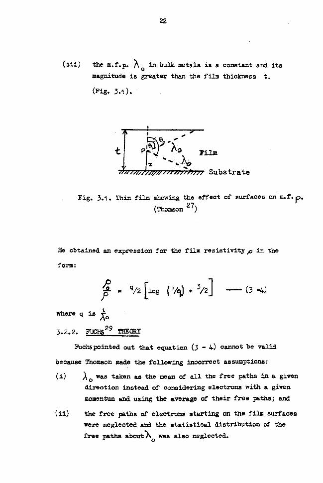
22
(iii) the m. f. p. ?C in bulk metals is a constant and its
magnitude is greater than the film thickness t.
(Fig. 3A).
pr .1 `Qý
_ Film
Substrate
Fig. 3.1 . Thin film showing the effect of surfaces on m. f. P. (Thomson 27 )
He obtained an expression for the film resistivity o in the
form:
iý
P T
where q Is /10
= q/2 Clog 1
ý/ý + 3/2] (3 -+)
3.2.2. F'UCH, S29 THECRY
Fuchspointed out that equation (3-4) cannot be valid
because Thomson made the following incorrect assumptions:
(i) ^o was taken as the mean of all the free paths in a given
direction instead of considering electrons with a given
momentum and using the average of their free paths; and
(ii) the free paths of electrons starting on the film surfaces
were neglected and the statistical distribution of the
free paths aboutX0 was also neglected.

23
(i)
(ii)
Iuchs29 modified the Thomson theory by considering:
electrons whose motion start at the film surfaces and
elastic and inelastic electron scattering at the film
surfaces.
He assumed that in bulk metals the probability that an electron
is scattered with an energy E in time ds is given by ds (E dr
where'r is the mean free time of scattered electrons and is taken
for the highest occupied energy level in the metal. He applied
Maxwell-Boltzmann statistics to those electrons whose motion
begins on the film surfaces and obtained the following expression,
via:
`, o =1 -(3/8q)(1 - p) for q. >> 1 (3 - 5)
P where p represents the fraction of electrons that are scattered
elastically. For complete diffuse scattering p=1 and for
complete specular reflection p=o. Equation (3 - 5) is valid for
thick films only (i. e. films with q»>1 at room temperature).
Sondheimer 30 worked along the same lines as FuchSaid obtained
an expression for the resistivity of very thin continuous films of
the form:
/4(, 1 F) q log /1%q) for q4I1
The main objection to the use of the Fuch-Sonäheimer
resistivity equations is the use of a single parameter p to
describe electron scattering from the upper and lower surfaces of
a film.
24
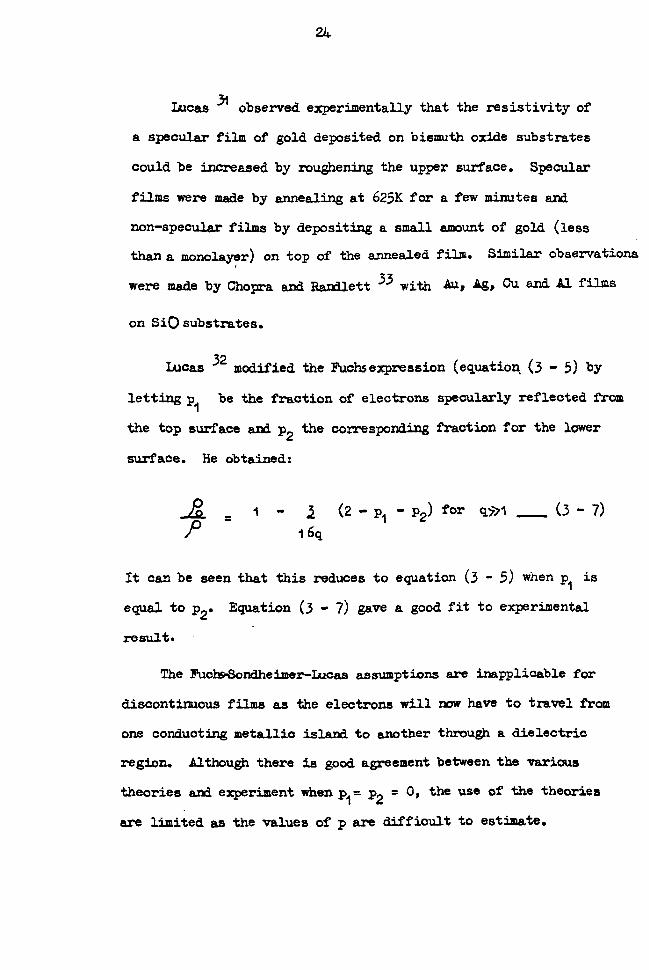
Lucas 31 observed experimentally that the resistivity of
a specular film of gold deposited on bismuth oxide substrates
could be increased by roughening the upper surface. Specular
films were made by annealing at 625K for a few minutes and
non-specular films by depositing a small amount of gold (less
than a monolayer) on top of the annealed film. Similar observations
were made by Chopra and Randlett 33
with Au, Ag, Cu and Al films
on Si0 substrates.
Lucas 32 modified the Fuchs expression (equation (3 - 5) by
letting p1 be the fraction of electrons specularly reflected from
the top surface and p2 the corresponding fraction for the lower
surface. He obtained:
Po _1-1
(2-p1 - p2) for q1 (3 -7)
1 6q
It can be seen that this reduces to equation (3 - 5) when p1 is
equal to p2. Equation (3 - 7) gave a good fit to experimental
result.
The Fuca-Sondheimer-Incas assumptions are inapplicable for
discontinuous films as the electrons will now have to travel from
one conducting metallic island to another through a dielectric
region. Although there is good agreement between the various
theories and experiment when p1= P2 = 0, the use of the theories
are limited as the values of p are difficult to estimate.

25
3.3. CONDUCTION IN DISCONTINUOUS METALLIC FilMS
There are two types of electrically discontinuous films
prepared by vacuum evaporation: films consisting of metallic
islands separated by free space (pure metallic films), and
those having metallic islands separated by an insulating
medium (cermets). We shall consider conduction in discontinuous
metallic films next and return to cermet films in Section 3. L.
The resistivity of various ultra-thin metallic films, a
few Angstroms thick, has been found 34 - 48 to be many decades
(up to 106) higher than the bulk metal resistivity. The tempera-
ture coefficient of resistance (TCR) is negative in contrast to
the positive values for both continuous thin metallic films and
bulk metals. Electron micrographs of discontinuous metallic
films 35' 45,48 show that they possess an island-type structure.
The film resistivity is therefore governed by the transfer of
electrons across the gaps between islands and the negative TCR
suggests a thermally-activated process. The origin of the acti-
vation energy is not clearly understood and many models based on
quantum-mechanical tunnelling, substrate-assisted tunnelling and
thermionic emission have been proposed to explain it.
3.3.1 NEUGEBAUER AND WEBB 38
THEORY
Neugebauer and Webb (N and W) investigated electronic
conduction in ultra-thin metallic films of nickel, platinum and
gold deposited on glass substrates. The films were ohmic at low
applied fields and the film resistivity was found to depend
exponentially on the reciprocal temperature.

26
They postulated that the conduction mechanism in a
discontinuous (island structured) metallic film was due to
electron tunnelling through the vacuum between neighbouring
islands. They assumed that ultra-thin films consisted of identi-
cal spherical islands of radius r separated by a distance d
in a planar array. Tunnelling is possible only between charged
and uncharged micro-particles; an activation energy is needed to
create the charge carriers. In the absence of an applied field
N and W suggested that the only electrons which could be trans-
ferred were those lifted to an energy level of the order of Eb
above the Fermi level of a neighbouring island. Eb is the work
done in removing an electron from an island radius r to infinity.
It is given by:
Zb _=
4TT EoE. r
Here e is the electronic charge, Fi-o the permitivity of free
space and a the low frequency dielectric constant. N and W also
pointed out that electrons are actually removed to a neighbouring
island, distance d away and not to infinity. In this case the
energy B. required is of the form:
ez r1I ýTT%EI r- d+ rl
In the presence of an applied field F, the Schottky effect 24
should be included so that the energy Ed necessary to remove an
electron to a distance d is:
Ed = Ec - deF (3 - 10)

27
The activation energy Ea, under these conditions is obtained
by maximizing equation (3-- 10). Then we have.
_F+ feF (3 - 11 ) 2 (rre0C) 3a=
ýý= ee
At low fields and small r equation (311) becomes:
Ea e2 _-(el
(3 - 12)
Neugebauer and Webb assumed a Boltzmann distribution for
the number of charged islands present at a given temperature
T and a transition coefficient D across all the tunnelling
barriers in order to obtain the resistivity expression:
ýr exp ä (3 - 13) 1' d2e2D
(kT ý
The model predicts that the resistivity of island-structured
films (e. g. platinum and gold 150 A thick) varies exponentially
with inverse temperature and is independent of low electric fields
(up to 500 V cm -1). The model also predicts that the activation
energy decreases with thickness since thicker films consist of
bigger islands (large r)and smaller inter-island spacing (small d).
(See Section 2.14. ).
The main objections to the N and IF theory are:
(i) the model neglects the interaction between charged islands; the number of charged islands can be very high.

28
(ii)
For example at room temperature, 25% of the total
number of islands are charged in platinum films which have an activation energy of 50.6 meV. Thus inter-
actions are extremely likely when the activation energy
is ti kT;
electron micrographs (of N and W) show that the islands
are not of equal size, are not uniformly spaced and they
are not spherical in shape. Therefore the assumption of
a constant transition coefficient D is incorrect, as a large variation in d should lead to a large variation in D.
Neugebauer and Webb only considered electrons tunnelling
from a charged particle to a neutral one but Swanson et al 39 have
considered the contribution to activation energy from both posi-
tively and negatively charge carriers. (i. e. transitions between
neutral and between charged particles as well as between charged-
neutral particles). They assumed that an island receiving an
electron will increase its charge by -e and the donor island will
assume a positive charge. Allowing for image forces 25,51
they
calculated the energy required to charge an island, and obtained
an expression for the activation energy Ea of the form:
Ea =
e2 [i_ rJ () 2r +d
Ni and Th. /Cr films, 50 to 100A thick (from Swanson et x139)
gave activation energies 25 to 50% lower than those of N and W.
The objections raised with the N and W theory apply here also
because the same basic assumptions have been used.

29
3.3.2 HARTNAN M 7IMORY
Neugebauer and Webb did not discuss why a charging of the
micro-particles is necessary nor why electron tunnelling in the
neutral island cannot be the predominant conduction mechanism
since this type of tunnelling would require no activation.
Another possible origin of the activation energy was suggested
by Hartman M, who proposed that it arises from the need for
electrons to be elevated to a higher energy level before
tunnelling can take place when an electric field is applied.
Hartman assumed that the band structure of individual
micro-particle was discrete because of their small size. He
represented the islands by cubic potential wells in which electrons
are only able to move from one excited state to another by quantum
mechanical tunnelling through the gap between adjacent islands.
The energy level in a one dimensional potential well is
given by:
E 2Tr2 n2
2ma2
ý3 - 15)
where n is the principal quantum number (= 1,2,3 ----), m is
the mass of an electron and a is the width of the potential well
(= 2 r). Tunnelling can only occur between the (n + 1)th levels
(the highest occupied level at absolute zero temperature being
the nth level). The activation energy in this case corresponds
to the energy difference between the nth and the (n + 1)th levels.

30
It is given by:
(i)
Ea Irr 2ma2
(2n + 1) (3 - 16)
The main objections to the model are:
it assumes the islands to be a uniform array of cubes. Electron micrographs
38' 45' 1+9 have shown that islands
are neither uniform in size nor in their distribution,
neither are they cubic;
(ii) it is a one-dimensional model and therefore ignores
transitions in the y and z directions. Hence equation
C3 - 16) over-estimates the energy level spacing;
(iii) the model assumes that the ground levels are always
uncrossed by either the applied field or by the statisti-
cal distribution of island sizes. The probability of tunnelling between the nth levels would be high if the
island size distribution caused the ground states to be
crossed when a field is applied.
In all the models discussed in Section 3.3., the role of the
substrate on the conduction process has not been considered. It
us now consider some theories that include the substrate in the
overall mechanism.
3.3.3. SUBSTRATE EFFECT ON ELECTRONIC CONDUCTION IN DISCONTINUOUS
METALICFIIJLS
3.3.3.1 HILL 1+9 THEORY A
Kill proposed that a dielectric substrate has a large number
of trapping sites between its conduction and valence bands; most

31
traps are situated near the band edge and a few in the band
gap as shown in Figure (3.2).
Fig. 3.2.1ergy diagram for transfer
of an electron from island I to II by
means of a trap jump (Hill 49).
When a discontinuous metallic film is deposited on the substrate,
the Fermi level Ef in the substrate becomes aligned with those of
the two neighbouring metallic islands I and II. Band bending
effects were neglected because only the region just below the
metal-substrate interface were considered.

32
If a trap is located at the Fermi level, direct electron- tunreelling between I and II should occur, via the trap and the
process should be non-thermally activated. However, if there is no trap at the Fermi level, elect=ron-tunnelling would occur in two stages:
(i) electrons in I with energy equivalent to Ef could first tunnel into trap A below the Fermi level in the substrate, with the energy difference lost to the substrate lattice. Transition from trap A into II cannot occur as there, are no available energy levels below Ef;
(ii) the electron must be thermally activated into the next available trap B higher than Ef and tunnelling into II
can then occur.
Hill4g testen his theory on gold films prepared on soda-lime
and borosilicate glasses. He measured the current through the
films as a function of the voltage applied across the substrate
normal to the direction of current. The results indicate that the + r4 ns V@r-se
film resistance varies with applied - -=voltage at a constant
temperature. At a substrate temperature of 395K, the resistance
of gold films having an average spacing of 52A decreased from
5.5. kl. at - 75V to about 4.. Ok9,. at 100V for films deposited on 6ut
soda-lime glass, remained constant at 5. O kS2from - 100V to -25V
and thereafter rose steadily to a peak of 12.5kJ1 at 50V before
falling steadily to about 5.0kS2at 100V for films deposited on
Corning glass. The change in resistance was interpreted in terms
of a shift in the position of the Fermi level in the substrate.
Although Hill. 49 observed that the film resistance varied
exponentially with inverse temperature, he did not obtain an
expression for the activation energy.

33
3.3.3.2. HERMAN AND RHODIN 42 THEORY
Herman and Rhodin assumed that charge carriers are located
beneath metallic islands and that electron-tunnelling occurs
between neighbouring islands through the substrate surface. They
postulated that a high density of unfilled electron traps or
surface states exists on the substrate. When an island-structured
metallic film is deposited on the surface, a flow of electrons will
occur across the metal-insulator interface filling some of the traps
until equilibrium is reached (i. e. their Fermi levels come into
correspondence). No such regions are formed in the spaces between
metallic islands and the traps in these spaces will remain empty.
A simplified energy band representation of the surface region
of the insulator as a function of the position parallel to the
surface is shown in Figure 3.3.
1 Conduction band 4. 11 -1
N d ý
Yarle`nce acmx, * "f-rw
_ -Y4 A-3 ý ,b j'
- Uatilled Traps
+ Filled traps
Fig. 3.3. Distribution of traps in
the surface of an insulator between
metallic islands (Herman and Rhodin 42)
: p. 2

3 14.
Let the trap regions under the metallic island be designated
a regions and the unfilled trap regions of the surface
separating two adjacent metallic island, b regions. The energy
bands are considered to be bent by an energy value which is
unknown. It is designated P in Figure 3.3. The energy bands are
also assumed to have a sharp discontinuity where regions a. and b
meet. At absolute zero temperature, the a regions are assumed to
be electrostatically neutral. However, the filled traps in region
a may not be at the same level as the unfilled traps due to image
forces.
For tunnelling to occur between a filled and an unfilled
trap, an activation energy must first be provided by the emission
or absorption of a phonon. This energy is considered to be the
electrostatic energy (N and W model) to move an electron out of a
metallic region into an unfilled trap in region b, midway between
two metallic islands. It is given by:
Ea =
2e2 r1-1 (3-17)
4-TTEoE ̀a a+bJ
The Herman and Rhodin theory combined the Hill 49
and
Neugebauer and Webb 38
models and the final resistivity expression
was very similar to Neugebauer and Webb's equation (3 - 13). The
in objections to the theory are:
{i) the resistivity expression contained two parameters-. 6
, the depth of the surface trap region and n the surface density which are difficult to estimate;

35
(ii) in the derivation of equation (3 - 17) Herman and
Rhodin did not justify why an electron has to be moved
to a distance midway between two metallic islands.
In the substrate-assisted tunnelling models, discussed
above, the effect on the activation energy Ea from large and
small island separations have not been considered. According
to Niffontoff, 50,
at 300K and negligible applied electric fields,
the conduction process is dominated by thermionic emission, if
the island separation is greater than 100A. Let is now look into
this possible mechanism in a little more detail.
3.3.3.3. THMIONIC EMISSION
3.3.3-3.1. VAN STEENSEL 45 THEORY
Van Steensel studied discontinuous films of gold and
platinum, deposited on substrates of barium titanate and quartz,
in the temeperature range 125 to 625K. He found that at low
electric fields, gold has an activation energy of 44 meV in the
low tem, perature region (<250K) and 11+0 meV in the high tempera-
ture region (>250K). He interpreted his results by a thermionic
emission mechanism, an activated conduction process previously
50 36 suggested by Niffontoff and Minn

36
Van Steensel proposed that the activation energy arises due
to the need for the electron to leave a metallic island and enter
into the conduction band of the substrate. He assumed
ý-- Without Voltage
- Voltage V across Insulator
Fig. 3.1k. Energy barrier between two metals(Van Steensel 1+5)
that only electrons with energies equivalent to at least the
maximum barrier height (Fig. 3.1k) are transferred from one
metallic island to a neighbouring island.

37
In the absence of an applied electric field, 'Q(2
is equal
to the activation energy Ea given by:
Ea - fö2= 91 -A Jo (3 - i8)
where d% is. 20, the Simmons correction term due to image Ed
. forces in a capacitor structure. is the high frequency
dielectric constant and d the barrier width.
If the maximum barrier height occurs half way between the
two metallic island, then when a small voltage V is applied,
the barrier height is reduced by approximately eV . From tke 2
24 Richardson - bushman equation we can express the current
flowing from island I to island 2 as:
-fI J1-2= AT 2exp- (Ea - eV) (3 - 19) kT
and that from island 2 to 1 as:
J2 -ý=A
T2 exp - (E +i eY)
kT I (3 ý 20)
where A is the Richardson constant fcr thermionic emission, being
^ý12QA cm 2K -2. Thus the net current density J is:
2AT2 Sink () exp (-Ea%kT) (3 - 21)
which for small values of V, reduces to the ohmic form:
J AT2 XP ( -'Ea/k2)
kT
(3 - 22)

38
In equation (3 - 22) it can be seen that J depends
exponentially on the height of the potential barrier between two
neighbouring islands. This height is decreased when two islands
are close together because of the overlap of the image forces.
It is this proximity effect which is believed to give measurable
currents at temperatures much too low for ordinary thermionic
emission to occur. On this basis Niffontoff calculated that for
nichrome films (work functionr. 5eV) at 300K, J is equal to or
larger than the tunnelling current only if d> 80A, whilst at
200K d must be > 130A.
If thermionic emission is the dominant current mode in
metallic films with large island separation, one would expect this
current to be very small. On the contrary, the currents observed
in films with large island separation at room temperature are many
orders of magnitude larger than that predicted by equation(3 - 22).
For this reason many workers 38' 41' 42 have rejected thermionic
emission as a dominant conduction process in such films. Fill 4
however has presented a comprehensive analysis of electronic
conduction in discontinuous films by taking into account thermionic
emission as well as electron tunnelling.
3.3.3.3.2. HILL 48 THEORY B
Hill proposed that the substrate can either play an active
or a passive role in the conduction process. For the active mode
electrons tunnel through the substrate between metallic islands
whereas for the passive mode, electron tunnelling occurs through
the free space between islands. Hill 48
associated the activation

39
energy for tunnelling with the electrostatic energy of the
the island. He used the same basic assumptions as Neugebauer
and Webb 38 and extended the theory to include the effect of:
(i) varying the applied electric field;
(ii) the barrier height given by the metal-insulator
work, functions; and (iii) active substrates.
His model based on three collinear metallic islands is
shown in Figure 3.5. The injection of an electron into an island
of diameter 2r, is considered to raise the potential of that island
with respect to zero (defined at infinity) by an amount E, given
by:
EI =
e2 i3-23i 47T EC- r
(The symbols have been defined earlier in Section 3.3.1. )
This island will raise the potential of its nearest neighbour,
a distance d away by an amount E2 given by:
E2 =
e2 ý... - (3 -24)
1+7rrE0 E (2r + a)

40
elP
go, x
Fig 3.5. Energy diagram far 3 collinear islands
in an applied electric field. ] is the undistorted barrier height, V is the voltage drop between
islands, and the Fermi level in island b is dE
below that in islands a and c (Hill').
The activation energy is the potential difference between these
two islands. It is given by:
Ea = e2 r+= (3 - 25) 4.71' E. tý r (2r + d) ý-

41
When a small electric field (F. s105 Vcm"') is applied between
the islands, Ea becomes:
Ea =
e2 (r+d Fe (2r + d)
41rE6E r(2r + d) i3 - 26)
For Ea> kT , Hill 48 obtained an expression for the electron
current density J in the form:
Ih eV )TrBkT J_ 28 TTme sin h3 B' kT sin7rBkr
1
exp(+ý)ý exp (ýl
3-27
and for E a
kT , Cautts
51 obtained a corresponding expression:
8Trm8 ey` TrBkT
h3 B kT J Sin7rBkr
where
- exp -- HE8)
exp(gý()' $
i3 - 28)
,
kTr Ad (2m) ' h
ýJ
is the mean barrier height to tunnelling and 4d is the image-
force reduced barrier width. The original expression for J given
by Hill 48 for Ea < kT has been found to be mathematically
incorrect as it predicts infinite current as Ea ) 0.

42
Like Van 3teensel5, ii. ll 48 has indicated that the
conduction process in thin discontinuous metallic films is
determined by the island size and the inter-island separation
Hill concluded that it was possible to classify films into four
types depending on whether the island diameter is large or small
(i. e. whether _
e+2__ > kT and whether the inter-island
4 , Tr CA: r
spacing is greater or less than the tunnelling path length. The
classification is summarised in Table 3.1.
Predominant Activation type of Energy conduction
Small
Small
Table 3.1. Classification of discontinuous
metallic films (Hill 48).

43
Hill 48 also proposed that there are two types of
substrate-assisted tunnelling: Direct tunnelling in which a
bias field has no effect, as in alkali-free substrates; and
substrate-modulated tunnelling in which tunnelling depends on
the presence of free alkali ions. In the latter case he
assumed that, a single ion is situated between each pair of
metallic island with the result that the barrier height is reduced.
The conduction models discussed in Section 3.3. are applica-
ble to discontinuous films of pure metals deposited on insulating
substrates. Conduction in cermet films (metal-dielectric compo-
site mixtures) will now be considered.
3.4. CONDUCTION IN CER! T FILMS
The structure of a cermet film differs from that of an
island-structured pure metallic film in that the inter-island
spacings are no longer separated by empty space but by solid di-
electric material. Consequently the electronic conduction process
will vary with the amount of dielectric in the film. In certain
cermets (Cr/SiO 53,54-and MrVtiO
52,55) chemical reaction
between the components may lead to varying phases (e. g. silicidea)
to be formed at certain metallic compositions. Glang et al 54
have made a detailed study of the structure of Cr/SiO cermet films.
Up to the solubility limit of Si in Cr, the boo Cr lattice is
the stable crystalline phase, and the presence of Cr3 Si is due
to chemical reaction. Hence the films are not homogeneous but
consist of small particles of Cr and silicides in a matrix of
SiO 2.

44.
In the absence of a chemical reaction, Morris 56
found
that the conduction mechanism in Au island structures in SiO and
that of Au/Si in SiO2 could be interpreted by the N and W theory.
On the other hand Coutts 57 suggested that when the metal in the
cermet film is particulate, the N and Ti theory is valid but that
this is no longer the case when the metal is filamentary.
3.4.1. COUTTS 51,57 THEORY
Goutts studied the structural and electrical properties of
gold-Corning 7059 borosilicate glass cermets, prepared by RF
sputtering in argon. The substrates were also Corning 7059. He
observed that the gold either formed capillaries or island
structures. Hence he postulated that these structures gave rise
to two independent conduction processes acting in parallel to one
another.
He assumed that conduction in filamentary capillaries is
analogous to conduction in thin wires having diameters less than
the bulk electron mean free path given by Dingle 58. The resis-
tance R1 due to normal metallic conduction in capillaries at a
temperature T was given as:
lý = RC) (1 + aC 91) (3- 29)
where R. is a constant defined at a temperature To, 91= T- To
and Q( is the TCR.
In the case of the island structure, he assumed an activated
conduction expression based on the N and W theory, viz:
a2 =ý exp (Eal (3 - 30)
kT

45
where R. is given by equation (3 - 25) and R., is a constant.
R0 and R., are constants only for one metal-insulator composition.
If the metal ratio decreases, R0 increases and öo decreases.
The total film resistance R for the parallel system is given by:
8= R1 $2
ý3-31) RI + R2
The capillaries in the films were 40 to 80A in diameter,
but Coutts observed that some capillaries appeared to be broken
up into large elongated islands (ellipsoids), as well as spherical
islands, varying in sizes and separations. On average, the diame-
ters were, 110A and their separations --\j 50A. Using Jeans' 59
electrostatic theory for ellipsoids having two equal short axes,
Coutts modified the activation energy term in equation (3 - 30).
If the gold ellipsoids have axes labelled a, b, and c, where
c represents the capillary length (major axis) then the geometric
mean of a and b (r = (ab) and not c was assumed to dominate the
activation energy (Ea in equation 3- 25). Taking a= 100A and
b= 40A, we find that r r. 63A giving an activation energy of about
40 meV which is within a factor of 2 to 3 of the value of Ea for
the smaller islands (the value of r for smaller islands is not
given but it is assumed to be between 50 and 100A).
As a result of this analysis, Coutts suggested that the ends
of the ellipsoids where the field is greatest were interacting
with the smaller islands. The model will be complicated further

J+6
if the metallic resistances of the larger islands are taken
into account.
3.4.2. CHRISTEN AND HEWITT 60
THEORY
Christen and Hewitt studied the mechanism of electronic
conduction in Au/SiO and Au/Si02 cermet films as the metallic
content of the film was varied. Following Hill's structural
classification (Table 3.1. ), they categorised cermet films into
three structural groups according to their metal-insulator
content:
(i) films composed of isolated dielectric regions in a
continuous metallic matrix, characterised by low
resistivity;
(ii) films composed of isolated metallic regions in a
continuous dielectric matrix, characterised by high
resistivity; and
(iii) a transition region from high metallic content to a
low metallic content characterised by a resistivity
sensitive to both the metal-dielectric volume ratio and
the structural changes during annealing
For group (i) films three dielectric scattering models of
conduction were postulated. These are:
(a) the dielectric particle model ;
(b) the layered particle model ; and
(c) the filament model .
In the dielectric particle model, the dielectric islands are
considered to act as scattering centres for the free electrons in

47
the continuous metal matrix. An expression was obtained in
terms of the ratio of the cermet resistivity to the intrinsic
metal resistivity /P0 ,
viz:
. -JO =
P 1+ Äoa«7T»r2
1-3 . nTrr3
32)
where 1-3n -TT r3 is the volume fraction. Vf
of the metal, r and n are the radius and density of the
dielectric islands, and Xo is the electron m. f. p. in the bulk
metal . The variation of PI) with Vf indicated that film 0
resistivity increases as Vf decreases and also that Pý increases
as r decreases.
In the layered particle model, the films are considered to
consist of alternate ultra-thin layers of metal and dielectric,
there being no metal-metal or dielectric-dielectric layer contact.
In this case the cermet resistivity is given by:
vf p' (3 - 33)
where p is the resistivity of one metallic layer of uniform k
thickness tm; and Vf is given by the ratio:
tm where td is the uniform (tm + td)
thickness of a dielectric layer. They used Fuchs 29 and
Sondheimer 30 theories of electrical conduction in thin continuous
metallic films to obtain an expression for the resistivity of the

48
metallic layer ýO in the form:
L po q
fk) (3-34)
where f(q) is given by equations (3 - 5) and (3 - 6) and q by
tJ " Combining equations (3 - 33) and (3 - 31+), we have:
0
P= r(q) Jýo q of (3 - 35)
A graph of against 1 indicates that /_p is propor- lo of 4
tional to J. for a constant Vf. It was also shown that when tm
m is small compared to td, the film resistivity increases as td
increases.
The filament model assumes that there are numerous small
metallic filaments aligned along the direction of the applied
electric field. Adjacent filaments are separated by a layer of
dielectric. The cermet resistivity is given by:
P= )ro- '-vf, (3 - 36)
where Pf
eis the resistivity of one filament and their volume
fraction Vf-is given by:
vf, _ 6ý (2rf) /i3 - 37)
rf"and d are respectively the filament radius and the distance

49
between the centres of adjacent filaments. If rf. <'ýd, there
is no contact between filaments. For rf'> id, the conduction
process is still assumed to be filamentary but no consideration
was given to the possibility of interaction between the filaments.
The resistivity of filaments has been considered by Dingle 58
and Chambers 61 as:
G, (ý
where q=2 rf
AO
ý3 - 38)
Using Dingle's analogy of conduction in thin wires and Chambers
theory for conduction in thin wires in a magnetic field, Christen
and Hewitt obtained an expression for the cermet-intrinsic metal
resistivity ratio, viz:
ý=1
o vf' ýq (3 - 39)
A graph of against Vflshows that RP
decreases with increase
o ib in rfi ,
The resistivity of films in group (ii) usually lies between
the high values of the dielectric and the low values of the metal.
For this region they suggested that the conduction mechanism is
similar to that occurring in ultra-thin discontinuous metallic films,
where the film is made up of a planar array of islands as discussed
in Section 3.3.
ol

50
Group (iii) films fall into the transition region between
groups (i) and (ii). They suggested that the film resistivity
is very sensitive to change in phase of the dielectric, to small
changes in the metal-dielectric volume ratio and to structural
changes during annealing. In their experiment (P Vs volume
composition of SiO 2 in an Au/Si02 cermet system) it was found
that a resistivity jump occurred at about 50 vol % SiO2. This
resistivity jump is considered to be due to the transition from
group (iii) to group (i. i).
The main objection to Christen and Hewitt theory is that
their models contained parameters which are difficult to determine.
Although they successfully fitted their own Au/SiO experimental
data to theory, as well as Ostrander and Lewis' 76 Cr/SiO
data, when r is 5A, td is 2A and rf, -is 2.86A, the success of the
theory depends largely on the correct determination of these usually
unknown parameters.
3.4"3e ABELES. SHMG. covTrs AND AM 63
THEORY
Abeles et al proposed that conduction in cermet films (they
referred to as granular metal films) is controlled by the amount
of metal and dielectric in the film. Like Christen and Hewitt 60,
they divided granular metal films into three structural groups -
metallic, dielectric and transitional regime.
In the metallic regime, bulk metallic phenomena such as
superconductivity and ferromagnetism 64., 65
which depend, on the
transfer of electrons, are retained but bulk properties such as

51
TCR and resistivity 66
which depend on electron m. f. p. are
greatly modified due to stron, electron scattering from the
dielectric inclusions and the grain boundaries.
As the dielectric material is increased, the metallic
continuum starts to break-up into isolated metallic particles.
At some critical composition which depends on the metal-dielectric
system, the dielectric islands become interconnected and a maze
structure is formed. The resistivity then increases rapidly with
further decrease in the metallic content and the TOR changes sign
(from positive to negative), denoting a transition from the metallic
to the dielectric regime. The authors observed that the transition
regime occurred within the resistivity range I to 10 mQ - cm.
In the transitional regime, conduction is said to be due to
percolation along the metallic maze and electron tunnelling between
isolated metallic islands. The two processes become comparable at
the temperature and composition when the TCR changes sign.
The transition into the dielectric regime occurs at a
percolation threshold metallic composition below which only tunnel-
ling contributes to the conduction process. (Bulk superconductivity
and ferromagnetism are observed to vanish abruptly at the percola-
tion threshold although individual isolated metallic islands can
retain their superconductivity and ferromagnetism if their size
is larger than the critical size required for the existence of
these phenomena).

52
Using a complex capacitor, Figure 3.6, consisting of a
superconductor - insulator - granular metal - metal
(Al - A1203 - Ni Si02 - 9u) they proposed a tunnelling model based
on the assumption that the tunnelling current consisted of two
parts:
oxide Granular Tu. mnelling Metal
I
Ba=ier /
_/ " I
Alt oil,
sibio
(l) (ii)
Fig. 3.6. Metal - Insulator - Granular metal
Tunnel structure (Abeles 63)
electron tunnelling into isolated metallic island from
the insulator, (N and W theory 38) and
electron tunnelling into the metallic cont; nuum -om the
insulator.

53
In this case it was assumed that there is an effective junction
capacitance Ce at the insulator granular metal interface, and the
activation energy E is the charging energy for the capacitor and
it is given by.
E= 2
e
e 20
(3 -40)
The total activation energy in the transition region is the sum of
Ea (as given in equation (3-12) and E (equation (3 - 40) ).
In the dielectric regime, they proposed that the conduction
mechanism is by electron tunnelling and that it was both electric
field and temperature dependent. At low fields kT is taken to be e
much larger than the potential difference V between neighbouring
metallic island+nd an activated tunnelling process predominates
leading to a low film resistivity, given by:
ý_ý exp 2 (C%1tT)'6
where /o is a constant independent of temperature and C is a
constant independent of grain size and constituent metals and
insulators. Equation (3 - 1+1) indicates that is independent of
applied electric fields and that:
T-ý lnýo pL (3 - 1+2)
Experimental results 68
show equation (3 - 42) to be valid for
granular metal films of Pt/SiO 21 Ni/Si02 and Au/A1203 in the dielec-
tric regime.

54
At high fields, thermal-activated and field-enhanced
tunnelling are the main conduction mechanism, with the latter
becoming dominant when the resistors are non-ohmic. The transition
from low to high field occurs when V becomes comparable or greater
than 1. They assumed that the potential difference across neigh- e
bouring metallic islands is a constant value, so that the entire
structure is divided into parallel equipotential surfaces perpendi-
cular to the direction of the applied field as shown in Figure 3.7.
IE
Fig. 3.7. Illustration of equipotential
surfacesin a granular metal when an electric
field E is applied (Abeles 63).
The high field F, low temperature resistivity Pi given by: E
where E 0
= eam (ý (3 -43) Poo F
C
ew and w is the separation between equipotential layers.

55
Equation (3 - 1+3) indicates that /PH is independent of temperature
and that
pp In /H ý( F (3 - 1a )
These authors obtained a good fit of experimental data to
theory (equations 3- 41 and 3- 43) for both low and high electric
fields applied parallel and perpendicular to the plane of film.
3.4. -4. GASP"r. xIC AND NAVIlVSEK 67 TMXRY
Gasperic and Navinsek proposed a conduction model for cermet
thin films (planar resistors) containing 5- 30 vol % metal follow-
ing a systematic investigation of electronic conduction in Cr/SiO
system. They assumed that a cermet film is analogous to a three
dimensional array of cubic bricks of equal sizes, with each layer
consisting of metal and dielectric cubes arranged alternately.
Such an arrangement constituted a combination of resistorSin series
and the resistivity p is given by :
v fý= jm' m+ Il vi i3 - 45)
where and V are respectively, the resistivity and volume fraction
with the subscripts m and i referring to metal and insulator
respectively. As «' equation (3 - 45) reduces to:
PxP, °j. (3 - 46)

56
To enable JJ to be calculated,, they used Stratton's 85
equation
for the current density in an insulating film between two metallic
islands to obtain pi,
viz:
22.8 exp
{i.
025 ti (ý 100. ), %-
in 0.5125TTkT (3 -47)
where ti is the thickness of the insulating layer ý the mean
barrier height and m* is the ratio mi with mi being the mass of
mm
an electron in the insulator and mm the electron mass in the
metal.
Gasperic and Navinsek stated that if Pi is known, it is
possible to predict the resistivity of a cermet film (using this
model) to within one or two orders of magnitude for films containing
up to 60 vol % of the dielectric (5 to 30 vol jc metal only). Hence
the model is applicable only in the dielectric regime.
These authors were able to fit experimental data to theory
for the Cr/SiO cermet system. They used a equal to 0.5, Pi
values from computed fÖ values in the range 0.1 to 1 eV and ti
values of 0 to 50A (using a metallic island thickness of 15A
obtained from electron micrographs). Hence the success of the
theory depends on the accurate determination of these parameters
which usually suffer large deviations from their mean values.

57
CHAPTER FOUR
b-. EXPERIKENTAL APPARATUS
into:
cl)
The experimental apparatus may be conveniently divided
deposition equipment; and (ii) equipment associated with the measurement of
electrical resistivity.
1+"1. DEpOSITION EQUII3'W
The deposition equipment consists basically of:
(i) a coating plant;
(ii) a film thickness monitor; and
(iii) a set of deposition masks.
1+. 1.1. THE COATING PLANT
The films were prepared by thermal evaporation in a 305 mm
vacuum coating plant (Edward model 12E3), illustrated schemati-
cally in Figure 1+. 1. The work chamber (Figure 4.. 2) is cylindri-
cal, 305 mm diameter and 362 mm high. It is sealed at the bottom
with a stainless steel top-plate 305 mm diameter and 13 mm thick.
The base plate carried all the electrical feed-throughs, the
shutter operating lever and a tripod stand, which supports a
stainless-steel metal plate 240 mm in diameter and upon which is
mounted a quartz crystal monitor (monitor cystal), a substrate
heater and thermocouple wires. This plate also served as the

58
Fig 4.. 1. Schmatic diagram of a vacuum coating plant,
support for the specimen holder. All the electrical leads within
the chamber were insulated electrically and thermally with alumina
beads (see Fig. 1.. 2)

59
Fig. 4.2. The coating plant showing the work chamber
The chamber was evacuated with a diffusion - rotary pump
assembly. The diffusion pump was an oil type (throat.: "-meter
101.5 mm) capable of attaining an ultimate pressure of 5x10 -7

60
torr if silicone pump fluid (Dow-Corning MS 704) is used.
A single stage mechanical oil sealed rotary pump (having a dis-
placement of 11.4 m3 hr - 1) was used for evacuating the main
chamber from atmosphere and for backing the diffusion pumpe The
pumping system was able to reduce the chamber pressure to 1x10 -'
torr in 5 minutes and to 5x10 -6 torr in 90 minutes, as monitored
with a Penning cold-cathode ionization gauge. The backing
pressure and the pressure in the main chamber during the rough
vacuum stage were monitored with a Pirani gauge.
A liquid nitrogen trap (Dewar type) was used to reduce back-
streaming and back-migration 74, thus reducing the risk of oil
contamination. There is also a tube of Al 2 03 balls to reduce
back-migration from rotary to diffusion pump. All elastomer seals
in the system were of Viton because they have low out-gassing
properties at temperature up to n, 1+75K"
The coating plant is also provided with solid-state, fully
variable high and low tension power supplies (3.5 kV/50 mA, 30V/
30A and 10V/90A). The low tension power supply was adequate for
all evaporations carried out in the system. These evaporations
were performed using resistive heating.
4-. 1 .1 .1. RSISTIVE-EEATL'`TG Fn. A1"4F. AFl'-S
Two forms of filaments were used; boat-shaped tantalum foils
and tungsten wire spirals.

61
1-. 1.1.1.1 BQAT FILAMENTS
The boats used were approximately 15 mm long, 5 mm wide
and 5 mm high with support flanges of about 10 mm long at each
end. (Fig. 4.3). The evaporation area of the boat approximated
a finite strip surface source 75.
ý 15mm ý. 1 0mm _ýý
I_ 5ma
fi Fig. 4.3. Boat-shaped filament made of Tantalum.
The single boat offered a convenient way of evaporating an
element (Mn) and a compound (MgF2) with relatively close melting
points (1525 and 1538K, respectively at a pressure of I standard
atmosphere) Tantalum was found to be a suitable boat material
as pure Mn and bin%29F2 mixtures do not readily wet or react with
it at the evaporation temperatures.
A great advantage of the single boat is that deposition can
be carried out at constant rates whilst the percentage composition
of the cermet is varied. Its main disadvantage is that the ratio
of Mn to Mg72 is by weight. Hence the proportion of Mn in the starting

62
composition is assumed to be the same as that of the deposited
film as X-ray fluorescence was not available. This disadvantage
was greatly reduced by putting a regulated amount of* t'roroughly-
mixed Mn/(gp2 cermet powder in the boat and carefully operating
the heater filament controls to avoid spitting.
A double-boat system (Edward model E19A3 coating plant)
consisting of two independently operated single boats was used to
prepare some films for selected investigations; Mn was put in one
boat and 11gF2 in the other (Fig. 4.4. ). The disadvantages of the
ML W2 8waporati o. n Sources
Fig. 4.4. Two boat arrangement yielding a
variable film composition and thickness.

63
double boat system are that percentage compositions are expressed
in volume % which are obtained by adjusting the evaporation rate
of Mn with respect to Mg? 2 or vice-versa. As we shall see later
in Section 6.5, changes in the deposition rate causes changes in
film structure and resistivity. Also to obtain films of uniform
composition and thickness, the positions of the boats, the monitor
crystals and the substrate become critical (Fig. 4.4. ). A
detailed account of thickness distribution as a function of
substrate position has been given for the Cr/SiO cermet system by
Ostrander and Lewis 76.
4.1-1-1.2. WIRE FILAMENTS
Multi-stranded tungsten filaments in spiral form were prefera-
ble to single stranded loop filaments for the evaporation of manganin
and aluminium. It was found that the loop filament has a life span
of only 3 to 1 evaporations before it developed acute necking as a
result of evaporation of parts of the filament. In contrast, the
multi-stranded filament provided up to 12 evaporations.
4.1-1.2 FILM THIS MONITOR
The film thickness monitor (Edward model 1) was used for
monitoring the thickness of the film during deposition. The equip-
ment employs two AT cut crystals operating in a fundamental thickness
shear mode 77.
A monitor crystal (oscillating at 6MHz) has a depo-
sition area of 21.59 mm3 and was housed in a crystal can which was
placed 267 mm above the boat and 35 mm from the centre of the
substrate. A reference crystal (oscillating at 6.5 MHz) was housed

64
in a steel box outside the deposition chamber.
The two frequencies are mixed and the difference amplified.
After implication, the resulting frequency is again mixed with the
frequency from a variable local oscillator (in the amplifier circuit)
to give a final difference of 0 to 150 kiss. During film deposition,
the resonant frequency of the monitor crystal is reduced to give an
increase (or a shift) in the final frequency difference. The fre-
quency shift and its rate differential are displayed on meters.
Before use, the thickness monitor was calibrated for Mn and tO2
cermets, as detailed in Section 5.1.3.
1+. 1.1.3 MASKS
Two out-of-contact mechanical masks were used for resistor
fabrication, one for the resistor tracks and the other for the
electrical contact pads (Fig. )+. 5)
ThBU
Fig. 4.5. Desposition Masks.

65
The masks were made from a thin sheet of molybdenum, /copper alloy
(15 mm x 15 mm x 0.5 mm thick), and the resistor tracks (15 mm
x3 mm) and the contact pads (5 mm x5 mm) were produced by photo-
lithographic techniques. The original pattern for the contact pads
was later modified (Fig. 4.5) to allow for the two longer pads
required in four terminal electrical measurement of resistance.
The masks were spot-welded onto a mild-steel frame 3 mm thick,
102 mm x 51 mm external dimensions and 78 mm x 27 mm internal dimen-
sions. The frame also served as the substrate holder during film
deposition.
IF. 2. EQUIPMENT ASSOCIATED WITH THE MEASUREMENT 0'
ELECTRICAL RESISTIVITY
Two distinct sets of apparatus were used for the electrical
resistivity measurements:
(i)
(ii)
an auxiliary vacuum plant, for measurement in vacuo
e+ 5x 10 _4 to 5x 10 -6 torn; and
a direct current potentiometer for measurements carried
out in air.
4.2.1 AUXILIARY VACUUM PLANT
The auxiliary vacuum plant was a conventional type consisting
of a work chamber; a liquid nitrogen trap and a diffusion-rotary
pump assembly. (It was designed and assembled from locally
available parts in the department. )

66
The work . chamber was basically cylindrical (Fig. 4.6) but
with four smaller cylindrical projections arranged vertically and
horizontally in the direction of two cross diameters. It was made
of stainless steel 300 mm in diameter and 300 mm long. There are
two access points into the chamber: a front swing door (360 mm in
diameter and 12: mm thick) which is fitted with a glass window
(153 mm in diameter); and a brass top top plate (200 mm in diameter
and 12 mm thick).
Fig. 4.6. The work chamber of the auxiliary vacuum plant.

67
The chamber walls and the door are water-cooled, thus reducing
outgassing at elevated temperatures. The horizontal cylindrical
projections from two side areas which carry all the electrical feed
throughs into the chamber. All leads inside the chamber were insu-
lated electrically and thermally with alumina beads.
The liquid nitrogen trap was of the Dewar type and the level
of liquid nitrogen in it was automatically maintained by a Croyflow
submersible Dewar pump (type CSMPB) in conjunction with an automatic
level sensor (ALN LI+) for liquid nitrogen (Edward High Vacuum Products)
Thus maintaining a fairly constant rate of back-streaming and back-
migration (oil contermination) at all times and at all temperatures.
The specimen holder and its heating and cooling assemblies
were all incorporated in a single unit (Fig. 4.7).. The cooling
section is basically a liquid nitrogen condenser (95 mm x 70 mm x
82 mm) which is attached to the top plate by a steel pipe (Liquid
N2 refill pipe). Copper was used for the top and bottom of the
condenser, but the walls were made of stainless steel to reduce loss
of heat by conduction.
The hot stage consisted of a copper block (60 mm x 45 mm x
10 mm) welded onto the base of the condenser with maximum thermal
contact. Nine equally spaced holde5 (3.5 mm diameter) were drilled
through the copper block, and into which thermally recrystalised
alumina pipes (3.5 external diameter, 1.3 mm internal diameter and
60 mm long) were inserted. A nichrome wire(1.2 mm diameter) looped

68
through the pipes formed the insulated heater element.
The substrate recess (27 mm wide and 2 mm deep) runs along
the middle of the copper block. This recess was planed and
polished so that the substrate had intimate contact with it.
Further the substrate was held in position by four spring-loaded
contacts on an asbestos block which in turn was clamped firmly
onto the condenser by a pair of brackets (Fig. 4.7). The ends of
the spring-loaded contacts were highly polished as they also
provided the electrical contacts between the thin film and the
connecting leads. With this arrangement it was possible to cycle
the temperature between 110 and 720K without admitting air into the
system.
Temperatures above room temperature were obtained by passing
a d. c. current through the heater element and the current was
provided by a 30V/10A (Farnell model B 30/10) continuously variable
power supply. The film temperature was monitored by two Comark
electronic thermometers: type 1623 Cu/Con for low temperatures;
and type 1602 Cr/Al for high temperatures.
The d. c current flowing through the test sample was provided
by a stabilised power supply (Coutant model LA 100.2) which was
fully variable in the range 0 to 30V and 0 to 2A) and capable of
operating in either a constant current or a constant voltage mode.
The current flowing through the test sample was monitored with an
auto-ranging digital multimeter (Keithleys model 168) which has an
accuracy of 0.1% on the current range. Another digital multimeter
(Advance Instruments model IN M3) with an accuracy of 0.1% on the

69
voltage scale monitored the potential difference across the
Fig. 4.7. The specimen holder showing its heating
and cooling assemblies.
test sample. The diagram for this arrangement is shown in
Figure J.. 8.

70
$eifi, hleys 168
iý
22ii. n lila Register
Contact pad ý
Advance Instrument DXK 3
Fig. 1+. 8. Four Terminal resistance measurement.
4.2.2. D. C. POTENTIOMETER
A direct current potentiometer (Croydon Precision Instruments
type 2) was used to measure the p. d. across the test sample when
a current of ImA flows through it. The measuring circuit (Fig. 4.9)
consists of a dial having 17 steps of 0.1 volts and a calibrated
slidewire (152.1+ mm diameter) covering -5 mV to 105 mV with the
smallest division being 0.5 mV. The instrument has 3 ranges:
X 1; X 0.1; and X 0.01 with accuracies of 0.02,0.03 and 0.04
respectively.
Yaraell s 30/i o

71
.. " I.. " 4
0 ý--
Cýý T-T-T
6 1""
u}' u... u+. ý ?., ý, u
ý. ý, _ ý r--- -----ýý -- 2A
1f --ý\ 17
O- b-
ýý
ö, 6 1. -ý ý.. ý; , ýý,..
_t ý.
Fig. 4.9. Circuit diagram of d. c. potentiometer
The potentiometer has an independent standardising circuit,
which is not affected by the operation of the main dial. The
circuit incorporates a compensator which automatically corrects
for the variation in the voltage of the standard cell, due to
changes in environmental temperatures. The null position of the
potentiometer was determined with a moving coil galvanometer
(VrPA type K107) having a sensitivity of 54.0 mm/ A.

72
5.
(i) pre-deposition preparation; and
(ii) film deposition and resistivity measurement,
5.1" PRE.! -DEPOSITION PREPARATION
A description is given in this section of the various steps
taken prior to film fabrication. It also includes films deposited
for use in the calibration of the monitor crystal. However such
films were not used in investigations involving resistivity mea-
surements.
5.1-1. THE CERMET MATERIAL
The component materials used for the cermet mixtures were
manganese of 99.9% purity, (Griffin and George Ltd. ) and magnesium
fluoride, 4- 40 mesh, (British Drug Houses Ltd. ). Prior to mixing ,
the magnesium fluoride was ground into a fine powder using a pestle
and most r- Then several grammes of the required mixture (10 to
100 Wt % Mn) were weighed in an Oerton balance, (with an accuracy
of ± 0.1 mg). Further grinding ensured that complete homogeneous
mixing was obtained. Only a small amount of the mixture (e, few
milligrammes) was used at a time. This was ground again immediately
before use to ensure that the mixture remained homogeneous.
CHAFM FIVE
EX NTAL TECHNIQUES
This chapter contains two main sections:

73
5.102. SUBSTRATE AND SUBSTRATE CLEANING
Thin films were condensed on four types of substrates:
Corning 7059, alkali free alumino-borosilicate glass for electrical
resistivity measurements, and cellulose acetate paper, Kapton and
freshly cleaved mica for structural investigations.
The glass substrates were washed in running tap water to remove
dust adhering to them due to electrostatic charges. They were than
loaded, five at a time, onto a silica glass rack and immersed in a
degreasing solution containing one part of Decors detergent to 100
parts of de-ionised water held at bout 375K for ten minutes. The
rack was then transferred to another beaker containing de-ionised
water to remove the detergent from the substrate; to accelerate this
process boiling water was used. Then the substrates were cooled in
de-ionised water at room temperature for a few minutes before the
rack was moved into a drying chamber containing isopropyl vapour.
This type of drying was preferred because it does not require
a freshly distilled isopropyl alcohol for every cleaning run.
Occasionally water marks were left on the substrates in areas where
they were in contact with the rack. This problem was eliminated by
placing the rack on a clean tissue for about 20 seconds between the
final rinse and the drying. This cleaning method was unsuitable
for the other substrates (mica, cellulose acetate paper and Kapton)
which were degreased by immersion in freshly distilled Isopropyl
alcohol at room temperature.
7'+
5.1.3 CALIBRATION OF THE MONITOR CRYSTAL
The general description and mode of operation of the
monitor crystal is given in Section 41.1.2. However, before the
crystal can give a standardised measurement of film thickness, it
must first be calibrated using an absolute optical method, viz. by
relating the frequency shift obtained during film deposition to the
measured thickness of a material of known density (e. g. aluminium).
A number of frequency shifts, reasonably spaced, were selected
and aluminium films of corresponding thickness were fabricated using
the resistor masks described in Section 4.1.1.3. After the resistors
were fabricated, a reflective coating of aluminium was deposited to
cover them and the entire surface (film side only) of the substrate
so that a step was produced at each resistor boundary.
The height of this step (film thickness) was measured using a
multiple-beam interferometer 75. A linear dependence of frequency
shift on aluminium film thickness was obtained as shown in Figure 5.1.
Using Figure 5.1 the frequency shift of various compositions of
Mn and Mn4 gF2was obtained by relating their densities to that of
aluminium and using suitable conversion factors.
5.1 . 4.. CONVERSION FACTORS
If an aluminium film density d1 and thickness tj, is produced
by a frequency shift of f1 then 78

74a
500
.. Y / O
iA W
ý
ID
ti1 F4 Pti
1 Alm
ý
ý
500
200 -
100L
4 12 20
Fitt T icknress / 10 2ä
1
Fig. 5.1 Fregmeac7 Shift Ws Alum - iita Fitt Thick ess

75
For a cermet having the corresponding parameters d2 and t2, the
frequency shift is given by:
f2 0"'c12 t2 ( 5- 2)
Combining equations (5 - 1) and (5 - 2) we find that:
f2 =ä,
t1 t2 (5 - 3)
11-
where f1 is the slope of the graph in Figure 5.1. If the t1
conversion factor d2 is known, f2 can be calculated for any d1
chosen value of t2 (or vice-versa) within the sensitivity range
the thickness monitor. d1 is known (for aluminium d1 = 2.7g cm
at 273K) and d2 was obtained as follows:
d2 = m2
= mass of cermet
V2 Vol. of cexmet
but
V2 = v3 + V4 (5 - 5)
--- (5 - 1+)
where V3 and V. are respectively, the volumes of Mn (density d3)
and Mg72 (density dd) in the cermet.
If x is the weight percentage composition of Mn then from
equation (5 - 5)
of
-3

76 .
x (1 2
R2 pý.. p MZ + 100
m i5 - 6) d3 d4
Substituting for V2 in equation (5 - !. ) and dividing by dý we find that:
d2 =
d1 rýý "ýi
100 d3 T 100
I
00 -x .1 4
The calculated conversion factors for the various Mr1gF2
compositions are shown in table 5.1. The relationship between
the expected film thickness for Mn and Mr6gF2 based on the above
mathematical calculation and the observed thickness from optical
measurements was also investigated for a number of selected films.
The expected film thickness were ± 15% of the measured value.
5.2. FILM DEPOSITION AMID RESISTIVITY MEASUREMENT. '
Before commencing to describe the technique used for film
deposition and resistivity measurement, here are some relevant
definitions and derivations of some of the commonly measured
resistance parameters and their importance.
A thin film resistor prepared by vacuum deposition is usually
rectangular in shape. For a given mask, the resistor length 1 and
width w are constant so that the film resistance R is directly
proportional to the resistivity and inversely proportional to the
thickness t.

77
wt. %
100 90 80 70 60 50 40 30 20 10 0
Density of carnet
g. oae 3
7.400 6.541 5.861 5.309 4.853 4.468 4.140 3.857 3.610 3.393 3.200
Deasi Conversion of Al factor
9 'es 3 d2/d1
2.700 2.741 2.423 2.171 1.9" 1.797 1.658 1.533 1.428 1.337 1.257 1.185
Ceraat tt l. thick-
seng t2 ý_
5.00
Yregnency shift x5Z 10-2kas
Table 5.1. Frequency shifts calculated for Mn/MgF2
cermet films 500A thick using conversion factor d2ýd1
R i6 given by:
52.24 46.62 41.14 37.47 34.25 31.60 29.22 27.22 25.48 23.95 22.58
I
R

78
As 1/w is a constant (Aspect ratio), equation (5 - 8) can be
mormaZised, i. e.
R= Rs-9 1 (5 - 9)
where R. (= P/t) is the sheet resistance and it is usually
expressed in units of ohms per unit square (c. /Q ).
Rs is a useful parameter for comparing thin films particu-
larly those of the same materials deposited under similar conditions,
as a knowledge of the film thickness is not required. A more
accurate film comparison can be made using resistivity,
If t is known, the film resistivity pp (= Cr- , where d is
the conductivity) may be obtained from equation (5 - 8) to give:
/0 = 8t (i7) (5 - 1o)
p has units of ohm - cm (SZ - cm) and it is the most widely used
parameter for describing a thin film resistor, because it enables
us to compare films of different materials and thickness.
5.2.1. TEMPERATURE CCEF'FICIENT OF RESLSTANCE (OR RESISTIVITY)
The Temperature coefficient of resistance
defined at a given temperature T as:
ýt = 81 R2
RT -7 -T2)
(5 -11)
(TCR) G: R is
for TI >T> T2, where PT is the resistance at a temperature T,.

79
and R, and R2 are resistances at temperatures T, and T2
respectively.
When the TCR is small, as in some thin films QGR is obtained
from the R Vs T curve. Here TCR is defined as:
iy, R =R' Cdý - 12)
Similarly the temperature coefficient of resistivity is defined
as:
a, ý_/O
%dp1 dT j (5 -13)
For thermally activated conduction j
(ý, ý - /" kT
since _ exp
(at dw
+t+W
i5 -ý 4)
It is usually assumed that (X is equal to O(. . This is valid
only if the linear coefficient of thermal expansion Q(, T is negligible.
By differentiating equation (5 - 10) and dividing the result by ýp
or its equivalent we have:
dp 14
"1 d1© _ ýý fý dT
1 dR
( 3a/kT)
1 dl x dT 17 4TT-
(5 - 15)
since» dý +
dw

80
i. e.
aý Q 0(-r (5 - 16)
For bulk metals XT < 10 -2 Q(ý so that 9 is equal
to Q(R is valid. Due to expansion missmatch between the film
and its substrate this is not the case for thin films. Ila, l 79
has shown that aT can be as high as 65 ppm K -1 for fused glass.
These values are significantly large as they are comparable to
TCR values for cermet and thin metallic films. However (, YT can
be reduced considerably with the right choice of substrate as
shown in Table 5.2. Corning 7059 lies in the fused silica group.
Substrate Material
Fused Silica Soda-Free Glass Beryllia Soda Lime Glass
C1T (96) at 775K
0.03 0.22 0.32 0.45
Table 5,2. Percentage linear expansion of various substrate materials
80 at 775K

Si
Hence aP can be equated with for pure Mn films and Mn, /MgF 2
cermet films.
Electrically discontinuous metallic and cermet films
exhibit a non-linear negative TCR whilst thick films and bulk
metals have a positive TCR. On this basis TCR gives an indication
of the structure of a thin film (and hence its resistivity).
From Matthiessen's rule, the bulk resistivity Ao is given
by equation (3 - 1), viz:
/0,0 - ps + ýi
where is temperature dependent and /0i temperature independent,
If we differentiate with respect to T we have: 0
d Do =d
ps (5 -17) dT dT
combining equations (5 - 13) and (5 - 17) we find
Ao OCO , aPg D(8 (5
- 18)
that:
It follows that for a thin film (as expressed in equation (3 - 3)
,pa= Po oao (5-19) If the deposition parameters, and size effects are assumed to be
constant Equation (5 - 19) predicts that the TCR for a thin film
must be lower than that of the bulk metal sincep >> P 0
82
5.2.2.3WITIAL INVESTIGATION
Initially, pure Mn films and MOgF2 cermet films were
deposited onto clean Corning 7059 glass substrates in vacuo
at a residual gas pressure of 1x 10 -5 torr (not rising above
2x 10 - 5torr) from a tantalum boat-shaped filament (see
Section J+"1.1 .1. ). The films were deposited at low rates'L 4.
1As -i.
The substrates temperature was maintained at 295 + 4K. The
cermet composition was varied between 100 and 10 wt %i Mn in
10 wt % steps. For each composition, a range of film thicknesses
was used: 100,250,500,750,1000 and 1500A. The resistor
tracks were fabricated first followed by a subsequent deposition
stage in which manganin conducting pads were prepared at room
temperature. The thickness of the contact pads was not monitored,
but they appeared to be very thick from visual observations and
their sheet resistance was less than 0.0152110 . The contribution
of the contact pads to the film resistivity was negligible, as
the lowest sheet resistance measured was 29.6. QJ Q,
Each film has to pass a visual test before any electrical
measurements were made, The visual test consisted of holding the
film against room light in order to detect the presence of pin-holes
or nonuniform colouration in the specimen.
After fabrication, connecting leads were soldered onto the
manganin contact pads. The four terminal resistance measuring
technique was used for all the resistivity measurements. Although

83
a preliminary experiment to compare the two and four terminal
methods gave an identical result, the four terminal method was
chosen because it provided a more rigid mechanical connection at
the soldered joint.
The test resistor (Fig. 5.2 was connected across terminal 1
min ý 2". ý, n ý Z. ºýwý
_ý
ý
12 mm
I I. I I_ 5mm
MM
Contact Pad
Resistor Traci
Fig. 5.2 Test Resistor
of the potentiometer (Fig. 4.. 9). After standardising the poten-
tiometer, a current of 1mA was passed through the specimen and the
potentiometer was balanced to give a null deflection. Then the
direction of the current was reversed and the reading was repeated
in order to obtain a mean value of resistance.
The current flowing through the sample was increased in stages
during certain investigations to determine the break-down voltage
of the resistor. After the resistance measurements were made, the
test samples were Stored in a dessicator under a rough vacuum, and

84
the film resistivity was calculated from the measured resistance
using equation (5 - 10). The readings were repeated twice on
every occasion a freshly prepared film was used: In cases where
there were large variations in the resistivity value, further
readings were taken until the reasons for the large spread were
ascertained.
5.2.3 SUBSEQUENT INVESTIGATIONS
In the initial investigation, the films were fabricated at
fixed deposition parameters. This section describes the procedure
by which some of those parameters were varied and how the resulting
film resistivity was measured and the film structure analysed.
5.2.3.1 SUBSTRATE TFKFERATtTRE
The investigations carried out in Section 5.2.2 were repeated
with the substrate held at different temperatures'(325,375,395,
425 and 455K). Films were not deposited at substrate temperatures
lower than 290K, as the system was not provided with a cooling-
stage for the substrate. The back of the substrate was heated by
thermal contact with a mica insulated heating element. Prior to
film deposition the temperature of the substrate was gradually
raised to the required values and held there for 15 minutes in
order to attain thermal equilibrium. The temperature was monitored
on the film side of the substrate and at equilibrium it was not
allowed to vary by more than = 48.
The highest deposition temperature (455K) was determined
partly by the outgassing level of the chamber, as the pressure was
not allowed to rise above 5x 10 5 torr, and by the safest maximum

85
controllable temperature. After film fabrication the substrate
was allowed to cool down for at least 1i hours. This being the
the average time taken for the substrate temperature to fall from
4+55 to 295K after the heaters were switched off. In this investi-
-i gation the deposition rate was maintained at 4. As
5.2-3.2. DEPOSITION RATE
The variation of film resistivity with deposition rate, other
parameters being kept constant, was investigated for three film
compositions (100,80 and 60 wt % Mn). Before this investigation was
was carried out, the deposition rate meter calibrated as follows:
films of given thicknesses and compositions were prepared. The
reading of the rate meter (arbitMsry'units in divisions per second)
was recorded for each thickness and the deposition time (s) noted.
The rate meter reading was converted into a deposition rate (As )
by dividing the film thickness by the deposition time, i. e.:
deposition rate = rate meter reading = Film thickness (As -1) (div s -1) deposition time
The required deposition rate was selected by regulating the
boat filament current -- . with the coarse and fine current
controls of the low tension power supply and the selected deposition
rate was kept steady (using only the fine current control) for about
20 seconds before the film were prepared. During film condensation
the deposition rate was not allowed to rise above + 0.1 As for
rates less than 5As 0.5 As for rates less than 10As and
+ 2As -i for rates less than 15As -1 and + 4As -' for those less
than 25As -1. These limits were averages obtained in trial runs
at the specified deposition rates.

86
5.2.3.3. DEPOSITION PRESSURE
The effect on film resistivity of the residual gas pressure
(other parameters being kept constant) was also investigated.
The investigation consisted of two parts: in the first part, the
pressure in the chamber was reduced to 5x 10 -6 torr, then dry
air was bled into the chamber until the required air-pressure was
obtained whilst in the second part the chamber was again evacuated
to 5x 10 -6 torr, then it was flushed with 99.9 % pure argon
(British Oxygen Company) for about 10 minutes at a residual gas
pressure of 5x 10 _4 torr. In either case the required argon or
air-pressure (5x10 -6ta 5x10 -+ torr) for each deposition run was
carefully controlled by adjusting the needle value to the chamber
and the pressure was held at that level for about 30 minutes prior
to film deposition.
5.2.3.4 ANNEALING
The films (deposited by the method described in Section 5.2.2. )
were transferred into the measurement chamber (Section 2+. 2.1).
Aluminium was used for the contact pads instead of manganin because
it was found that excessive mass diffusion occurred at the resistor/
manganin contact pad boundaries (Fig. 5.3)when the substrate
temperature was raised to a high value (> 575K). This effect was
not observed with resistors having aluminium contact pads.
The substrate temperature was raised at a rate not exceeding
4K min -1
until the required annealing temperature (375 to 720K)
was reached. The temperature was then held at this level throughout
the annealing time (1 to 3 hours). The resistance of the film was

87
`4) I1111 (s)
uni Fig. 3.3 100% Un films with manganin contact
pads (a) before annealing (b) after annealing
at 620K for 1 hour.
continuously monitored throughout this study.
When the annealing process was completed, the substrate
temperature was lowered (at the rate of 4. K min '-') to 110K and then
raised again to the annealing temperature at the same rate. This
cycle was repeated several times to determine whether the resisti-
vity exhibited an hysteresis. The resistance was again monitored
continually during the temperature cycling. In some investigations
the temperature was allowed to stabilised for about 15 minutes
at pre-set temperatures before any readings were taken but these

88
readings were similar to those obtained during the cycling periods.
An investigation was also carried out to determine the varia-
tion of resistivity with temperature for unannealed films. The
procedure was basically the same as that given above for the
annealed films except for the substrate temperature which was cycled
between 110 and' 295K.
5.2.4 STRUCTURAL ANALYSIS
5.2.4.1 X-RAY DIFFRACT ION
The composition of the starting materials: Mn, MgF2 and
-- ''g F2 mixtures were investigated using the Debye-Scherrer X-ray
diffraction technique 86.
M Cu radiation (35 KV, 30 nA) was used
throughout the investigation. Both the specimen preparation and
camera loading were carried out in the conventional way 86,87.
The lattice spacings were measured and the structure identified
using the ASTl X-ray powder data file.
Attempts were made to determine the structure of the thin
films (Mn and Mn%MgF2 cermets) using two different X-ray methods:
(i) the X-ray transmission technique. Here the diffraction
pattern is produced by a beam of x-rays passing through both
film and substrate; and
(ii) the X-ray glancing angle technique 88. Now the incident beam is reflected at the film surface. The glancing angle was 0 to 15 0.
In either case the test films were 500,1000 and 2000. in thickness
and were deposited on Corning 7059 glass, Kapton and Mica. Also
the test specimen was rocked.

89
The transmission technique was unsuccessful because the
X-rays were considerably absorbed by the substrates. In the case
of the glancing angle technique,, the specimen caused considerable
scattering of the incident beam with varying efficiency because the
X-rays were not monochromated. The diffraction patterns obtained
were too weak and the information was insufficient to identify
accurately any film structure.
5.2.4-2 =CTR0N MICROSCOPY
The structure of the deposited films were analysed using a
transmission electron microscope (JEM 7). The films used for
structural analysis were deposited simultaneously with those for
the electrical measurements (Sections 5.2.2., to 5.2.3). Initially
the films were deposited on cellulose acetate paper. These were
removed by dissolving the substrate in a solution of methyl acetate.
However, it was found that cellulose acetate paper was unsuitable
for high temperature work as structural and chemical damage occurred
above 395K. Several attempts were made to detach Mn and Mn g? 2
cermet films from Corning 7059 glass pre-coated with carbon by
soaking in dilute hydrofluoric acid 57,
but these attempts were
unsuccessful because the acid attacked the films.
In investigations where it was found necessary to anneal the
films at temperature greater than 395K, freshly cleaved mica pre-
coated with carbon (> 500A thick) were used. The test film was
detached by floating the substrate in de-ionised water. In either
case the film was collected on a copper grid and, after drying
inserted into the microscope.

90
Various areas of the film were viewed and representative
micrographs and diffraction patterns taken. The island and inter-
island separations were measured from the electron micrographs
whilst data for film structure were obtained from the diffraction
patterns, The diameter of the rings enabled the lattice spacing
to be calculated using Bragg's law. These calculations require a
knowledge of the electron microscope camera length.
To obtain the camera length, a gold film, 25QA thick was
deposited on cellulose acetate paper. Representative diffraction
patterns of the film were taken as described above. The diameter
of the rings were measured and the ring number with their corres-
ponding intensities noted. Using the lattice spacings for gold
given in the AST6i X-ray powder data file, it is thus easy to estimate
the camera length. The camera length L is given by 90:
L
x (5 - 20)
where r is the radius of a diffraction ring, d the lattice
spacing and A is the wavelength of the radiation (= 0.042L at 80kV
and 0.037A at 100kV)
Structural and electrical resistivity investigations were also
carried out on the aging properties of films stored in vacuo and on
the open shelf at atmospheric temperature and pressure. The experi-
mental procedure was the same as that described above for films
deposited on glass and mica simultaneously. In addition the resis-
tance of the film deposited on glass was measured at set intervals
of time and their structural investigation was made on a cut out
portion of the film deposited on mica.

91
CHAPTER SIR
6. RESULTS AMD DISCUSSIONS
6.1. INTRODUCTION
For the sake of clarity, the results of experiments
described in Chapter 5 are presented in sections; each sections
relates to one type of experiment and also includes a discussion
of the results. In the discussions, reference is frequently made
to experimental results for other cermet systems. Some of the
data are expressed in Volume % (Vol Atomic % (At %) and
Weight % (Wt %) but mostly in Vol. %. To make the comparison of
Wt, % Mn. I
ýol: ý
100 90 80 70 60 5* 40 30 20 10
"
100 79.55 63.36 50.22 39"34 30.18 22.38 15.63 9.75 4.58
Table 6.1. Conversion table for Mr; /Mg'2
cermets from Wt % to Vol %.

92
these data with those of Mn/MgF2 easier, an attempt was made to
convert Vol % and At % into Wt %, but the information given by
most of the authors was insufficient to make this possible (e. g.
the resistor width and length are not usually quoted). Therefore
Wt % and At % were converted into Vol °/o. The equivalent Vol
M4/MgF2 cermets are given in Table 6.1.
The experimental results of the effect of MgF2 insulator
phase on the resistivity of Mn under different deposition parameters
and film thicknesses will now be presented.
6.2 VARIATION OF RESISTIVITY WITH COMPOSITION
The variation of resistivity with composition for the Mn%MgF2
cermet system is shown in Figure 6.1. The graphs show that the
film resistivity rises gently, and almost linearly in the case of
films deposited at 375K, as the Mn content falls, until it reaches
a certain critical composition. Beyond this composition, the resis-
tivity rises fairly steeply, as the Mn concentration falls further*
As can be seen the change in slope is not abrupt but occurs
gradually over a range of compositions, the extent of which appears
to vary with film thickness. For example for a film thickness of
250A this range is small, viz from 30 to 40 Vol % Mn, but becomes
broader as the film thickness increases to 1500A, in which case the
critical composition region is not apparent even at 22.5 Vol % Mn,
the final composition studied.
This broadening of the critical composition in the thicker
films may indicate that oontizious paths of Mn are formed as the

10-4j_ 95
S
75 55 vaiwrs'6 Mn
35
22-a
Fig. 6.1 Rsaiativity ra Casp+os, ition of ldn/YgI'2

93
film thiclmess increases, thus maintaining the resistivity at
a low level.
Figures 6.2a, 6.2b and 6.2c are transmission electron micro-
graphs for 100,63 and 39 Vol % Mn films, 250A thick. These show
that the size of the metallic islands in the cexmet films decreases
and their separation increases as the proportion of Mn decreases.
MR/Y83'2
cerset coupp- sition( ol
Island
radius ) (A)
Island
separation (A)
Activation Energy
(Key) _
100 81-3--j 21.1 333, _1 85 24.6 ± 6.0
63 37.3 ± 9.0 428 + 139 59.9-. ± 16.4
39 21.4 ± 4.0 714 ± 190 108.0 ±_21.5
Table 6.2. Variation of island radius,, island
separation and activation energy with composition for films 250A thick.

ia) 1 00% Mn
(b) 63Yo1% Mn
(c) 39Ya1% Mn
0 .5 5}. M
L 0.55RMi
0.55 m
Fig. b. 2 Electron Liicrographs/Diffraction patterns of Mn and Mn/Lig12 films 250A thick.
93a

94
The activation energy for conduction was calculated from
the electron micrographs using the Neugebauer and Webb theory 38
(see Section 3.3.1). The results are shown in Table 6.2. It can
be seen that the activation energy increases as the Mn content in
the film is reduced, which is in agreement with results obtained
from resistivity measurement (see Section 6.7.2.1).
Structural investigation detected three distinct phases of Mn:
gamma 2UMn at 1001", Mn, - Mn at 63 Vol % Mn and 0e-. Mn at 39
Vol % Mn. These results (Table 6.3) confirm that no chemical
reactions occurred between the starting materials and the tantalum
Ya/YgIý2 ceraet compo Icýeatiticatioa sition(ýol )
100 Manganese (I)oziae, gamsa 2. U Mn.
63 Manganese (II ) ozicie, A Ma, a Mg? 2.
39 ltmo2 (pyrolnsite ). ý( ý, Or MgF2 ýrMný
Table 6.3. Composition of Mn and Mr; /MgF'2 oermet
films 250A thick.
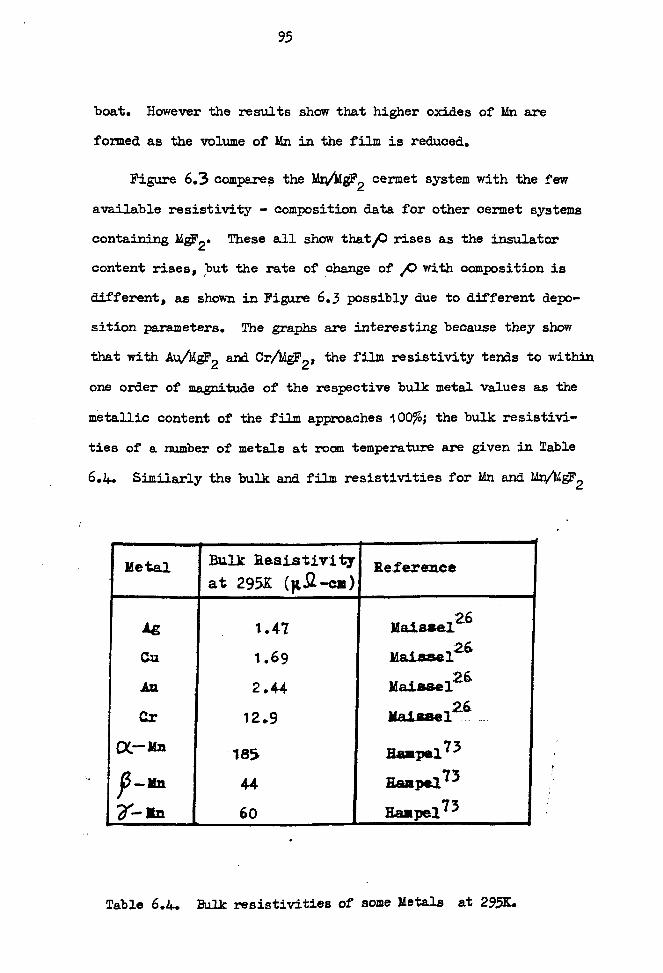
95
boat. However the results show that higher oxides of Mn are
formed as the volume of Mn in the film is reduced.
Figure 6.3 compares the Mm/MgF2 cermet system with the few
available resistivity - composition data for other cermet systems
containing MgF2. These all show that/O rises as the insulator
content rises, but the rate of change of ,O with composition is
different, as shown in Figure 6.3 possibly due to different depo-
sition parameters. The graphs are interesting because they show
that with Au/MgF2 and Cr/4gF2, the film resistivity tends to within
one order of magnitude of the respective bulk metal values as the
metallic content of the film approaches 100ö; the bulk resistivi-
ties of a number of metals at room temperature are given in Table
6.4. Similarly the bulk and film resistivities for Mn and Mr; /MgF2
Metal Bulk Resistivity
at 295K ()t. Q -cm)
Reference
Ag 1.47 Maissel`26
Cu 1.69 Maisse126
fn 2.44 Maissel2-6
Cr 12.9 1dalsse l2-6 __
a Un 185 gas<pa173
mn l 44 ELamp&173 ý= Rn 60 g; aape273
Table 6.4.. Bulk resistivities of some Metals at 295K.

fý
10-4
10-5
r-
r
P-
k-
-
I I
(ft Ya/W2 deposited at 3? 5K (Olmekor )
© Aw' W2 deposited at 31iä (BecýCe n aced _hm
81)
Cr/ß�r2 deposited at 31Eä (Back emn and 81 )
95 75 55 Yvi, axa¢ letal
35
95a
Fig-6-3 BesSstitity Ys Caupa®ition of Yetal/MgF.

96
films agree within one order of magnitude, of the value for
0(-Mn if the latter is always used for bulk manganese. It can
be seen that the bulk resistivity of gamma 2U Mn is about three
times lower than that for cC -Mn (Table 6.4) . As o(- Mn was identi-
fied in the 63 and 39 Vol % Mn films (Table 6.3), it is also possi-
ble that O(- Mn'is partly responsible for the observed increase in
10 with increase in MgP2 content.
Figure 6.3 also helps to support the Fuchs- Sondheimer theories
(equations 3-5 and 3- 6) which state that the resistivity of a
thin metallic film is dependent on its bulk metal resistivity. This
figure shows that for 100%o metal.. Mn thin films have the highest
resistivity followed by Cr and Au thus agreeing with the data in
Table 6.4..
Comparing Cr/SiO with Au/SiO in Figure 6.4, we see that the
former has the higher resistivity. However when these systems are
compared with M3VMgF2 we find that at high metallic content 45 to
85 Vol % metal) the film resistivities of all but Cr/SiO 81 are
within the same order of magnitude but differ markedly as the
metallic content is decreased. Unlike AujMgF2 and Cr/Mg? 2,
the
Au/SiO and the Cr/SiO graphs appear to be generally parallel to one
another, although the Cr/SiO system 83
shows a "double-critical"
composition region. Also it may be noted that the Mn/SiO system 55
shows a resistivity peak at about 85 Vol % Mn. Both the double
critical composition region 83
and the resistivity peak 55
have
been attributed to the formation of Cr and Mn silicides respectively.
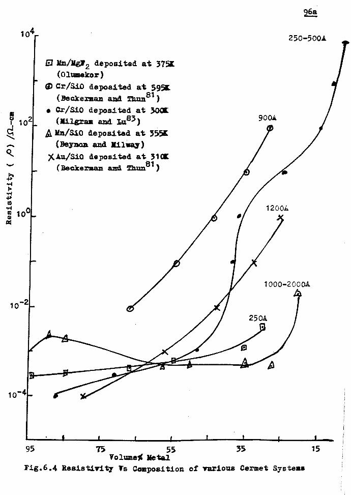
CQ6a zz
1o4,
..
10-4 ý
( Mn/W2 deposited at 37511 (Olumekor )
m Cr/Si0 deposited at 595L (Beckerman and Thun81)
" Cr/SiC deposited at 300[ (Milgra and Lu83)
Q Mn/SiO deposited at 3558 (Beynoa and Mi1wa )
)(Au/SiO deposited at 31 Cz (Beckerman and Thunß1)
250-500A
95 75 55 35 15 volume% Metal
Fig. 6.4 Resistivity Ts Composition of various Cermet Systess

97
The convergence of film resistivity towards the same order
of magnitude has been observed by Neugebauer 66
for the Cr/SiO,
Cr/Si02, NiCr/Si02, Cr/Si, Au/SiO and Aq/SiO2 cermet systems.
He postulated that regardless of metal or deposition conditions,
one curve alone gives a good fit for all metal/SiO cermet films,
because their resistivities are determined only by the extent of
volume dilution of the metal by the SiO or SiO2. This conclusion
seems doubtful because certain deposition parameters have been
found to cause drastic changes in Mn/MgF2 films 82,91,92 (see
Sections 6.3 to 6.7). Figure 6.4 also shows that the postulate is
only correct within a range of compositions (1±5 to 85 Vol j metal).
Beckerman and Thun's results (Figure 6.3) also show that Neugebauer's
postulate is not valid for Cr/MgF2 and Au/MgF2 cermet films with
more than 65 Vol % of metal.
It can be thus seen that the resistivity of all carmet films con-
taining MgF2 increases only by about two orders of magnitude between
85 and 15 Vol%metal whilst the resistivity of'those containing SiO
increased by over four orders of magnitude. Also at 25Vol% metal, cermet
films containing Aft are at least about two orders of magnitude lower
than those containing Au and Cr. A combination of these two components
(Mn and MgF2) gave a resistivity increase of about one order of
magnitude from 85 to 25 Vol% Ma.
6.3. VARIATION OF RESISTIVITY WITH THICK =S
The variation of resistivity p with Mn and Mn/IW2 cermet
film thickness is shown in Figure 6.5. It appears to consist of
three distinct regions labelled A, B and 0 for convenience.

B I
-M ý
i r ! l i i
i i
c
400 800 2200 Thickness /A.
Fig. 6.5 Reais tins ty Ts ? hickness for 1st/XgF2 Cerme is
Deposition Teaperaturs 3751 Depoai tian Pressure l. z? p-5. Deposition Rate 41x-1
7

98
Region A (< 100A) is characterised by a sharp rise in /0 for a small fall in film thickness. For example 0 is
700Lt32- cm for a 100A thick film of composition 63 Vol % Mn Land
rises to about 0.25 Q- cm at 50A.
No electron micrographs were taken for films of 50A thickness
but those for the 250A (Fig. 6.2) show a discontinuous film
structure consisting of discrete metallic islands separated by
dielectric. Hence region A must be characterised by such structural
discontinuity. However, the dielectric spacing in this region will
be larger and the metallic islands smaller. In the cermet films,
such dielectric spacings are composed of MgF2 and free space if the
metal/insulator composition is to be preserved.
All films investigated showed an amorphous structure. The
resistivity in this region is mainly due to the small size of the
metallic islands and their large intermetallic islands separations.
Films in this region were found to be highly sensitive to various
deposition parameters, such as substrate temperature (Section 6.4),
deposition rate92 (Section 6.5) and deposition pressure 82 (Section
6.6), especially when the thickness falls to' 506. For these
reasons films having reproducible values of resistivity were diffi-
cult to fabricate. A resistivity spread . ýº = 25% was obtained for
films 50A thick.
In region B., ( 'r 100 to 800A) large non-linear variations
occur in )0 as the film thickness is increased from 100A. These
variations are largest at I OOA and become progressively smaller
near 800A, 'as the film becomes structurally continuous. Films in
this region are less sensitive to deposition rate and deposition

99
pressure than those in region A, but they are very sensitive
to substrate temperature 60 (Section 6.4). Substrate temperature
may decide whether the film becomes continuous or not. A resis-
tivity spread ± 10%. was obtained for films in this region.
In region C(> 800A), the resistivity appears to be
constant and independent of film thickness because the films have
become electrically and physically continuous. It may also be
noticed that the resistivity of the 100% Mn film in this region is
about 170 p.. 2. - cm which is about three times higher than the value
for gamma 2U Mn (see Section 6.2). Further a high degree of repro-
ducibility was achieved as the cermets are not greatly affected by
deposition parameters and further increase in film thickness. For
a given substrate material and deposition mechanism, the factors
controlling resistivity in this region are cermet composition and
substrate temperature.
6.1+. VARIATION OF RESISTIVITY i'ITH SUBSTRATE TEýfPýtAT[TRE
As we have seen in Chapter 2, substrate temperature is the
most important parameter affecting the nucleation and growth of a
vacuum-deposited thin film. It appears to lower the degree of
supersaturation, reduces the mean incident time of an adsorbed atom
and increases the surface diffusion coefficient of the adsorbed
atom.
Figure 6.6 shows how p varies with substrate temperature for
1005; Mn films and 39 Vol % Mn cermets, 250,500 and 1000A thick
deposited at a constant rate (!. As ") and at a constant residual
gas pressure (1 x 10 5 tort). The graphs are roughly similar in

ý
. 1600
c1l,
ý w 43 co M C) C) Ad
1200
800
400
0
-
I-
N
Iý
275 iýý
355 435 Sabetrate ? mperat=t /_
515
Pig. 6.6 Heaietitity To Substrate temperature

100
shape and show a fall ßn )p as the substrate temperature is
increased from 295 to 455K. For each film this fall in )p
appears to be most rapid between 295 and 395K. However the
magnitude of the fall in P is strongly dependent on the thick-
ness of the film. For example the fall in )p for the 39 Vol
Mn cermet in this temperature range are respectively 825 and
220 FJL - cm for thicknesses of 250 and I 000A. The corres-
ponding fall in D for the 100% Mn films are respectively 370
and 125 iiJ - cm.
We saw in Section 6.3 (Fig. 6.5 region C) that `J for
structurally continuous films varies only slightly with thick-
ness. Similarly we find here that region C films are least
affected by the increase in substrate temperature when compared
with those in regions A and B.
The change in resistivity due to increasing substrate
temperature arises from two main sources, assuming there is no
contamination or the level of contamination is constant.
(l) a fall in the number of structural defects of which
more are found in films deposited at low substrate temperatures; and/or
(ii) a fall in electron scattering at the grain boundaries.
Neugebauer 89 has indicated that dislocations are the most
frequently encountered lattice defects in vacuum-deposited thin
films. Their density is about -+ 10 10 to 10 11 lines cm -2
However, according to Meissel 93 (Table 6.5), they contribute very
little to film resistivity. Also it would appear that the contri-
bution to film resistivity from vacancies and interstitials is

1Oi
TYPea of Defecu
Dislocations
Yacaacies
Interstitials
Grain & undaariess
Impurities in equilibrium
Co: atribntiQn to ii. ln ? 'eSist`iTity
0.1
0.5
1.0
40.0
180.0
Table 6.5. Approximate maxim= contribution
to the residual resistivity by various types
of defects (Maissel 93).
not significant and that the contribution from grain boundaries
is the most important in contamination - free specimens.
Thin films have a larger grain boundary area than bulk
material as the average grain size in the former is generally
smaller although it is difficult to quantify. The grain size in
vacuum-deposited thin films depends on the deposition parameters,
as illustrated in Figure 6.7.

102
FILM THICKNESS
W df
2
< Q 42
ý N
N
S
-49 K CJ
SUBSTRATE TEMPERATURE
HIGH TS
Low Tf -
ANNEALING TEMPERATURE DEPOSITION RATE
Fig. 6.7. Dependence of grain size on film thio1aess,
substrate temperature, annealing temperature and.
deposition rate (Neugebauer 102"
Large grain sizes are expected at high substrate temperatures
or annealing temperatures because the surface mobility increases,
thus allowing the total energy of the film to decrease by reducing
its overall grain boundary area. Low temperature, on the other
hand leads to small grain sizes.
If the grain size 2r is smaller than the mfp , internal
diffuse scattering at the surface will increase the film resistivity.
As the temperature is increased the grain size increases. The
103
activation energy required to transfer an electron from one
grain to another is also reduced giving rise to a film of lower
resistivity.
From these results and discussions, it would appear that
films deposited at low substrate temperatures (295K) are desira-
ble since they provide a higher resistivity than a corresponding
film deposited at elevated temperatures (455K). However from
experimental observations of pure Mn films and Mr MgF2 cermets,
the indications appear contrary to these. Films deposited at
elevated temperatures are more easily reproduced (for films of
500A thickness, )p is ± 10% at 1+55K and = 17% at 295K).
6.5 VARIATION OF RESISTIVITY TiITE DEPOSITION RATE
It is generally agreed that the rate at which a film is
condensed from the vapour phase in vacuo (deposition. rate) influences
its electrical and structural properties 91+ - 99. The exact role
played by deposition rate in film growth and in determining its
electrical resistivity is not clearly understood as various
workers 94 - 99
have different opinions about the various parameters
which may affect it: viz deposition pressure, substrate material,
deposition technique, substrate temperature, cermet material film
thickness and source temperature. Ideally all these parameters
should be kept constant during film deposition, but this is not
always possible. However in this investigation, it was possible to
keep all these parameters reasonably constant except source tempera-
tvreo
1014.
Figures 6.8,6.9 and 6.10 show the variation of resistivity
with deposition rate for three compositions and three thicknesses.
Figure 6.8 indicates that:
(i> p increases with film thickness;
(ii) the deposition rate appears fairly constant below 8 As -"; and
(iii) /O decreases with increase in deposition rate from.
8to25As-I.
The variation ofO with thickness has been discussed in
Section 6.3. The variation of p with deposition rate for a fixed
thickness (Fig. 6.8) shows that the resistivity of Mn films are
higher at low deposition rate (2 to 8 As - 1) than at high deposi-
tion rates (8 to 25 As 1). The electron micrographs of Figure
6.11 show that Mn films deposited at low rates have a coarse grain
structure and those deposited at high rates a finer grain structure.
Figure 6.9 and 6. i0 for the cermet films indicate that /-
increases with decrease in metal content. Unlike the pure metal,
ýO increases with increase in deposition rate. The electron micro-
graphs in Figure 6.12 also show that the grain size of Mn in the
cermet films decrease with increase in deposition rate, but their
size is considerably less than those of the pare metal at a corres-
ponding deposition rate.
As discussed in Chapter 2, an evaporant atom impinging on a
substrate is capable of executing random motion over the surface
of the substrate. The mobility of adsorbed atoms leads to inter-
atomic collision and increased agglomeration. At low deposition

520 .-
300 ý
llý . -.
... ý 280
b ý ý . rý
260
ý.
m
-
2501
240
220
200
ý
i I
08 16 24 Depositica Rate / Aa-1
Iig. 6.8 Yesiattvity Fs Deposition Bate 100*n

iQ4b
gQO bw
2541
I Ck
700
600 Cý
500
400
ý
r"
ý
Mb
300 , 0
I 4 16 24
Deposition Rate / Aa-1
7ig. 6.9 ReaistSrity Ys Depositim Rate 63go"aa / 1Rgt2

1100-
a C%
\ý.
+J m
pl
900 D%-
250, A
700
500
b-
II 300 1 0 g 16
Depoaitioa Rate / As -1
Fig. 6.10 Resiatirity Fs Deposition Rate
I
24
39To1 /NO2

104d
, ý" 7i '_ '". ^y ý; ýý
C`ýiýýý: jý ,.,..,,. .-ý ka) aepasizea az LAs
-T1tF" , _. ., ý Jýýiý
(b) deposited at 5As-ý
(c) deposited at 25As-1
o. Fig. 6.11 Electron Micrographs of 160%Mia
films 250A thick deposited at various deposition rates.
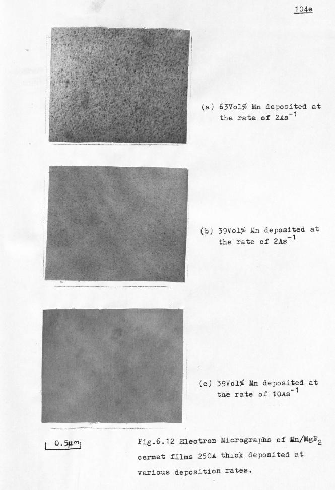
104e
(a) 63Vo1% Yin deposited at the rate of 2As-1
(b) 39Vol% Mn deposited at
the rate of 2As-I
(c) 39Vo1% Un deposited at the rate of 1OAs_1
I O. 5iv-j Fig. 6.12 Electron Micrographs of ß9n/ß+igF2
cermet films 250A thick deposited at
various deposition rates.

105
rates, the adsorbed atom are more mobile because thentime lag"
between successive impinging atoms is relatively long compared
with that for fast deposition. Hence the Mn islands in the pure
metallic films are large and their inter-island separation
(diffusion length) is also large resulting in high p
As the deposition rate is increased, the "time lag" is reduced,
thus reducing both surface mobility and the degree of agglomeration.
Hence the Mn island size becomes finer with smaller inter-island
spacings leading to a fall in p. Island growth in this case may
be due to collisions from evaporant atoms impinging on already
adsorbed atoms, as opposed to lateral growth in the case of films
deposited at low rates.
In the case of the cermet films, both Mn atoms and MgF2 mole-
cules execute random motion on the substrate at low deposition rates.
(Electron microscopic investigations indicate there is no chemical
reaction between Mn and MgF2 in the temperature range 290 to 455x).
The rate of agglomeration of Mn - Mn particles should therefore be
reduced. This would make the Mn island size in the cermet film
smaller than that for a corresponding pure Mn film. These island
should also be smaller because the amount of Mn in the cermet is
smaller than that in pure manganese films of the same thickness.
Another possible explanation for the fall in island size with
rise in deposition rate may be as follows:
(i) Neugebauer 89 postulated that for an inhomogeneous substrate,
a relatively high density of small islands is formed at

i06
(ii)
tight binding sites (valleys). He obtained support for his
hypothesis from Au films 96
deposited on rock salt. These
films indicated that a high density of smaller island are formed in the region of the "staircase" of cleavage. The
Mg? 2 atoms may therefore be thought of as making the
substrate less homogeneous to the impinging Mn atoms.
Campbell 100 observed that the tensile stress in UP films
deposited on mica increases with an increase in deposition
rate. For example the tensile stress of a film I000A
thick is 6x 10 14 Nm -2 at 6 As -1.9x 10
14 Nm -2 at 50As -1
and 12 x 101 4Nm -2 at 65A. Hence the increase in
)O with increase in deposition rate for Mß/ gF2 cermet
films may be due to the higher number of stresses present
assuming that stress - deposition rate characteristic of MgF2 and Li? are similar.
It was not possible to compare the present results (110gk'2)
with those of other workers as there appears to be an absence of
published data in this area. However in the case of pare metallic
films where some data are available, no clear pattern has emerged
for the relationship between deposition rate and film resistivity.
Learn and Spriggs 101 observed that the critical thickness
(i. e. thickness at which the film becomes structurally continuous)
of lead films deposited at 300K on crystalline quartz is constant
at 400A when the deposition rate is low 0.25 to 0.5As - 10
increases rapidly to a peak at 950A as the deposition rate is
increased to lAs - ý, and then falls rapidly with further increase
in deposition rate. If a structurally continuous film indicates a
low film resistivity (see Fig. 6.5) it follows that /D for the
lead film was probably constant between 0.25 and 0.5 As - 1, then

107
rose to a peak at iAs -1 before falling with further increase
in deposition rate. They also obtained a similar result for
tin films.
Fridrich and Kohout 97
have observed a decreasing agglomera-
tion with increase in deposition. rate for Aluminium films deposited
on ceramic substrates. The critical thickness in these films
occurred at 55A for a deposition rate of 6.6 As - 11,122A for
I . 3As -1 and 260A for 0.61. As - 1. These results suggest a
decrease in P with increase in deposition rate.
Adamov et al 98 found that the resistivity of sputtered and
vacuum-deposited Au films on Borosilicate glass was higher at low
deposition rates. For example, a thermally-evaporated film 600A
thick has a resistance of 5-a when deposited at 0.5As -1 and
3 Si when deposited at I As 1, The corresponding values for
sputtered films were respectively 2.5 S- and 1.5 -a "
The phenomena of decreasing agglomeration with increase in
deposition rate is- the most frequently observed in thin film
studies. Thun 94
has postulated that a minimum deposition rate
exists above which this phenomena will be observed and below which
agglomeration remains constant with decrease in deposition rate.
This is in agreement with results of Figure 6.8. His results for
Cr films I000A thick (Fig 6.13) also show that agglomeration
decreases with increase in substrate temperature, and at a substrate
temperature of about 300K the Cr island diameters were constant,
and independent of deposition rate from about 10 to 450 As - 1,
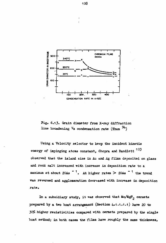
108
300
R
aiiiIII
340"C
CHROMIUM FILMS IOOOA
x z ir
2oo1C zoo vv- º- X_ ý 25"C v- <+ +- -+ . -
z ioo J ¢ 0
Ö01-'200. i-300i 40-0i
CONDENSATION RATE IN A/SEC
Fig. 6.13. Grain diameter from X-ray diffraction line broadening Vs condensation rate (Thun 94)
Using a Velocity selector to keep the incident kinetic
energy of impinging atoms constant, Chopra and Randlett 103
observed that the island size in Au and Ag films deposited on glass
and rock salt increased with increase in deposition rate to a
maximum at about 20As - 1. At higher rates > 20As -1 the trend
was reversed and agglomeration decreased with increase in deposition
rate.
In a subsidiary study, it was observed that Mn/Mg'2 cermets
prepared by a two boat arrangement (Section 1+. 1.1.1.1) have 20 to
30% higher resistivities compared with cermets prepared by the single
boat method; in both cases the films have roughly the same thickness,
x-x

1o9
composition, substrate material, and were prepared at about the
same residual gas pressure and substrate temperature. The only
difference between the two techniques being that with the single
boat system, the deposition rate was kept constant (Ms - 1) at
all cermet compositions whereas with the two boat system, the
deposition rate of one boat was varied with respect to the other
in order to obtain the required composition. However with pure
Mn, both techniques produced films whose resistivities agreed to
within ! 5% for the same deposition rate 4As - 1.
It was also observed that, the higher the deposition rate., the
more difficult it is to obtain repeatable readings. ýp values for
five separate runs at 50As -1 showed up to 50% deviation from the
mean value whilst a deviation of 5% and 17/Ov- were obtained at
2As 1 and 25As -1 respectively. Scratch tests on these films
also revealed that their hardness decreased with increase in deposi-
tion rate. Above 50As 1 it was possible to disrupt the film by
wiping it with a clean lens tissue.
These results show that:
(i) a higher film resistivity may be achieved in pure Mn films by decreasing the deposition rate but the reverse is true for MrAgF'2 cermet films;
(ii) a high degree of reproducibility may be achieved by depo-
siting Mn and ld4&gF2 cermet films at low rates (2 to 8As _1) ;
and
(iii) poor adherence of the film to substrate occurs at high deposition rates (> 50es I).

110
6.6. VARIATION OF RESISTIVITY WITH RESIDUAL GAS PRESSURE
When thin films are fabricated by vacuum-evaporation, the
chamber pressure is usually kept as low as possible in order to
reduce the degree of contamination. Contamination usually arises
from the interaction of the residual gases in the chamber with the
evaporant vapour and/or with the adsorbed evaporant atoms/molecules
at the substrate. Such contamination may alter the electrical and
structural properties of the film. In the present study, the effect
on the resistivity of Mn and Mn/'gF2 cermets of varying the pressure
of air and argon was investigated. Here the films were 250 and
500A thick and were prepared at a constant deposition rate (14FAs - 1)
on mica pre-coated with carbon and Corning 7059 glass substrates
held at 295K. The chamber pressure was varied from 5x10 -6 to
5x10 -4 -4 torr for air and 1x10 _5 to 5x10 torr for argon.
The results are presented in Figure 6.14 for the 250A films
and Figure 6.15 for the 500A films. For a given film composition
1C increases with increase in pressure. This increase is gradual
at first tending to saturate at around 5x10 -4 torr. With each gas
LA tends to increase as the insulator content increases. It LP
can also be seen that for a given composition, thickness and pressure,
the resistivity of films deposited in air is higher than those depo-
sited in argon. For example, with the 100% Mn films 250A thick,, p
is 900 pS2- - cm when the film is deposited in air at a residual
gas pressure of 5x10 -5 torr and 702 tom51 - cm when deposited in
argon, a fall of Pý, 22/. With the I0O5 Mn films 500A thick, depo-
sited at 5x10 5 tort, the corresponding fall in the resistivity

i0-1
10ýý
10
W
E .. ý M. Fr
ý
ý
- b-
ý
ý
P-
ý
r
W.
it 3-9fa19mn S 63tia2IWD Ai. r TI OO*a
O 34Yo19äiOt 0 b3VolOa © 1OQYo1ý
Argent
Depoaitioa Rate 4As`1 Depo$it3eaa ? aaperatare. 295K
I 0`4J r1,, 111
3z10-6 '10'5 10-4 7Z10 3
l? reasure/Torr
Fig. 6.14 R«tstivity Ys Pressure for in and IWXg72
fj't 250A thick

10-I. -
. -.
10-2
10-3
r
..
39rýo] 63ga1 a Air
V 1oO%M O 391o1%*n L7 63Vo1%M* Arg"
ioo%ita Depoaitioa Rate 4As Deposition Temperature 2952
10`4 1 ;t '--1 [if º L., _. I III JII -L-Jj
3z10-fi 10-5 10-4 7zi0-3 Pressure/Tarr
Fig. 6.15 Iesistivity Ws rrearssrs for Mn and
iEayfYgF2 Si2sa 500A thick.

111
of air deposited films was -%, 30%.
With cermet films, the fall in '0 appears to be larger.
For example, the 63 Vol % Mn cermet, 500A thick, and deposited at
5x10 -5 torn, has a resistivity in air of 580 - cm and 2440
f- cm in argon, a fall in 0 of about 60%.
The electron micrographs for the 100106 Mn air-deposited films
(Fig. 6.16) clearly shows that the size of Mn islands decreases as
the deposition pressure is increased.
As the chamber pressure is reduced, the number of residual air
molecules trapped in the vapour stream per unit time decreases.
Hence substrate contamination should decrease which implies that the
surface mobility of adsorbed Mn atoms increases. If we assume that
most of the vapour-gas collisions occur on the surface of the sub-
strate, this results in increased agglomeration and hence a lower
film resistivity. This assumption is not unreasonable if one consi-
ders that the m. f. p of air at 1x10 -4 torr is &, 50 cm at 295K, so
that the probability of forming oxide molecules through collisions
in the vapour phase will be very small. Instead collisions are
more likely to take place at the substrate surface which is exposed
to the evaporant and air molecules.
It is known 104., 105 however, that the oxidation of a metal surface
proceeds at particular nucleation sites and results in the formation
of a non-homogeneous oxide layer. The latter prevent surface diffu-
sion and so reduces agglomeration. The higher resistivity of air-
deposited films over the argon-deposited ones can probably be

111a
.. _-. -- ý--"ýý e. --. .-- ýfr ryi? y r
i'. ý. ., 9_ý'ý s L'
. eyýý., f_ý".
is' _ .r . '4iý `ýP`
,
Yý4: ýý"'ý ý'': `~' r, l`'ýý; ' f`.. ý''ýý", "ºt ýý. '". i: , ,, ýf"- tý,, ý"t,,, ý" ý r, . wý P4
'. ý. -'A 4, ,, 1 'J ' , t, ri , 1j"`0r I
<;. ýa" wv iý I 'r, f ly , I'+ '
, 'I ý
ýý , }.
.,
"ý'ý,, t ý'" ýý I *ýf
ý ý. 'ý
. fV . ilr.... ý
. `/_ 4_. ý+' w' Y
ý P. -f ,, tp"fý--r ! o6
t'j"'qý`; ý ý %ýt. ýrr(" ýia "ý ,
V,
, ,ý "}ý'ý yý , ý",: f3
ý'r ý' !I,
f Tk "ýi ý" 1, ý ýrv =ýýk},
aA r'1"' ýý{'ý/fý. r i- ', a.
. r_ ä. ý
.,
ý! ýýý: `t. 'd'. Ii'ti"'"., .
ý. ý,. ti
{. {ý'.
týýi.,,
, : -i'.:. ý; .. `.. ýti ý; i. ^. r",. '
.. ýýý .
ý. ý .. . ý"" s. TJ: Y'ý `" }
`-ý i"- * ý` "'ý
.ý.. Hs ý.
Iý RY ý
44 f4 -_ -_. __... f1
(a) 100q&n deposited at
1x10⁻⁵torr.
(b) 100j%IMln deposited at
1x10⁻⁴torr.
(c) 100Iün deposited at
5x10⁻⁴torr.
0. InFig. 6.16 Electron Micrographs of pure Mn films 250A thick deposited at
different air pressures.

112
accounted for in most part by oxidation although no definite
structure could be obtained using a transmission electron
diffraction technique.
6.7. HEAT - TREATMENT CF PURE Mn AND MiV 2 CERMET RIMS
The films used in this investigation were prepared by the
method described in Chapter 5. After fabrication the films were
transferred into the auxiliary vacuum plant (see Section 4.2.1)
and their temperature raised gradually at a rate of 4K min -1 from
about 295 to 620K. The film were held at the annealing temperature
for a period varying from 1 to 3 hours. Then the temperature of the
film was cycled between 620 and 110K. The film resistivity was
monitored throughout the heat treatment (annealing) and the tempera-
ture cycling operation (post-annealing).
Figure 6.17a is a schematic representation of the resistivity-
temperature graphs for both pure Mn and Mn/MgF2 cermets with thick- 6. i_Tb
nesses > 1000A whereas Figure represents those for Mn/MgF2
cermets < 500A. The graphs have been divided into two regions
A and B for convenience, depending on whether they show a reversible
or an irreversible change in resistivity with change in temperature.
6.7.1. ANNEALING
Figure 6.18 shows the actual resistivity variation with
annealing temperature for the 100% Mn, 63 Vol % Mn and 39 Vol % Mn
cermets of 500A thickness. These curves correspond to region A
in Figure 6.17.

112a
ta0
ý
31 oý ý ý ý
E_ý
ýý B (Reversible resietiTity
chý and ' positive 2(M)-
Tasperataý
(b)
m ý ao ý
B ( RArwarsiiPl* rem st%ity chaýge and mgatfTe TM)
tamtPeratair*
Fig. 6.17 swasatic representation of Seat
treat t of Ya aM 1(ßfxg72 'this fi2as

1A-ab
DepcsaitiaFa T. eapesatnre 295X Depositioa Bate 4As-1 j)epee&itiaa Pressure lsio-5torr
300 500 600
ag Temperature /g
Fig. 6.18 gesistLYity tos nnesi; g 2eaperature- tar lb~2 bins 500A tick.

113
Aire Mn films experience a fall in )O with rise in annealing
temperature. InitiallyýoO decreases very slowly from 312 t1. R - cm
at 295K to 305 f6l - cm at 410K, then more rapidly from 305 to
235 - cm between 410 and 575K and finally drops off again
beyond 575K.
The resistivity of the cermet films can be seen to decrease
rapidly as the annealing temperature is increased, the decrease
being most rapid between about 400 and 500K. However the fall is
steeper in the 39 Vol % Mn films than in the 63 Vol % Mn. Similarly
the fall in the 63 Vol % Mn films is steeper than that for the 100jä Mn.
A similar decrease in/0 was obtained with films deposited at
elevated substrate temperatures (295 to 1+55K) (see Section 6.4).
The important difference between the two experiments being that films
deposited at elevated substrate temperatures (Fig. 6.6) have a lower
resistivity than those annealed at a higher temperature (see Table
6.6).
The fall in /O with increase in the annealing temperatures is
usually attributed to the removal of structural defects incorporated
into the film during growth, as this process is irreversible. The
result in Figure 6.18 suggests that the number of structural defects
in the films increases as the MgF2 content increases. Like films
deposited at elevated temperatures (Fig. 6.6), these films (Fig. 6.18)
exhibit a less steeper fall in P with increase in film thickness.

114
ý'Y ý2 "
An? fIºA II i sýg 2
ýý 'ý )LA " Ci )
Co$poai t, iaa . or Film-19 cl-epos - Filar depoa -
{rol. % Mn ) depoaiticn ited at 2955 ited at temperature aýä then elevated
(Y) anaseale. d temperature
295 315 312 100 350 250 312
400 176 306 455 1510 288
295 490 450 350 425 425
63 4.00 365 388 455 315 370
295 825 800 350 6.20 775
39 . 400 500 700 455 475 550
Table 6.6. Resistivity of Mn and MXV/kgp 2
film
500A thick, deposited at 295K and then annealed
compared with that for films deposited at elevated temperatures.

115
As we have seen in Section 6.4, an increase in substrate
temperature may lead to an increase in agglomeration. This may
account for part of the observed fall in p. The electron micro-
graphs in Figure 6.19 show that there was a considerable mass
transfer in both pure Mn and Mr gF2 cermets of 250A thickness,
annealed at 620K for 1 hour.
Vard 106 has also given an explanation for the fall in resis-
tivity of metallic films with annealing temperatures. In the next
section, an attempt is made to interprete the fall in p of pure
Mn films in terms of his theory.
6.7.1.1. VAND' S THEORY 106 OF THE EFT =T OF ANNEALING ON RESISTIVITY
According to Vand, the defects incorporated in Vacuum-evapora-
ted metallic films lattice distortions, are a "combined type"consisting
of vacancies and interstitials in close proximity to one another. He
assumed that a characteristic energy E is required to allow the defects
to combine and cancel out but that the energy required to bring about
the migration of these defects towards each other is negligible.
If r (E) is the contribution to the residual resistivity made
by one distortion per unit volume, No (E) the initial number of dis-
tortion per unit volume (i. e. at time s= o) and 0 (E) AE is the
number of distortions per unit volume that have decay energy between
E and E+QE, then the total contribution to the film resistivity
P due to imperfections is given by:
00 r (E) N (E) as
: S_. _

(a) 06) 1 15a
(c. )
10 0%Min before annealing
(d)
39Vol%Mn j "41 before annealing
1 oo%Mn after annealing
39Vo1%Mn after annealing
Fig. 6.19 Electron Micrograph of Mn and Mn/MgF2 films
25OA thick before annealing and after annealing
at 620K for one hour.

116
The distribution function F0 (E) describing the energy spectrum
of the distortions in the film is given as:
F0 (E) =r (E) N (E) (6 - 2)
A complete analysis of equations (6 - 1) and (6 - 2) gives:
Fo (E) = ýkU' 1
di TJ 1 (6 - 3)
where aP is the slope of the resistivity Vs temperature graph when. dT
the temperature of the film is raised at a uniform rate and the resis-
tivity is measured as a function of temperature, and therefore of time,
k is Boltzmann's constant and U is defined by:
U=u (u+ 2 u+1
where:
(6 - 4)
u+ log u= log 4- ns vmax (6 - 5)
and n is the number of atoms that can initiate a defect (this
number is unknown but it is estimated 106 to be s* 10), V, is the
characteristic maximum vibrational frequency for the lattice assumed
to be the same for the distorted lattice of a metallic film and s is
the time for the film to reach the particular temperature at which
dR is measured. u is obtained by successive approximation of dT
equation (6 - 5) so that F0 (E) may be plotted against E (= uk T) to
give the lattice distortion spectrum.
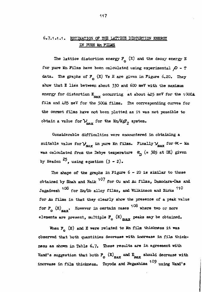
117
6.7.1.1.1. ESTIMATION CP THE LATTICE DISTORTION ENERGY
IN PURE Mn FILMS
The lattice distortion energy F0 (E) and the decay energy E
for pure Mn Films have been calculated using experimental P-T
data. The graphs of F0 (E) Vs E are given in Figure 6.20. They
show that E lies between about 330 and 600 meV with the maximum
energy for distortion Emax occurring at about 425 meV for the IOOOA
film and 485 meV for the 500A films. The corresponding curves for
the cermet films have not been plotted as it was not possible to
obtain a value for') for the Mn, /4-P2 system.
Considerable difficulties were encountered in obtaining a
suitable value fort/ in pure Mn films. Finally'11 for 0C- Mn max
was calculated from the Debye temperature @D (= 385 at OK) given
by Meaden 25, using equation (3 - 2).
The shape of the graphs in Figure 6- 20 is similar to those
obtained by Shah and Naik 107 for Cu and Au films, Damodara-Das and
Jagadeesh 108 for. Srj/Sb alloy films, and Wilkinson and Birks 110
for Au films in that they clearly show the presence of a peak value
for Po (E)max. However in certain cases 108
where two or more
elements are present, multiple F0 (E)Max peaks may be obtained.
When F. (E) and E were related to Mn film thickness it was
observed that both quantities decrease with increase in film thick-
ness as shown in Table 6.7. These results are in agreement with
Vend's suggestion that both Po (E) and max should decrease with max increase in film thickness. Toyoda and Negashima log
using Vand's

1
ý ý
A' o
W %-. 0
o 400 94
300
200
100
600
._
M.
MBub
a-
A 1 I
250 3S0 450 Z/ »9
550
Fia. 6.20 Iiýc: or asatort&aa. _7 (3) vs DsaaT gy (S )
0

118
i FilJR thiclmess
ýgý
250 500
1000
Table 6.7. Variation of FO (E)Max and Fmax
with Mn film thickness.
theory on carbon films also found a similar thickness dependence.
In their case Fo (E)Max for 110A films occurred at 2.3 eV and at
1.6 eV for the 380A films. On the contrary, Wilkinson and Birks 110
with Au films found that Fo (E)max was independent of thickness
over the range 100 to 900A for a constant deposition rate. (The
deposition rate was not given but it is assumed to lie between 0 and
595 ) cm -2 min 1). However they observed that F0 (E)
max does
increase with increase in deposition rate, thus indicating that Au
films prepared at lower deposition rates have fewer structural
defects.

11 9
Toyoda and Nagashima log explained that the fall in resis-
tivity during annealing may be due to imperfections being die-
placed into regular lattice sites. An alternative explanation by
Haffman et al 111
assumes that:
(i)
(ii)
the number of vacancies in the film far exceeds the
equilibrium value; and
that during annealing the vacancies coalesce to form
progressively larger groups until they finally arrange
themselves into sheets and collapse to form dislocation
rings. They supported this hypothesis with results from
strain measurements on nichrome films in the process of
being annealed. The volume change corresponded fairly
closely with observed resistivity change.
6.7.2. POST ANNEALING HEAT- TREATI ENT
The results for the post-annealing heat-treatment of Mn and
Mr; /MgF2 cermet films (250,500, and I000A thick) are presented in
Figures 6.21,6.22,6.23 and 6.24.. The resistivities of all the
films investigated were found to be completely reversible at all
temperatures below. the maximum annealing temperature (i. e. no hys-
terisis was observed), and irreversible above this temperature.
These correspond to the reversible region- B in Figure 6.17.
Figure 6.21 for the 100/ Mn films shows that after annealing at
620K for 1 hour, the resistivity of all films ). 25QL increases with
increase in temperature and vice versa during the following tempera-
ture cycling (110 to 620K) (i. e. the films have a positive TOR).
This is an indication that the films have become structurally conti-
nuous. The electron micrographs Figure 6.19 for the thinnest of these

.ö
L .. 01 v
400
ý b M ý m
ýi m
Cýi
300
200
-
ti
ý
P--
..
Pý
ý
100 I-
0135? ? sspera#ýsre /1 o2iC
Fig. 6.21 Ye. a, ¬atIvity Ta 2mpasatsre far 100%Mn filss
aassaasd at 62oiC law i Low.
J. 4 4 4

0 11=ealed at 690Y for 3 boars XAnma ied at 7 2DrS for I hour
450,
``-- I CA ý
Q1, v
ý 350 -rq a *rq 42
250
-
ti
540A
150
I i
1246
Tespessture / i02Y
6.22 iLesiatirity Ys Tomps=ture far
100%iia itilas.
!1 . rý ý.
4
$

I 191
700
s u
c ýý
600
500
400
300
ý
k-
..
..
ý
JI
25-OA
50OA
ýI 0135
ýeýnpera#ýxrs / 102K
7
2ig. 6.23 iieaistivity ire. ftspsratarQ for 39Yo196MnfW2 Comsat =no anneaSad at 6.2QK for 1 hour.

X 43Yo19ý/ý2 5,9gol%t*, /ftr2 54go1%itn/SiD 49tfo1%Cs/SriO
Ann "I I ng time 3 haare at f-9OI
380
". ý
300
220
140
mb
dº
Mº
ow
Mn/MgF2
Ga/mgF2
60 L------:
- II
03 -5 2=]Parat=, w / 102Y
Fig. 6.24 jjsa, tatiTity Va tmffpesatnre ior 5401
Coewet FS1, s.
119d

120
films (250A) confirms that they have indeed become structurally
continuous. Figure 6.19a shows the presence of Mn islands
prior to annealing, typical of a discontinuous film. Figure 6.19b
shows that the islands have grown laterally with the larger islands
touching to create continuous Mn paths throughout the film. Although
no electron micrographs were taken for the thicker Mn films. (500
and I000A), the presence of a positive TCR suggests that they must
also be structurally continuous.
The Mn films of 1000A thickness exhibit a practically linear
relation between jO and T. The resistivity increases only by
20 fLS2- cm between 110 and 620K, a percentage increase of about
15%c. From data presented by Meaden 25 (Fig. 6.25), the change in
resistivity for high - purity annealed bulk Mn is + 131"o, being
123 Ji. 2 - cm at 50K and 139
i- cm at 295K. Figure 6.25 clearly
shows that the temperature variation of the resistivity in bulk Mn
is considerably smaller than that for Cr, Cu andAu whose resisti-
vities increased by between one and two orders of magnitude.
The thinner Mn films of 250 and 500A thickness have a non-
linear P-T characteristics (Fig. 6.21) when the films are
annealed at 620K for 1 hour. It can be seen that between 300 and
450K, the resistivity appears to be constant. This may be a conse-
quence of incomplete anneaiý ing, as a similar result was not observed
in films annealed for 3 hours at 690K or at 720K for 1 hour (Fig.
6.22). This plateau region has been interpreted by a number of
workers 112 - 115 in terms of incomplete ordering.
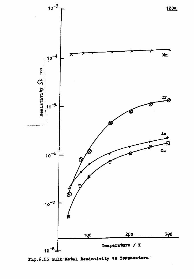
10-a
, ý Ck' , ý
10`5 äi
106
10-7
ý
0-
ý
1Q0
10`8-1-
2, Po
Taat perata» /1
Mn
no
Zig . 6.25, Bu]. t -Ysta1 lssistiTitW Ts Te*ps*atu=a

121
The P-T characteristics for the 39 Vol % Mn cermet films
annealed at 620K for one hour are presented in Figure 6.23. Here
the 250 and 500A films have smaller plateau regions ("v 1000) and
a negative TCR whilst the I000A film has a positive TCR. As with
pure Mn films, the plateau was not observed in cermet films
annealed at 690K for 3 hours and at 720K for 1 hour. This varia-
tion of TCR with thickness is an interesting result because it
indicates that when Mr; /MgF2 cermets are annealed at 620K for 1 hour,
the sign of the TCR is dependent on the film thickness, and on the
amount of Mn in the film. A similar result was obtained for the
63 Vol % Mn cermet films.
It is evident from Figure 6. i9b that a considerable amount of
mass movement of Mn particles occurs during the annealing process.
A similar migration of Mn particles also occurred in the cermet
films N 250A thick (Fig 6.19d) but to a lesser degree so that the
film remained discontinuous after annealing. No electron micro-
graphs were obtained for the 1000A cermets but it is assumed that
on annealing, the quantity of Mn atoms and their dispersal within
the fabricated films were sufficient to produce a network of con-
ducting paths.
Small variations in resistivity with temperature were observed
in all annealed Mnl*'ýMgF2 cermet films. Auxiliary investigations were
carried out to compare Mn and Cu oermets, using MgF2 and SiO as
insulators in order to attempt to establish the reason for the small
resistivity variations with temperature in MrVMgF2 cermet films.
The results are presented in Figure 6.21+.. The films contained

122
between 37 and 51 Vol % insulator (corresponding to 80 Wt %
metal/20 Wt % insulator), 500A thick and were annealed at 690K
for 3 hours.
The Mz gF2 system has the largest resistivity after annealing
but the subsequent variation in resistivity with temperature (110
to 690K) was the smallest being ru 40 jjSj- cm. That is, the value
of p at 690K increased by about 14$c at 110K. Between these tempe-
rature limits, the corresponding increase in p for Cu/UgF2, Mn, /
SiO and Cu/SiO are respectively 35/x, 46% and 91%.
From these results (Fig 6.214. ) it appears that:
(i) MgF2 cermets have a higher p than Si0 cermets although the variation of P with T in the former is smaller (11+ and 35%) compared with the latter (14.6 and 91%v);
(ii) Mz; /SiO cermets have a smaller variation of p with T (14.6 %)
compared with Cu/SiO (9j%);
(iii) a combination of Mn and hgF2 produced films of high D which
is only slightly affected by variations in temperature. Hence
the small resistivity variation with temperature in the Dam/
MgF2 system appears to be both Mn and MgF2 dependent with
neither component showing a distinct dominance. However
further work is necessary using more Mn and Cu cermet compo-
sitions and other metals to test these conclusions.
It also appears that the use of Si0 as an insulator reduces
the resistivity of Mn, /SiO and Ou/SiO to within the same order of
magnitude. This is interesting because in a limited way it gives
support to Neugebauer's hypothesis 66
that one curve can be used to
describe the resistivity of all metal/SiO system as the Si0 content

123
in the film is reduced, regardless of the type of metal used
or other deposition parameters. However cermet films containing
kg'2 do not appear to have this property. This is consistent
with the resistivity - composition results for KOgF2 cermets
presented in Section 6.2.
Let us now examine more closely the activation energy of
both annealed and unannealed g''2 cermets.
0.7"2.1 . ACTIVATION EI4, RGY CFUh'6MEAtMhin/%'pF2 CEI3tsSETB
Three film compositions of 1001 Mn, 63 Vol % Mn and 39 Vol
Mn were investigated. Their thicknesses were between 250 and 1500A.
'The substrate temperature was 2958 during deposition and no high
temperature annealing was carried out. The activation energy was
estimated between 110 and 2955 from the variation of In P with T-1
(see Fig. 6.26). Figure 6.27 shows the variation of activation
energy with thickness.
Figure 6.26 shows that the in p Vs T-1 graphs are linear for
all the film thicknesses indicated. However the I000A thick films
for i00j Mn and the 63 Vol Mn were non-thermally activated; the
are not shown in the diagram. Figure 6.26 also indicates that the activation energy increases with decrease in Mn concentra- tion but decreases with film thickness. The latter is more clearly seen in Figure 6.27. The activation energy decreased rapidly from 74.5 meV at 250A thickness to 10.4 at 1000A, and then more slowly to 7.1meV at 1500A.
A comparison of the activation energies of films of 250A thickness obtained from resistivity measurements (Fig. 6.26)
with those calculated using data collected from electron microcopy ( Table 6.2 ) shows that the former are about 30 to 35 % lower
.. However when the xX. xxxXxXXXX3; XXxxxxXX_: x. Xyx

123a
333
-1
Qý
0.
a ri
-3
-5
I-
ý
200 Tfitaperaturo (T) /g
1tL? ,,,
1 o0%ün Actiration Energy Q6 3Bai%l[n r 250A (MOT) X 39TaI%mn x 74.5
D1 oo%Nn 5aaA f 397o1! %län
ý
0 39To1%In 1000A
3.7
-9 i
3S7
10-3 =-1
Fig.. 6.26 lap ga T-1 . tos In and X"%'2 filna
doposited at 295Y (mmmealed)
1 9

k5r i mý ýý
E53,
ý ý ! 60 ý
F
40
20
0
-
ý. 0
I
0 500
I
1000
I
1500
Fits ThLakn. as /A
Jig. 6. a? Activation gy Vs Film Thickmsss
for the 39TOI% n/ g872 cermets deposited at 295K. Activation Easrgy
is measured between 110 and 295K.

124
error limits in the microscopic measurements are taken into
account the difference between the two values is less than
14�4 Hence the two sets of activation energies are in reasonable
agreement with each other.
This shows conclusively that between 110 and 295K, Neugebauer
and Webb's theory (Section 3.3.1) appears to be applicable to 38
all unannealed Mn films and MgF2 cermets of 250A thickness when
deposited at 295K. Hence electronic conduction is probably by a
thermally - activated tunnelling of electrons between the metallic
islands. Although there are no electron micrographs to give a
direct comparison, it is assumed that the conduction mechanism in
all the 500A and the I000A film with 39 Vol % Mn is also by thermally
activated tunnelling because of the linear relationship between lnic
and T in the same temperature range.
6.7.2.2. ACTIVATION ENERGY CF FILt. ANNEALED AT 620.690 and 720K
Figures 6.28 and 6.29 show the variation of In /- with T-
for annealed cermet films of 250 and 500A thickness. The 1000A
cermet films and all pure Un films have not been included as both
are non-activated and metallic conduction prevails (see Figs. 6.21
and 6.23).
Figures 6.28 and 6.29 show that there appears to be a spectrum
of activation energies. Hence the activation energy values shown
in the figures merely demonstrate an order of magnitude. However
Figure 6.28 indicates the presence of three distinct regions for
the 250 and 500A films annealed at 620K for one hour: a high tempera-
ture region, a low temperature region and a transition region, the

Temperature (T) /I 1000 333 200 142 111
-7.2
-7.4
-7.6
-7.8
-8-0
1
ý
._
ý
ý
p 250.2 5L5 annealed at 620 for lhr.
" 250,1 annealed at 690L fox Ara.
X 500A annealed at 720ä for ihr.
2.2 say
I I
5? s'ý / 10-3 S
1 I
Fig. 6.28 in P Ta T itor 39yo1%in / ý2 Cermeta

týb
Temperatnrt (T) /Y 1000 313
-7.6'
-8.0 i
Qý. i
FS r-q
f
1.18meV
-8.4
-8.8
_g
W.
)( b3go1%lb~2 Q 59Yo19GCU/Xg. T2 ý 49'go1%Cv, /S, iD ® 54Vo1%KYnfS3Q
1.3meT
13 5 79 T-s/ io-3 Y-1
Fig. 6.29 lap Ta T`4 Zar Carnet Films of 5001
thickness annealed at 694[ for 3 hogs.

13 m...,..,, e+.,,. _ i41 ä/ v-
ýý
.. i..
_ L. == 400 1
kPW+. AM. r. u jIA.
222 154 1-_ ---I
117 _.
3.
-0 25
ý
12
-0 0
ýý
11
x . ln. /Sio 2 min or et ul(bz
"AztYd/SM Tick et &1 117
10 ! -ý-=1-.. _ II-1
1.5 2.5 . ý. 5 6.5
T-ýý1o-3 11 -1
ý
.0
ü ý
ari ý ü
P4 ý ä!
q r9
+9
ý
21
20
8.5
23
Fig. 6.3p la Sheet Rssiatýtaaý Fs ý1 faý different csraets

125
latter corresponding to the plateaux in Figure 6.23. The low
and high temperature activation energy regions are also evident
in similar films annealed at 690 and 720K.
For a given film thickness the activation energy for the low
temperature region is lower than that for the high temperature
region as indicated in Figure 6.28. It can also be seen from this
figure that the activation energies in both temperature regions
decreased as the cermet thickness increases. This is in agreement
with the unannealed results.
Figure 6.29 shows that there also exists a spectrum of acti-
vation energies for the 63 Vol % Mn cermets (of 500A thickness
annealed at 690K for 3 hour) and other cermets investigated; viz:
59 Vol % 0u/149'2' 49 Vol % Cu/SiO and 54. Vol % MrVSiO.
It is interesting to note that similar spectra of activation
energies have been observed by many authors 45,62,116,117 for
different cermet systems as shown in Figure 6.30. For example
Sashital and Pakswer 116 obtained 3 different activation energy
regions of 12.9,8.6 and 3.4 meV for Au/Ta2O5 in the temperature
range 93 to 433K. It is more likely however that their lmýp Vs
T1 graph is a continuous curve rather than three distinctly
separate regions.
On the contrary McMaster and Fuschill. o 112
obtained a single
activation energy of 60 meV for co-evaporated 15 Vol % AuAiO
cermets deposited on Si02 substrates in the temperature range 300
to 873K. Extensive precipitation of Au in the cermet was also

126
reported by these authors after annealing at 8735. No low
temperature results were reported.
Tick and Fehiner 117 (Fig. 6.30) observed two activation
energy regions of 8 meV (low temperature) and 200 meV (high tempera-
ture) for Au - B3. - SiO composite_. films with the transition
occurring at 233K. Miller and Shirn 62
with Au/5i02 observed a
gradual increase in activation energy from 24.6 meV at 111K to
277 meV at 423K with the knee of the curve occurring at about 290K.
It is interesting to note that the transition from low to high
temperature activation energy occurs below 400K.
The origin of the high and low temperature dependent conduction
processes is not known. Tick and Fehlner 117 suggested that the
conduction process is dominated at low temperature by closely-spaced
gold-rich islands and at high temperatures by activated tunnelling
between the palladium - rich islands, On the other hand Sashital
and. Pakswer 116 proposed that the conduction mechanism may be due to
electron tunnelling between metallic islands; thexmionic emission of
charge carriers; and electronic conduction through trapping levels
in the different temperature regions. They assumed that these
processes may operate either individually or jointly but they were
unable to describe the exact relationship between the various pro-
cesses and the three activation energy regions in Figure 6.30.
In their paper Miller and Shirrs presented the low temperature
(< 300K) activation energy only, but by using their quoted resis-
tivity values, a spectrum of activation energies may be obtained as
indicated by the curve in Figure 6.30. According to these authors..

127
resistivities in the low temperature region should vary linearly
with temperature. They explained that conduction in this region
was due to thermally - activated charge carriers from the 8u
region tunnelling through the intervening SiO 2 matrix; the process
being analogous to conduction in discontinuous metallic films 38.
Van Steensel 45 obtained a non-linear relation between P and
T for Au films. In one example he obtained a low temperature ineV
activation energy of 44 and a high temperature value of 140 meV.
He found that his results were best interpreted by thermionic
emission of charge carriers. He explained that at high temperatures
the larger inter-island spacings (corresponding to higher energy
barriers) start to contribute significantly to the conduction
process. Hence the difference between the high and low activation
energies observed in cermet films may be due to the dielectric
making a significant contribution to the activation process at high
temperatures.
6.7.23 ELECTRONIC CONDUCTION NECiiANISM IN ANNEATZD
ýsF2 CERMETS
From the literature review of Chapter 3, it appears that
there are two main ways in which the resistivity of annealed
Mn/MgF2 cermets may depend on temperature, viz p co<exp (T - 1)
and p c)-d, ' exp (T 3). In either case the film is considered
to be composed of isolated metallic islands separated by dielec-
trzco
Both Figures 6.28 and 6.29 as well as the In ft Vs T
graph of Figure 6.31 indicate that conduction in }Qzv%g? 2 cermets

127a
-7.2
ql -7.6
-8.0
-8.4
2imperatare (T) /t
: 1100 625 27Z 156
V
h-
ý
..
Xý
© 39Vol%iEa amealod at 620[111ar. ""ý 69=131wo. Fl ." 620Y f 1ýir.
ý' 63ýa1ý " © 59Tc 1%Cn
0 6w3irs. T20IL/1ir. 69tK/3kro.
250A
8 34 ral L4 ! 10-2 L4
Yig. 6.31 in p TO s4 Zar Yeta1/YgF2 000010
100 T
10

128
do not occur by a single thermally - activated mechanism. The
interesting feature of these graphs is that the activation
energy of all 50QA films have low values as . have those within the
low temperature region of the 250A cermets (0.80 to 5.80 meV).
It is interesting to note that a low activation energy of
about 4 meV (E .N0 120) was obtained (between 35 and 300K) by
Abeles et al 63
for Auy/A12 03 cermet films containing 38 Vol jo Au.
This composition is also close to the transition composition
(about 40 Vol % Au) for this cermet. According to these authors,
conduction in the dielectric regime occurs by thermally - acti-
vated tunnelling with a charging energy E (see Section 3.1.3),
and in the transition regime by percolation, /thermally - activated
tunnelling.
The electron micrographs of MnyMgF2 cermets in Figure 6.19
show that the films are composed of isolated Mn islands and a
Mn metallic-maze structure. These films have a negative TCR which
is contrary to the positive TCR obtained in the metallic regime
but typical of those cermets in the transitional and dielectric
regimes. (Hence the films are either in the dielectric or transi-
tional regime).
Films in the dielectric regime are field dependent 63
( 1np or F-1, where F is the electric field strength) and
frequency dependent 63,118 (1 np cK f-1, where f is thv
frequency). Also films in this region show a linear relationship
between lnp and T1 or 7 - ý.

129
Mo'2 cermets of 250 and 500A thickness and annealed at 620,
690 and 720K are ohmic, frequency independent (100 Hz to 18kHz)
-1 and lnýp neither varies linearly with T nor T-' in the
temperature range (110 to 720K). Therefore these films probably
lie within the transition regime.
At low temperature, electronic conduction in annealed
Mn%MgF2 cermets is primarily a percolation process and at high
temperatures, the process is boosted by electron tunnelling
between isolated Mn islands.
Figure 6.19 shows that the annealing causes the agglomeration
of Mn lislands in the film. Compared with the 250A thick films,
it is likely that the 500A cermets contain a relatively larger
number of Mn percolation paths than isolated Mn islands. The con-
duction process is dominated by electrons percolating along the
maze structure at all temperatures from 110 to 720K. Such a mecha-
nism could be responsible for the low values of the activation
energy.
In the case of the 250A annealed cermets there are fewer
percolation paths but the number of isolated Mn islands increases.
In addition, in order for the cermet composition to remain fixed
separation between Mn islands must increase. Therefore percolation
conduction is reduced and thermally - activated tunnelling is
enhanced at high temperatures. Then the 250A cermets should have
a higher activation energy than the 500A, which is in agreement
with experimental results.

130
At low temperature, due to the relatively large inter-island
separations and the low thermal energies of the electrons, the
percolation currents far exceed the tunnelling currents. In this
region, the activation energy is low (^- 0.9 to 1.8 meV, Fig. 6.28).
Thus giving further support to a percolation dominated conduction
process.
The activation energies for the high temperature region are
higher (-- 18 to 45 meV) than those for the low temperature region.
Here it is likely that the thermally - activated tunnelling process
contributes significantly to the conduction mechanism.
The tunnelling process may occur in two stages owing to the
relatively large inter-island spacings. An electron may tunnel
firstly into a trap level in the dielectric MgF2; tunnelling into
the next metallic island from this trap level is not possible as
there are no empty states at that level. The electron must hop
into a higher trap level in Mg? 2 where tunnelling into the next
Mn island is possible. Transitions from isolated Mn islands into
Mn metallic maze is also possible.
6.7.2.4 TEMPERATURE CCEFF'ICIENT OF RESISTIVITZ (TCR)
MgF2
Figures 6.32 and 6.33 show the variation of TCR with Mn, /
cermet composition for both . unannealed and annealed films
deposited at 295K. The TCR was also measured at 295K.
Figure 6.32 for the unannealed films shows that the 100% Mn
films of I000A thickness have a positive TCR. -.. + 500 ppm K'
whereas the cermet films have a negative TCR.

pig-6.32 TCät 9n #ta/l[gF2 Cerset Coap©siti"
aeasursd at 295= for tilas de posi ted
at 295X (un=w&2ed)

400 MW
ýý_ 200
ht'i
ý P4 i i J0
-200
-400
-6001- 100
I
so
I
60
TOl%ft
: OOQA
4
250A
40 30
ü6.6.33 TCR Ta 2 Gerast Coapoaition for Fits
d: poaited at 295K and a mealed at 620K for Ihr.

131
For a given composition the TCR increases in a negative
direction as film thickness decreases. It can be seen that only
1000A thick pure Mn and 60 to 90 Vol % Mn films have a TCR lying
within the commercially acceptable range 57
of TCR's, viz: - 250
_1 to + 250 ppmK.
Figure 6.33 shows the corresponding graphs for films deposited
at 295K and then annealed at 620K for one hour. Figure 6.33 is
similar to Figure 6.32 in that it also shows a negative increase
in TCR with a fall in both film thickness and Vol % Mn. These
properties imply that TCR increases with decrease in resistivity
since an increase in the insulator content of a cermet film genera-
lly leads to an increase in its resistivity. Indeed a number of
workers 57,119,121 , 122 have found this to be the case.
- "gF2 cermets, 250A thick exhibit a small positive TOR for
metal content > about 90 Vol %o Mn. On increasing the thickness
to 500A we find that the positive TCR region extends from 100 to
about 72 Vol % Mn, whilst for thicknesses . 1000A the TCR is
always positive, at least in the range 100 to 39 Vol % Mn.
It is interesting to note that most annealed films are either
within the commercial range or very close to it except for the
250A films with Mn content less than 55 Vol %.
6.8. RELIABn. Tmv OF MV/%g"2 CERMETs
The reliability of an electronic component is usually based
on three criteria:
(i) performance;

132
(ii) stability; and
(iii) production cost.
Unfortunately, these three factors often interact with one
another, thus making it difficult to assign a reliability rating
to thin film resistors. Production cost is outside the scope of
this thesis. Experimental results of the performance and stability
of Mn and Mn/. VgF2 cermets are presented in the following sections.
6.8,1 Piwomump
Figure 6.34 shows the current-voltage characteristics of Mn
aryl MdgF2 cermets of 500A thickness. The films were deposited
on Corning 7059 glass substrates held at 375K and they contained
between 10 and 100 Vol % V, n. The electrical resistivity measure-
ments were carried out in air at room temperature.
All the films investigated exhibit a linear current-voltage
(I - V) characteristics up to the break-down point where the film
burnt-out. The power handling ability, of the films is good,
being 3kWm-2
A linear I-V relation was also obtained for measurements
carried out in vacuo. The break-down voltage and the resistor
handling power were of the same order of magnitude. However when
the resistors were operated continuously at 75% of the break-down
voltage (75% was chosen arbitrarily), it was found that their
value increased very rapidly in air to within 2 to 3 times the
initial value in 3 hours. Resistors in vacuo showed an increase in
resistance of less than 2501'o in 48 hours.

132a
0
I
SYMBOL
x
V
us
OD
i ýF= VoLAb
-
100
63
39
22
10
mayi}mim Power
30
30
33
28
36 I
20 40 Vol tage /T
Sheet [Re sistance
sz/Q 22.7
52.1
83.3
214.2.
781.2
Ifig. 6.34 Qur"mt-gal. taas characteriatic of
Xzoggy2 ccztets weasssýed in ais . i'ie
Yi2aa were 25" thick and me"
deposited at 375t

133
When the substrate temperature of the cermets in vacuo
was raised to 375K, it was found that the break-down voltage
decreased by-%o2O. A possible explanation for the lower break-
down voltage may be that the substrate acts as a heat sink and its
effectiveness diminishes when its temperature was raised.
6.8.2 STABILITY
The stability of a resistor should be determined by the
maximum drift in its value during its entire life when operated at
certain specified conditions (such as operating temperature, power
handling,, relative humidity etc. ) As this would involve tests
lasting for many years and high costs, stability data are usually
obtained from thermally accelerated aging processes. These pro-
cesses usually involve subjecting a test resistor to a constant
hi temperature for about 1000 hours 93,123. high In some cases a
voltage is applied across the resistor during the aging process.
Unfortunately, there were no facilities for carrying out the
thermally accelerated aging process. Instead some resistors were
stored at room temperature and atmospheric pressure, and some at
room temperature, and a residual air pressure.., I x10 -1 torr. The
film resistivities were measured at regular interval of time over
a period of six months. The results are presented in Figure 6.35,
for both annealed and unannealed cermet films of 250A containing
39 Vol % Mn.
Figure 6.35 shows that /0 varies almost linearly with
logarithm of time for films stored at I X10 'torn; the change

10 'COZ 't03 Tiowlirs 104
! ̀ ig. 6,55 Alf - Var-Time for asoIIoaSeek and monowIted 39vo1% Ma Cesmets stsaed at
p roam Temperature/ tz? etorr
and at room Tomperature , _.. rý .... _ ..
/Presswo
Imm
40
30
70
r.
W-
2501 Cerasts ato'ed at roos tempesatnrsend presanra
0 4
10 102 Time ! hm.
1Y6.6.36 AP_ Ya TiM for 3Wa% Na Cmmm*s xith daffldtioa rats 33 a
1` pareaster.

133b (a) 0.5pm
(b) ý' ý
(c) ;; . 5µm
on deposition day
after 720 hours
after 4,300 hours
Fig. 6.37 Electron Micrographs/Diffraction patterns for
39Vo1. %Mn/Mg1'2 fi1n 250A thick stored at room temperature
and pressure.

131+
being from 0 to 2C and 0 to 14 respectively for the unaxuiealed
and annealed films in 4,300 hours. However when the films were
stored in air over the same period of time, the corresponding rise
in are 30% and 70jb respectively.
Visual observations show that after about 1700 hours, a large
number of randomly distributed transparent spots (- 0.1 mm diameter)
were visible in the films. These spots grew progressively larger
in size, and new ones forming in the spaces between the larger spots
until the whole film became transparent after about 6,500 hours and
the film resistivity became infinite.
The electron micrographs of the unannealed, 39 Vol % Mn
cermet films stored at room temperature and atmospheric pressure are
shown in Figure 6.. 37. Figure 6.37(a) shows the structure of the film
immediately after deposition, and Figures 6.37(b) and 6.37(c) the
structure of the same film after 720 and 4,300 hours.
It can be seen (Fig. 6.37 (b)) that after 720 hours in air, Channels are prese nt in ire 4if ms . 71,, ese. channels are in fact regions of intensive oxidation (Mn 02 pyrolu-
site was identified). This tends to support the hypothesis 10lß., 105
that oxidation proceeds at particular nucleation sites. The channels
grow larger and larger in size until they become inter-connected.
This marks the beginning of the steep rise in graph of Figure
6.35. As the channels grow it appears that the unoxidized Mn in the
film migrates thus leading to agglomeration and a higher concentra-
tion of Mn. The effect of this migration can be seen in Figure
6.3? (c)

135
Figure 6.36 shows the variation of with time at two
different deposition rates. The graphs show that P
of films
deposited at 2 As are less affected by oxidation when compared
with those deposited at 25As 1. The percentage difference in
resistivity between the two films being 5,12 and 22o respectively
after 24,72, and 720 hours. A possible explanation of this
difference may be due to the structural characteristics of the films.
Films deposited at 25As have a finer grain structure than a
corresponding film deposited at 2As - 1. Hence Mn in the latter
will have a smaller surface area exposed to oxidation and conse-
quently a smaller rise in LA
with time.
, 00

136
CRAFTER SEVEN
7. coNCLUSICK The resistivity of pure Mn and Mb/MgF2 cermets of 250A to
15008, and containing 100 to 22.5 Vol % Mn lies between 100 FL Q
- cm and 10 m Q-
- cm. This resistivity range is low when
compared with other cermet systems in the same composition range -
100 j1Q - cm to 1 -2 - cm for Au/SiO and 700 JºSZ - cm to
10 SL - cm for Cr/SiO.
The resistivity of Mn and Mr; /MgF2 cermets increase non-linearly
with decrease in film thickness and decrease in Mn content. For a
given composition, there is little or no decrease in resistivity
when the film thickness is greater than 800A (Fig 6.5)
Like film thickness and cermet composition, substrate tempera-
ture plays an important part in deciding the resistivity of the
films. An increase in substrate temperature causes a relatively
large fall in resistivity. The resistivity of I005ä Mn films of
250A thickness, and deposited at 295K may fall to about one third
its value when deposited at 4.30K. The cermet films also show a
similar fall in resistivity with an increase in substrate tempera-
tore.
The effect of deposition rate on film resistivity is both
thickness and composition dependent. The 100% Mn film of 2506
thickness has a maximum fall in resistivity.., 14% as the deposition
rate was increased from 2 to 25As - 1. On the contrary a maximum
rise of 25 and 20jo was observed in cermet films containing 63 and

137
39 Vol % Mn respectively. The rise or fall in resistivity with
increase in deposition rate becomes less significant as film
thickness increases being less than 5 and 13% respectively for the
100% Mn and the "gF2 cermets of I000A thickness. In all the
films studied resistivity appears to be constant between 2 and 8As ".
The resistivity of the film increases with increase in both
argon and air pressures. Films deposited at air pressures have a
higher resistivity than those deposited at corresponding argon
pressures mainly due to oxidation. The resistivity of the film
approaches a constant value for both air and argon pressures higher
than 5x10 -4 torn. The percentage increase in resistivity due to an
increase in air pressure is higher for films of 250A than that of
500A thickness.
By increasing the annealing temperature from 295 to 620K, the
resistivity of all Mn and Mn/U 2 cermets fall to between 30 and
501'-P of their value at 295K, with films of 250A having the largest
fall and those of i 000A the least fall. The fall in resistivity is
caused by a combination of mass diffusion leading to increased
agglomeration and a reduction in the number of structural defects.
The calculated values for the maximum lattice distortion energy
Fo(E) and the max mu* decay energy Emau for Mn both decrease
as the film thickness is increased. Further, F0(E) and Emaa max
values for Mn are at least 50% lower than those for Au, C, and Cu
films.
The activation energy of the unannealed films calculated from
film geometry were of the same order of magnitude as those obtained

138
I
from resistivity measurements between 110 and 295K. Hence both
calculations obey the Neugebauer and Webb theory, that is the
electronic conduction mechanism in unannealed Mn and Mz; /MgF2
cermets is by thermal activated tunnelling.
Upon annealing at 620,690 and 720K for one hour or more, all
pure Mn films of 250 to IOOQL were non-thermally activated. The
cermet films of 250 and 500A show a spectrum of low activation
energies in the temperature range 110 to 720K. The activation
energies appear to be higher in the high temperature region than in
the low temperature region.
The spectrum of activation energies of the annealed films may
be due to a combination of two thermally-activated conduction pro-
cesses - electron tunnelling between isolated Mn islands and elec-
tron percolation with the latter being dominant at low temperatures
and the former making a significant contribution at high temperatures.
After deposition at 295K, all the films have a large negative
TCR except for the 100% Mn film of I000A thickness which was small
and positive. On the contrary annealed Mn/M972 cermets of 250 and
500A have a small TCR of about - 550 to + 300 ppmK 1
which is
almost entirely within the useful commercial range.
Aging experiments show that the drift in the electrical resis-
tivity of Mn and MrV/MgP2 may be reduced by:
(i) amiea. ling the films;
(ii) condensing the films at low rates of 2 to 8 As - 1; and
(iii) by storing the films in vacuo.

139
7e1 . FRO ßAIS FOR FURTHER WERK
(i)
A further effort should be made to investigate:
the electronic conduction processes in both annealed
and unannealed Mn, /' 2 cermets in the temperature range
4.2 to 110K;
(ii) the electro-magnetic properties of Mn and MnAgF2
cermets;
(iii) the high and low field electrical characteristics of
Mn - Mgý'2 - Mn structures; and
(iv) investigate more fully the plateau regions in Mn and MgF2 cermets annealed at 620K.

140
FaMMIIME3
1. CABEMA. N., Discussions Faraday Soc., 28 (1959) 16
2. ZYIANZIG. R. W., J. Chem Phys., 1 (1960) 1173
3. EHLICH. G., in Structure and Properties of Thin Films,
Eds Neugebauer CA, et al (1959) P. 423 Wiley
1+" G00EMAN. F. 0., Phys Chem Solids., (1962) 1269 and 24 (1963) 11+51
5. LARD - JONES. J. E., Proc. Roy. Soc., London A 163 (1937) 127
6. McCARROL. B. and EHRLICH G., J. Chem Phys, 18 (1963) 523
7. HOLMON. J. H. and TUNBUIL. D., Prog. Metal Phys., it (1953) 333
8. SIGSBEE. R. A. and POUND. G. M., Advan. Coll. Interf. Sci., (1967) 335
9. VOL1dEB. K. and WEBB. A., Z. Phys. Chem., JJ9 (1925) 277
10. BECK. R. and DORING. W., Ann. Physik., 2A (1935) 719
11. HIRTH and POUND G. K. in Single Crystal Films Ed. Francombe
and Sato (1961+) Pargamon
12. CHOPRA. K. L., Thin Film Phenomena (1969) p. 11+4, Mc. Graw Fill
13(a) WALTON. D., J. Chem. Phys., JZ (1962) 2182
13(b) WALTON. D., Phil. Mag. 7 (1962) 1671 11+. RHODIN. T., and WALTON. D., Trans. 9th Am - Vac Soc.,
2 (1962)3
15. LEWD. B. and C. AMISEIL D. S. J. Vac Sci. Technol (1967)209
16. PASHLEY. D. W., STOWELL. G. J., JACOBS. M. H., and LAW. T. J.
Phil Mag. ,j
(1961+) 127
17. KINGERI. W. D. and BERRY. K., J. Appl Phys. 26 (1955) 1205

11+1
f
18. NICHOIS. F. A., J. Appl. Phys., ,
(1966) 28
19. SEMEN F. N. Z., Prys. chem., B7 (1930) 71+1
20. PALnTNIK. L. S., in Basic Problems in Thin Film Physics.
W. Niedermayer and Mayer (1966) p. 92 Vandenhoeck and Ruprecht.
21. PALATNIK. L. S. FEDOROV. G. V., and BOGATOV., Soviet. Phys.
Solid State (English translation) Z (1966) 211+1 .
22. C$TfNALD. W., Z. Physik Chem. 22 (1897) 289
23. BUCKEL. W., Proc. Confr Electromagnetic Properties Thin
Metallic Layers (1961) p. 264. Lauvain.
24.. DDCENAR. A. J., Solid State Physics (1969) McMilan
25. MEADEN. G. T., ELECTRICAL PROPERTIES OF METALS (1965)
Heywood Books
26. MUMM. L. I. in Handbook of Thin Film Technology Eds.
Maissel and Glang (1970) p. 13-2 Mc Graw Hill.
27. THOMSON. J. J., Proc. Camb. Phil Soc ji (1901) 119
28. WILSON. A. H., The Theory of Metals (1965) Cambridge Univ.
Press.
25. FUCHS. K., Proc. Camb. Phil. Soc. 1. (1938) 100
30. SCUIMER. E. H., Advan. Phys. 1 (1952) 1
31. LUCAS. M. S. P., Appl. Phys. Letters k (1964. ) 73
32. LUCAS. M. S. P., J. Appl. Phys., 16 (1965) 1632
33. CHOPRA. R. L. and RANDLE1'T. M. R., J. Appl. Phys., 18 (1967) 3141+
34-. DARMDIS. G., J. Phys. Rad., 11 (1956) 298
35. MOSTOVECH. N. and VODAR. B., Semiconducting Material (1951) p. 260 Butterworth.
36. MIlýTT. S. S. , J. Tech. C NRS. ,a (1960) 131
37. BLANK iA ?. A., and NMCNTOF " N., J. Phys. Rad., 17 (1956) 230

ß1+2
38. IE[JGEBAUER. C. A. and YtEBB. M. Lf., J. Apple Phys.,
.M (1962) 174
39. SWANSON. J. G., CAVPBELL. D. S. and AI1ERSON. J. C., Thia.
Solid Films., 1 (1967/68) 325
4p" VVITZENXAJP. L. A. and BAST RA. N. M., Trans. Met. Soc. A 236 (1966) 351
41. HARMAN. T. E., J. Appl. Phys. , '1 (1963) 943
42. HERMAN. D. S., and RHCDIN. T. N., J. Appl. Phys., ýZ (1966) 1594.
4.3. MII, GRAM. A. A. and Iu. C., J. Appl. Phys. , JZ (1966) 4773
44. R. A., Phys. Rev., 21 (1955) 1538
45. van STEENSEL. K., Philip Res. Repts., 22 (1967) 24.6
4.6. S=ONS. J. G., J. Appl. Phys., (1963) 1793
47. CEPPERT. D. V., J. Appl. Phys., (1963) 490
4.8. FMS. R. li:., Proc. Roy. Soc., A 309 (1969) 377 and 397
49. 'LT. R. M. , Nature., 204 (1964. ) 35
50. NIFFONTOFF. N., Compt. Rend, 21, '6, (1953) 1538,2486 and M (1953) 24
51. COUTTS. T. J., Electrical Conduction in Thin Metal Films
(1974) Elsvier Scientific Publications
52. BEYNON. J., Thin Solid Films, JZ (1976) L 71
53. PITT. K. E. G., Thin Solid Films, 1 (1967) 173
54. CLANG. R., HOLMWOOD. R. A. and HERD. S. R., J. Vac. Sci.
Technol., 1L (1967) 163
55. BEYNON. J. and MILWAY. N. R. P., Thin Solid Films, j" (1972) 387
56. MORRIS. J. E., Thin Solid Films, y, (1972) 299
57. Cam. T. J., Thin Solid Films, h (1969) 429
58. DINGLE. R. B., Proc. Roy. Soc., A 201 (1950) 545
59. JEANS. J. H., Electricity and Magnetism (1923) Cambridge Univ. Press

143
60. CHRISTEN. T. E. and i T. J. G., Proc. 20th Electronic Component Confr., (1970) p. 63
61. CHAMBERS. R. G., Froc. Roy. Soc., A 202 (1950) 378
62. MITTE R. N. C. and SHIRN. G. A., Appl. Phys. Letters, 10 (1967) 86
63. ABEL ES. B., SHENG. P., COUTTS. M. D., and ARIE. Y., Advan. Phys., ?. 1t (1975) 407
64.. RAYL. M., wOJTCWMZ. P. J., ABRAHAMS. M. S., HARVEY. R. L.,
and RIOCCHI. C. J., Phys. Letters., A-36 (1971) 477
65. GITTLEMAN J. I., GOLDSTEIN. Y., and BOZOWSKI. S., Phys.
Rev., j (1972) 3609
66. NEUGEBAVER C. A., Thin Solid Films, (1970) 443
67. G4SrF RIC. J. and NAVINSEK. B., Thin Solid Films, 4 (1976) 353
68. SRU( :. R. F., British Patent 157,909, (1919)
69. van ATTA. C. M., Vacuum Science and Engineering (1965)
Mc Graw Hill
70. DUSHMAN. S., Scientific Foundation of Vacuum Technolo y (1962) Wiley
71. KARSTEN J., J. Proc. IRE., ý2 (1962) 920
72. MacDONNALD. D. K., Thermoelectricity: an Introduction to
the Principle (1962) Wiley
73. HAla: EL. C. A., Ed., Encyclopedia of Chemical Elements (1968) 390
74+. POWERS. B. D., High Vacuum Pumping Equipment (1966)
Chapman and Hall
75" HOLLAND. L., Vacuum Depostion of Thin Films (1956)
Chapman and Hall
76. CS . M. J., and Lewis. C. W., Trans 8th Am. Vac. Soc. ? (1961)881

1 44
77. GLtJ; G. L., in Handbook of Thin Film Technology. Eds., kaissel and Glang (1970) p. 1 - 107. Mc Graw Hill
78. INSTRUCTION MANUAL, Film Thickness Monitor, Model 1 Edward High Vacuum Ltd.
79. HALL. P. M., Appl. Phys. Letters, L2 (1968) 212
80. BROWN. R. in Handbook of Thin Film Technology. Eds. Maissel
and slang (1970) p. 6- 30 Mc Graw Hill
81. BEAN. M. and THUN. R. E., Trans. 8th Am Vac. Soc., ? (1961) 905
82. BEYNON. J. and OLtJMEKOR. L., to be published, Thin Solid Films.
83. MILGRAM. A. A. and La. C. , J. Appl. Phys. , ,2 (1968) 4219
84. GUTHRIE. A. Vacuum Technology (1963) Wiley
85. STRATTON. R., J. Phys. Chem. Solids., 2j (1962) 1177
86. IEBYE. P., SHERRER. P., Z. Phys. j. Z (1916) 277
87. HULL. A. w., Phys. Rev., 2. (1917) 84. and 561+
88. V HITAKER. A,,, J. Sei. Instrument, 44 (1967) 101,. 1
89. NEUGEBAJEK. C. A., Physics of Thin Films, 2 (1961+) 1
90. MADER. S., in Handbook of Thin Film Technology. Eds., Maissel and Glang (1970) p. 9-1 Mc Graw Hill
91. BEYNON. J. and OLUMEKOR. L., Thin Solid Films, 2 (1974)
530
92. BEYNON. J. and OLUbLEKOR. L., Thin Solid Films, )d (1977) 29
93. MATCS L. L., in Handbook of Thin Film Technology. Eds.
Maissel and Glang (1970) p. 18 -3 Mc Graw Hill
91+. THUN. R., Physics of Thin Films, 1 (1963) 187
95" SENIETT. R. S. and SCOTT G. D., J. opt. Soc. Am. lLQQ (1950) 203
96. BASSETT. G. A., MENTHER. J. W. and PASHLEY. D. W.., in Structural
Properties of Thin Films. Eds., Neugebauer. C. A. et al (1959) p. 11 Wiley.

145
97. FMIICH. J. and KWOUT. J., Thin Solid Films, Z (1971 )
8 49
98. ADAMOV. M., PEROVIC. B., and NET3ADOVIC T., Thin Solid Films,
& (197+) 89
99. HEAVENS. O. S., Thin Film Physics (1970) p. 128 Methuen.
100. CAMPBELL. D. S. in Basic Problems in Thin Film Physics. Eds.
Niedermayer and Mayer (1966) p. 113 Vandenhoeck and Ruprecht.
10'1. LEARN. A. J., and SPRIGGS. R. S., J. Appl. Phys. , at (1963)
3012
102. NEUGEBAUER. C. A., in Handbook of Thin Film Technology. Eds.
Meissel and Glang. (1970) p. 8-3 Mc Graw Hill
103. CHOPRL. K. L., and RLND ETT. M. R., J. Appl. Phys., (1968)
1874
104-. RHODfl T. N., Structure and Properties of Thin Films. (1959) p. 87 Wiley
105. GI RANSEN. E. A. and COPAN, Disc. Faraday Soc.., 28 (1959) 229
106. VAND. V., Proc. Phys. Soc.,, (1943) 222
107. SHAH. V. V. and NAIK. Y. G., Indian J. Rise and Appl. Phys., (1965) 20
108. DAMODARA ]? AS. V. and JAG SH, Thin Solid Films, 24 (1974)
203
109. TOYQDA. H., and NAGASHI A M. J. Phys. Soc. Japan, 1. (1959)
271+
110. W]IKINSON. P. G. and BIRKS. L. S., Jo Appl. Phys. , 20 (191+9)
1168
111. HOFFMAN. R. W., AN1RS. F. J., and CRITTENDEN C. C., J. Appl.
Phys., 2? 1 (1953) 231
112. McMd STER A. D., and FUSCHILLO. N., J. Non - Cryst. Solids,
? (1970) 307
113. MAIER- S., Na'RICK. A. S., and W. H., ACTG. MET., i (1967) 203

146
111+. W MR- S., J. Vac. Sci. Technol., 2 (1965) 35
115" FEINSTEN L. G. and HUTTEMANN R. D., Thin Solid Films, 20 (1974) 103
116. SASB AL. S. R. and PAMYY S. J. Vac. Sci. Technol., 3 (1972) 78
117. TICK. P. A. and F F. P., J. Appl. Phys., (1972) 362
118. O LAK. M. aid 'ReTJ . T. H., Phys. Rev. J22 (1961) 1742
119. LOOD. D. E., J. Appl. Phys., X (1967) 5087
120. SHSNG. P., and ASS. B., Phys. Rev. Letters, 28 (1972) 34.
121. WITTS. G. R., Thin Solid Films, 13 (1972) 109
122. HEMM. K. and DITT IN. R., Thin Solid Films, 'L6 (1976)
357
1230 H-WJCh'WICKA. G. et al, Thin Solid Films, 36 (1976)
361.