tm 11-6625-620-45-3
TRANSCRIPT
D E P A R T M E N T O F T H E A R M Y T E C H N I C A L M A N U A L
GS, AND DEPOT MAINTENANCEMANUAL
TEST SET, RELAYTS-836/UGM-1
H E A D Q U A R T E R S , D E P A R T M E N T OF THE ARMY
20 NOVEMBER 1967
TM 11-6625-620-45-3

DANGEROUS VOLTAGES EXIST IN THIS EQUIPMENT
Be careful when working on the -100- or + 100- volt curcuits in thepower supply, or on the 115- or 230-volt ac line connections. Seriousinjury or death may result from contact with these points.
DON’T TAKE CHANCES!
WARNING

TM 11-6625-620-45-3C1
CHANGE
No. 1
HEADQUARTERSDEPARTMENT OF THE ARMY
WASHINGTON, DC, 3 December 1974
General Support and Depot Maintenance ManualTEST SET, RELAY TS-836/UGM-1
TM 11-6625-620-45-3, 20 November 1967, is changed as follows:1. Remove and insert pages as indicated in the page list below.
Remove Insert1-1 . . . . . . . . . . . . . . . . . . . . . . . . . . . . . . . . . .l-l/(1-2 blank)5-5 through 5-11 . . . . . . . . . . . . . . . . . . . . . . . . . . . . 5-5 through 5-115-l3 through 5-18 . . . . . . . . . . . . . . . . . . . . . . . . . 5-13 through 5-18None . . . . . . . . . . . . . . . . . . . . . . . . . . . . . . . . . . . 7-7/(7-8 blank) and 7-8.1/(7-8.2 blank)7-11 . . . . . . . . . . . . . . . . . . . . . . . . . . . . . . . . . . . . 7-11 and 7-12
2. New or changed material is indicated by a vertical bar.3. Retain this transmittal sheet in front of the manual for future reference.
By Order of the Secretary of the Army:
Official:VERNE L. BOWERSMajor General, United States ArmyThe Adjutant General
DISTRIBUTION:Active Army
USASA (2)CNGB (1)Dir of Trans (1)COE (1)TSG (1)USAARENBD (1)AMC (1)TRADOC (2)ARADCOM (2)ARADCOM Rgn (2)OS Maj Comd (4)LOGCOMDS (3)MICOM (2)TELCOM (2)USACC (4)MDW (1)Armies (2)
Corps (2)HISA (Ft Monmouth) (43)Svc Colleges (1)USASESS (5)USAADS (2)USAFAS (2)USAARLIS (2)USAIS (2)USAES (2)USAINTCS (3)WRAMC (1)ATS (1)Fort Gordon (10)Fort Huachuca (10)WSMR (1)Fort Carson (5)Ft Richardson (ECOM Ofc) (2)
NG: NoneUSAR: NoneFor explanation of abbreviations used, see AR 310-50.
FRED C. WEYANDGeneral, United States ArmyChief of Staff
Army Depot (1) exceptLBAD (14)SAAD (30)TOAD (14)ATAD (10)
USA Dep (2)Sig Sec USA Dep (2)Sig Dep (2)Sig FLDMS (1)USAERDAA (1)USAERDAW (1)MAAG (1)USARMIS (1)Units org under fol TOE
(1 copy each unit)11-97 11-11711-98 11-127
11-500(AA-AC)

TECHNICAL M ANUAL HEADQUARTERSDEPARTMENT OF THE ARMY
No. 11-6625-620-45-3 W ASHINGTON , D. C., 20 November 1967
GS and Depot Maintenance Manual
TEST SET, RELAY TS-836/UGM-1
CHAPTER 1.
CHAPTER 2.
SECTION I .
II.
CHAPTER 3.
SECTION I .
II.
CHAPTER 4.
CHAPTER 5.
INTRODUCTIONScope ------------------------------------------------------------------------------Indexes of publications -----------------------------------------------------
FUNCTIONING OF EQUIPMENT
Block diagramGeneral --------------------------------------------------------------------------Power supply ---------------------------------------------------------------------------------Timing circuit-----------------------------------------------------------------------------------------Output circuit-----------------------------------------------------------------------------------------Detailed functioning of electronic circuitsGeneral ---------------------------------------------------------------------------------Bridge rectifiers (CR1-CR4 and CR5-CR13)------------------------------------------------Voltage regulators (-100- and +100-volt)---------------------------------------------Regulation of output voltage---------------------------------------------------------------Current determining circuit--------------------------------------------------------------------Timing circuit-----------------------------------------------------------------------------------------
TROUBLESHOOTING
General troubleshooting techniquesGeneral instructions --------------------------------------------------------------------------Organization of troubleshooting procedures-----------------------------------------Test equipment required-------------------------------------------------------------------------Calibration of test equipment------------------------------------------------------------------Troubleshooting TS-836/UGM-1Localizing troubles ----------------------------------------------------------------------Isolating trouble within stage -----------------------------------------------------Analysis of measurementsDc resistance of transformer T1----------------------------------------------
GENERAL SUPPORT REPAIRS AND ALIGNMENT
General parts replacement techniques Disassembly of TS–336/UGM-1 - - - - - - - - - - - - - - - - - - - - - - - - - - - -Replacement procedures - - - - - - - - - - - - - - - - - - - - - - - - - - - - - - - - - - - - - - - - - - - - - - - -Ad justments - - - - - - - - - - - - - - - - - - - - - - - - - - - - - - - - - - - - - - - - - - - - - - - - - - - - - - - -
GENERAL SUPPORT TESTING PROCEDURES
General ---------------------------------------------------------------------Test equipment, tools, and materialsTest facilities -------------------------------------------------------------Fabrication of test cables--------------------------------------------------------------------Modification work orders - - - - - - - - - - - - - - - - - - - - - - - - - - - - - - - - - - - - - - - - - - -Physical tests and inspection - - - - - - - - - - - - - - - - - - - - - - - - - - - - - - - - - - - - - - - -Power supply test-----------------------------------------------------------------------------------Speed test- - - - - - - - - - - - - - - - - - - - - - - - - - - - - - - - - - - - - - - - - - - - - - - - - - - - - - - -Bias test ----------------------------------------------------------------------
1-11-2
2-12-22-32-4
2-62-72-82-92-10
3-13-2
3-53-68-73-8
4-14-24-3
5-15-25-35-45-5
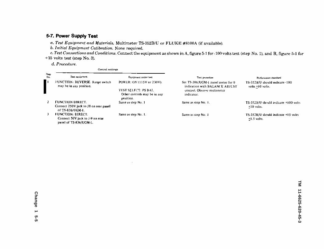
5-7
5-9
1-11-1
2-12-12-12-1
2-3
2-32-42-5
3-13-13-5
3-103-103-10
4-14-14-24-2
5-15-15-15-25-2
5-55-7
5-11
*This manual supersedes TM 11-6625-620-45-3, 6 December 1966.
*TM 11-6625-620-45-3
Paragraph Page
----------------------------------------------------
--------------------------------------
---------------------------------------------------
2-5 2-3
2-3
3-33-4 3-5
3-8
4-4
5-35-6
5-8
i

TM 11-6625-620-45-3
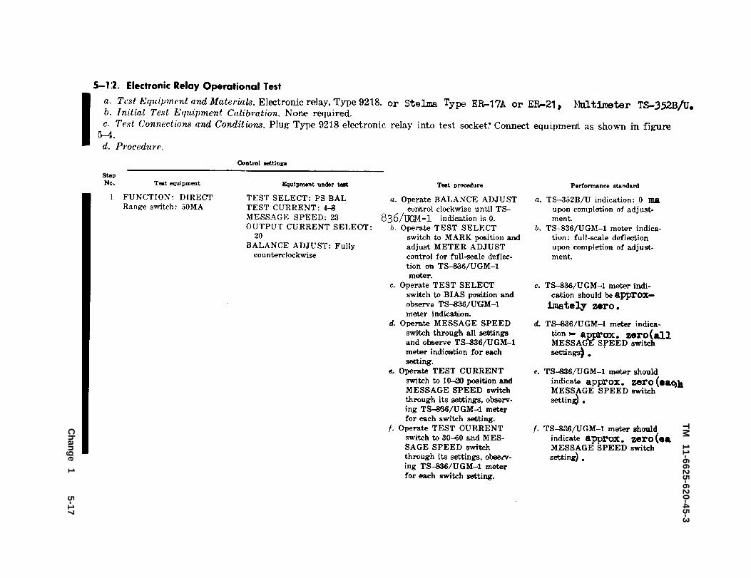
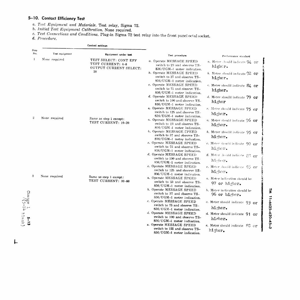
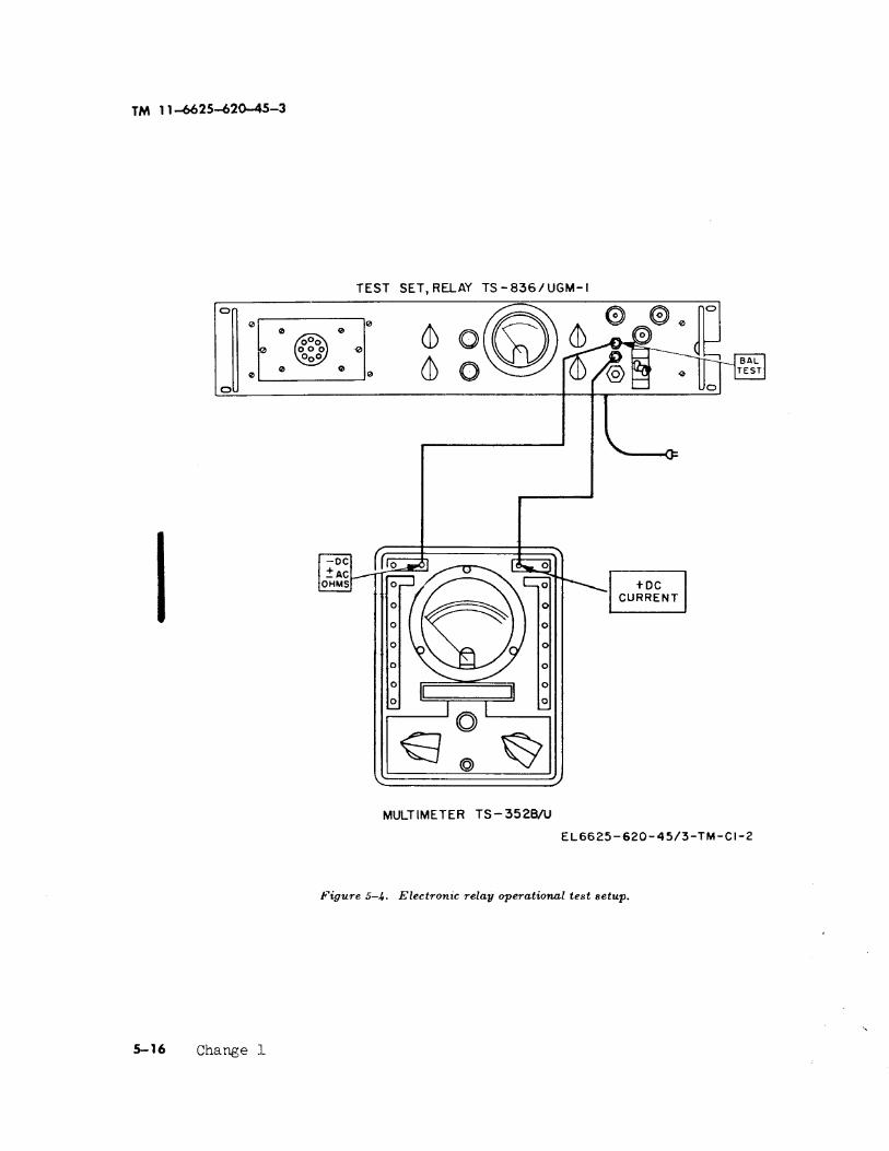
Contact efficiency test---------------------------------------------------------------------------- 5-10Contact bounce test------------------------------------------------------------------------------ 5-11Electromic relay operational test----------------------------------------------------------- 5-12Summary of performance standards------------------------------------------------------- 5-13
CHAPTER 6. DEPOT MAINTENANCE
General---------------------------------------------------------------------------------6-1Maintenance procedures - - - - - - - - - - - - - - - - - - - - - - - - - - - - - - - - - - - - - - - - - - - - - - - - - - 6 - 2
CHAPTER 7. DEPOT OVERHAUL STANDARDS
APPENDix
Applicability of depot overhaul standards--------------------------------------------------7-1Applicable references----------------------------------------------------------------------------------7-2Depot overhaul requirements --------------------------------------------------------------------7-3REFERENCES ----------------------------------------------------------------------------------------------
Page
5-136-156-16
6-16-1
7-17-17-1A-1
ii
Paragraph
1-1. Scope
TM 11-6625-620-45-3
CHAPTER 1INTRODUCTION
a. This manual contains general support anddepot maintenance instructions for Test Set,Relay TS-836/UGM-1. It includes instructionsappropriate to general support and depot mainte-nance for troubleshooting, testing, aligning, andrepairing the equipment. It also lists tools,materials, and test equipment required for gen-eral support and depot maintenance. Functionalanalysis of the equipment is covered in thischapter.
b. The complete technical manual for thisequipment includes TM 11-6625-620-12 and TM11-6625-620-25P-3.
1-2. Indexes of Publicationsa. Refer to the latest issue of DA Pam 310-4 to
determine whether there are new editions,changes, or additional publications pertaining tothe equipment.
b. Refer to DA Pam 310-7 to determine whetherthere are modification work orders (MWO's)pertaining to the equipment.
1-3. Forms and Recordsa. Reports of Maintenance and Unsatisfactory
Equipment. Maintenance forms, records, andreports which are to be used by maintenancepersonnel at all maintenance levels are listed in
and prescribed by TM 38-750.b. Report of Packaging and Handling Deficien-
ties. Fill out and forward DD Form 6 (Report ofPackaging and Handling Deficiencies) as pre-scribed in AR 700-58/NAVSUP PUB 378/AFR71-4/MCO P4030.29, and DSAR 4145.8.
c. Discrepancy in Shipment Report (DISREP)(SF 361). Fill out and forward Discrepancy inShipment Report (DISREP) (SF 361) as pre-scribed in AR 55-38/NAVSUPINST 4610.33/AFM75-.18/MCO P4610.19A, and DSAR 4500.15.
d. Report of errors, omissions, and recommen-dations for improving this manual by the indi-vidual user is encouraged. Reports should besubmitted on DA Form 2028 (RecommendedChanges to Publications and Blank Forms) andforwarded direct to Commanding General, USArmy Electronics Command, ATTN: AMSEL-MA-ML, Fort Monmouth, NJ 07703.
1-4. Destruction of Army MaterielDemolition and destruction of this equipment willbe under the direction of the commander and inaccordance with TM 750-422-2.
1-5. Administrative StorageFor procedures, forms and records, and inspec-tions required during administrative storage ofthis equipment, refer to TM 740-90-1.
Change 1 1-1


TM 11-6625-620-45-3
CHAPTER 2
FUNCTIONING OF EQUIPMENT
Section I. BLOCK PROGRAM
2-1. General(fig. 2-1)
The TS–836/UGM–1 checks the operatingcharacteristics of electronic and mechanical re-lays at different signal speeds. The TS-836/UGM-1 consists of three major sections:power supply circuits, timing circuits, and out-put circuits. The manner in which operatingand signal voltages are developed is illustratedin the block diagram and discussed. in the para-graphs below.
2-2. Power Supply
(fig. 2-1)The output voltages of the power supply are
+ 100, –100, and +15 volts direct current (dc).These voltages are developed from a 115– or220–volt alternating current (ac) power source.The input power is applied to the primary oftransformer T1 which develops 120–volts acacross each of the secondary windings. The120–volt ac is applied to a –100-volt rectifierand to a +100–volt rectifier. These rectifiersconvert the 120 volts ac to –100, + 100, and+ 15 volts dc. These dc voltages are main-tained at a constant level by their respectiveregulator circuits.
2-3. Timing Circuit(fig. 2-1)
The timing ciruit generates contant marksand spaces (reversals ), to simulate messages,which are applied to the relay under test. Thereversals are generated by a free-running mul-tivibrator Q1–Q2. The multivibrator producesa sawtooth output at selectable rates and ap-plies it to a bistable multivibrator Q3-Q4. Thebistable multivibrator reshapes the sawtoothsignal and changes the voltage levels to ap-proximately +15 and +0.4 volts. These vol-tages are applied to emitter follower Q5. Theoutput of the emitter follower is used to driveelectronic switch Q5 in the output circuit (Pam2–4) .
2-4. Output Circuit(fig. 2-1)
The output circuit couples the test voltagesto the relay under test and allows the outputof the relay to be coupled to EXTERNALOUTPUT jack J3 where it can be observed ona distortion meter or oscilloscope. The type ofrelay under test determines the current requiredto operate the relay coil. The current controlsection of the output circuit supplies the currentto the relay through the relay test socket.Electronic switch Q5 simulates message trans-mission for the relay under test by providingreversals in the form of circuit openings andclosings.
2-1

Figure 2-1.
TM
11-6625-620-45-3
2-2
TM 11-6625-620-45-3
Section II. DETAILED FUNCTIONING OF ELECTRONIC CIRCUITS
2-5. General(fig. 2-1)
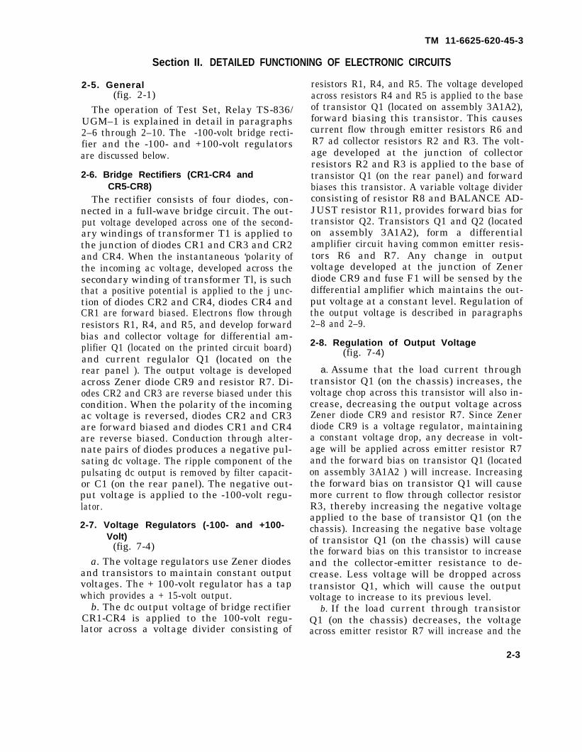
The operation of Test Set, Relay TS-836/UGM–1 is explained in detail in paragraphs2–6 through 2–10. The -100-volt bridge recti-fier and the -100- and +100-volt regulatorsare discussed below.
2-6. Bridge Rectifiers (CR1-CR4 andCR5-CR8)
The rectifier consists of four diodes, con-nected in a full-wave bridge circuit. The out-put voltage developed across one of the second-ary windings of transformer T1 is applied tothe junction of diodes CR1 and CR3 and CR2and CR4. When the instantaneous ‘polarity ofthe incoming ac voltage, developed across thesecondary winding of transformer Tl, is suchthat a positive potential is applied to the j unc-tion of diodes CR2 and CR4, diodes CR4 andCR1 are forward biased. Electrons flow throughresistors R1, R4, and R5, and develop forwardbias and collector voltage for differential am-plifier Q1 (located on the printed circuit board)and current regulalor Q1 (located on therear panel ). The output voltage is developedacross Zener diode CR9 and resistor R7. Di-odes CR2 and CR3 are reverse biased under thiscondition. When the polarity of the incomingac voltage is reversed, diodes CR2 and CR3are forward biased and diodes CR1 and CR4are reverse biased. Conduction through alter-nate pairs of diodes produces a negative pul-sating dc voltage. The ripple component of thepulsating dc output is removed by filter capacit-or C1 (on the rear panel). The negative out-put voltage is applied to the -100-volt regu-lator.
2-7. Voltage Regulators (-100- and +100-Volt)
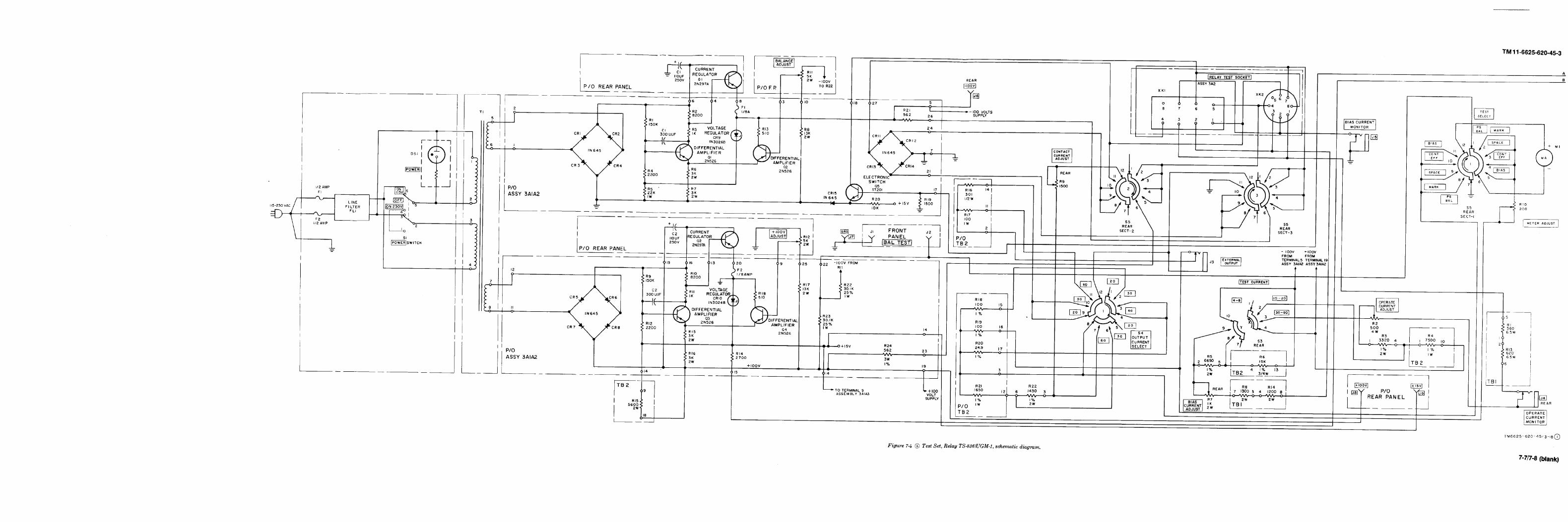
(fig. 7-4)a. The voltage regulators use Zener diodes
and transistors to maintain constant outputvoltages. The + 100-volt regulator has a tapwhich provides a + 15-volt output.
b. The dc output voltage of bridge rectifierCR1-CR4 is applied to the 100-volt regu-lator across a voltage divider consisting of
resistors R1, R4, and R5. The voltage developedacross resistors R4 and R5 is applied to the baseof transistor Q1 (located on assembly 3A1A2),forward biasing this transistor. This causescurrent flow through emitter resistors R6 andR7 ad collector resistors R2 and R3. The volt-age developed at the junction of collectorresistors R2 and R3 is applied to the base oftransistor Q1 (on the rear panel) and forwardbiases this transistor. A variable voltage dividerconsisting of resistor R8 and BALANCE AD-JUST resistor R11, provides forward bias fortransistor Q2. Transistors Q1 and Q2 (locatedon assembly 3A1A2), form a differentialamplifier circuit having common emitter resis-tors R6 and R7. Any change in outputvoltage developed at the junction of Zenerdiode CR9 and fuse F1 will be sensed by thedifferential amplifier which maintains the out-put voltage at a constant level. Regulation ofthe output voltage is described in paragraphs2–8 and 2–9.
2-8. Regulation of Output Voltage(fig. 7-4)
a. Assume that the load current throughtransistor Q1 (on the chassis) increases, thevoltage chop across this transistor will also in-crease, decreasing the output voltage acrossZener diode CR9 and resistor R7. Since Zenerdiode CR9 is a voltage regulator, maintaininga constant voltage drop, any decrease in volt-age will be applied across emitter resistor R7and the forward bias on transistor Q1 (locatedon assembly 3A1A2 ) will increase. Increasingthe forward bias on transistor Q1 will causemore current to flow through collector resistorR3, thereby increasing the negative voltageapplied to the base of transistor Q1 (on thechassis). Increasing the negative base voltageof transistor Q1 (on the chassis) will causethe forward bias on this transistor to increaseand the collector-emitter resistance to de-crease. Less voltage will be dropped acrosstransistor Q1, which will cause the outputvoltage to increase to its previous level.
b. If the load current through transistorQ1 (on the chassis) decreases, the voltageacross emitter resistor R7 will increase and the
2-3
TM 11-6625-620-45-3
flow of current through transistor Q1 (locatedon assembly 3A1A2 ) will decrease. A decreasein conduction of transistor Q1 will cause theforward bias on transistor Q1 (on the chassis)to decrease and the collector-to-emitter resis-tance to increase. More voltage will be droppedacross transistor Q1, which wiil cause the out-put voltage to decrease to a normal level. c. The differential amplifier senses very
small as well as very large load changes. Zenerdiode CR9 provides a fixed reference voltagefor the emitter of transistor Q1 (on the chassis)This action allows maximum variation acrosschassis transistor Q1 to obtain the best possibleregulation.
(1)
(2)
+100-volt regulutor outputs. The+100-volt regulator provides + 100volts in the same manner as the –l00-volt regulator provides -100 voltsAlso, the input voltage divider, in the+100-volt regulator circuit, consistingof resistors R9, R12, and R15 (lo-cated on terminal board TB2 ), de-velops +15 volts operating power forthe timing circuit. Capacitors Cl andC2 (on the chassis) are used for fil-tering. Variable resistors R11 and R12adjust the output of the –100- and+100-volt regulators, respectively.
Balancing regulator outputs. ResistorsR22 and R23 form a voltage divideracross the output of both regulators.When the voltage at the junction ofmisters R22 and R23 is not zero acomparison is made of the differencein output voltages of the regulators.This difference can be measured withvoltmeter connected to BAL TESTjacks J1 and J2 on the front panelor by connecting PERCENT meterMl into the circuit (junction of re-sistors R22 and R23 ) by placing theTEST SELECT switch (on the frontpanel) in the PS BAL position.
2-9. Current Determining Circuit(fig. 7-4)
a. The regulated outputs of the -100- and+100-volt regulators are applied through relaysocket XK1 or XK2 to the coils of the relayunder test to determine contact efficiency
2-4
and bias distortion. Bias current is developedfrom the -100-volt line through resistors R5,R6, R7 (BIAS CURRENT ADJUST), R8 andR14, together with section Y of TEST CUR-RENT switch S3 (forming a current-limitingnetwork). TEST CURRENT switch S3 selectsone of three bias current levels (4, 10, or 30milliamperes (ma) ) for the bias coil of therelay under test by short circuiting either re-sistor R6 on terminal board TB2 or resistorsR5 and R6. Resistor R7 (BIAS CURRENTADJUST) adjusts the bias current applied tothe bias coil of the relay under test. The biascurrent can be monitored at BIAS CURRENTMONITOR jack J5 on the rear panel.
b. Operating current is developed from the+100-volt line through resistors R1, R13 (onterminal board TB1), Rs (OPERATE CUR-RENT ADJUST), R3, and R4, together withSECTION X of TEST CURRENT switch S3(forming a current-limiting network). TESTCURRENT switch S3 selects one of three op-erate current levels (8, 20 or 60 ma) for theoperate coil of the relay under test by shortcircuiting either resistor R4 (on terminal boardTB2) or resistors R3 and R4. Resistor R2(OPERATE CURRENT ADJUST) adjustthe operate current applied to the operate coilof the relay under test. The operate currentcan be monitored at OPERATE CURRENTMONITOR jack J4 on the rear panel.
c. When the TEST SELECT switch is in anyposition except PS BAL, contact current forthe relay is supplied by the -100- and +100-volt lines. These voltages, connected throughresistors R21 and R24, are present at terminals4 and 7 of relay socket XK2. When the biasand operating currents are wed through therespective relay coil, a polarized signal is pro-duced at terminal 6 of relay socket XK2. Thissignal is retified by a bridge rectifier con-sisting of diodes CR11 through CR14, and thenapplied through OUTPUT CURRENT SELECTswitch S4 to current-limiting resistors R16through R22 to PERCENT meter M1 where anindication of current flowing through the re-lay contacts can be observed. An oscilloscopeor distortion meter can be connected to EX-TERNAL OUTPUT jack J3 to measure dis-tortion.
TM 11-6625-620-45-3
2-10. Timing Circuit(fig. 7-4)
The timing circuit consists of a free-runningmultivibrator (Q1–Q2), a bistable (Q3–Q4),emitter follower (A3Q5), and an electronicswitch (A2Q5). The timing circuit, by circuitopenings and closings, simulates message con-ditions. The timing circuit, with the exceptionof the electronic switch, is located on assembly3A1A3. The electronic switch is located onassembly 3A1A2.
a. Multivibrator Q1–Q2. The multivibratorcircuit is a stardard free-running multivibrator,connected to MESSAGE SPEED switch S2through frequency determining capacitors C3through C12. These capacitors are individuallyswitched into or out of the circuit by MES-SAGE SPEED switch S2, depending on thefrequency to be selected. The capacitors thatare switched into the circuit operate in conjunc-tion with base resistors R3, R4, and R5 to de-termine the frequency of the rnultivibratm.Resistor R1 and capacitors C1 and C2 form adecoupling network. Resistors R2 and R7 arecollector load resistors. Resistor R6 is a com-mon emitter bias resistor for the multivibrator.The output of the multivibrator, developed atthe collector of transistor Q2, is coupled throughcapacitor C16 to a steering diode (CR1 or CR2)and applied to bistable Q3–Q4.
b. Bistable Multivibrator Q3–Q4. The bi-stable multivibrator circuit consists of a single,standard, bistable multivibrator with a singleinput. The input signal, obtained from multi-vibrator Q1–Q2, is applied through steeringdiode CR1 or CR2. With transistor Q4 con-
ducting, the higher of the two positive basevoltages appears at the anode of diode CR2. Anegative transition from the multivibrator,applied to the junction of diodes CR1 and CR2,forward biases diode CR2, thereby applyingthe negative pulse to the base of transistorQ4, which turns off transistor Q4 and turnson transistor Q3. The next negative transition,applied to the junction of diodes CR1 and CR2,forward biases diode CR1, thereby applyingthe negative pulse to the base of transistorQ3 which turns off transistor Q3 and turns ontransistor Q4. Capacitors C13 and C14 togetherwith resistors R14 and R16 determine switch-ing time for bistable Q3–Q4. Resistors R12and R15 provide coupling between transistorsQ3 and Q4. Resistors R11 and R17 are collectorload resistors. Resistor R13 and capacitor C15are emitter components common to transistorsQ3 and Q4. The output of the bistable multi-vibrator, developed at the collector of transis-tor Q4, is applied to the input of emitter fol-lower Q5.
c. Emitter Follower Q5 and ElectronicSwitch Q5. Emitter follower Q5 isolates elec-tronic switch Q5. The output of bistable Q3–Q4 (b above) is applied to the base of tran-sistor Q5. When transistor Q4 is conducting,the output voltage is not high enough for tran-sistor Q5 to conduct. However, when transistorQ4 is not conducting, the positive collectorvoltage causes transistor Q5 to conduct. Cur-rent flows through emitter resistors R18 andR19. The voltage drop across resistor R19 turnson transistor Q5. Current flows throughQ5 and diode CR15 to operate the coil of therelay under test.
2-5


TM 11-6625-620-45-3
CHAPTER 3
TROUBLESHOOTING
Section I. GENERAL TROUBLESHOOTING TECHNIQUES
Warning: Use care in troubleshooting ormaking repairs in this equipment. Voltages ashigh as 230 volts ac are present in the powersupply. Use insulated test probes when makingthe required voltage measurements. Alwaysdisconnect power from the equipment beforetouching any internal part.
3-1. General Instructions
Troubleshooting at the general support anddepot maintenance categories includes all thetechniques outlined for organizational sup-port maintenance and any special or additionaltechniques required to isolate a defective part.Section H describes localizing and isolatingtechniques to be used by general support anddepot maintenance personnel. Observe the fol-lowing precautions while troubleshooting theTS-836/UGM-1:
a. This equipment contains transistor cir-cuts; therefare, never connect test equipment(other than multimeter and vtvm’s) outputsdirectly to a transistor circuit; use a couplingcapacitor.
b. Before using any ohmmeter to test tran-sistors or transistor circuits, check the open-circuit voltage across the ohmmeter test leads.Do not use the ohmmeter if the open-circuitvoltage exceeds 1.5 volts. Do not use the RX1resistance range of the ohmmeter since the RX1range normally connects the ohmmeter in-ternal battery directly across the test leads andthe comparatively high current (50 ma or more)may damage the transistor under test.
c. Make test equipment connections withcare so the shorts will not be caused by exposedtest equipment connectors. Tape or use sleeving(spaghetti) on test prods or clips to leave as
little exposed metal as needed to make contactto the circuit under test.
d. The equipment internal power supply isrecommened as the source of power when serv-icing this transistorized equipment. However,when external power sources are used, observepolarity. Polarity reversal may damage thetransists or electro!ytic capacitor in the circuit. If an external source is used in place of theinternal source, it must have good voltageregulation and low ac ripple. Good regulationis important because the output voltage of apower supply that. has poor regulation mayexceed the maximum voltage rating of the tran-sistors in the equipment being tested.
3-2. Organization of TroubleshootingProcedures
a. General. The first step in servicing adefective unit equipment is to sectionalize thefault. Sectionalization means tracing the faultto the major equipment component. The sec-ond step is to localize the fault. Localizationmeans tracing the fault to the defective stageor unit responsible for the abnormal condition.The third step is isolation. Isolation meanstracing the fault to the defective part; figures3–1 through 3–6 are parts location diagrams.Some faults, such as burned-out resistors, arc-ing or shorted transformers, can often be iso-lated by sight, smell, or hearing. The majorityof faults, however, must be isolated by checkingvoltages, resistance, and signal levels.
b. Sectionalization. Following are a groupof tests arranged to reduce unnecessary work,and to aid in tracing trouble in a defectiverelay test set. A relay test set consists of threemajor sections: the power supply circuits, thetiming circuits, and the output circuits. The
3-1
TM 11-6625-620-45-3
first step is to locate the section or sections atfault by
(1)
(2)
using the following methods:Visual inspection. The purpose of avisual inspection is to locate the faultswithout testing or measuring cir-cuits. All moving parts, switch andcontrol settings, or other visual signsshould be observed and an attemptmade to sectionalize the fault to aparticular section.Operational tests. Operational testsfrequently indicate the general loca-tion of trouble. In many instances, thetests will help in determining theexact nature of the fault. Operatinginstructions given in paragraph 3-7,TM 11–6625–620–12 provide a goodoperational check.
c. Localization. The tests listed in e belowand in paragraph 3-5 will aid in localizing thetrouble within that stage by voltage, resistance,or continuity measurements. Use the trouble-shooting chart to localize trouble to a particularstage or part.
d. Isolation. Procedures for isolating trou-bles are given in paragraph 3–6. These pro-cedures are to be performed at general supportand depot maintenance categories.
e. Techniques. In performing the sectionali-zation, localization, and isolation procedures,one or more of the techniques below may beused. Use these techniques only as indicatedand observe all cautions.
(1) Voltage measurements. This equip-ment is transistorized; therefore ob-serve all cautions given in paragraph3–1 to prevent transistor damage.Make voltage and resistance measure-ments in this equipment only asspecified. When measuring voltages,use tape or sleeving to insulate theentire test prod, except for the ex-treme tip. A momentary short circuitcan ruin a transistor. Use resistor andcapacitor color codes (fig. 7–1 and7–2) to determine values of color-coded components. Compare voltageand resistance data obtained fromreadings taken on assembly 3A1A2,assembly 3A1A3, and chassis 3A1 with
(2)
(3)
(4)
(5)
voltage and resistance data for normalreadings (fig. 3–7, 3-8, and 7-3, re-spectively).
Resistance measurements. Performresistance measurements in this equip-ment only as directed on voltage andresistance charts or diagrams. Useonly the ohmmeter ranges specfied(para 3-1), otherwise indications ob-tained will not be valid. Also, thepolarity of the ohmmeter connectionsmust be strichtly observed, where indicated.
Caution: Before using any ohm-meter to test transistors or transistor
circuits, refer to the precautions givenin paragraph 3-1.
Test points. This euipment is equip-ped with test jacks to circuits. The testpoints should be used wheneverpossible to avoid needless disassem-bly of the equipment. These testpaints are shown on the schematicdiagram (fig. 7-4) and on the partslocation diagrams (fig. 3-1 through3-6).Intermittent troubles. In all the test,the possibility of intermittent troublesshould not be overlooked. If present,this type of trouble can often be madeto appear by tapping or jarring theequipment. Make a visual inspectionof the wiring and connections to theunits of the set. Minute cracks inprinted circuit boards can cause inter-mittent operation. A magnifying glassis helpful in locating defects in printedcircuit boards. Continuity measure-ments of printed circuit conductorsmay be made using the same techniqueordinarily used on hidden conven-tional wiring; observe the ohmmeterprecautions ((2) above).Resistor and capacitor color codediagrams. Color code diagrams forresistars and capacitors (fig. 7-1 and7–2) provide pertinent resistance capactance, voltage rating, and toler-ance information.
3-2

Figure 3-1.
TM
11-6625-620-45-33-3
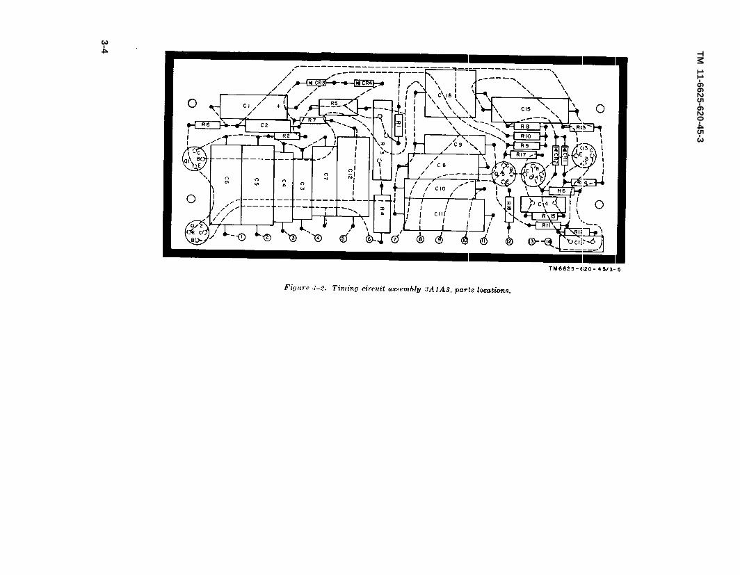
Figure 3-2.
TM
11-6625-620-45-3
3-4
TM 11-6625-620-45-3
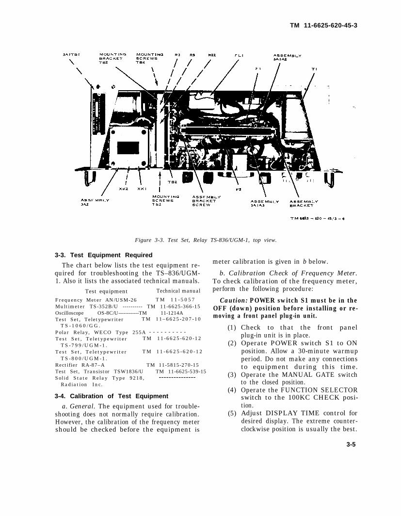
Figure 3-3. Test Set, Relay TS-836/UGM-1, top view.
3-3. Test Equipment Required
The chart below lists the test equipment re- meter calibration is given in b below.
quired for troubleshooting the TS–836/UGM- b. Calibration Check of Frequency Meter.1. Also it lists the associated technical manuals. To check calibration of the frequency meter,
Test equipment Technical manual perform the following procedure:
Frequency Meter AN/USM-26 T M 1 1 - 5 0 5 7 Caution: POWER switch S1 must be in theMultimeter TS-352B/U ---------- TM 11-6625-366-15 OFF (down) position before installing or re-Oscilloscope OS-8C/U------------TM 11-1214ATest Set, Teletypewriter TM 11–6625-207-10 moving a front panel plug-in unit.
T S - 1 0 6 0 / G G .Polar Relay, WECO Type 255A
(1)- - - - - - - - - -
Test Set, Teletypewriter TM 11-6625-620-12T S - 7 9 9 / U G M - 1 . (2)
Test Set, Teletypewriter T M 1 1 - 6 6 2 5 - 6 2 0 - 1 2T S - 8 0 0 / U G M - 1 .
Rectifier RA-87–A TM 11-5815-270-15Test Set, Transistor TSW1836/U TM 11-6625-539-15Solid State Relay Type 9218, (3)---------------
Radiation Inc.
3-4. Calibration of Test Equipment(4)
a. General. The equipment used for trouble-shooting does not normally require calibration. (5)However, the calibration of the frequency metershould be checked before the equipment is
Check to that the front panelplug-in unit is in place.Operate POWER switch S1 to ONposition. Allow a 30-minute warmupperiod. Do not make any connectionsto equipment during this time.Operate the MANUAL GATE switchto the closed position.Operate the FUNCTION SELECTORswitch to the 100KC CHECK posi-tion.Adjust DISPLAY TIME control fordesired display. The extreme counter-clockwise position is usually the best.
3-5
TM 11-6625-620-45-3
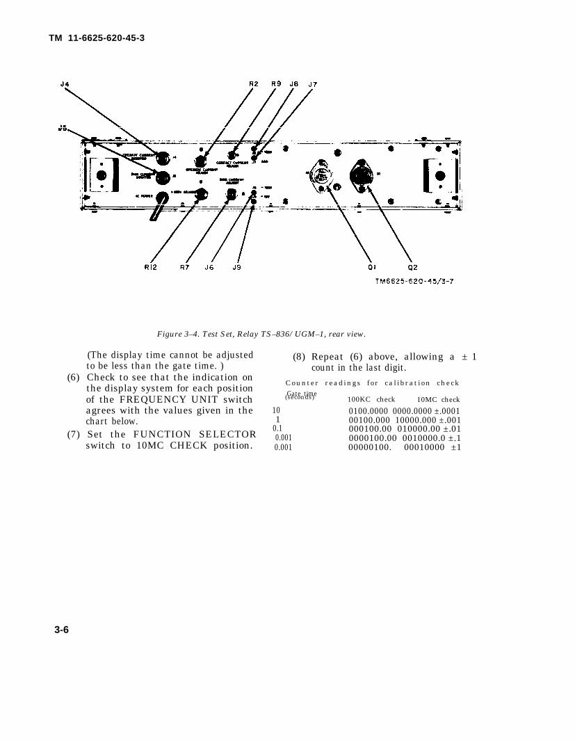
Figure 3–4. Test Set, Relay TS–836/UGM–1, rear view.
(The display time cannot be adjustedto be less than the gate time. )
(6) Check to see that the indication onthe display system for each positionof the FREQUENCY UNIT switch
(8) Repeat (6) above, allowing a ± 1count in the last digit.
Counter readings for ca l ibrat ion checkGate time
100KC check 10MC check
agrees with the values given in thechart below.
(7) Set the FUNCTION SELECTORswitch to 10MC CHECK position.
(seconds)
0100.0000 0000.0000 ±.000100100.000 10000.000 ±.001
101
0.10.0010.001
000100.00 010000.00 ±.010000100.00 0010000.0 ±.100000100. 00010000 ±1
3-6
TM 11-6625-620-45-3
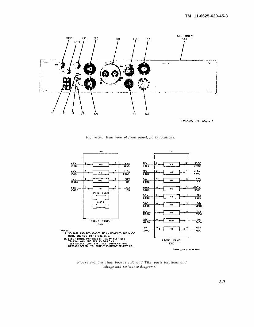
Figure 3-5. Rear view of front panel, parts locations.
Figure 3–6. Terminal boards TB1 and TB2, parts locations andvoltage and resistance diagrams.
3-7
TM 11-6625-620-45-3
Section II. TROUBLESHOOTING TS-836/UGM-1
3-5. Localizing Troubles
a. General. The troubleshooting chart (cbelow) outlines procedures for localizingtroubles to an individual circuit or component.Follow the procedures given in the trouble-shooting chart whenever improper results areobtained after performing the maintenacechecks (TM 11–6625–620–12). Depending onthe nature of the operational symptoms, oneor more of the localizing procedures will benecessary to locate the fault. Once the troubleis localized to a particular stage or circuit, usevoltage and resistance measurements (para 3-6) to isolate the trouble to a particular de-fective part.
b. Use of Chart. The troubleshooting chartlists indications that the repairman observeswhile performing the maintenance checks andspecifies the probable trouble and procedurerequired. Also, the probable trouble column inthe chart localizes the trouble to am individualassembly or curcuit on the assembly. The physi-cal location of each assembly is indicated asfollows: 3A1 for components mounted onthe chassis assembly, 3A2 for componentsmounted on the test socket assembly, 3A3 forcapacitor mounting assembly, and 3A4 fortransformer mounting assembly. In the chart,reference is made as required to figures 3–1through 3-6.
c. Troubleshooting Chart.
Note. Perform the procedures in the operator’s daily preventive maintenance checks and services chart(TM 11-6605-620-12) before using this chart, unless trouble has already been localized.
1.
2.
3.
4.
5.
3-8
Indication
Power indicator lamp DS1does not light.
Fuse F1 or F2 opens, repeat-edly, when POWER switchis operated to ON position.
Unable to balance powerSupply.
Unable to obtain fullscaledeflection using METERADJ control,
No meter indication for allTEST SELECT switch
Probable trouble
a. Defective fuseholder XF1 orXF2.
b. Filter FL1. ---------------------------
Defective power supply circuit onassembly 3A1A2.
a. Defective resistor R22 or R23on assembly 3A1A2.
b. Defective –100 volts regulatorQ1-Q2 on assembly 3A1A2.
c. Defective -100 volts rectifierCR1-CR4 on assembly3A1A2.
d. Defective series regulator Q1on rear panel.
a. Defective METER ADJ var-iable resistor 3A1R10 on
front panel.b. Defective meter 3A1Ml on
front panel.a. Defective meter 3A1M1 on
front panel.positions except PS BAL. b. Defective Test TEST SELECT
switch 3A1S5 on frontpanel.
Procedure
a. Check fuseholders. Replace ifdefective (fig. 3-5).
b. Check filter for continuity.Replace if defective (fig.3–3).
a. Check power supply circuitfor shorts. Replace defectivecomponent (fig. 3-1).
a. Check resistors. Replace de-fective component (fig. 3-1).
b. Check Q1-Q2 circuit by per-forming voltage measure-ments (para 3-7). Replacedefective component (fig.3-1) .
c. Check rectifiers. Replace de-fective component (fig. 3-1).
d. Perform voltage and resistancemeasurements (para 3-7).Replace if defective (fig.3-4).
a. Check resistor. Replace ifdefective (fig. 3-4).
b. Check meter. Replace if de-fective (fig. 3-5).
a. Check meter. Replace if de-fective (fig. 3–5).
b. Check switch. Replace if de-fective (fig. 3-5).
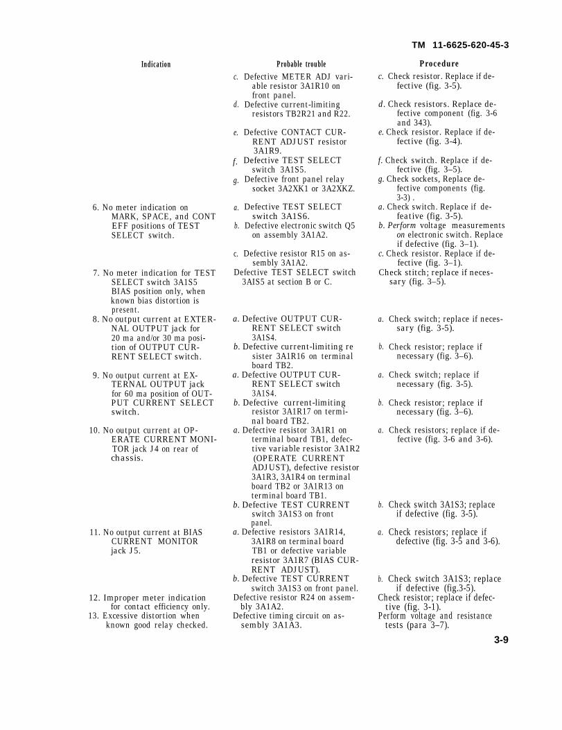
Indication
6. No meter indication onMARK, SPACE, and CONTEFF positions of TESTSELECT switch.
7. No meter indication for TESTSELECT switch 3A1S5BIAS position only, whenknown bias distortion ispresent.
8. No output current at EXTER-NAL OUTPUT jack for20 ma and/or 30 ma posi-tion of OUTPUT CUR-RENT SELECT switch.
9. No output current at EX-TERNAL OUTPUT jackfor 60 ma position of OUT-PUT CURRENT SELECTswitch.
10. No output current at OP-ERATE CURRENT MONI-TOR jack J4 on rear ofchassis.
11. No output current at BIASCURRENT MONITORjack J5.
12. Improper meter indicationfor contact efficiency only.
13. Excessive distortion whenknown good relay checked.
c.
d.
e.
f.
g.
a.
b.
c.
Probable troubleDefective METER ADJ vari-
able resistor 3A1R10 onfront panel.
Defective current-limitingresistors TB2R21 and R22.
Defective CONTACT CUR-RENT ADJUST resistor3A1R9.
Defective TEST SELECTswitch 3A1S5.
Defective front panel relaysocket 3A2XK1 or 3A2XKZ.
Defective TEST SELECTswitch 3A1S6.
Defective electronic switch Q5on assembly 3A1A2.
Defective resistor R15 on as-sembly 3A1A2.
Defective TEST SELECT switch3AIS5 at section B or C.
a. Defective OUTPUT CUR-RENT SELECT switch3A1S4.
b. Defective current-limiting resister 3A1R16 on terminalboard TB2.
a. Defective OUTPUT CUR-RENT SELECT switch3A1S4.
b. Defective current-limitingresistor 3A1R17 on termi-nal board TB2.
a. Defective resistor 3A1R1 onterminal board TB1, defec-tive variable resistor 3A1R2(OPERATE CURRENTADJUST), defective resistor3A1R3, 3A1R4 on terminalboard TB2 or 3A1R13 onterminal board TB1.
b. Defective TEST CURRENTswitch 3A1S3 on frontpanel.
a. Defective resistors 3A1R14,3A1R8 on terminal boardTB1 or defective variableresistor 3A1R7 (BIAS CUR-RENT ADJUST).
b. Defective TEST CURRENTswitch 3A1S3 on front panel.
Defective resistor R24 on assem-bly 3A1A2.
Defective timing circuit on as-sembly 3A1A3.
TM 11-6625-620-45-3
Procedurec. Check resistor. Replace if de-
fective (fig. 3-5).
d. Check resistors. Replace de-fective component (fig. 3-6and 343).
e. Check resistor. Replace if de-fective (fig. 3-4).
f. Check switch. Replace if de-fective (fig. 3–5).
g. Check sockets, Replace de-fective components (fig.3-3) .
a. Check switch. Replace if de-feative (fig. 3-5).
b. Perform voltage measurementson electronic switch. Replaceif defective (fig. 3–1).
c. Check resistor. Replace if de-fective (fig. 3–1).
Check stitch; replace if neces-
a.
b.
a.
b.
a.
b.
a.
b.
sary (fig. 3–5).
Check switch; replace if neces-sary (fig. 3-5).
Check resistor; replace ifnecessary (fig. 3–6).
Check switch; replace ifnecessary (fig. 3-5).
Check resistor; replace ifnecessary (fig. 3–6).
Check resistors; replace if de-fective (fig. 3-6 and 3-6).
Check switch 3A1S3; replaceif defective (fig. 3-5).
Check resistors; replace ifdefective (fig. 3-5 and 3-6).
Check switch 3A1S3; replaceif defective (fig.3-5).
Check resistor; replace if defec-tive (fig. 3-1).
Perform voltage and resistancetests (para 3–7).
3-9
TM 11-6625-620-45-3
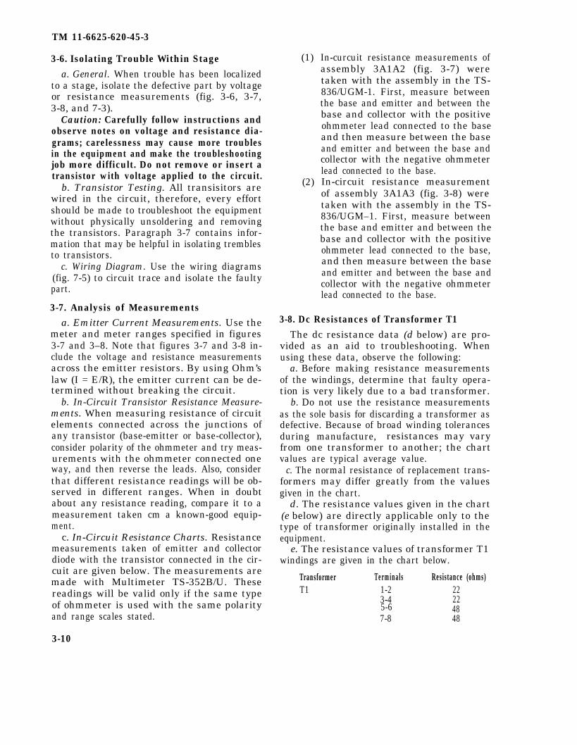
3-6. Isolating Trouble Within Stagea. General. When trouble has been localized
to a stage, isolate the defective part by voltageor resistance measurements (fig. 3-6, 3-7,3-8, and 7-3).
Caution: Carefully follow instructions andobserve notes on voltage and resistance dia-grams; carelessness may cause more troublesin the equipment and make the troubleshootingjob more difficult. Do not remove or insert atransistor with voltage applied to the circuit.
b. Transistor Testing. All transisitors arewired in the circuit, therefore, every effortshould be made to troubleshoot the equipmentwithout physically unsoldering and removingthe transistors. Paragraph 3-7 contains infor-mation that may be helpful in isolating tremblesto transistors.
c. Wiring Diagram. Use the wiring diagrams(fig. 7-5) to circuit trace and isolate the faultypart.
3-7. Analysis of Measurementsa. Emitter Current Measurements. Use the
meter and meter ranges specified in figures3-7 and 3–8. Note that figures 3-7 and 3-8 in-clude the voltage and resistance measurementsacross the emitter resistors. By using Ohm’slaw (I = E/R), the emitter current can be de-termined without breaking the circuit.
b. In-Circuit Transistor Resistance Measure-ments. When measuring resistance of circuitelements connected across the junctions ofany transistor (base-emitter or base-collector),consider polarity of the ohmmeter and try meas-urements with the ohmmeter connected oneway, and then reverse the leads. Also, considerthat different resistance readings will be ob-served in different ranges. When in doubtabout any resistance reading, compare it to ameasurement taken cm a known-good equip-ment.
c. In-Circuit Resistance Charts. Resistancemeasurements taken of emitter and collectordiode with the transistor connected in the cir-cuit are given below. The measurements aremade with Multimeter TS-352B/U. Thesereadings will be valid only if the same typeof ohmmeter is used with the same polarityand range scales stated.
3-10
(1)
(2)
In-curcuit resistance measurements ofassembly 3A1A2 (fig. 3-7) weretaken with the assembly in the TS-836/UGM-1. First, measure betweenthe base and emitter and between thebase and collector with the positiveohmmeter lead connected to the baseand then measure between the baseand emitter and between the base andcollector with the negative ohmmeterlead connected to the base.In-circuit resistance measurementof assembly 3A1A3 (fig. 3-8) weretaken with the assembly in the TS-836/UGM–1. First, measure betweenthe base and emitter and between thebase and collector with the positiveohmmeter lead connected to the base,and then measure between the baseand emitter and between the base andcollector with the negative ohmmeterlead connected to the base.
3-8. Dc Resistances of Transformer T1The dc resistance data (d below) are pro-
vided as an aid to troubleshooting. Whenusing these data, observe the following:
a. Before making resistance measurementsof the windings, determine that faulty opera-tion is very likely due to a bad transformer.
b. Do not use the resistance measurementsas the sole basis for discarding a transformer asdefective. Because of broad winding tolerancesduring manufacture, resistances may varyfrom one transformer to another; the chartvalues are typical average value.
c. The normal resistance of replacement trans-formers may differ greatly from the valuesgiven in the chart.
d. The resistance values given in the chart(e below) are directly applicable only to thetype of transformer originally installed in theequipment.
e. The resistance values of transformer T1windings are given in the chart below.
Transformer Terminals Resistance (ohms)T1 1-2 22
3-4 2248
7-8 485-6
TM 11-6625-620-45-3
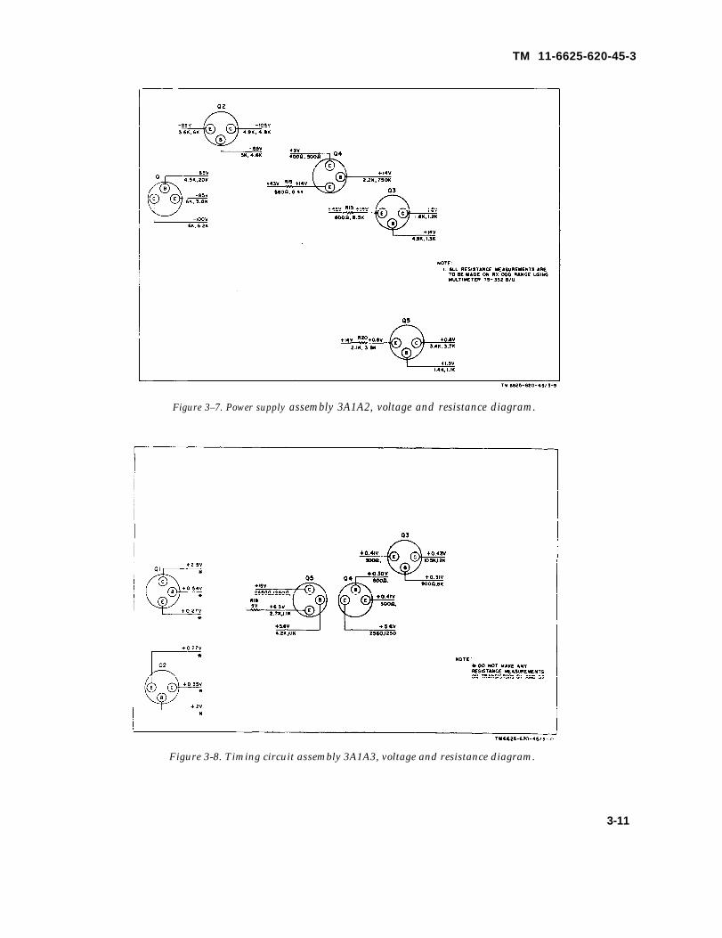
Figure 3–7. Power supply assembly 3A1A2, voltage and resistance diagram.
Figure 3-8. Timing circuit assembly 3A1A3, voltage and resistance diagram.
3-11

TM 11-6625-620-45-3
CHAPTER 4
GENERAL SUPPORT REPAIRS AND ALIGNMENT
4-1. General Parts ReplacementTechniques
Most of the parts in the TS–836/UGM–1can be reached easily and replaced withoutspecial procedures. However, the followingprecautions apply:
a. In the oscillator circuits, be sure that thelead length and position of the replacementpart is the same as the defective part to avoidcoupling and spurious oscillations.
b. Do not disturb the setting of controlswhen replacing parts unless the unit is to berealigned.
c. Use a pencil-type soldering iron with a25-watt maximum capacity and an isolatingtransformer between the soldering iron and theac line. Do not use a soldering gun since damag-ing Voltages can be induced in components.
d. When soldering transistor leads, solderquickly; wherever wiring permits, use a heatsink (such as a long-nosed pliers) betweenthe soldered joint and the transistor. Use ap-proximately the same length and dress oftransistor leads as used originally.
4-2. Disassembly of TS-836/UGM-1
Remove the unit from its carrying case (ifrequired ) by following the procedures givenin TM 11–6625–620–12.
a. Removal of Terminal Board TB1. Ter-minal board TB1 is mounted on the left sideof the TS–836/UGM–l. Remove terminalboard TB1 by performing the following pro-cedure:
(1)
(2)(3)
Remove the twoassembly 3A2 toRemove assemblyRemove the twoTB1.
screws that securethe front panel.3A2.screws that secure
(4) Remove TB1.b. Removal of Terminal Board TB2. Ter-
minal board TB2 is mounted on a bracket whichmust be removed to provide access to the ter-minal board. Remove terminal board TB2mounting bracket from the TS–836/UGM–1chassisdure:
(1)
(2)
by performing the following proce-
Remove the eight screws (8–32 pan-head) that hold terminal board TB2mounting bracket to the chassis; threescrews are located on the front panel,two screws are located on the rear ofthe chassis, and the remaining threescrews are located on the bottom ofthe chassis.Remove terminal board TB2 bracketby pulling straight out. Be carefulnot to break cable connections orsurrounding wires.
c. Removal of Assemblies 3A1A2 and8A1A3. Assemblies 3A1A2 and 3A1A3 aremounted on a bracket which must be removedto reach the rear of either assembly. Removeassemblies 3A1A2 and 3A1A3 as follows:
(1)
(2)
Remove the assembly bracket by re-moving the two screws (8–32 pan-head) on the bottom of the chassisand pulling the assemblies straightout.Remove assembly 3A1A2 cm 3A1A3from the assembly bracket by re-moving the four (8–32 panhead)screws. (Two screws are located ateach end of each assembly.)
d. Removal of Chassis-Mounted Components.When removing chassis-mounted components,first tag all connecting wires and then removethe mounting nuts.
4-1
TM 11-6625-620-45-3
4-3 Replacement Procedures
a. Replacement of Terminal Board TB1.Replace terminal board TB1 by reversing theprocedure given in paragraph 4–2a.
b. Replacement of Terminal Board TB2.Replace terminal board TB2 by reversing theprocedure given in paragraph 4–2b.
c. Replacement of Assemblies 3A1A2 and3A1A3. Replace assemblies 3A1A2 and 3A1A3by reversing the procedure given in paragraph4-2c.
d. Replacement of Chassis-Mounted Com-ponents. Replace chassis-mounted componentsby reversing the procedure given in paragraph4–2d.
4-4. Adjustments
The procedures for performing the +100-volt dc adjustment, the power supply balanceadjustment, the bias current adjustment, andthe operate current adjustment are given inchapter 5, TM 11–6625–620–12.
4-2
TM 11-6625-620-45-3
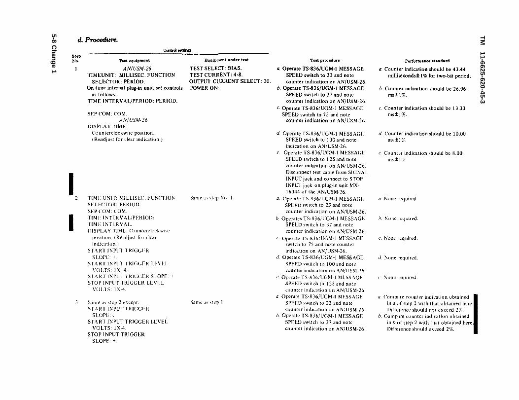
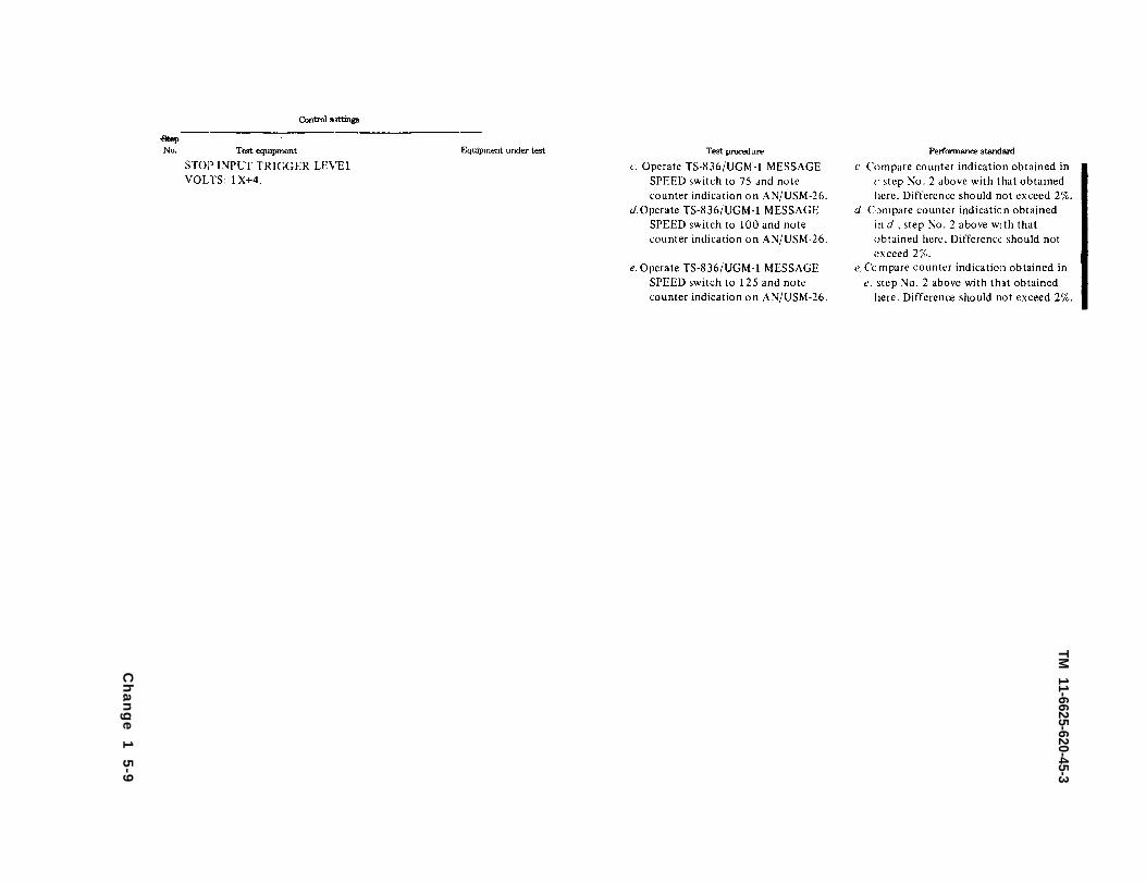
CHAPTER 5
GENERAL SUPPORT TESTING PROCEDURES
5-1. General
a. Testing procedures are prepared for useby Electronics Field Maintenance Shops andElectronics Service Organizations responsiblefor general support maintenance of electronicsequipment to determine the acceptability ofrepaired equipment. These procedures set forthspecific requirements that repaired equip-ment must meet before it is returned to theusing organizations. A summary of the per-formance standards is given in paragraph 5-13.
b. Comply with the instructions precedingeach chart before proceeding to the chart. Per-form each step in sequence. Do not vary thesequence. For each step, perform all the actionsrequired in the control settings columns; then
perform each specific test procedure and verifyit against its performance standard.
Warning: Voltages up to 230 volts exist onterminals in this equipment. Serious injury ordeath may result from contact with these ter-minals.
5-2. Test Equipment, Tools, and Materials
All test equipment, tools, materials, andother equipment required to perform thetesting procedures given in this section arelisted in the following charts and are author-ized under TA 11–17, Signal Field Mainte-nance Shops, and TA 11–100 (11-17), Allow-ances of Signal Corps Expendable Suppliesfor Signal Field Maintenance Shop, Continen-tal United States.
a. Test Equipment.Nomenclature
Frequency meter AN/USM-26.Multimeter TS-352B/U.Oscilloscope OS-3C/U.Test Set, Teletypewriter
TS-1060/GG.Polar Relay, WECO-255A.Test Set, Teletypewriter TS-799/
UGM-1.Test Set, Teletypewriter TS-800/
UGM-1.Solid State Relay Type 9218
Radiation Inc.
Federal stock No. Technical manual
6625-543-1356 TM 11–50576625-242-5023 TM 11-6625-366-156625-643-1740 TM 11-1214A6625-542-6106 TM 11-6625-207-10
5945-188-56316625–965-0196 TM 11-6625–620-12
6625-965-0197 TM 11–6625-620-12
b. Materials.
Materials Federal stock No.Wire, copper, insulated, No. 20,
hookup, 25 ft long.Phone plugs, Type PJ-055B -- 5935-192-4760
5-3. Test Facilities
An ac power source of 115 or 230 volts ±10percent at 50 to 400 cycles per second (cps)
with a power capability of 27.5 watts is re-quired for the tests. There are no special pro-cedures for connecting the TS-836/UGM-1 tothe power source. Make sure that the POWERswitch guard is set to the left if the equipmentis to be connected to 115 volts ac and to theright if the equipment is to be connected to230 volts ac. Be sure that the power switch
5-1
TM 11-6625-620-45-3
is set to OFF before plugging in the powercord.
5-4. Fabrication of Test Cables
Two identical 4-foot test cables and one 3-foot test cable are required. The 4-foot testcables each consist of a phone plug type PJ-055B connected at one end, and two openleads at the other end.
a. Fabricate the 4-foot test cables as follows:(1)
(2)
(3)
(4)
Cut two 4-foot lengths of hookupwire.Remove the insulated cover from atype PJ–055B phone plug.Connect one wire to each terminal ofthe two-conductor phone plug.Replace the insulated cover over thephone plug.
b. Fabricate the 3-foot test cable as follows:
(1)
(2)
(3)
Cut a 3-foot length of No. 18 AWGhookup wire.
Strip one-half inch of insulation fromeach end of wire.
Connect an alligator clip to each endof the wire.
5-5. Modification Work Orders
The performance standards listed in thetest (pm-a 5-6 through 5–13) assume that nomodification work orders have been performed.A listing of current modification work orders.will be found in DA Pam 310–7. If any modification work orders have been performed, al-lowances must be made in the test results.
5-2

TM
11-6625-620-45-3
5-3
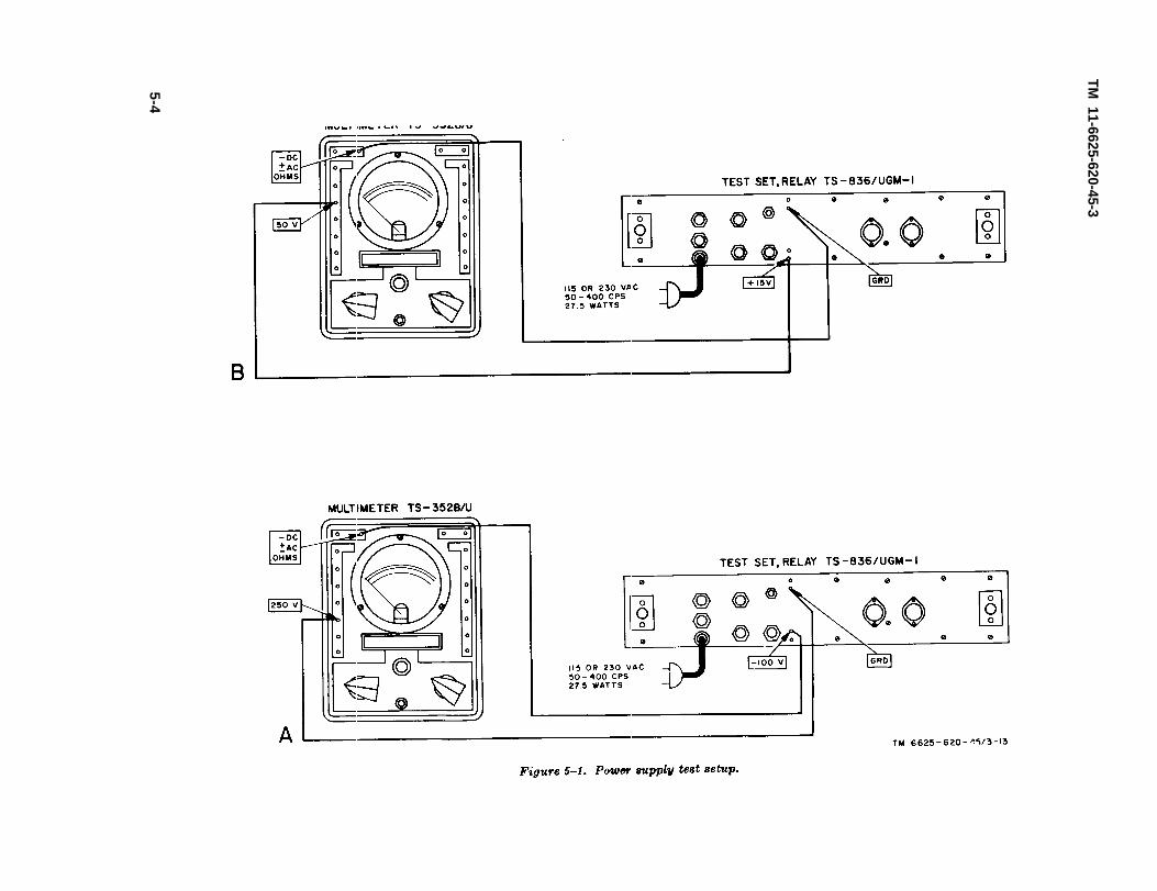
Figure 5-1.
TM 11-6625-620-45-3
5-4
TM
11-6625-620-45-3
Ch
an
ge
1
5
-5
TM 11-6625-620-45-3
5-6 Change 1
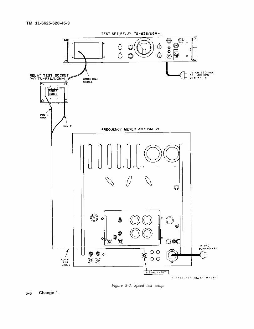
Figure 5-2. Speed test setup.

5-8. Speed Test
a. Test Equipment and Materials.(1) Frequency Meter AN/USM-2G.(2) Coexial test cable.(3) Solid stab relay, Type 9218
or Stelma Type ER-17A or ER21.b. Initial Test Equipment Calibration.There are no formal calibration procedures forthe AN/USM–26. However, calibration of theAN/USM–26 should be checked by perform-ing the following:
Caution: POWER switch S1 must be in theOFF (down) position before installing or re-moving a front panel plug-in unit.
(1)
(2)
(3)
(4)
Check to see that the front-panelplug-in is in plain.Operate the POWER switch to theON position. Allow for a 30-minutewarmup period. Do not make any con-nections to equipment during thistime.Operate the MANUAL GATE switchto the closed position.Operate the FUNCTION SELEC-TOR switch to the 100KC CHECKposition.
(5)
(6)
(7)
(8)
TM 11-6625-620-45-3
Adjust the DISPLAY TIME controlfor the desired display. The extremecounterclockwise position is usuallybest. (The display time cannot beadjusted to be less than gate time. )Check to see that the indication of thedisplay system for each position of theFREQUENCY UNIT switch agreeswith the values given in the chart.Set the FUNCTION SELECTORswitch to the 10MC CHECK position.Repeat (6) above, and allow a ± 1count in the last digit.
Counter readings for calibration check
10 0100.0000 0000.0000 ±.0011 00100.000 10000.000 ±.0010.1 000100.0 010000.00 ±.010.01 0000100.0 0010000.0 ±.010.001 00000100 00010000. ±1
c. Test Connections and Conditions. Removerelay test socket assembly 3A2 by unscrewingthe two captive screws on each side of the as-sembly, and then connect the equipment asshown in figure 5-2.
Change 1 5-7
Gate Time 100KC CHECK 10MC CHECK(seconds)
TM
11-6625-620-45-3
5-8 Change 1
TM
11-6625-620-45-3
Ch
an
ge
1
5
-9
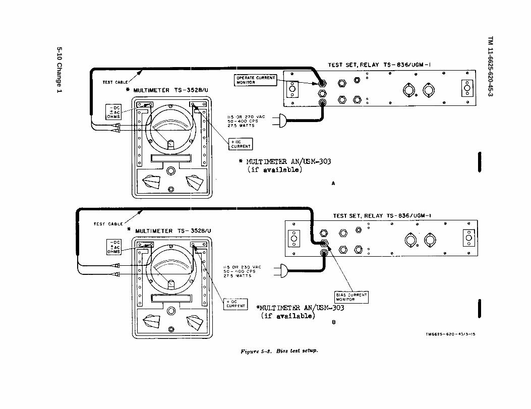
Figure 5-3.
TM 11-6625-620-45-3
5-10 Ch
ang
e 1

TM 11-6625-620-45-3
Ch
ang
e 1 5-11

TM
11-6625-620-45-3
15-17
Change

TM 11-6625-620-45-3
5-13. Summary of Performance Standards
Personnel may find it convenient to arrangethe checklist in a manner similar to that shownbelow.
TEST SET, RELAY TS-836/UGM-l
1. POWER SUPPLYTEST
a. J6 outputb. J8 outputc. J9 output
2. SPEED TESTa. Output frequencyb. Output frequencyc. Output frequencyd. Output frequencye. Output frequency
3. BIAS TESTa. Test set output
currentb. Test set output
currentc. Test set output
currentd. Test Set output
currente. Test set output
currentf. Test set output
current4. CONTACT EFFI-
CIENCY TESTStep No. 1
a. Relay testb. Relay test
- - - -- - - -- - - -
-------------------------- - - -
------
- - - -
-------
-------
--------
-------
-------
-100 volts ± 10%+100 volts ± 10%+15 volts ± 10%
43.44 ms ± 1%26.96 ms ± 1%13.33 ms ± 1%10.00 ms ± 1%8.00 m ± 1%
30 ma ± 5%
8 ma ± 5%
20 ma ± 5%
60 ma ± 5%
94 or higher92 or higher
TEST SET, RELAY TS-836/UGM-l
c. Relay testd. Relay to ----e. Relay test --—-
Step No. 2a. Relay test ----b. Relay test ---—c. Relay test ----d. Relay test ----c. Relay test ----
Step No. 3a. Relay test ----b. Relay test ----c. Relay test -----d. Relay test ----e. Relay test ----
5. CONTACT BOUNCETEST
Reversals pattern on -----OS-8 C/U
6. ELECTRONIC RELAYOPERATIONALTEST
a. TS-836/UGM-1 out-----------put
b. TS-1836/UGM-1 out-----put
c. TS-836/UGM-1 out- ----put
d. TS436/UGM-1 out- ----put
c. TS-836/UGM-1 out- ----put
f. TS-836/UGM-1 out- ----put
84 or higher79 or higher75 or higher
96 or higher95 or higher
890 or higher
8 or higher85 or higher
97 or higher96 or higher93 or higher91 or higher88 or higher
Verify
0 ma
Full-scaledeflection
A p p r o x . z e r o
A p p r o x . z e r o
A p p r o x . z e r o
A p p r o x . z e r o
5-18 Change 1
Testdata
Per f o rmancestandard
4 ma ± 5%
10 ma ± 5%
TestData
- - - - -
Performancestandard

TM 11-6625-620-45-3
T E S T S E T , R E L A Y T S - 8 3 6 / U G M - l
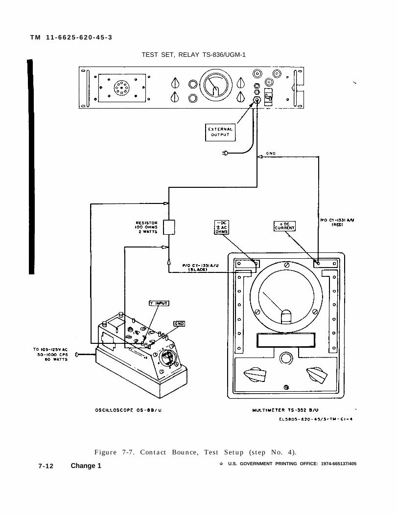
Figure 7 - 6 . Contact Bounce, Test Setup (steps no. 1, 2, and 3) .
Change 1 7-11
TEST SET, RELAY TS-836/UGM-1
7-12
Figure 7-7. Contact Bounce, Test Setup (step No. 4).
Change 1 U.S. GOVERNMENT PRINTING OFFICE: 1974-665137/405
T M 1 1 - 6 6 2 5 - 6 2 0 - 4 5 - 3


By Order of the Secretary of the Army:
CARL E. VUONOGeneral, United States Army
Chief of StaffOfficial:
R. L. DILWORTHBrigadier General, United States Army
The Adjutant General
Distribution:
To be distributed in accordance with DA Form 12-36,literature requirements for TS-836/UGM-1.
U.S. GOVERNMENT PRINTlNG OFFICE: 1991 - 281-523/46010


THE METRIC SYSTEM AND EQUIVALENTS

PIN: 020939-001