tip-enhanced spectroscopy and electron generation
TRANSCRIPT

Tip-Enhanced Spectroscopy and Electron Generation
Thomas ElsaesserMax-Born-Institute for Nonlinear Optics and Short-Pulse Spectroscopy,
D-12489 Berlin, Germany, http://www.mbi-berlin.de
• Sub-wavelength optics and nanoplasmonics
• Light scattering from metal nanotips
• Tip-enhanced spectroscopies
• Generation of ultrashort electron pulses
Tutorial Sonderforschungsbereich 658
Coauthors
Markus Raschke David Solli
Catalin Neacsu UC Los Angeles
Markus Breusing
Claus Ropers Dong Ha Kim
Christoph Lienau Wolfgang Knoll
Max-Born-Institute MPI Polymer Research Mainz

Optical spectroscopy allows for generation and observation of elementary excitations with well-defined properties.
Optics on a nanometer = sub-wavelength length scale for
• 'imaging' single nanoobjects
• studying spatio-temporal processes.
Ensemble of nanosystems: size fluctuations result in inhomogeneous broadening.
Motivation: Why optics on a sub-wavelength scale ?
Far-field microscopy:resolution Δx=0.61λ/NA >λ/5
Near-field microscopy:resolution λ/50 - λ/10

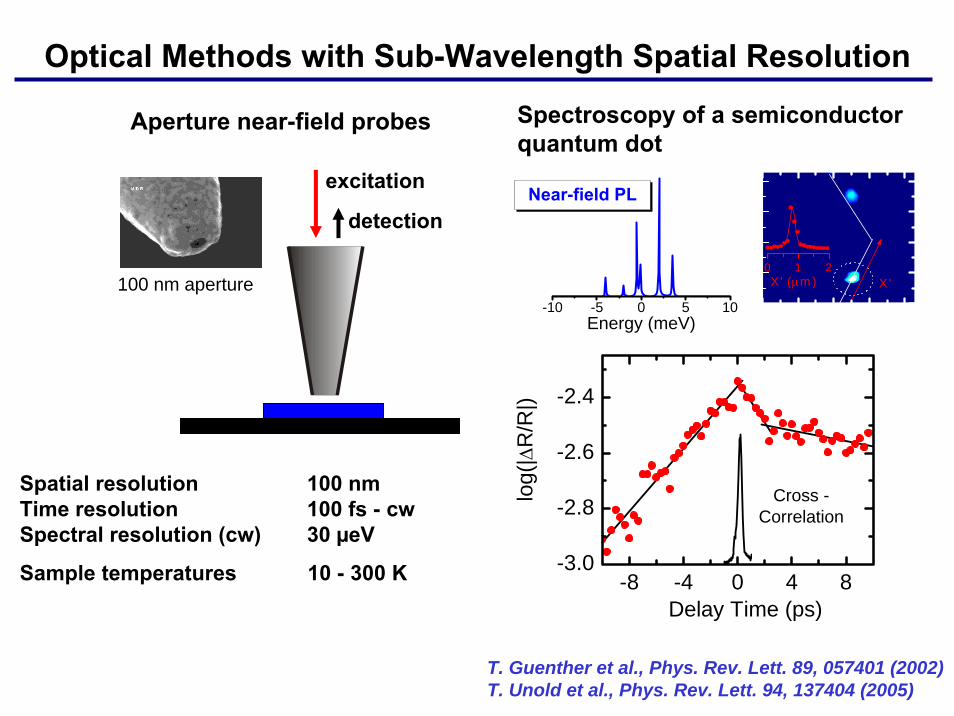
Optical Methods with Sub-Wavelength Spatial Resolution
Aperture near-field probes Apertureless scattering
scattered light
illumination
excitation
detection
100 nm aperture r=20 nm Au tip
Spatial resolution 100 nm 10 nmTime resolution 100 fs - cw 10 fs - cwSpectral resolution (cw) 30 µeV several meV
Sample temperatures 10 - 300 K 300 K
Other methods: Illumination of metallic slit and hole masks ('nanoplasmonics'),Stimulated emission depletion microscope (STED)
Optical Methods with Sub-Wavelength Spatial Resolution
Aperture near-field probes
excitation
detection
100 nm aperture
Spatial resolution 100 nmTime resolution 100 fs - cwSpectral resolution (cw) 30 µeV
Sample temperatures 10 - 300 K
Spectroscopy of a semiconductorquantum dot
0 1 2 3 4
X'
0 1 2X' (μm )
-8 -4 0 4 8-3.0
-2.8
-2.6
-2.4
Cross -Correlation
Delay Time (ps)
log(
|ΔR
/R|)
-10 -5 0 5 10Energy (meV)
Near-field PL
T. Guenther et al., Phys. Rev. Lett. 89, 057401 (2002)T. Unold et al., Phys. Rev. Lett. 94, 137404 (2005)

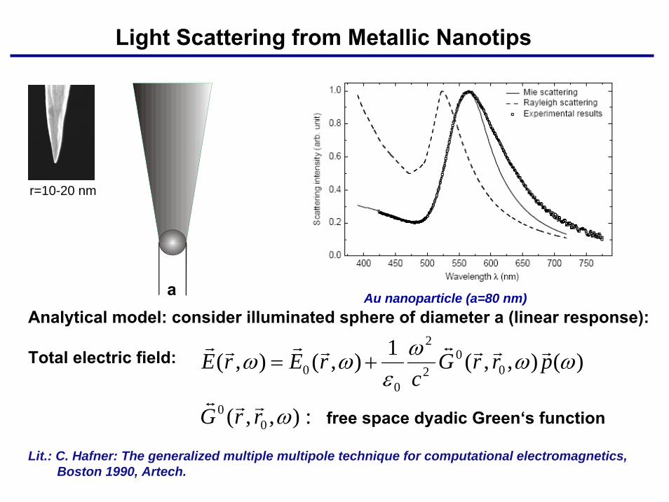
Light Scattering from Metallic Nanotips
a
r=10-20 nm
Scatterer dimension a=2r << λ(Mie scattering)
Electric field enhancement for field vector parallel to tip axis:
- lightning rod effect (field singularity at tip apex)
- surface plasmon excitation
Field enhancement factor 10 – 100
E E
Dielectric function of bulk metals:
Drude model (independent electrons)
Lindhard: interacting electrons, no collisions
)(1
)(1)( 2
02
02
20
2
2
0
2
γωωγω
γωω
γωωω
ωε+
++
−=+
−= ppp ii
∫ +−+
−+= +
ωππωε
hrvrrrr
)()(441),( 3
3
2
2
kEqkE
ffkdqeq kqk

Light Scattering from Metallic Nanotips
a
r=10-20 nm
Scatterer dimension a=2r << λ Numerically calculated intensity distribution(Mie scattering)
Electric field enhancement for field vector parallel to tip axis:
- lightning rod effect (field singularity at tip apex)
- surface plasmon excitation
Field enhancement factor 10 – 50 L. Novotny et al., Phys. Rev. Lett. 79, 645 (1997),Annu. Rev. Phys. Chem. 57, 303 (2006)
E E

Light Scattering from Metallic Nanotips
a
r=10-20 nm
Scatterer dimension a=2r << λ Induced surface charge density(Mie scattering)
Surface plasmon excitation:
- Calculate induced surface charge density and electric field from Maxwell‘sequations by multiple multipole method (MMP)
- Standing wave of oscillating surface charge with wavelength smaller thanoptical wavelength
L. Novotny et al., Phys. Rev. Lett. 79, 645 (1997)
E E

Light Scattering from Metallic Nanotips
a
r=10-20 nm
Au tip Au sphereAnalytical model: consider illuminated sphere of diameter a (linear response):
λlight=810 nm, Au sphere r0=10 nm: ε=-24.9+1.57i , fe=-2.9+11.8i
E
)(00
0000
)( ωα
αα
ω light
par
pp
pp
Eprr
⎥⎥⎥
⎦
⎤
⎢⎢⎢
⎣
⎡
=
)(8
2)(1)(4
300
300
ωπεα
ωεωεπεα
epar
pp
fr
r
=
+−
=

Light Scattering from Metallic Nanotips
a
r=10-20 nm
Au nanoparticle (a=80 nm)Analytical model: consider illuminated sphere of diameter a (linear response):
E
)(00
0000
)( ωα
αα
ω light
par
pp
pp
Eprr
⎥⎥⎥
⎦
⎤
⎢⎢⎢
⎣
⎡
=
)(8
2))(Re(,:
2)(1)(4
300
*0
2
300
ωπεα
ωεε
ω
ωεωεπεα
epar
pp
pp
fr
mNeplasmon
r
=
−==
+−
=
Light Scattering from Metallic Nanotips
a
r=10-20 nm
E
Au nanoparticle (a=80 nm)Analytical model: consider illuminated sphere of diameter a (linear response):
Total electric field:
free space dyadic Green‘s function
Lit.: C. Hafner: The generalized multiple multipole technique for computational electromagnetics,Boston 1990, Artech.
:),,(
)(),,(1),(),(
00
00
2
2
00
ω
ωωωε
ωω
rrG
prrGc
rErE
rrt
rrrtrrrr+=
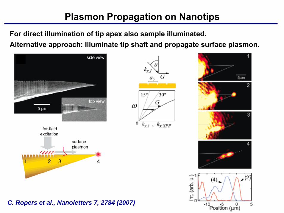
Plasmon Propagation on NanotipsFor direct illumination of tip apex also sample illuminated.Alternative approach: Illuminate tip shaft and propagate surface plasmon.
C. Ropers et al., Nanoletters 7, 2784 (2007)
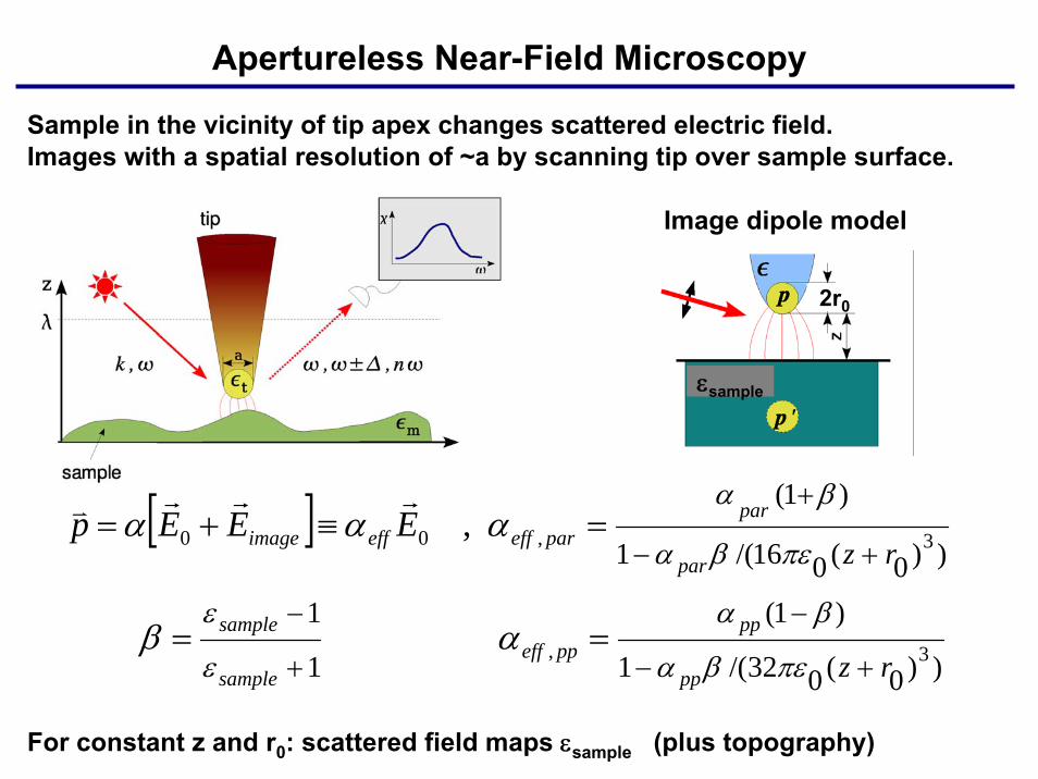
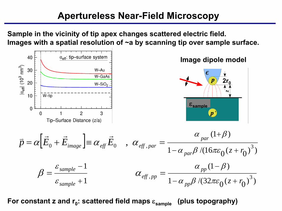
Apertureless Near-Field Microscopy
Sample in the vicinity of tip apex changes scattered electric field.Images with a spatial resolution of ~a by scanning tip over sample surface.
Image dipole model
[ ]
))0(032/(1
)1(
1
1
))0(016/(1
)1(
3,
3,00 ,
rz
rz
pp
ppppeff
sample
sample
par
parpareffeffimage EEEp
+−
−
+
−
+−
+
==
=≡+=
πεβα
βα
ε
ε
πεβα
βα
αβ
αααrrrv
2r0
εsample
For constant z and r0: scattered field maps εsample (plus topography)

Experimental Setup
100 nm
W
0.2 mm
Au (r=20 nm)
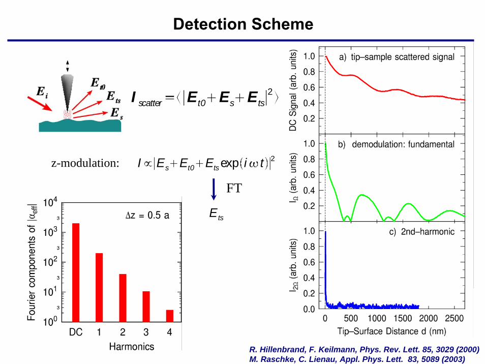
Detection Scheme
I scatter Et0 Es Ets2
I Es Et0 Etsexp i t 2
Ets
z-modulation:
FT
R. Hillenbrand, F. Keilmann, Phys. Rev. Lett. 85, 3029 (2000)M. Raschke, C. Lienau, Appl. Phys. Lett. 83, 5089 (2003)
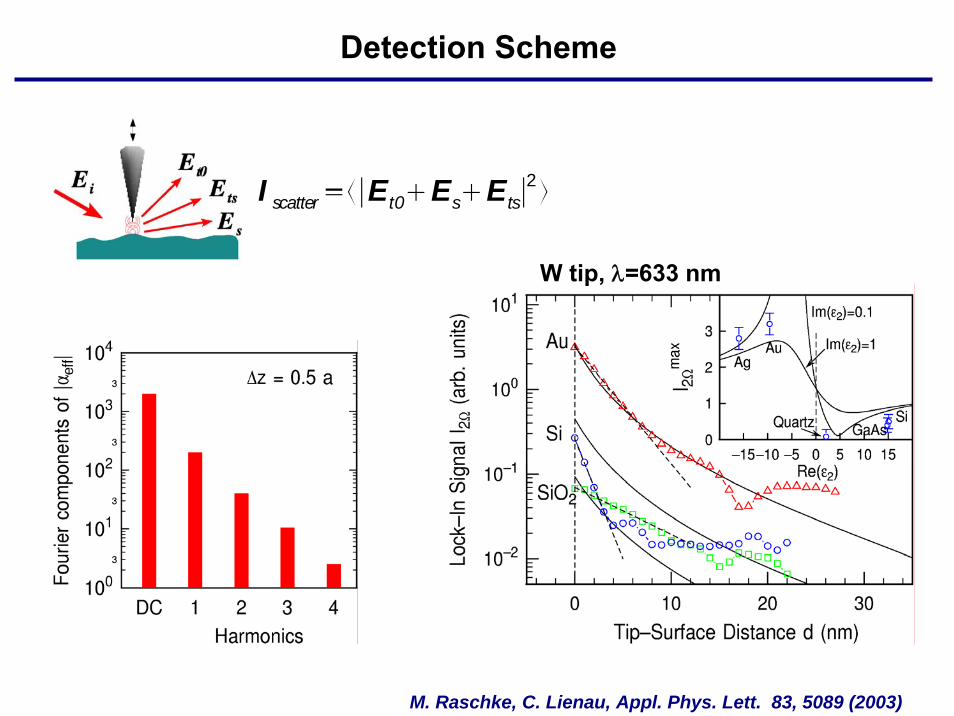
Detection Scheme
I scatter Et0 Es Ets2
M. Raschke, C. Lienau, Appl. Phys. Lett. 83, 5089 (2003)
W tip, λ=633 nm

Detection Scheme
I scatter Et0 Es Ets2
M. Raschke, C. Lienau, Appl. Phys. Lett. 83, 5089 (2003)
W tipsλ=633 nm
r 12 nm
r 20 nm
r 5 nm

Chemical composition and structure on the nano-scale.
Raman scattering:
Field enhancement at tip apex enhances Ramanscattered field (plasmon resonance).
In addition possible: enhancement of αij by electronicresonance of sample.
Detection of Stokes and/or anti-Stokes component.
Infrared absorption:
Vibrational resonances contribute to εsample.
Requires (tunable) infrared light.
Nonlinear and time-resolved Raman and infrared spectroscopies possible.
Stokes
Tip-Enhanced Vibrational Spectroscopy
ωLaserω
v=0
v=1
v=2
VibLaserStokes ωωω −=
n
N
n n
ijijij q
qEP
0
63
1)0(, ∑
−
=⎥⎦
⎤⎢⎣
⎡∂
∂+==
αααα
rr
n
N
n na q
qµµµiref
0
63
1
2)0(, ∑
−
=⎥⎦
⎤⎢⎣
⎡∂∂
+=∝rrσ

Single-walled carbon nanotubes (SWN) on glass.
Tip-Enhanced Raman Spectroscopy
StokesωLaserω
Topography 1594 cm-1 vibration
resolution
L. Novotny et al.

Single walled carbon nanotubes (SWN) on glass.
Tip-Enhanced Raman Spectroscopy
StokesωLaserω
Topography 1594 cm-1 vibration
resolution
L. Novotny et al.
Raschke et al.: malachite green (MG)

Polystyrene – b – Polyvinylpyridine film: λ=3,39 µm (CH stretch vibration)
Topography: Microscopy
Tip-Enhanced Infrared Spectroscopy
s-SNOM:
vis 632nm
M. Raschke et al., ChemPhysChem. 6, 2197 (2005)

Tip-Enhanced Infrared Spectroscopy
M. Raschke et al., ChemPhysChem. 6, 2197 (2005)

Other Tip-Enhanced Spectroscopies
Local photoluminescence emission
PL, λ=950 nm Raman 1594 cm-1
A. Hartschuh et al., Nanoletters 5, 2310 (2005)
Variation of spectra along nanotube
Also demonstrated: second harmonic spectroscopy

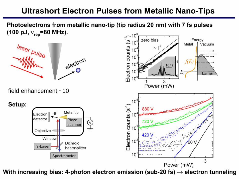
Ultrashort Electron Pulses from Metallic Nano-TipsPhotoelectrons from metallic nano-tip (tip radius 20 nm) with 7 fs pulses(100 pJ, νrep=80 MHz).
field enhancement ~10
Setup:
scattered 800 nm light
2nd harmonic (400 nm)
electrons
C. Ropers et al, Phys. Rev. Lett. 98, 043907 (2007)
Ultrashort Electron Pulses from Metallic Nano-TipsPhotoelectrons from metallic nano-tip (tip radius 20 nm) with 7 fs pulses(100 pJ, νrep=80 MHz).
field enhancement ~10
Setup:
scattered 800 nm light
2nd harmonic (400 nm)
electrons
With increasing bias: 4-photon electron emission (sub-20 fs) → electron tunneling
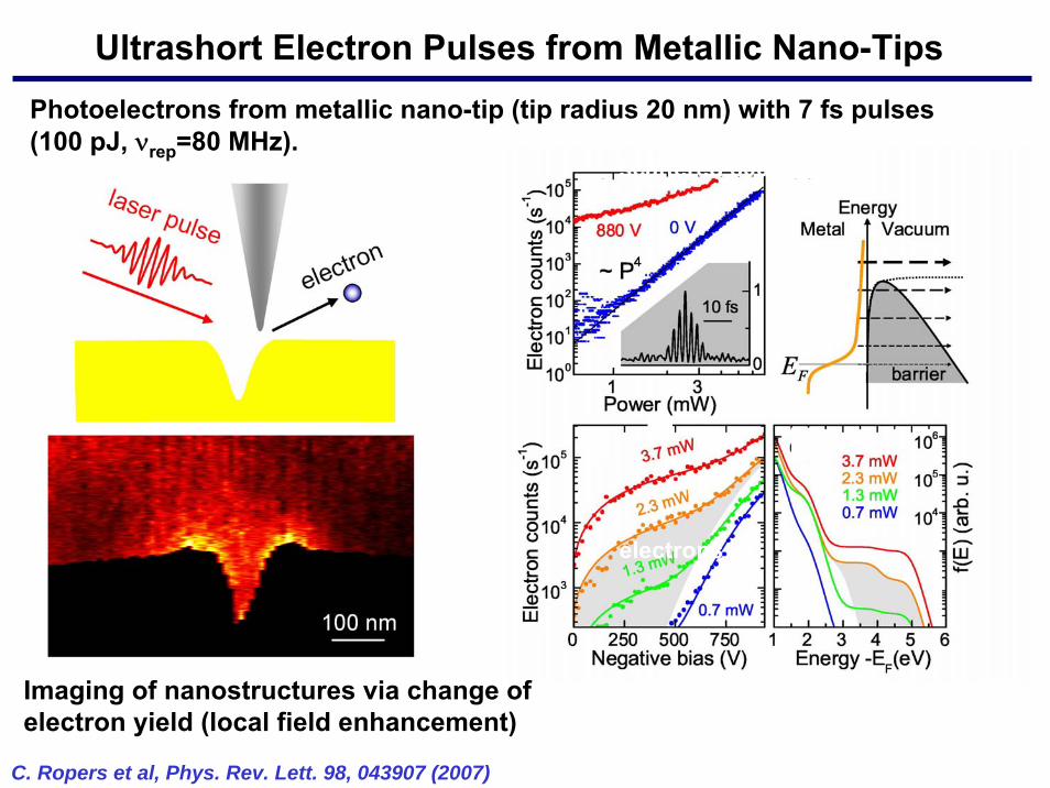
Ultrashort Electron Pulses from Metallic Nano-TipsPhotoelectrons from metallic nano-tip (tip radius 20 nm) with 7 fs pulses(100 pJ, νrep=80 MHz).
scattered 800 nm light
electrons
Imaging of nanostructures via change ofelectron yield (local field enhancement)
C. Ropers et al, Phys. Rev. Lett. 98, 043907 (2007)

Conclusions
Apertureless tip-enhanced microscopies allow for optical experimentswith a 10 nm spatial resolution.
Variety of linear and nonlinear spectroscopies to study electronic andvibrational excitations.
Sensitivity up to the single-molecule level.
‚Point-like‘ source of femtosecond electron pulses by multiphoton excitationof metallic tips.
Future developments:
Time-resolved spectroscopies, in particular in the ultrafast time domain.
Electron scattering and diffraction experiments.