tightbinding modelling of semiconductor...
TRANSCRIPT
Tightbinding Modelling of
Semiconductor Nanowires
ME 346
Stanford University
November 14, 2004
Paul Leu ([email protected])Instructor: Prof. Wei Cai ([email protected])
1
1 Background
Semiconducting nanowires are a promising nanomaterial in that their geometric and electrical
properties can be well-controlled during their synthesis. Semiconducting nanowires can be doped
to vary the concentration of carriers. Boron doped and phosphorus doped silicon nanowires have
been shown to behave as p-type and n-type materials respectively [1]. In addition, the diameters
of semiconducting nanowires are determined by the size of the metal catalyst nanoparticles from
which they grow [2, 3]. Nanowire length has been shown to correlate linearly with growth time
[4] and also depend linearly on the size of the nanoparticles from which they grow [5]. A large
variety of nanowires materials including Si, Ge, GaN, InP, and ZnO can be synthesized [6], and
many semiconductor industry techniques can be used with nanowires.
The levels of physical and chemical control possible during synthesis suggests the emer-
gence of semiconductor nanowires for a wide variety of possible nanowire applications. Silicon
nanowires have been demonstrated to only allow electron flow in one direction and could also
be used to create bipolar transistors and complementary inverters [7]. Field effect transistors
(FET) and p-n diodes have been assembled out of GaN [8] and InP [9] by forming a p-n junction
with a n-type GaN or InP and p-type SiNWs. The junctions with InP, in fact, are photolumi-
nescent, behaving as nanoscale light emitting diodes. Sensors are also feasible as boron-doped
Si nanowire surfaces have been modified with molecular receptors to make them sensitive to pH,
streptavidin, antibodies, and Ca2+ [10]. Nanowires have also been functionalized with redox
active molecules and assembled using fluidic-flow directed approaches to form programmable
logic arrays [11]. Optical applications are also a possibility as ZnO nanowires were recently
shown to exhibit a lasing action under optical excitation [12]. ZnO nanowires can also be used
to guide light, similar to optical fiber.
2 Motivation
The purpose of this project is to characterize the bandgap and transport characteristics of
semiconductor nanowires using tight-binding simulations, which can handle up to a few thousand
atoms. We aim to determine size and shape effects of semiconductor nanowires on their electronic
2
properties.
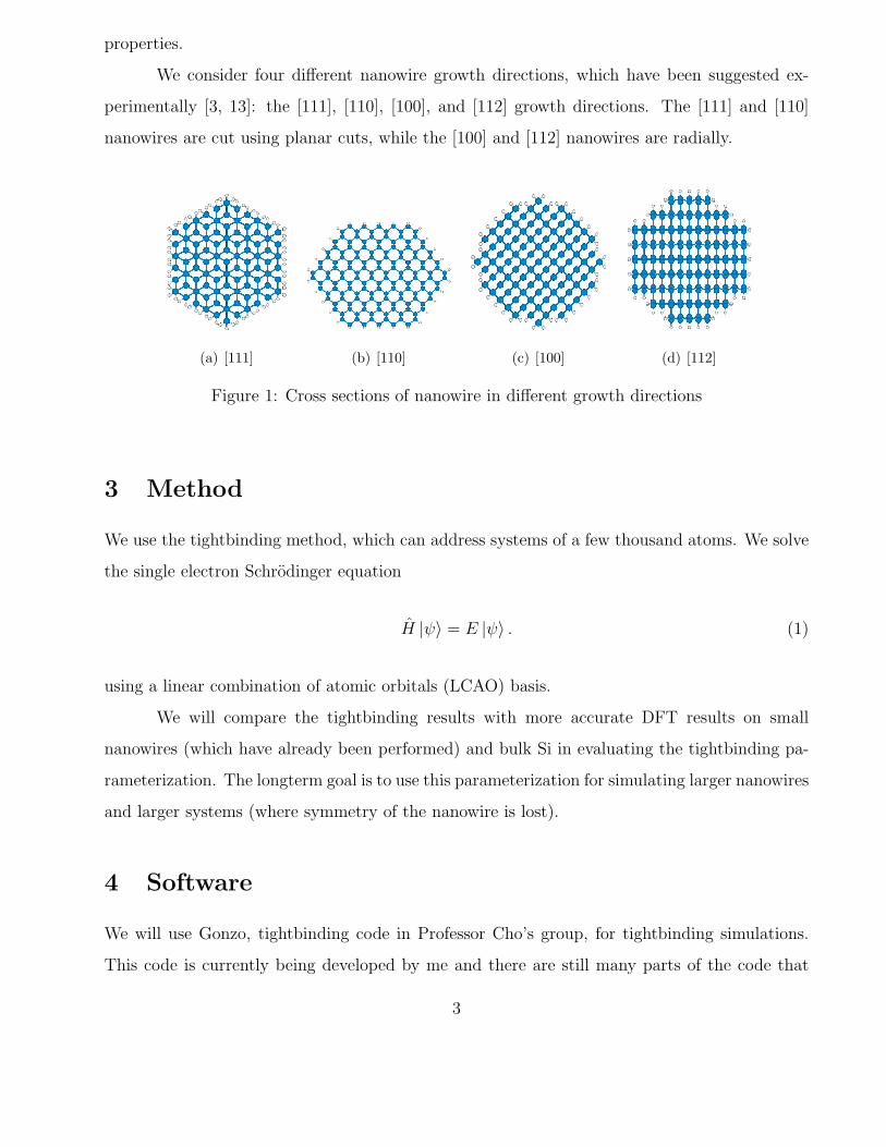
We consider four different nanowire growth directions, which have been suggested ex-
perimentally [3, 13]: the [111], [110], [100], and [112] growth directions. The [111] and [110]
nanowires are cut using planar cuts, while the [100] and [112] nanowires are radially.
(a) [111] (b) [110] (c) [100] (d) [112]
Figure 1: Cross sections of nanowire in different growth directions
3 Method
We use the tightbinding method, which can address systems of a few thousand atoms. We solve
the single electron Schrodinger equation
H |ψ〉 = E |ψ〉 . (1)
using a linear combination of atomic orbitals (LCAO) basis.
We will compare the tightbinding results with more accurate DFT results on small
nanowires (which have already been performed) and bulk Si in evaluating the tightbinding pa-
rameterization. The longterm goal is to use this parameterization for simulating larger nanowires
and larger systems (where symmetry of the nanowire is lost).
4 Software
We will use Gonzo, tightbinding code in Professor Cho’s group, for tightbinding simulations.
This code is currently being developed by me and there are still many parts of the code that
3

are untested or still need refinement.
5 Time Table
Table 1:
week # goals
1 Simulate bulk Si and smallest nanowire2 Fix parameterization3 Simulate larger nanowires
References
[1] Y. Cui, X. Duan, J. Hu, and C.M. Lieber. Doping and electrical transport in siliconnanowires. The Journal of Physical Chemistry B, 104(22):5213–5216, June 8 2000.
[2] M.S. Gudiksen and C.M. Lieber. Diameter selective synthesis of semiconductor nanowires.Journal of the American Chemical Society, 122:8801–8802, 2000.
[3] Y. Cui, L.J. Lauhon, M.S. Gudiksen, J. Wang, and C.M. Leiber. Diameter-controlledsynthesis of single-crystal silicon nanowires. Applied Physics Letters, 78(15):2214–2216,April 9 2001.
[4] M. S. Gudiksen, J. Wang, and C. M. Lieber. Synthetic control of the diameter and length ofsingle crystal semiconductor nanowires. Journal of Physical Chemistry B, 105:4062–4064,2001.
[5] Y. Wu, R. Fong, and P. Yang. Block-by-block growth of single-crystalline Si/SiGe super-lattice nanowires. Nano Letters, 2(2):83–86, 2002.
[6] X. Duan and C.M. Leiber. General synthesis of compound semiconductor nanowires. Ad-
vanced Materials, 12(4):298–302, 2000.
[7] Y. Cui and C.M. Leiber. Functional nanoscale electronic devices assembled using siliconnanowire building blocks. Science, 291:851–853, February 2 2001.
[8] Y. Huang, X. Duan, Y. Cui, and C.M. Lieber. Gallium nitride nanowire nanodevices. Nano
Letters, 2(2):101–104, 2002.
[9] X. Duan, Y. Huang, Y. Cui, J. Wang, and C.M. Leiber. Indium phosphide nanowiresas building blocks for nanoscale electronic and optoelectronic devices. Nature, 409:66–69,January 4 2001.
4
[10] Y. Cui, Q. Wei, H. Park, and C.M. Lieber. Nanowire nanosensors for highly-sensitive,selective and integrated detection of biological and chemical species. Science, 293:1289–1292, 2001.
[11] X. Duan, Y. Huang, and C.M. Leiber. Nonvolatile memory and programmable logic frommolecule-gate nanowires. Nano Letters, 2(5):487–490, 2002.
[12] M.H. Huang, S. Mao, H. Feick, H. Yan, Y. Wu, H. Kind, E. Weber, R. Russo, and P. Yang.Room-temperature ultraviolet nanowire nanolasers. Science, 292(5523):1897–1899, June 82001.
[13] D. D. D. Ma, C. S. Lee, F. C. K. Au, S. Y. Tong, and S. T. Lee. Small-diameter siliconnanowire surfaces. Science, 299:1874–1877, March 21 2003.
5