three-level anpc
DESCRIPTION
Loss balacing in a three-level ANPCTRANSCRIPT

Faculty of Engineering and ScienceInstitute of Electronic SystemsFredrik Bajers Vej 7 A19220 Aalborg ØDenmarkhttp://ies.aau.dk
Synopsis:This project concerns the development of acamera system for taking a picture of Earthfrom a CubeSat. Based on a market survey, asuitable image sensor complying with the re-quirements for operation in space is chosen.For testing purposes, a lens is chosen, but acomprehensive market survey should be madeto select a lens suitable for operation in space.The functionality of the camera system is an-alyzed using UML use cases. The use casesobtained are take picture, generate thumbnail,and self test.In order to test the camera system, a testsystem is constructed, based on the Motorola68000. The test system runs the TS2MONdebugger/monitor and communicates with aPC over a RS232 connection. This forms aplatform for designing the interfaces needed forthe camera. Hardware and software design ofthe camera system is modulated by using theuse cases and the Rugby metamodel.The hardware and software of the test systemworks as designed, but it has not been possibleto take a picture. It is possible to communi-cate with the camera, but the resulting datadoes not resemble a picture. This is possiblydue to misconguration of the camera. Dur-ing software integration, faulty memory readshave occurred, which are believed to be EMCrelated, due to the long buses. Both of theseproblems are not investigated further, whichshould be done before the camera can be usedon board a CubeSat.
Title:Low cost camera for CubeSats a feasibility study
Theme:Microcomputer systems
Project period:E4, spring semester 2006
Project group:418
Group members:Simon Just Kjeldgaard PedersenMorten Burchard TychsenMorten Egelund JensenJens Martin Oddershede
Supervisor:Rasmus Abildgren
Number printed:7
Number of pages:Report: 95Appendicies: 42Total: 137
Finished:29th May 2006
Institute of Energy Technology
Loss Balancing in a Three Level
Active Neutral Point Clamped
Converter
pwm-df-r.jpg
- 2010 -


Title: Loss Balancing in a Three Level Active Neutral Point Clamped ConverterSemester: 8Semester theme: Control in converter-fed AC drivesProject period: 15.02.2010 - 26.05.2010ECTS: 26Supervisor: Andrzej AdamczykProject group: 840
Catalin Dincan
Cam Pham
Claudia Georgiana Cojocaru
Marco Guarrera
SYNOPSIS
An unbalanced distribution of the semiconductor powerlosses amongst the switches of a converter will limit itsswitching frequency and output power. Hence, for theNeutral Point Clamped (NPC) topology, which is widelyused in medium voltage, high power drives, this issuerepresents a major disadvantage. In order to overcomethis drawback, the NPC can be replaced by the ActiveNeutral Point Clamped (ANPC) topology.This report investigates different modulations strategieswhich can be used for controlling the ANPC converterin order to balance the power losses amongst the semi-conductor devices.Several strategies, which use the active neutral pointclamping switches are presented and analysed throughsimulations and experimental tests.The obtained results confirm that by taking advantageof the flexibility provided by ANPC topology, a majorimprovement in the losses distribution can be brought.
Copies: 2Pages: 85Appendices: 4Supplements: 1 CD
By signing this document, each member of the group confirms that all partic-ipated in the project work and thereby all members are collectively liable forthe content of the report.


Title: Jvn fordeling af tab i en three-level ANPCSemester: 8Semester theme: Styring af konverter til at forsyne AC driverProject period: 15.02.2010 - 26.05.2010ECTS: 26Supervisor: Andrzej AdamczykProject group: 840
Catalin Dincan
Cam Pham
Claudia Georgiana Cojocaru
Marco Guarrera
SYNOPSIS
En ujvn fordeling af effekt tabene imellem konvert-erens kontaktorer vil begrnse dens switchs frekvens ogudgangseffekt. Deraf, for Neutral Point Clamped (NPC)topologi, som er anvendt i stor udstrkning i mellemsp-nding, hj effekt driver, denne problemstilling er hoved-sagelig den vigtigste ulempe. For at kunne lse denneulempe, NPC kan erstattes med den Aktiv Neutral PointClamped (ANPC) topologi.Denne rapport undersges hvilken modulation princip-per som kan bruges til at styre ANPC konverteren medhenblik i jvn fordeling af effekt tab imellem halvlederkomponenter.Flere principper som bruges af ANPC kontaktorer erfremlagt og analyseret gennem simulering og eksperi-menter.De opnet resultater bekrfter, ved at udnytte fleksibilitetgivet af ANPC topologi, forbedring af tabene fordelingkan hentes.
Oplag: 2Antal sider: 85Appendiks: 4Bilag: 1 CD
Ved at underskrive dette dokument bekrfter hvert enkelt gruppemedlem, atalle har deltaget ligeligt i projektarbejdet og at alle er kollektivt ansvarlige forrapportens indhold.


Preface
This report represents the documentation of the project entitled Loss Balancing in aThree Level Active Neutral Point Clamped Converter.
The project was prepared between the 15th of February and the 26th of May 2010, atAalborg University Institute of Energy Technology, by the 8th semester group 840.
The aim of the project was to study different modulation strategies for a three level ActiveNeutral Point Clamped (ANPC) inverter, in order to ensure loss equalization amongst thesemiconductor switches.
The report is structured into five chapters. The first chapter gives a brief presentationof the background an motivation for this project, setting the main objectives and limita-tions. Chapter two provides information about the theoretical concepts which are usedthroughout the report. In chapter three, Matlab Simulink simulations are performed inorder to study how the ANPC inverter behaves for different modulation strategies, fromthe point of view of losses distribution amongst the switches. In chapter four experimentalare performed in order verify if loss balancing is achieved. The final chapter presents theconclusions of the report and future work.
The literature references are shown in square brackets by numbers. The list of the refer-ences is presented in the chapter Bibliography. Appendices are assigned with letters, andarranged in alphabetical order at the end of the report. Figures and tables are numberedin the following format: Figure Chapter.Number and Table Chapter.Number.
The contents of the enclosed CD are listed in Appendix D.
26th of May 2010


Contents
1 Introduction 17
1.1 Background and motivation . . . . . . . . . . . . . . . . . . . . . . . . . . . 17
1.2 Problem formulation . . . . . . . . . . . . . . . . . . . . . . . . . . . . . . . 18
1.2.1 Project objectives . . . . . . . . . . . . . . . . . . . . . . . . . . . . 18
1.2.2 Project limitations . . . . . . . . . . . . . . . . . . . . . . . . . . . . 18
2 Basics on converter losses and the ANPC topology 19
2.1 IGBT and diode power losses . . . . . . . . . . . . . . . . . . . . . . . . . . 19
2.1.1 IGBT conduction losses . . . . . . . . . . . . . . . . . . . . . . . . . 19
2.1.2 IGBT switching losses . . . . . . . . . . . . . . . . . . . . . . . . . . 20
2.1.3 Diode losses . . . . . . . . . . . . . . . . . . . . . . . . . . . . . . . . 20
2.2 The Active Neutral Point Clamped topology . . . . . . . . . . . . . . . . . 21
2.2.1 Basics on three level converters . . . . . . . . . . . . . . . . . . . . . 21
2.2.2 ANPC topology . . . . . . . . . . . . . . . . . . . . . . . . . . . . . 23
2.2.3 Modulation strategies . . . . . . . . . . . . . . . . . . . . . . . . . . 24
2.3 Summary . . . . . . . . . . . . . . . . . . . . . . . . . . . . . . . . . . . . . 35
3 Simulations 37
3.1 System description . . . . . . . . . . . . . . . . . . . . . . . . . . . . . . . . 37
3.2 Simulation results . . . . . . . . . . . . . . . . . . . . . . . . . . . . . . . . 39
3.2.1 PWM-1 . . . . . . . . . . . . . . . . . . . . . . . . . . . . . . . . . . 39
3.2.2 PWM-2 . . . . . . . . . . . . . . . . . . . . . . . . . . . . . . . . . . 40
3.2.3 PWM-3 . . . . . . . . . . . . . . . . . . . . . . . . . . . . . . . . . . 41
3.2.4 PWM-DF . . . . . . . . . . . . . . . . . . . . . . . . . . . . . . . . . 42
3.2.5 PWM-ALD . . . . . . . . . . . . . . . . . . . . . . . . . . . . . . . . 43
3.2.6 Results for validation in the laboratory . . . . . . . . . . . . . . . . 44
3.3 Summary . . . . . . . . . . . . . . . . . . . . . . . . . . . . . . . . . . . . . 46
5

4 Laboratory implementation 49
4.1 Test setup . . . . . . . . . . . . . . . . . . . . . . . . . . . . . . . . . . . . . 49
4.1.1 ANPC converter . . . . . . . . . . . . . . . . . . . . . . . . . . . . . 50
4.1.2 DSP board . . . . . . . . . . . . . . . . . . . . . . . . . . . . . . . . 51
4.1.3 Interface board . . . . . . . . . . . . . . . . . . . . . . . . . . . . . . 51
4.2 Modulation implementation on the DSP . . . . . . . . . . . . . . . . . . . . 52
4.3 Experimental results . . . . . . . . . . . . . . . . . . . . . . . . . . . . . . . 53
4.3.1 R load . . . . . . . . . . . . . . . . . . . . . . . . . . . . . . . . . . . 53
4.3.2 RL load . . . . . . . . . . . . . . . . . . . . . . . . . . . . . . . . . . 58
4.4 Summary . . . . . . . . . . . . . . . . . . . . . . . . . . . . . . . . . . . . . 63
5 Conclusions 65
5.1 Review of the main tasks . . . . . . . . . . . . . . . . . . . . . . . . . . . . 65
5.2 Future work . . . . . . . . . . . . . . . . . . . . . . . . . . . . . . . . . . . . 66
Bibliography 69
A Heat sink selection 71
B Extension interface board 77
C List of used laboratory instruments 79
D Contents of the enclosed CD 81
6

List of Figures
1.1 Single-phase three-level NPC (a) and ANPC (b) voltage source converters . 17
2.1 Single-phase two-level half bridge (HB) (a) and three-level Neutral PointClamped (NPC) (b) voltage source converters . . . . . . . . . . . . . . . . . 21
2.2 Switching states for the single-phase three-level NPC converter: (a) P - S1
and S3 are on; (b) N - S4 and S6 are on; (c) O - S3 and S4 are on . . . . . 22
2.3 Single-phase ANPC voltage source converter . . . . . . . . . . . . . . . . . . 23
2.4 Switching states for the single-phase three-level ANPC converter: (a) P -S1 and S3 are on; (b) N - S4 and S6 are on; (c) OU - S2 and S3 are on; (b)OD - S4 and S5 are on; . . . . . . . . . . . . . . . . . . . . . . . . . . . . . . 24
2.5 PWM generation for the PWM-NPC strategy . . . . . . . . . . . . . . . . . 26
2.6 The switching sequences and output voltage for the PWM-NPC strategy.Because the frequency of the carrier waves is much higher than that of thereference signal, during one period of the carrier wave, the reference can beconsidered to be constant. . . . . . . . . . . . . . . . . . . . . . . . . . . . . 26
2.7 The switching sequences and output voltage for the 3L-ANPC PWM-1strategy. Because the frequency of the carrier waves is much higher thanthat of the reference signal, during one period of the carrier wave, the ref-erence can be considered to be constant. . . . . . . . . . . . . . . . . . . . . 27
2.8 The switching sequences and output voltage for the 3L-ANPC PWM-2strategy . . . . . . . . . . . . . . . . . . . . . . . . . . . . . . . . . . . . . . 28
2.9 PWM generation for the PWM-3 strategy . . . . . . . . . . . . . . . . . . . 29
2.10 Switching signals for the ANPC inverter switches with PWM-3 modulationstrategy . . . . . . . . . . . . . . . . . . . . . . . . . . . . . . . . . . . . . . 30
2.11 PWM generation for the PWM-DF strategy . . . . . . . . . . . . . . . . . . 31
2.12 The switching sequences and output voltage for the 3L-ANPC PWM-DFstrategy . . . . . . . . . . . . . . . . . . . . . . . . . . . . . . . . . . . . . . 31
2.13 PWM generation for PWM-ALD modulation strategy for 50%-50% StressIn/Stress Out ratio . . . . . . . . . . . . . . . . . . . . . . . . . . . . . . . . 33
2.14 The switching sequences and output voltage for the 3L-ANPC PWM-ALDstrategy . . . . . . . . . . . . . . . . . . . . . . . . . . . . . . . . . . . . . . 34
3.1 The general block diagram of the simulation models . . . . . . . . . . . . . 37
3.2 The PLECS block diagram of the plant . . . . . . . . . . . . . . . . . . . . 38
7

3.3 The Simulink block diagram of the losses calculation block . . . . . . . . . . 39
3.4 Power losses distribution for PWM-1 modulation strategy with a 10 kWload (PF = 1) . . . . . . . . . . . . . . . . . . . . . . . . . . . . . . . . . . . 40
3.5 Power losses distribution for PWM-2 modulation strategy with a 10 kWload (PF = 1) . . . . . . . . . . . . . . . . . . . . . . . . . . . . . . . . . . . 41
3.6 Power losses distribution for PWM-3 modulation strategy with a 50%-50%PWM-1/PWM-2 ratio and a 10 kW load (PF = 1) . . . . . . . . . . . . . . 42
3.7 Power losses distribution for PWM-DF modulation strategy with a 10 kWload (PF = 1) . . . . . . . . . . . . . . . . . . . . . . . . . . . . . . . . . . . 43
3.8 Power losses distribution for PWM-ALD modulation strategy with a 50%-50% Stress In/Stress Out ratio and a 10 kW RL load (PF = 0,85) . . . . . 44
4.1 Block diagram of the experimental test setup . . . . . . . . . . . . . . . . . 49
4.2 Laboratory test setup: (1)- 300 V, 5 A DC power supply; (2)- 24 V, 3 ADC power supply; (3)- single-phase ANPC converter; (4)- load resistor; (5)-load inductor; (6)- thermal camera; (7)- single-phase power analyser; (8)-TMS320F28335 eZdsp board; (9)- interface board; (10)- oscilloscope; (11)-PC . . . . . . . . . . . . . . . . . . . . . . . . . . . . . . . . . . . . . . . . . 50
4.3 Simulink model used for DSP implementation . . . . . . . . . . . . . . . . . 52
4.4 Thermal picture of the ANPC inverter with R load for PWM-1 modulationstrategy . . . . . . . . . . . . . . . . . . . . . . . . . . . . . . . . . . . . . . 54
4.5 Thermal picture of the ANPC inverter with R load for PWM-2 modulationstrategy . . . . . . . . . . . . . . . . . . . . . . . . . . . . . . . . . . . . . . 55
4.6 Thermal picture of the ANPC inverter with R load for PWM-3 modulationstrategy . . . . . . . . . . . . . . . . . . . . . . . . . . . . . . . . . . . . . . 56
4.7 Thermal picture of the ANPC inverter with R load for PWM-DF modula-tion strategy . . . . . . . . . . . . . . . . . . . . . . . . . . . . . . . . . . . 57
4.8 Thermal picture of the ANPC inverter with R load for PWM-ALD modu-lation strategy . . . . . . . . . . . . . . . . . . . . . . . . . . . . . . . . . . 58
4.9 Thermal picture of the ANPC inverter with RL load for PWM-1 modulationstrategy . . . . . . . . . . . . . . . . . . . . . . . . . . . . . . . . . . . . . . 59
4.10 Thermal picture of the ANPC inverter with RL load for PWM-2 modulationstrategy . . . . . . . . . . . . . . . . . . . . . . . . . . . . . . . . . . . . . . 59
4.11 Thermal picture of the ANPC inverter with RL load for PWM-3 modulationstrategy . . . . . . . . . . . . . . . . . . . . . . . . . . . . . . . . . . . . . . 60
4.12 Thermal picture of the ANPC inverter with RL load for PWM-DF modu-lation strategy . . . . . . . . . . . . . . . . . . . . . . . . . . . . . . . . . . 60
4.13 Thermal picture of the ANPC inverter with RL load for PWM-ALD mod-ulation strategy . . . . . . . . . . . . . . . . . . . . . . . . . . . . . . . . . . 61
4.14 The waveform of the output voltage (measured on the resistor) for RL load(PF =0,85) with PWM-1 modulation strategy . . . . . . . . . . . . . . . . . 62
4.15 The waveform of the output voltage (measured on the resistor) for RL load(PF =0,85) with PWM-2 modulation strategy . . . . . . . . . . . . . . . . . 62
8

4.16 The waveform of the output voltage (measured on the resistor) for RL load(PF =0,85) with PWM-3 modulation strategy . . . . . . . . . . . . . . . . . 63
A.1 Typical switching losses versus the collector-to-emitter current . . . . . . . 72
A.2 Device and heat sink physical model . . . . . . . . . . . . . . . . . . . . . . 73
A.3 Equivalent electrical model for a semiconductor device, where: Q - heatsource which has a current source as an electrical correspondent [W]; Tj -junction temperature [oC]; Tc - temperature of the case [oC]; Th - temper-ature of the heat sink [oC]; Ta - ambient temperature [oC]; Rjc - junction-to-case resistance [oC/W ]; Rch - case-to-heat sink resistance [oC/W ]; Rha
is heat sink-to-ambient resistance [oC/W ] . . . . . . . . . . . . . . . . . . . 73
A.4 Matlab Simulink simulation model for heat sink calculation . . . . . . . . . 75
A.5 Matlab Simulink simulation model for heat sink calculation - subsystem . . 76
B.1 The circuit diagram of the extension interface board . . . . . . . . . . . . . 77
B.2 The PCB layout of the extension interface board . . . . . . . . . . . . . . . 78
9


List of Tables
2.1 Possible switching states used for the NPC converter . . . . . . . . . . . . . 22
2.2 Possible switching states used for the ANPC converter . . . . . . . . . . . . 23
2.3 Switching sequences for the PWM-NPC strategy . . . . . . . . . . . . . . . 25
2.4 Switching sequences for the PWM-1 strategy . . . . . . . . . . . . . . . . . 27
2.5 Switching sequences for the PWM-2 strategy . . . . . . . . . . . . . . . . . 28
2.6 Switching sequences for the PWM-DF strategy . . . . . . . . . . . . . . . . 32
2.7 Switching sequences for the 3L-ANPC PWM-ALD strategy . . . . . . . . . 33
3.1 Simulation results for PWM-1 modulation strategy with a 10 kW R load . . 39
3.2 Simulation results for PWM-2 modulation strategy with a 10 kW load (PF= 1) . . . . . . . . . . . . . . . . . . . . . . . . . . . . . . . . . . . . . . . . 41
3.3 Simulation results for PWM-3 modulation strategy with a 50%-50% PWM-1/PWM-2 ratio and a 10 kW load (PF = 1) . . . . . . . . . . . . . . . . . . 42
3.4 Simulation results for PWM-DF modulation strategy with a 10 kW load(PF = 1) . . . . . . . . . . . . . . . . . . . . . . . . . . . . . . . . . . . . . 43
3.5 Simulation results for PWM-ALD modulation strategy with a 50%-50%Stress In/Stress Out ratio and a 10 kW load (PF = 1) . . . . . . . . . . . . 44
3.6 Simulation results for PWM-1 modulation strategy . . . . . . . . . . . . . . 45
3.7 Simulation results for PWM-2 modulation strategy . . . . . . . . . . . . . . 45
3.8 Simulation results for PWM-3 modulation strategy . . . . . . . . . . . . . . 45
3.9 Simulation results for PWM-DF modulation strategy . . . . . . . . . . . . . 46
3.10 Simulation results for PWM-ALD modulation strategy . . . . . . . . . . . . 46
4.1 Simulation parameters . . . . . . . . . . . . . . . . . . . . . . . . . . . . . . 53
4.2 The temperatures [oC] of the switching devices obtained for the RL load . . 61
4.3 The temperatures [oC] of the switching devices obtained for the R load . . 64
A.1 Total power losses of the semiconductor devices . . . . . . . . . . . . . . . . 72
C.1 Laboratory instruments . . . . . . . . . . . . . . . . . . . . . . . . . . . . . 79
11

12

List of Acronyms
2L - two-level
3L - three-level
ALD - adjustable losses distribution
ANPC - active neutral point clamped
APOD - alternative phase opposition disposition
DF - double frequency
DSP - digital signal processor
FC - flying capacitor
HB - half bridge
IGBT - insulated gate bipolar transistor
MV - medium voltage
NPC - neutral point clamped
PD - phase disposition
PF - power factor
POD - phase opposition disposition
PWM - pulse width modulation
R - resistive
RL - resistive inductive
S - switch
SC - stacked cells
VSC - voltage source converter
VSI - voltage source inverter
13


Nomenclature list
dvdt - voltage variation in time
fsw - frequency of the carrier waves
Ts - switching time period for the reference wave
vCE - IGBT collector-emitter voltage
vCE0 - IGBT collector-emitter voltage at zero current
vD0 - diode forward voltage at zero current
vD - diode forward voltage
gfe - IGBT transconductance
iph - phase current
iC - IGBT collector current
ICav - average value of the IGBT collector current
ICrms - rms value of the IGBT collector current
iD - diode forward current
IDav - average forward current of the diode
IDrms - diode rms forward current
is - instantaneous current
M - modulation index
O - zero switching state
OD - zero down switching state
OU - zero up switching state
P - positive switching state
PN - negative switching state
Pcond - conduction losses
Ploss - total losses
Psw - switching losses
Pb - blocking (leakage) losses
rC - IGBT collector-emitter on resistance
15

rD - diode forward resistance
Sc1, Sc2 - carrier waves
Sr, Sr’ - reference signals
Tsw - switching time period for the carrier wave
vs - instantaneous voltage
VAO - phase voltage
Vdc - DC link voltage
16

Chapter 1
Introduction
In this chapter, a short introduction on the background and motivation of this project isgiven. The problem of the project is formulated. The goals and limitations are also stated.
1.1 Background and motivation
The three-level (3L) Active Neutral Point Clamped (ANPC) topology was proposed in2001 [1], as an improved version of the Neutral Point Clamped (NPC) topology, whichdates back in the early 1980’s. The NPC offered a simple solution for extending thethe voltage and power ranges of the existing two-level voltage source converter (VSC)technology and a superior output voltage quality [2]. Today, the NPC converter is widelyused in medium voltage (MV) drives for industry, marine, mining and traction applications[3].
A very important drawback of the NPC topology is that the semiconductor losses aredistributed unequally among the devices of the converter, which will also lead to an unequaljunction temperature distribution [3]. Hence, some of the devices will become hotter, whileothers will stay cooler. As in every converter, the losses in the most stressed device willlimit the switching frequency and the output power.
Vdc___
2
Vdc___
2
iph
S1
S3
S4
S6
D1
D3
D4
D6
D2
D5
(a) 3L NPC-VSC
Vdc___
2
Vdc___
2
iph
S1
S2 S3
S4S5
S6
D1
D2 D3
D4D5
D6
(b) 3L ANPC-VSC
Figure 1.1: Single-phase three-level NPC (a) and ANPC (b) voltage source converters
In order to overcome the uneven loss distribution issue, the clamping diodes of the NPC-VSC (see Figure 1.1(a)) have been replaced by active switches with anti-parallel diodes,
17

in the ANPC converter (see Figure 1.1(b)). This way, the additional switches will enablemore switching states and commutations compared to the NPC topology.
Due to the increased number of possible switching states and commutations which can beachieved with the ANPC topology compared to the NPC structure, numerous modulationstrategies can be implemented for controlling the ANPC inverter. Hence, by using theproper modulation technique, loss balancing amongst the semiconductor devices could beachieved.
Due to the fact that the most stressed device will limit the current capability of theconverter, power loss balancing amongst the switches of the converter is desired. Thisway, the transferred power and switching frequency of the converter can be increased,without having to increase the costs by replacing the switches with higher rated ones orbringing improvements to the cooling system.
1.2 Problem formulation
The aim of this report is to investigate the modulation strategies for the three level Ac-tive Neutral Point Clamped (ANPC) voltage source inverter in order to achieve an evendistribution of the power losses amongst the inverter’s semiconductor switches.
1.2.1 Project objectives
The main goals of this project are:
• to achieve knowledge about the the existing modulation strategies used for the ANPCconverter;
• to investigate the distribution of the power losses amongst the ANPC switches fordifferent modulation strategies through simulations;
• experimental validation of the simulation results.
1.2.2 Project limitations
Due to time constraint, not all the aspects of the considered problem have been covered.The main limitations of this project are:
• a low voltage ANPC converter will be used in the laboratory implementation;
• only the inverter mode of operation of the converter will be studied;
• only single phase operation is considered;
• the inverter used in the experiments was not built for the purpose of studying lossbalancing;
• the modulation strategies are going to be tested only on an R and RL load.
18

Chapter 2
Basics on converter losses and theANPC topology
This chapter introduces the main theoretical concepts which are used throughout the re-port. At the beginning, basic notions about Insulated Gate Bipolar Transistors (IGBT)and diode power losses are briefly presented. Afterwards, the three-level converter conceptis introduced. The Active Neutral Point Clamped (ANPC) topology is then described, asan improvement to the basic Neutral Point Clamped (NPC) structure. Several modulationstrategies used for controlling the ANPC converter are presented, with focus on how thepower losses are distributed amongst the switches.
2.1 IGBT and diode power losses
IGBT and diode power losses, as well as power losses in any semiconductor componentoperating in switch-mode can de divided in three main groups [4]:
• conduction losses (Pcond);
• switching losses (Psw);
• blocking (leakage) losses (Pb), which are generally neglected.
Therefore, the total losses in a semiconductor device (Ploss) are given by Equation 2.1 [4].
Ploss = Pcond + Psw + Pb ≈ Pcond + Psw [W ] (2.1)
2.1.1 IGBT conduction losses
If the energy associated with the small amount of leakage current during the off-state ofthe switch is neglected, the conduction losses are represented by the energy lost in theswitch during the on-state. This type of losses depend on the voltage across the switchand the current through it.
IGBT conduction losses can be calculated by approximating the semiconductor devicewith a DC voltage source, representing the IGBT on-state zero-current collector-emittervoltage (vCE0) connected in series with a resistance representing the the collector-emitteron-state resistance (rc) [4]:
vCE(iC) = vCE0 + rC · iC [V ] (2.2)
19

where vCE is the collector-emitter voltage and iC is the current through the IGBT, duringon-state.
The average conduction losses of the IGBT can be computed as [4]:
Pcond =1Tsw
·∫ Tsw
0(vCE · iC(t))dt [W ] (2.3)
Pcond =1Tsw
·∫ Tsw
0(vCE0 · iC(t) + rC · iC(t)2)dt = vCE0 · ICav + rC · I2
Crms[W ]
where fsw is the switching frequency, Tsw = 1fsw
is the switching period, ICav is the averagecurrent and ICrms is the rms value of the current through the IGBT.
2.1.2 IGBT switching losses
The IGBT switching losses represent the energy losses which occur during the switchingtransient, as the operating state of the switch is changed from on (off) to off (on). Theswitching losses depend on the voltage across the switch, the current through it and theswitching time, and based on the instantaneous waveforms of the voltage and current, canbe expressed as [4]:
Psw = fsw ·(∫ t1+tswon
t1
is · vs dt+∫ t2+tswoff
t2
is · vs dt
)[W ] (2.4)
where fsw is the switching frequency, t1 represents the moment when the IGBT startsto turn on, t2 represents the time moment when the switch starts to turn off, tswon andrepresents the time needed for the switch to turn on, tswoff
represents the time neededfor the switch to turn off, is is the instantaneous current through the IGBT and vs is theinstantaneous voltage across the switch.
2.1.3 Diode losses
Similar to the IGBT, the diode has both conduction and switching losses. Diode switchinglosses are generally small, and can therefore be neglected.
The conduction losses can be calculated by approximating the semiconductor device witha DC voltage source, representing the forward voltage drop at zero current (vD0) connectedin series with a resistance representing the forward resistance of the diode (rD) [4]:
vD(iD) = vD0 + rD · iD [V ] (2.5)
where vD is the voltage across the diode and iD is the current through the diode, duringon-state.
The average conduction losses of the diode can be computed as [4]:
Pcond =1Tsw
·∫ Tsw
0(vD · iD(t))dt [W ] (2.6)
Pcond =1Tsw
·∫ Tsw
0(vD0 · iD(t) + rD · iD(t)2)dt = vD0 · IDav + rD · I2
Drms[W ]
where fsw is the switching frequency, Tsw = 1fsw
is the switching period, IDav is the averagecurrent and IDrms is the rms value of the current through the diode.
20

2.2 The Active Neutral Point Clamped topology
2.2.1 Basics on three level converters
Three-level (3L) converters are relatively new, and they have been developed as an im-provement to the existing two-level (2L) topologies. Nowadays, due to the advance intechnology, this type of converters are successfully used in high power, medium voltage,fast switching applications [1].
A standard single-phase two-level inverter is composed of two complementary switches,and can be seen in Figure 2.1(a). The output voltage obtained with this topology is asquare wave whose amplitude swings between +V d
2 and −Vd2 , hence the name of two-level.
With this topology, each of the switching device has to withstand full DC link voltage.Other disadvantages of the two-level converters are high harmonic distortion and high dv
dt[5].
Vdc iph
S2
D1
D2
S1
(a) 2L HB converter
Vdc___
2
Vdc___
2
iph
S1
S3
S4
S6
D1
D3
D4
D6
D2
D5
(b) 3L NPC converter
Figure 2.1: Single-phase two-level half bridge (HB) (a) and three-level Neutral PointClamped (NPC) (b) voltage source converters
In order reduce the problems of the classical two-level inverters, multilevel topologies canbe used instead. The three main multilevel inverter topologies are Stacked Cells (SC),Flying Capacitor (FC) and Neutral Point Clamped (NPC), where NPC has found wideapplication in high power medium voltage drives [5]. With an appropriate switching strat-egy, the multilevel topologies can reduce the dv
dt and if the number of levels is sufficientlyhigh, harmonic distortion will be small enough that output filter can be omitted [6].
A single-phase three-level NPC converter is presented in Figure 2.1(b). Compared withthe two-level topology, shown in Figure 2.1(a), two extra switches with anti-parallel diodeare added and so, an additional zero level is introduced in the waveform of the outputvoltage, hence the name of three-level converter.
The NPC inverter, as well as all any three-level topology, can take one of the followingthree switching states [5]:
• Positive (P) - when the two upper switches S1 and S3 are turned on, +V d2 is applied
to the output (see Figure 2.2(a));
• Negative (N) - when the two lower switches S4 and S6 are turned on, −V d2 is applied
to the output (see Figure 2.2(b));
21

• Zero (O) - when the two inner switches S3 and S4 are turned on, the output isconnected to the neutral point of the converter through one of the clamping diodes( D2 or D5), depending on the direction of the load current: if iph is positive, thecurrent will flow through D2, and if iph is negative, the current will flow through D5
(see Figure 2.2(c)).
Vdc___
2
Vdc___
2
iph
S1
S3
S4
S6
D1
D3
D4
D6
D2
D5
(a) Positive switching state (P)
Vdc___
2
Vdc___
2
iph
S1
S3
S4
S6
D1
D3
D4
D6
D2
D5
(b) Negative switching state (N)
Vdc___
2
Vdc___
2
iph
S1
S3
S4
S6
D1
D3
D4
D6
D2
D5
(c) Zero switching state (O)
Figure 2.2: Switching states for the single-phase three-level NPC converter: (a) P - S1
and S3 are on; (b) N - S4 and S6 are on; (c) O - S3 and S4 are on
The switching states which can be used for the NPC topology are summarized in Table2.1.
Switching state Device state Inverter terminal voltageS1 S3 S4 S6
P On On Off Off +Vdc2
0 Off On On Off 0N Off Off On On −Vdc
2
Table 2.1: Possible switching states used for the NPC converter
An advantage of the 3L NPC converter is that each of the switches will have to withstandonly half of the DC link voltage, and so they can be used for applications which require highpower transfer. The drawback of this topology is represented by the unequal distributionof the power losses among the semiconductor devices, which will yield an unequal junction
22

temperature distribution. The most thermally stressed device will limit the switchingfrequency and the output power transfer of the converter [3].
2.2.2 ANPC topology
The Active Neutral point Clamped (ANPC) topology was developed in order to overcomethe uneven loss distribution issue of the NPC converter [1]. In order to achieve this,the clamping diodes of the NPC-VSC (see Figure 2.1(b)) have been replaced by activeswitches with anti-parallel diodes, in the ANPC converter (see Figure 2.3). This way, theadditional switches will enable more switching states and commutations compared to theNPC topology.
Vdc___
2
Vdc___
2
iph
S1
S2 S3
S4S5
S6
D1
D2 D3
D4D5
D6
Figure 2.3: Single-phase ANPC voltage source converter
With the ANPC converter, the same switching states can be achieved as with the NPCtopology. The additional active switches in the ANPC converter will introduce morepossible switching states (see Table 2.2), meaning that with this topology, the same outputstate can be obtained with more than one switching state. For the positive and negativeswitching states, the paths of the current through the switches remain the same as for theNPC topology. In the case of the zero switching state, the active clamping devices allowthe selection of different current paths, independent from the direction of the load current[7].
Switching state Device state Inverter terminal voltageS1 S2 S3 S4 S5 S6
P1 On Off On Off Off On +V dc2
P2 On Off On Off On Off +V dc2
OU1 Off On On Off Off On 0OU2 Off On On Off On Off 0OD1 On Off Off On On Off 0OD2 Off On Off On On Off 0N1 On Off Off On Off On −V dc
2
N2 Off On Off On Off On −V dc2
Table 2.2: Possible switching states used for the ANPC converter
23

The switching states which can be used for the ANPC topology are presented in Figure2.4.
Vdc___
2
Vdc___
2
iph
S1
S2 S3
S4S5
S6
D1
D2 D3
D4D5
D6
(a) Positive switching state (P)
Vdc___
2
Vdc___
2
iph
S1
S2 S3
S4S5
S6
D1
D2 D3
D4D5
D6
(b) Negative switching state (N)
Vdc___
2
Vdc___
2
iph
S1
S2 S3
S4S5
S6
D1
D2 D3
D4D5
D6
(c) Zero (up) switching state (OU )
Vdc___
2
Vdc___
2
iph
S1
S2 S3
S4S5
S6
D1
D2 D3
D4D5
D6
(d) Zero (down) switching state (OD)
Figure 2.4: Switching states for the single-phase three-level ANPC converter: (a) P - S1
and S3 are on; (b) N - S4 and S6 are on; (c) OU - S2 and S3 are on; (b) OD - S4 and S5
are on;
The additional switching states of the ANPC topology will allow an improvement in whatconcerns the uneven distribution of the losses amongst the semiconductor devices, com-pared to the NPC converter. This can be achieved by using an appropriate switchingsequence which can redistribute the power loses of the switches in a way that loss balanc-ing is achieved. Hence, the lifetime of the inverter can be extended, its current capability,or the switching frequency can be increased, without changing the switching devices forhigher rated ones, neither improve the cooling system [7].
2.2.3 Modulation strategies
The main function of a voltage source inverter (VSI) is to convert a fixed DC voltage toan AC voltage with variable magnitude and frequency. This can be achieved by applyinga specific modulation strategy, and hence control the switching sequence of the inverter’sswitches [5].
There are various control techniques that have been proposed for the multilevel inverters.In general, they can be classified into two main categories [8]:
• carrier-based methods;
24

• space vector modulation methods.
In this report, only carries based modulation strategies are going to be presented.
In the case of carrier-based strategies, the switching states for the switches of a n-levelinverter are obtained by comparing n-1 triangular carrier waves having the same frequencyand amplitude, with a sinusoidal reference, centred in the middle of the carrier set [9].Depending on the phase relationship between the carriers, there are three common carrier-based strategies [9]:
• alternative phase opposition disposition (APOD), where each carrier is phase shiftedby 180o from its adjacent carriers;
• phase opposition disposition (POD), where the carriers above the reference zeropoint are out of phase with those below the zero point by 180o;
• phase disposition (PD), where all carriers are in phase.
For three-level inverters, the APOD and POD strategies are equivalent [9].
The three-level ANPC inverter is derived from the NPC topology, where the clampingdiodes are replaced by two active switches with anti-parallel diodes (see Figure 1.1). Thisway, in contrast to the conventional NPC topology, the ANPC converter offers more thanone possibility of clamping the midpoint [10].
Compared to the classical NPC structure, the ANPC topology has more degrees of free-dom, i.e. more zero conduction paths can be achieved. By using different zero states andconduction paths, various PWM modulation strategies can be obtained for the ANPCtopology. Due to the fact that the commutations to or from the zero states determine thedistribution of the switching losses and that the distribution of conduction losses duringthe zero states can be controlled by the selection of different current paths, a more evendistribution of the losses in the semiconductor devices can be achieved with the ANPCtopology [10].
NPC modulation strategy
The control strategy of the NPC converter can also be used on the ANPC topology. Inthis case, the two additional active switches of the ANPC converter are not used.
Figures 2.5 and 2.6 (on the next page) present how the switching signals are obtained forthe PWM-NPC strategy, by comparing the reference signal (Sr) with two carrier waves(Sc1 and Sc2). Through the comparison process, three switching states are obtained: P(Vdc/2), N (−Vdc/2) and O (see table 2.3).
Output Voltage Switching State Switching SequenceS1 S3 S4 S6
+V dc2 P 1 1 0 0
0 O 0 1 1 0−V dc
2 N 0 0 1 1
Table 2.3: Switching sequences for the PWM-NPC strategy
25

0 0.002 0.004 0.006 0.008 0.01 0.012 0.014 0.016 0.018 0.02-1
-0.8
-0.6
-0.4
-0.2
0
0.2
0.4
0.6
0.8
1
Time[s]
Sc1 Sc2 Sr
Figure 2.5: PWM generation for the PWM-NPC strategy
(a) (b)
VAO VAO
Sr
SrP OO
O ON
0 Ts 0 Ts
Vdc/2 Vdc/2
Vdc/2
-Vdc/20
0Sc1
Sc2
S1
S3
S4
S6
S1
S3
S4
S6
Figure 2.6: The switching sequences and output voltage for the PWM-NPC strategy.Because the frequency of the carrier waves is much higher than that of the reference signal,during one period of the carrier wave, the reference can be considered to be constant.
In order to obtain the P state, the switches S1 and S3 must be turned on. The N state isobtained by turning on the switches S4 and S6. The zero voltage level is obtained whenthe switches S3 and S4 are turned on [11].
26

Classical PWM strategies
For the ANPC topology there are two well known classical carrier-based PWM modulationstrategies, called PWM-1 and PWM-2.
In the case of PWM-1 strategy, the switches S1, S2 and S5, S6 switch alternatively at ahigh frequency (fsw/2), while S3 and S4 switch at a low frequency, equal to the frequencyof the reference voltage [12]. Figures 2.5 (on the previous page) and 2.7 present how theswitching signals are obtained for the PWM-1 strategy, by comparing the reference signal(Sr) with two carrier waves (Sc1 and Sc2). Through the comparison process, four switchingstates are obtained: P (Vdc/2), N (−Vdc/2), O1+ and O1− (see Table 2.4).
(a) (b)
VAO
S1
S2
S3
S4
S5
S6
VAO
Sr
SrP O1+O1+
O1- O1-N
0 Ts 0 Ts
Vdc/2 Vdc/2
Vdc/2
-Vdc/20
0Sc1
Sc2
S1
S2
S3
S4
S5
S6
Figure 2.7: The switching sequences and output voltage for the 3L-ANPC PWM-1 strat-egy. Because the frequency of the carrier waves is much higher than that of the referencesignal, during one period of the carrier wave, the reference can be considered to be con-stant.
Output Voltage Switching State Switching SequenceS1 S2 S3 S4 S5 S6
+V dc2 P 1 0 1 0 0 0
0 O1+ 0 1 1 0 0 0O1− 0 0 0 1 1 0
−V dc2 N 0 0 0 1 0 1
Table 2.4: Switching sequences for the PWM-1 strategy
In order to obtain the P state, the switches S1 and S3 must be turned on. The N stateis obtained by turning on the switches S4 and S6. For these two commutation sequences,the paths of the load current through the switches are the same as for the NPC topology.
The zero voltage level is obtained with two switching states: O1− and O1+. The stateO1− is obtained when the reference voltage is negative. In this case, S4 and S5 must be
27

turned on, while S1, S2, S3 and S6 must be turned off. The state O1+ is obtained whenthe reference voltage is positive. In this case, S2 and S3 must be turned on, while S1, S4,S5 and S6 must be turned off [12].
With the PWM-1 strategy, the inner switches of the inverter (S3 and S4) have only con-duction losses, while the switching losses mainly stress the outer IGBTs (S1 and S6) [10].
In the case of PWM-2 strategy, the switches S3 and S4 switch at a high frequency, whilethe rest of the switches switch at a low frequency(the frequency of the reference voltage)[12]. Figures 2.5 (on page 25) and 2.8 present how the switching signals are obtained forthe PWM-2 strategy, by comparing the reference signal (Sr) with two carrier waves (Sc1
and Sc2). Through the comparison process, four switching states are obtained: P (Vdc/2),N (−Vdc/2), O2+ and O2− (see table 2.5).
(a) (b)
VAO VAO
Sr
SrP O2+O2+
O2- O2-N
0 Ts 0 Ts
Vdc/2 Vdc/2
Vdc/2
-Vdc/20
0Sc1
Sc2
S1
S2
S3
S4
S5
S6
S1
S2
S3
S4
S5
S6
Figure 2.8: The switching sequences and output voltage for the 3L-ANPC PWM-2 strategy
Output Voltage Switching State Switching SequenceS1 S2 S3 S4 S5 S6
+V dc2 P 1 0 1 0 1 0
0 O2+ 1 0 0 1 1 0O2− 0 1 1 0 0 1
−V dc2 N 0 1 0 1 0 1
Table 2.5: Switching sequences for the PWM-2 strategy
In order to obtain the P state, the switches S1, S3 and S5 must be turned on. Thestate N is obtained by turning on the switches S2, S4 and S6. In the case of these twocommutation sequences, the paths of the load current through the switches are the sameas for the ANPC PWM-1 strategy. The zero voltage level is obtained with two switchingstates: O2− and O2+. The state O2− is obtained when the reference voltage is negative.In this case, S2, S3 and S6 must be turned on, while S1, S4 and S5 must be turned off.
28

The state O2+ is obtained when the reference voltage is positive. S1, S4 and S5 must beturned on and S2,S3 and S6 must be turned off. For O2− and O2+ states, the load currentcan pass in both directions through S2 and S3 or through S5 and S4 [12].
With the PWM-2 modulation strategy, the transistors S3 and S4 switch during the entirecycle, and so they are the most stressed semiconductor devices in the inverter.
The disadvantage of the PWM-1 and PWM-2 methods is given by an unequal distri-bution of the losses in the semiconductor devices, which leads to an unequal distributionof junction temperatures and so, to a limitation in the output power of the ANPC inverter.Hence, by using the two classical PWM modulation strategies, the main drawback of theconventional NPC topology is not overcome by the ANPC structure.
Classical strategies combined
By combining the two classical modulation strategies, a new strategy was obtained, andnamed PWM-3.
Figure 2.9 shows the reference and carrier signals which are used for obtaining the switchingsequences for the switches with PWM-3 modulation strategy.
0 0.002 0.004 0.006 0.008 0.01 0.012 0.014 0.016 0.018 0.02-1
-0.8
-0.6
-0.4
-0.2
0
0.2
0.4
0.6
0.8
1
Time[s]
Sc1 Sc2 Sr
PWM-1 PWM-2 PWM-1
Figure 2.9: PWM generation for the PWM-3 strategy
The switching states for the PWM-3 modulation strategy are obtained by applying for50% of the period of the reference signal Sr, the switching sequences of PWM-1 strategy(see Figure 2.7 on page 27), and for the rest of the period, the switching sequences ofPWM-2 strategy (see Figure 2.8 on page 28). For the first 25% of the positive cycle ofthe reference signal, the switches are controlled with PWM-1. For a resistive load, thismeans that the inner switches have only conduction losses and the switching losses mainlystress the outer IGBTs. For the rest of the positive cycle and the first 25% of the negativecycle PWM-2 strategy is applied. Therefore, the switching losses stress the inner switches,while the outer have only conduction losses. For the remaining 25% of the negative cycle,PWM-1 strategy is applied again.
29

By using this PWM modulation strategy, the switching losses can be equally distributedamongst the inner and outer switches, in order to balance the overall power losses.
The switching signals for the six switches with the PWM-3 strategy can be seen in Figure2.10.
0 0.002 0.004 0.006 0.008 0.01 0.012 0.014 0.016 0.018 0.020
5
10
15
Time [s]
0 0.002 0.004 0.006 0.008 0.01 0.012 0.014 0.016 0.018 0.020
5
10
15
Time [s]
S1
S2
0 0.002 0.004 0.006 0.008 0.01 0.012 0.014 0.016 0.018 0.020
5
10
15
Time [s]
0 0.002 0.004 0.006 0.008 0.01 0.012 0.014 0.016 0.018 0.020
5
10
15
Time [s]
S3
S4
0 0.002 0.004 0.006 0.008 0.01 0.012 0.014 0.016 0.018 0.020
5
10
15
Time [s]
0 0.002 0.004 0.006 0.008 0.01 0.012 0.014 0.016 0.018 0.020
5
10
15
Time [s]
S5
S6
Figure 2.10: Switching signals for the ANPC inverter switches with PWM-3 modulationstrategy
30

Double frequency PWM strategy
Figures 2.11 and 2.12 present how the switching signals are obtained for the PWM-DFstrategy [12], by comparing the reference signal (Sr) with two carrier waves (Sc1 andSc2). Through the comparison process, six switching states are obtained: P (Vdc/2), N(−Vdc/2), O1+, O2+, O2−, O1− (see table 2.6 on the next page).
0 0.002 0.004 0.006 0.008 0.01 0.012 0.014 0.016 0.018 0.02
-1
-0.8
-0.6
-0.4
-0.2
0
0.2
0.4
0.6
0.8
1
Time[s]
Sr Sc1Sc2
Figure 2.11: PWM generation for the PWM-DF strategy
(a) (b)
VAO VAO
Sr
Sr
O1+
O1-
N
0 Ts 0 Ts
Vdc/2
Vdc/2
Vdc/2
-Vdc/2-Vdc/2
Vdc/2
0
P
O1+ 0O1-
P
O2+
N
O2-Sc1
Sc2
S1
S2
S3
S4
S5
S6
S1
S2
S3
S4
S5
S6
Figure 2.12: The switching sequences and output voltage for the 3L-ANPC PWM-DFstrategy
31

Output Voltage Switching State Switching SequenceS1 S2 S3 S4 S5 S6
+V dc2 P 1 0 1 0 1 0
O1+ 0 1 1 0 0 00 O2+ 1 0 0 1 1 0
O2− 0 1 1 0 0 1O1− 0 0 0 1 1 0
−V dc2 N 0 1 0 1 0 1
Table 2.6: Switching sequences for the PWM-DF strategy
In order to obtain the switching state P , the switches S1, S3 and S5 must be turnedon, while the state N is obtained by turning on the switches S2, S4 and S6. For boththese sequences, the paths of the load current are the same as for the PWM-1 and PWM-2 strategies. For the zero voltage level, four different control sequences are used: O1+,O2+ when the reference voltage is positive, and O1−, O2− when the reference voltage isnegative. The state O1− is obtained when the switches S4 and S5 are turned, while thestate O2− is obtained when S2, S3 and S6 are on. The state O1+ is obtained when theswitches S2 and S3 are turned on. In this case, the paths of the load current are similarto those of the state O2−. The state O2+ is obtained when S1, S4 and S5 are turned on,and the paths of the load current are similar to the state O1− [12].
The commutation sequences of the PWM-DF modulation strategy lead to a doubling ofthe apparent switching frequency, meaning that each IGBT works at a switching frequencyfs, while the output voltage has a switching frequency equal to 2fs [12].
In comparison with the modulation strategies PWM-1 and PWM-2, PWM-DF determinesa more uniform distribution of the switching losses between the inner (S3 and S4) and theouter (S1 and S6) switches .
Adjustable losses distribution strategy
The adjustable losses distribution modulation (PWM-ALD) [10] is a combination of theclassical and PWM-DF strategies.
Figures 2.13 and 2.14 (on the next pages) present how the switching signals are obtainedfor the PWM-ALD strategy, by using two reference signals (Sr and S′r) which have thesame phase angle and frequency, but different amplitudes and two carrier waves (Sc1 andSc2). Through the comparison process, eight switching states are obtained: P (Vdc/2), N(−Vdc/2), OIn+, O+, OOut+, OOut−, O− and OIn− (see Table 2.7 on the next page).
Due to the fact that during the switching sequences O+, OIn+, P , OIn+, O+ and O−,OIn−, N , OIn−, O− the outer switches (S1 and S6) make zero current switching, whereasthe inner switches (S3 and S4) make hard switching, causing them to be more stressed,these two switching sequences are named Stress In mode. Due to the fact that during theswitching sequences O+, OOut+, P , OOut+, O+ and O−, OOut−, N , OOut−, O− the innerswitches (S3 and S4) make zero current switching, whereas the outer switches (S1 and S6)make hard switching, causing them to be more stressed, these two switching sequences arenamed Stress Out mode [10].
32

0 0.005 0.01 0.015 0.02-1
-0.5
0
0.5
1
0 0.005 0.01 0.015 0.02-1
-0.5
0
0.5
1
0 0.002 0.004 0.006 0.008 0.01 0.012 0.014 0.016 0.018 0.02-1
-0.5
0
0.5
1
Sr Sr' Sc1 Sc2
S1/S2
S3/S4
S5/S6
Stress OutStress In
Stress Out
Figure 2.13: PWM generation for PWM-ALD modulation strategy for 50%-50% StressIn/Stress Out ratio
Output Voltage Switching State Switching SequenceS1 S2 S3 S4 S5 S6
+V dc2 P 1 0 1 0 1 0
OIn+ 1 0 0 1 1 0OOut+ 0 0 1 1 1 0
0 O+ 0 0 0 1 1 0O− 0 1 1 0 0 0OOut− 0 1 1 1 0 0OIn− 0 1 1 0 0 1
−V dc2 N 0 1 0 1 0 1
Table 2.7: Switching sequences for the 3L-ANPC PWM-ALD strategy
33

(a) (b)
VAO VAO
Sr Sr
P O+O+ P
0 Ts 0 Ts
Vdc/2 Vdc/2
Vdc/2
Sr’
OIn+
Sr’
00
Vdc/2Sc1
S1
S2
S3
S4
S5
S6
S1
S2
S3
S4
S5
S6
O+ O+
OIn+ OOut+ OOut+
(c) (d)
VAO VAO
Sr
N O-O- O- O-N
0 Ts 0 Ts
Vdc/2 Vdc/2
-Vdc/2
Sr’
OIn- OOut-
00
-Vdc/2
Sc2
S1
S2
S3
S4
S5
S6
S1
S2
S3
S4
S5
S6
SrSr’
OIn- OOut-
Figure 2.14: The switching sequences and output voltage for the 3L-ANPC PWM-ALDstrategy
With this strategy, during a given cycle, different working time rates of Stress In modeand Stress Out mode can be chosen, in order to modify the distribution of the switchinglosses (see Figure 2.13). When Stress In mode is used, during the positive half cycle, S1uses signal Sr’ instead Sr, whereas during the negative half cycle, S4 uses Sr’ instead of Sr.When Stress Out mode is used, during the positive half cycle, S2 uses Sr, whereas duringthe negative half cycle, S3 uses Sr instead of Sr. If the conduction losses mainly stressthe inner IGBTs (the conduction losses distribution depends on the modulation index Mand power factor PF), then the PWM-ALD control could give more switching losses tothe outer IGBTs, by increasing the rate of Stress Out mode. Otherwise, if the conduction
34

losses mainly stress the outer IGBTs, then, by increasing the rate of Stress In mode, moreswitching losses could be put on the inner IGBTs. Thereby, the total losses of inner andouter switches can be balanced [10].
2.3 Summary
In this chapter, the main theoretical concepts which are used throughout the entire reporthave been presented.
The chapter starts with a brief presentation of the types of power losses which can occurin semiconductor devices. Formulas for calculating the total power losses (Ploss) of theIGBT and diode, as the sum of the conduction (Pcond) and switching losses (Psw), aregiven.
Afterwards, the three-level converter concept is introduced, as an improvement brought tothe two-level structure. The additional zero level of the output voltage (voltage levels ofthe output voltage for the three level case are: +Vdc
2 , 0 and −Vdc2 ) will determine a lower
harmonic distortion and a lower dvdt , hence making this topology well suited for high power
medium voltage applications.
The Active Neutral Point Clamped (ANPC) topology is then described. Compared tothe basic Neutral Point Clamped (NPC) converter, this structure allows, by the use of anadequate modulation strategy, to achieve a more balanced distribution of the power lossesbetween the semiconductor devices on the converter, and therefore overcome the maindrawback of the NPC. This advantage of the ANPC is due to the two additional activeswitches, which replace the clamping diodes in the NPC topology. These extra switchingdevices will enable the ANPC to achieve the same switching states as the NPC, but withdifferent switching sequences and so, the losses amongst the devices can be distributed ina more even way.
Several modulation strategies used for controlling the ANPC converter are presented, withfocus on how the power losses are distributed amongst the switches.
The two classical modulation strategies (PWM-1 and PWM-2) do not take advantage ofthe multiple possibilities of the ANPC topology to obtain the zero state. By using thesetwo modulations, there will always be an uneven distribution of losses between the innerand outer switches of the converter.
A new modulation strategy, called PWM-3 has been investigated. This strategy representsa combination of the two classical methods. The switching sequences of PWM-3 areobtained by using for 50% of the reference signal’s period, the switching sequences ofPWM-1 strategy and for the other 50%, the switching sequences of PWM-2 strategy.This way, the switching losses are redistributed amongst the inner and outer switches,hence bringing an improvement to the loss balancing issue.
Other two modulation strategies are presented, namely PWM-DF [12] and PWM-ALD[10]. These two strategies also bring improvements to the loss unbalancing issue, by usingmore and different switching sequences in order to achieve the zero state.
Due to the fact that the most stressed device will limit the current capability of theconverter, power loss balancing amongst the switches of the converter is desired. Thisway, the transferred power and switching frequency of the converter can be increased,without having to increase the costs by replacing the switches with higher rated ones orbringing improvements to the cooling system.
35


Chapter 3
Simulations
The different modulation strategies which have been presented in Chapter 2 are going tobe simulated using Matlab Simulink. The aim of this chapter is to study the distributionof the power losses amongst the six switches in the ANPC inverter.
3.1 System description
The modulation techniques presented in Chapter 2 have been tested on a single-phaseANPC converter working in inverter mode of operation, powered from two DC voltagesources. The simulations have been performed in Matlab Simulink environment. Formodelling the plant (DC sources, ANPC converter, load), PLECS Toolbox was used.
The general block diagram of the simulation models is presented in Figure 3.1
Sr
Sc2
Sc1
Plant
Gate signals
Vload
Iload
Modulator
Sr
Sc1
Sc2
Gate signals
Losses calculation
(a) General block diagram
Iload
3
Vload
2
Gate signals
1
Sr
S1
S2
S3
S4
S5
S6
Iload
Vload
PLECSCircuit
Sc2
Sc1
Sr
Sc1
Sc2
S1
S2
S3
S4
S5
S6
PWM_1
Gate signals9
1
(b) Modulator block
Iload
3
Vload
2
Gate signals2
1
Sr
S1
S2
S3
S4
S5
S6
Iload
Vload
PLECSCircuit
Sc2
Sc1
Sr
Sc1
Sc2
S1
S2
S3
S4
S5
S6
PWM_1
Gate signals
1
(c) Plant block
Figure 3.1: The general block diagram of the simulation models
37

The modulator block implements each of the five modulation strategies which have beenpreviously discussed. The inputs of the block are the reference signal (Sr) and the twocarriers (Sc1 and Sc2), based on whose comparison, the switching states of the inverter’sswitches are obtained. The outputs of the modulator block represent the gate signals ofthe IGBTs.
The plant block was modelled using PLECS Toolbox, which in combination with Simulink,is a very well suited tool for modelling power electronics systems that contain both elec-trical circuits and controllers. The structure of the plant block can be seen in Figure 3.2,and it consists of:
• two DC supplies;
• single-phase ANPC converter;
• RL load.
Figure 3.2: The PLECS block diagram of the plant
By using PLECS Thermal Modelling Toolbox, the conduction and switching losses of thesemiconductor devices can be determined. This is achieved by adding a heat sink to thesimulation model. The selection of the heat sink is presented in Appendix A. Also, athermal description needs to be added to the semiconductor components.
The semiconductor devices which have been implemented in the simulation models areIGBTs with incorporated anti-parallel diode. This decision was taken in order for thebehaviour of the semiconductor switches in the simulations to be similar to the behaviourof the semiconductor switches which have been used in the laboratory tests (IGBT withincorporated ultra fast soft recovery diode - IRG4PC40FD [14].
By using PLECS Thermal Toolbox, the conduction losses have been introduced in thethermal model of the device separately, for the diode and the IGBT, using the informationprovided in the datasheet of the IRG4PC40FD device [14]. In what concerns the switchinglosses, these have been introduced in the thermal model merged, because this is how thisinformation is provided in the datasheet [14].
38

Switching
2
Conduction
1
Si
PLECSProbe
Psw Si
Ploss Si
Pcond Si
Losses calculation Si
Cond_Loss
Sw_Loss
Conduction
Switching
DiscreteMean Value
signal mean
Average
In1 Out1
Sw_Loss
2
Cond_Loss
1
Figure 3.3: The Simulink block diagram of the losses calculation block
The losses calculation block is presented in Figure 3.3. The PLECS probe outputs thethermal conduction losses and thermal switching losses of the selected IGBT with anti-parallel device (Si, where i = 1, 6), together. The conduction (Pcond), switching (Psw) andtotal (Ploss) power losses are calculated for one cycle of the reference signal (20 ms) andthen displayed. The values which are displayed represent the power losses of the IGBTand diode together. In this way, the behaviour of the switches from the simulations canbe compared with the results obtained in the laboratory, where the IGBT and diode aremounted in the same case.
The distribution of the losses amongst the converter switches has been tested on both anR (PF = 1) and an RL (PF = 0,85) load for a modulation index M = 1. The obtainedresults are presented and discussed in the following subsections.
3.2 Simulation results
In order for the results to be more clear, the power of the load was considered to be 10kW in the simulations. This is because at this level, large currents will pass through theswitches and loss balancing can be seen more easily. The DC link voltage was considered600 V and the frequency of the carrier waves 15 kHz, except for the PWM-DF strategy,where the frequency is 7,5 kHz.
In the last part of this section, the results of the simulations that had the same load likein the laboratory experiments are shown.
3.2.1 PWM-1
The simulation results obtained with a load of 10 kW (PF = 1) using PWM-1 modulationstrategy are presented in Table 3.1.
Switch Pcond Psw Ploss
[W] [W] [W]S1 50,36 45,1 95,46S2 0 0 0S3 50,33 0 50,33S4 50,41 0 50,41S5 0 0 0S6 50,44 45,1 95,54
Table 3.1: Simulation results for PWM-1 modulation strategy with a 10 kW R load
39

The results presented in Table 3.1 represent the power losses of the IGBT and anti-paralleldiode summed. For the resistive case the recovery diodes are not used, and so, the valueswhich are presented represent only the losses of the IGBTs.
45,1 45,1
60
70
80
90
100
Po
we
r lo
sse
s [W
]
50,36 50,33 50,41 50,44
0
10
20
30
40
50
S1 S3 S4 S6
Po
we
r lo
sse
s [W
]
Psw
Pcond
Figure 3.4: Power losses distribution for PWM-1 modulation strategy with a 10 kW load(PF = 1)
As it can be seen from Table 3.1 and Figure 3.4, with PWM-1 modulation strategy the totalpower losses are unevenly distributed amongst the inverter’s switches, the outer switches(S1 and S6) having higher losses than the inner switches (S3 and S4). The difference inlosses between the two groups of IGBTs is due to the fact that S1 and S6 switch at ahigher frequency (15 kHz) compared to S3 and S4, which switch at 50 Hz, and thereforehave more switching losses.
The switches S2 and S5 do not have any power losses due to the fact that with a resistiveload, there is no current passing through them.
The disadvantage of the PWM-1 modulation strategy can be easily seen from Figure 3.4,where the outer switches have almost two times more power losses than the inner pairof switches. It can be concluded then, that with this strategy, the main drawback of theNPC topology is not overcome by the ANPC, the distribution of the losses amongst thesemiconductor switches remaining unbalanced.
3.2.2 PWM-2
The simulation results obtained with a load of 10 kW (PF = 1) using PWM-2 modulationstrategy are presented in Table 3.2 (on the next page). Similar to the PWM-1 case, theresults represent the power losses of the IGBT and anti-parallel diode summed. For theresistive case the recovery diodes are not used, and so, the values which are presentedrepresent only the losses of the IGBTs.
As it can be seen from Table 3.2 and Figure 3.5 (on the next page), with PWM-2 mod-ulation strategy the total power losses are unevenly distributed amongst the inverter’sswitches, the inner switches (S3 and S4) having higher losses than the outer switches (S1
and S6). The difference in losses between the two groups of IGBTs is due to the fact that
40

S3 and S4 switch at a higher frequency (15 kHz) compared to S1 and S6, which switch at50 Hz, and therefore have more switching losses.
Switch Pcond Psw Ploss
[W] [W] [W]S1 50,8 0 50,8S2 0 0 0S3 50,8 43,5 94,3S4 50,75 42,9 93,65S5 0 0 0S6 50,7 0 50,7
Table 3.2: Simulation results for PWM-2 modulation strategy with a 10 kW load (PF =1)
Similar to the PWM-1 case, the switches S2 and S5 do not have any power losses due tothe fact that with a resistive load, there is no current passing through them.
43,5 42,9
60
70
80
90
100
Po
we
r lo
sse
s [W
]
50,8 50,8 50,75 50,7
0
10
20
30
40
50
S1 S3 S4 S6
Po
we
r lo
sse
s [W
]
Psw
Pcond
Figure 3.5: Power losses distribution for PWM-2 modulation strategy with a 10 kW load(PF = 1)
The disadvantage of the PWM-2 modulation strategy can be easily seen from Figure 3.5,where the inner switches have almost two times more power losses than the outer pairof switches. It can be concluded then, that with this strategy, the main drawback of theNPC topology is not overcome by the ANPC, the distribution of the losses amongst thesemiconductor switches remaining unbalanced.
3.2.3 PWM-3
The simulation results obtained with a load of 10 kW (PF = 1) using PWM-3 modulationstrategy are presented in Table 3.3. Similar to the previous cases, the results representthe power losses of the IGBT and anti-parallel diode summed. For the resistive case therecovery diodes are not used, and so, the values which are presented represent only thelosses of the IGBTs.
41

Switch Pcond Psw Ploss
[W] [W] [W]S1 50,83 21,7 72,53S2 0 0 0S3 50,81 21,8 72,65S4 50,75 20,7 71,45S5 0 0 0S6 50,73 21,53 72,26
Table 3.3: Simulation results for PWM-3 modulation strategy with a 50%-50% PWM-1/PWM-2 ratio and a 10 kW load (PF = 1)
Similar to the previous cases, the switches S2 and S5 do not have any power losses due tothe fact that with a resistive load, there is no current passing through them.
21,7 21,8 20,7 21,5360
70
80
90
100
Po
we
r lo
sse
s [W
]
50,83 50,81 50,75 50,73
0
10
20
30
40
50
S1 S3 S4 S6
Po
we
r lo
sse
s [W
]
Psw
Pcond
Figure 3.6: Power losses distribution for PWM-3 modulation strategy with a 50%-50%PWM-1/PWM-2 ratio and a 10 kW load (PF = 1)
As it can be seen from Table 3.3 and Figure 3.6, with PWM-3 modulation strategy thetotal power losses are uniformly distributed amongst the inverter’s switches.
3.2.4 PWM-DF
The simulation results obtained with a load of 10 kW (PF = 1) using PWM-DF modulationstrategy are presented in Table 3.4 (on the next page). Similar to the previous cases, theresults represent the power losses of the IGBT and anti-parallel diode summed. For theresistive case the recovery diodes are not used, and so, the values which are presentedrepresent only the losses of the IGBTs.
As it can be seen from Table 3.4 and Figure 3.7 (on the next page), with PWM-DFmodulation strategy the total power losses are uniformly distributed amongst the inverter’sswitches.
With this PWM modulation technique the switching losses are redistributed amongst theswitches and so, loss balancing is obtained.
42

Switch Pcond Psw Ploss
[W] [W] [W]S1 50,59 20,79 71,38S2 0 0 0S3 50,59 21,51 72,1S4 50,68 21,3 71,98S5 0 0 0S6 50,58 21,61 72,29
Table 3.4: Simulation results for PWM-DF modulation strategy with a 10 kW load (PF= 1)
Similar to the previous cases, the switches S2 and S5 do not have any power losses due tothe fact that with a resistive load, there is no current passing through them.
20,79 21,51 21,3 21,6160
70
80
90
100
Po
we
r lo
sse
s [W
]
50,59 50,59 50,68 50,68
0
10
20
30
40
50
S1 S3 S4 S6
Po
we
r lo
sse
s [W
]
Psw
Pcond
Figure 3.7: Power losses distribution for PWM-DF modulation strategy with a 10 kWload (PF = 1)
3.2.5 PWM-ALD
The simulation results obtained with a load of 10 kW (PF = 1) using PWM-ALD modula-tion strategy are presented in Table 3.5 (on the next page). Similar to the previous cases,the results represent the power losses of the IGBT and anti-parallel diode summed. Forthe resistive case the recovery diodes are not used, and so, the values which are presentedrepresent only the losses of the IGBTs.
As it can be seen from Table 3.5 and Figure 3.8 (on the next page), with PWM-ALDmodulation strategy the total power losses are uniformly distributed amongst the inverter’sswitches.
43

Switch Pcond Psw Ploss
[W] [W] [W]S1 45,42 22,56 67,98S2 0 0 0S3 45,4 23,45 68,85S4 45,5 22,07 67,57S5 0 0 0S6 45,48 23,93 69,41
Table 3.5: Simulation results for PWM-ALD modulation strategy with a 50%-50% StressIn/Stress Out ratio and a 10 kW load (PF = 1)
Similar to the previous cases, the switches S2 and S5 do not have any power losses due tothe fact that with a resistive load, there is no current passing through them.
22,56 23,45 22,07 23,9360
70
80
90
100
Po
we
r lo
sse
s [W
]
45,42 45,4 45,5 45,48
22,56 23,45 22,07 23,93
0
10
20
30
40
50
S1 S3 S4 S6
Po
we
r lo
sse
s [W
]
Psw
Pcond
Figure 3.8: Power losses distribution for PWM-ALD modulation strategy with a 50%-50%Stress In/Stress Out ratio and a 10 kW RL load (PF = 0,85)
From Figure 3.8 it can be seen that the total power losses of the semiconductor devicesare smaller when compared to the previous strategies, even though the same load hasbeen used. This apparent reduction is due to the fact that the modulation index usedfor obtaining the switching states for the PWM-ALD strategy is smaller1 then the valueused for the other strategies, where M = 1, and hence the losses obtained in this case aresmaller.
3.2.6 Results for validation in the laboratory
Due to the fact that not all the simulation conditions could be reproduced in the laboratory,another set of simulations have been done. The only parameter which changes is the loadpower, from 10 kW to approximately 650 W. This downscaling is due to the currentlimitation (5 A) of the available DC sources. This set of simulations have been performedin order to verify if even with such a small load power there are still loss balancing issues.
1For the PWM-ALD strategy, two carrier waves with different amplitudes are used: Sr, with an ampli-tude of 0,9 and Sr’, with an amplitude of 1.
44

Switch Pcond Psw Ploss
[W] [W] [W]S1 0,59 1,66 2,25S2 0 0 0S3 0,59 0 0,59S4 0,50 0 0,59S5 0 0 0S6 0,59 1,66 2,25
Switch Pcond Psw Ploss
[W] [W] [W]S1 0,29 0,9 1,18S2 0,4 0,6 1S3 0,39 0 0,39S4 0,46 0 0,46S5 0,41 0,6 1,01S6 0,28 0,9 1,17
a) PF =1 b) PF = 0,85
Table 3.6: Simulation results for PWM-1 modulation strategy
Switch Pcond Psw Ploss
[W] [W] [W]S1 0,59 0 0,59S2 0 0 0S3 0,59 1,66 2,25S4 0,59 1,66 2,25S5 0 0 0S6 0,59 0 0,59
Switch Pcond Psw Ploss
[W] [W] [W]S1 0,29 0 0,29S2 0,18 0 0,18S3 0,72 1,6 2,32S4 0,73 1,55 2,28S5 0 0 0S6 0,28 0 0,28
a) PF =1 b) PF = 0,85
Table 3.7: Simulation results for PWM-2 modulation strategy
Switch Pcond Psw Ploss
[W] [W] [W]S1 0,59 0,83 1,42S2 0 0 0S3 0,59 0,82 1,41S4 0,59 0,82 1,41S5 0 0 0S6 0,59 0,83 1,42
Switch Pcond Psw Ploss
[W] [W] [W]S1 0,29 0,26 0,55S2 0,15 0,17 0,33S3 0,34 0,82 1,16S4 0,75 0,66 1,39S5 0,46 0,41 0,87S6 0,28 0,61 0,89
a) PF =1 b) PF = 0,85
Table 3.8: Simulation results for PWM-3 modulation strategy
45

Switch Pcond Psw Ploss
[W] [W] [W]S1 0,59 0,76 1,35S2 0 0 0S3 0,59 0,79 1,38S4 0,6 0,78 1,38S5 0 0 0S6 0,6 0,79 1,39
Switch Pcond Psw Ploss
[W] [W] [W]S1 0,29 0,42 0,71S2 0,31 0,28 0,59S3 0,55 0,74 1,29S4 0,59 0,71 1,3S5 0,25 0,3 0,55S6 0,29 0,43 0,71
a) PF =1 b) PF = 0,85
Table 3.9: Simulation results for PWM-DF modulation strategy
Switch Pcond Psw Ploss
[W] [W] [W]S1 0,53 0,83 1,36S2 0 0 0S3 0,53 0,86 1,39S4 0,53 0,81 1,34S5 0 0 0S6 0,53 0,88 1,41
Switch Pcond Psw Ploss
[W] [W] [W]S1 0,21 0,27 0,48S2 0,17 0 0,17S3 0,68 1,21 1,89S4 0,71 0,83 1,54S5 0 0 0S6 0,2 0,6 0,8
a) PF =1 b) PF = 0,85
Table 3.10: Simulation results for PWM-ALD modulation strategy
3.3 Summary
This chapter treats the simulation part of this report.
In the beginning of the chapter, the structure of the simulation models is described.The general system is divided into three main blocks: the plant, composed of the DCsources, the single-phase ANPC converter and the load, the modulator block and thelosses calculation block.
In order to be able to calculate the power losses of the inverters’ switches, their thermalmodel was implemented using PLECS Thermal Toolbox. Because in the inverter from thelaboratory setup, the IGBTs and the anti-parallel diode are mounted in the same case, thesame configuration of the semiconductor devices was used in the simulations. The lossesof the converter are presented as the power losses of the IGBT and anti-parallel diodesummed for each of the devices. In this way, the behaviour of the semiconductor switchesin the simulations is similar to the behaviour of the semiconductor switches which havebeen used in the laboratory tests (IRG4PC40FD).
All the modulation strategies which have been presented in the previous chapter havebeen simulated for a 10 kW resistive load, with a frequency of the carrier waves equalto 15 kHz (except the PWM-DF strategy, where the frequency of the carriers was setto 7,5 kHz), and a unity modulation index (except from PWM-ALD strategy, where tworeference signals are used, one having M = 1, while the other has M = 0,9).
46

From the simulation results it can be seen that as expected, with PWM-1 and PWM-2, the main drawback of the NPC topology is not overcome by the ANPC, hence lossbalancing amongst the switches of the inverter is not achieved. With PWM-3, PWM-DFand PWM-ALD it can be seen that the total power losses are evenly distributed betweenthe switches.
Due to the fact that in the laboratory tests, the maximum load which could be used withthe available equipment was of 650 W, the simulations have been repeated for this newsituation, for both R and and RL load (PF = 0,85), in order to check if for this low powerlevel, the issue of loss balancing is still valid.
47


Chapter 4
Laboratory implementation
The different modulation strategies which have been described in Chapter 2 are going tobe experimentally tested, in order to validate the simulation results presented in Chapter3. A description of the laboratory setup which has been used for the experimental tests isgiven. The obtained results are presented and discussed.
4.1 Test setup
The block diagram of the experimental test setup is presented in Figure 4.1.
T1
T2
T3
T4
T6
D1
D2
D3
D4
D5
D6
T5
DSP
+
Interface Board
Dc
Power SupplyPC
Load
A
V V
Power Analyzer Differential
probe
Figure 4.1: Block diagram of the experimental test setup
The laboratory setup can be seen in Figure 4.2, and is composed of:
• 2 x 300 V, 5 A DC power supply;
• 2 x 24 V, 3 A DC power supply;
• single-phase ANPC converter;
• load resistor;
49

• load inductor;
• power analyser;
• differential probe;
• oscilloscope;
• single-phase power analyser;
• TMS320F28335 eZdsp board;
• interface board;
• PC.
The detailed list of laboratory instruments which have been used is given in Appendix C.
(1)
(2)
(3)(4)
(5)
(6)
(7)
(8)(9) (11)
(10)
Figure 4.2: Laboratory test setup: (1)- 300 V, 5 A DC power supply; (2)- 24 V, 3 A DCpower supply; (3)- single-phase ANPC converter; (4)- load resistor; (5)- load inductor;(6)- thermal camera; (7)- single-phase power analyser; (8)- TMS320F28335 eZdsp board;(9)- interface board; (10)- oscilloscope; (11)- PC
4.1.1 ANPC converter
The inverter used in the experiments was a single-phase 3L-ANPC VSI platform, developedby Andrzej Adamczyk and Maciej Swierczynski [7].
The inverter board is divided into a high-power part mainly containing the power switches,and a low-power part which transfers the command signals form the control unit. For safetyand noise reasons, both parts are electrically insulated from each other [7].
Initially, the ANPC inverter’s six switches were driven as three complementary pairs, usingonly three signals. To avoid short circuits caused by an incorrect modulation, a hardwaredead time was used, in order to insure a constant delay between the two switches ineach of the three pairs [7]. In order to implement PWM-DF and PWM-ALD modulationstrategies, the inverter switches needed to be driven using six independent gate signals. Inorder to achieve this, the dead time generator was removed, and replaced by an extensioninterface board. Details about the extension board are given in Appendix B.
50

The communication with the control unit is achieved through a fiber optic bus.
The inverter board also provides protection for a safe operation of the power switches, like[7]:
• gate protection;
• over voltage limiting circuitry;
• under voltage lock-out;
• short circuit protection ;
• over temperature protection.
4.1.2 DSP board
The control of the inverter was implemented on a DSP board from Texas Instruments,which has the following main features [13]:
• TMS320F28335 Digital Signal Controller;
• 150 Mhz operating speed;
• 32-bit floating point unit;
• 68K bytes on-chip RAM;
• 512K bytes on-chip Flash memory;
• 12 bit analog to digital (A/D) converter with 16 input channels;
• 12 ePWM modules (6 modules with 2 ePWM outputs each).
4.1.3 Interface board
The communication between the DSP and the inverter is assured through an interfacecompatible with the TI TMS320F28335 eZdsp board. The features of this interface boardare listed below:
• 24 V DC supply voltage;
• 10 PWM outputs available for optic fiber transmission;
• 2 general purpose digital inputs are provided as optic fiber receivers;
• 2 voltage sensors scaled for measuring 700 V;
• 3 voltage sensors scaled for measuring 400 V;
• 6 current hall-sensors scaled for measuring 35 A.
51

4.2 Modulation implementation on the DSP
The software implementation of the control structure was developed using Matlab 2009bSimulink environment. The code was automatically generated from the simulation model,and then loaded into the TMS320F28335 eZdsp board using Code Composer Studio v3.3.
In order to generate the code by using Matlab, the model of the control structure wasimplemented in discrete time domain. Also, some dedicated blocks were used, like DigitalOutput and ePWM blocks. These were added to the model from the Target SupportPackage TC2 Toolbox, for the F28335 eZdsp target board.
ePWM4
C280x/C28x3x
ePWMePWM3
WA
WB
C280x/C28x3x
ePWM
ePWM2
WA
WB
C280x/C28x3x
ePWM
ePWM1
WA
WB
C280x/C28x3x
ePWM
Sr
Modulator
Sr
S1
S2
S3
S4
S5
S6
F28335 eZdsp
Enable
1
Digital Output
C28x3x
GPIO DO
GPIOx
Figure 4.3: Simulink model used for DSP implementation
The Simulink model of the control structure used to generate the code for the DSP boardis presented in Figure 4.3. The Target Preferences block that was added to the model,provides access to the processor’s hardware settings, in order to do the necessary configu-rations before generating the code.
The ePWM blocks configure the corresponding ePWM modules of the DSP board, inorder to obtain the switching signals for the inverter. The ePWM1, ePWM2 and ePWM3blocks are used for generating the switching signals for the switches S1 and S2, S3 andS4, and S5 and S6, respectively (see Figure 4.1). The ePWM4 block is used for disablingthe corresponding channels, in order to prevent the heating of the fiber optic transmittersfrom the interface board.
The dead time that was used for generating the switching signals for the IGBTs belongingto the same leg, was implemented software using the ePWM blocks, and set to 3,4 µs.The choice of dead time depends on the turn-on and turn-off characteristics of the IGBT’s,and it was selected in order to safely switch these on and off, without short circuiting theDC sources.
The Digital Output block configures the GPIO11 pin to operate as a digital output pin.This pin is set to 1, in order to enable the PWM outputs on the interface board.
52

4.3 Experimental results
All five modulation strategies which have been simulated in Chapter 3, have also beentested experimentally, using the experimental setup from Figure 4.1. In order to studythe distribution of the losses amongst the inverter switches, thermal pictures have beentaken for each case. With the help of the thermal camera, also temperature measurementshave been performed. Because in the semiconductor devices of the inverter which has beenused in the laboratory tests, both the IGBT and the diode are incorporated in the samecase, the temperatures measured with the thermal camera will represent the the sum ofthe power losses for both devices, manifested as heat.
All the tests have been performed only for the inverter mode of operation of the ANPCconverter, for both R and an RL load (PF = 0,85). The parameters used in the experi-mental tests are given in Table 4.1.
Parameter Value
DC-link voltage Vdc 600 VSwitching frequency fsw 15 kHz
Load resistance Rload 65 ΩLoad inductance Lload 128 mHModulation index M 1
Table 4.1: Simulation parameters
For all the modulation strategies, the frequency of the carriers have been set to 15 kHz,except from the double frequency modulation strategy, where the carrier wave frequencywas set to 7,5 kHz.
The obtained experimental results are presented and discussed in the following sections.
4.3.1 R load
PWM-1
The experimental results which have been obtained for a resistive load using the PWM-1modulation strategy are presented in Figure 4.4 (on the next page).
With the PWM-1 strategy, only the outer IGBTs (S1 and S6) switch, while the innerpair (S3 and S4) suffers only conduction losses. The thermal picture presented in Figure4.4 confirms this uneven distribution in the power losses amongst the outer and innerswitches. It can be seen that due to higher power losses, the temperatures of S1 and S6
are the highest, while for S3 and S4, which have only conduction losses, the temperatureis lower, with approximately 10oC.
Because the inverter supplies a resistive load, the switches S2 and S5 should not haveany power losses, and therefore should remain at room temperature. But, due to theparasitic inductance of the load (the power factor read from the power analyser was PF =0,99), the two switches will suffer small losses, caused by the current which passes throughthem during zero state. Another reason for their increased temperature compared to theambient temperature is due to the presence of the nearby hotter switches (the switchesare mounted on the inverter leg close one next to the other).
53

pwm-1-r.jpg
Figure 4.4: Thermal picture of the ANPC inverter with R load for PWM-1 modulationstrategy
PWM-2
The experimental results which have been obtained for a resistive load using the PWM-2modulation strategy are presented in Figure 4.5 (on the next page).
With the PWM-2 strategy, only the inner IGBTs (S3 and S4) switch, while the outer pair(S1 and S6) suffers only conduction losses. The thermal picture presented in Figure 4.5confirms this uneven distribution in the power losses of the outer and inner switches. Itcan be seen that due to higher power losses, the temperatures of S3 and S4 are the highest,while for S1 and S6, which have only conduction losses, the temperature is approximately25oC lower.
The increased temperature of S2 and S5 compared to the ambient temperature is due tothe same reasons which are stated in the comments of the experimental results obtainedfor the PWM-1 modulation strategy.
54

pwm-2-r.jpg
Figure 4.5: Thermal picture of the ANPC inverter with R load for PWM-2 modulationstrategy
PWM-3
The experimental results which have been obtained for a resistive load using the PWM-3modulation strategy are presented in Figure 4.6 (on the next page).
A ratio of 50%-50% for the PWM-1 and PWM-2 working times determines a more balanceddistribution of the power losses between the inner and outer switches, compared to theclassical strategies. The thermal picture of the inverter leg controlled with the PWM-3strategy presented in Figure 4.6 confirms this improvement, as the differences betweenthe temperatures of the outer and inner switches are not as big as with the PWM-1 orPWM-2 modulations.
The increased temperature of S2 and S5 compared to the ambient temperature is due tothe same reasons which are stated in the comments of the experimental results obtainedfor the PWM-1 modulation strategy.
It can be seen from Figure 4.6, that the values obtained for the temperatures of theswitches are lower than those obtained with the classical modulations, even if the load,the switching frequency and the modulation index were the same. This difference is dueto the fact that the measurement of the temperature was performed for a shorter workingtime of the inverter (half, when compared to the measurements for the other strategies).This measurement is still valid, because the distribution of the power losses between thesemiconductor devices was of interest, and not the exact value of the losses, especiallysince the tests have been performed for the same conditions.
55

pwm-3-r.jpg
Figure 4.6: Thermal picture of the ANPC inverter with R load for PWM-3 modulationstrategy
Double frequency PWM strategy
The experimental results which have been obtained for a resistive load using the PWM-DFmodulation strategy are presented in Figure 4.7 (on the next page).
With PWM-DF modulation strategy, the distribution of the power losses between switchesS1, S3, S4 and S6 should be more balanced when compared to the classical strategies. Thethermal picture of the inverter leg controlled with the PWM-DF strategy presented inFigure 4.7 confirms that this modulation brings an improvement to the loss balancing issue,the difference between the temperatures of the inner and outer switches being reduced,when compared to PWM-1 or PWM-2 strategies.
The increased temperature of S2 and S5 compared to the ambient temperature is due tothe same reasons which are stated in the comments of the experimental results obtainedfor the PWM-1 modulation strategy. If the frequency of the carrier waves in the PWM-DFmodulation strategy would be double (equal to 15 kHz, as for the cases of PWM-1 andPWM-2 strategies), the power losses of the switches would increase.
56

pwm-df-r.jpg
Figure 4.7: Thermal picture of the ANPC inverter with R load for PWM-DF modulationstrategy
Adjustable loss distribution PWM strategy
The experimental results which have been obtained for a resistive load using the PWM-ALD modulation strategy are presented in Figure 4.8 (on the next page).
With the PWM-ALD modulation strategy, it would be expected that the power losses ofthe inner and outer switches should be similar. The thermal picture of the inverter legwhich is presented in Figure 4.8, shows that the difference between the temperatures ofswitches S1 and S3 is very small. So, it can be concluded that this method brings animprovement to the loss balancing issue, but only for the positive cycle of the referencesignal. The issue arises for the negative cycle of the reference signal, where there is abigger difference between the temperatures of switches S4 and S6. Still, in comparisonwith PWM-1 or PWM-2 modulation strategies, where this difference is almost double, thePWM-ALD strategy determines a more even distribution of the power losses amongst theswitches.
A detailed reinvestigation of the code implemented on the DSP shows that S6 uses onlythe reference signal from Stress In, which has an amplitude of 0,9 instead of using bothreference signals and applying a 50%-50% Stress In/Stress Out ratio. This unsymmetry ofthe reference signals (unsymmetry of the modulation index) explains why the temperatureof S6 lower than the temperature of S1, instead of being similar, if the Stress In/StressOut ratio would have been correctly implemented.
57

pwm-ald-r.jpg
Figure 4.8: Thermal picture of the ANPC inverter with R load for PWM-ALD modulationstrategy
4.3.2 RL load
The experimental results which have been obtained with an RL load (PF = 0,85) for allthe five strategies which have been presented in Chapter 2, are presented in Figures 4.9- for PWM-1, 4.10 - for PWM-2, 4.11 - for PWM-3, 4.12 - for PWM-DF and 4.13 - forPWM ALD (on the next pages).
58
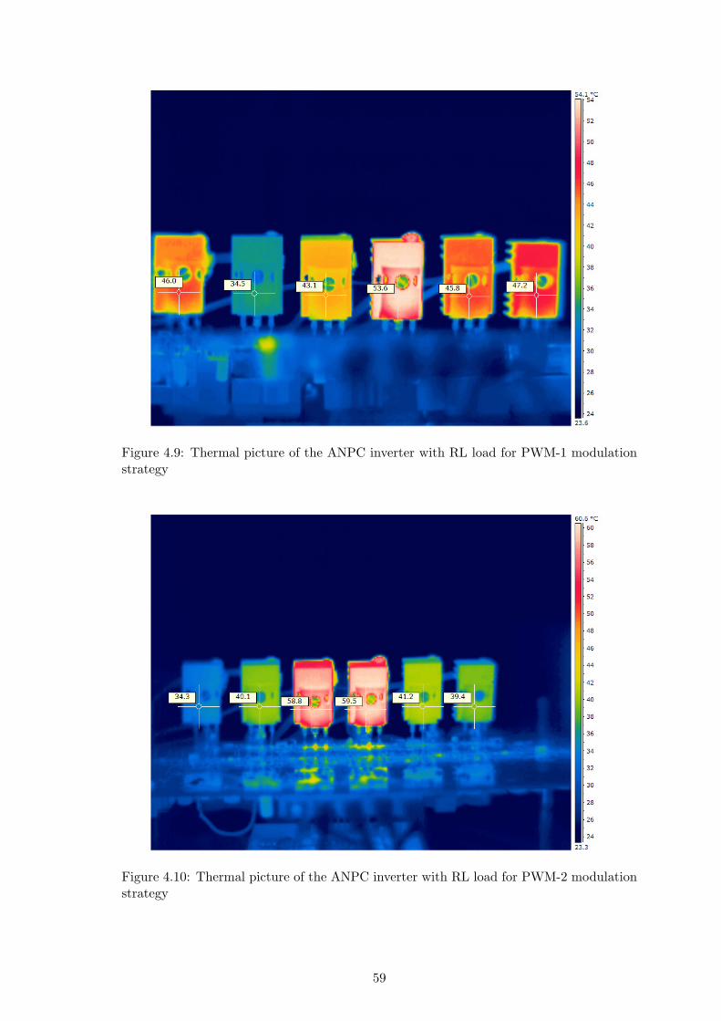
pwm-1-rl.jpg
Figure 4.9: Thermal picture of the ANPC inverter with RL load for PWM-1 modulationstrategy
pwm-2-rl.jpg
Figure 4.10: Thermal picture of the ANPC inverter with RL load for PWM-2 modulationstrategy
59

pwm-3-rl.jpg
Figure 4.11: Thermal picture of the ANPC inverter with RL load for PWM-3 modulationstrategy
pwm-df-rl.jpg
Figure 4.12: Thermal picture of the ANPC inverter with RL load for PWM-DF modulationstrategy
60

pwm-ald-rl.jpg
Figure 4.13: Thermal picture of the ANPC inverter with RL load for PWM-ALD modu-lation strategy
The measured temperatures of the switches which have been obtained for all the discussedmodulation strategies are summarized in Table 4.2.
Switch Modulation strategyPWM-1 PWM-2 PWM-3 PEM-DF PWM-ALD
S1 46 34,3 42,1 57,3 44,5S2 34,5 40,1 40,8 38,7 37,8S3 43,1 58,8 49,6 65,5 51,3S4 53,6 59,5 55,6 66,4 50,8S5 45,8 41,2 40,4 38,7 37,9S6 47,2 39,4 42,1 59 38,9
Table 4.2: The temperatures [oC] of the switching devices obtained for the RL load
Unlike the R load case, with RL load also the diodes will conduct. Because the diode isincorporated in the same case with the IGBT, the temperature measured with the thermalcamera represents the the sum of both the IGBT and diode power losses, manifested asheat.
With an RL load, the zero switches (S2 and S5) are expected to have more losses thencompared to the R load case, because they carry a higher current during zero state, dueto the stored energy in the inductance. The thermal pictures of the inverter for all themodulation strategies confirm this.
In order to explain the uneven temperature distribution amongst the complementaryswitches, a more thorough investigation in the laboratory would be needed. Based onthe the waveforms of the output voltages for PWM-1, PWM-2 and PWM-3 modulation
61

strategies1, which are presented in Figures 4.14, 4.15 and 4.16, it can be seen that theamplitude of the voltage during the negative cycle of the reference signal is higher thanthe amplitude during positive cycle of the reference signal. This unbalancing of the out-put voltage is also reflected in the temperature distribution amongst the switches. Theswitches which conduct during the negative cycle are hotter than the switches which con-duct on the positive cycle, so the switch S5 is hotter than S2 and the switch S4 is hotterthan S3.
0 0.01 0.02 0.03 0.04 0.05 0.06-250
-200
-150
-100
-50
0
50
100
150
200
250
Time [s]
Am
plitu
de [V
]
Figure 4.14: The waveform of the output voltage (measured on the resistor) for RL load(PF =0,85) with PWM-1 modulation strategy
0 0.01 0.02 0.03 0.04 0.05 0.06-250
-200
-150
-100
-50
0
50
100
150
200
Time [s]
Am
plitu
de [V
]
Figure 4.15: The waveform of the output voltage (measured on the resistor) for RL load(PF =0,85) with PWM-2 modulation strategy
1The waveforms for the PWM-DF and PWM-ALD strategies are missing due to the limited amount oftime for access in the laboratory
62

0 0.01 0.02 0.03 0.04 0.05 0.06-250
-200
-150
-100
-50
0
50
100
150
200
250
Time [s]
Am
plitu
de [V
]
Figure 4.16: The waveform of the output voltage (measured on the resistor) for RL load(PF =0,85) with PWM-3 modulation strategy
4.4 Summary
This chapter treats the laboratory implementation part of this report.
In the beginning of the chapter, the laboratory setup is described. The inverter usedin the experimental tests was a low voltage single-phase ANPC inverter developed by[7]. The control of the inverter has been implemented on a TMS320F28335 eZdsp. Thecommunication between the DSP and the semiconductor switches is achieved through aninterface which is compatible with this DSP board. In order be able to drive the switcheswith six independent signals, an extension board for the control part of the inverter legwas developed. The code for the control strategies which have been implemented on theDSP was generated using Matlab Simulink.
All five modulation strategies which have been simulated in Chapter 3, have also beentested experimentally. With the help of a thermal camera, temperature measurements havebeen performed on the inverter. Because in the semiconductor devices of the inverter, boththe IGBT and the diode are incorporated in the same case, the temperatures measuredwith the thermal camera represent the the sum of the power losses for both devices,manifested as heat.
All the tests have been performed only for the inverter mode of operation of the ANPCconverter, for both R and an RL load (PF = 0,85).
In the case of the resistive load, the experimental results confirm the simulation resultsobtained in the previous chapter in what concerns the distribution of the power losses(expressed as temperatures) amongst the switches of the inverter. The temperatures [oC]of the switching devices obtained for the resistive load are summarized in Table 4.3 (onthe next page).
In the case of the RL load (PF = 0,85), the loss balancing is not as evident as for theresistive load, due to the fact that in this case also the anti-parallel diodes will conduct,and therefore their losses will add to the losses of the IGBTs.
63

Switch Modulation strategyPWM-1 PWM-2 PWM-3 PWM-DF PWM-ALD
S1 70,9 53,9 42,5 61,1 68,8S2 34,2 36,5 31,9 33,3 35,7S3 55,1 78,2 46,5 65,2 65,2S4 57,9 77,5 50,6 66,4 64,4S5 37,3 36,3 33,4 33,4 35,7S6 68,3 53,1 45 62,9 57,5
Table 4.3: The temperatures [oC] of the switching devices obtained for the R load
An uneven distribution of the temperatures amongst the complementary switches is ob-tained. The waveforms of the output voltages have been measured, and it can be seen thatthe amplitude during the negative cycle of the reference signal is higher than the ampli-tude during positive cycle of the reference signal. This unbalancing of the output voltageis also reflected in the temperature distribution amongst the switches. So, the switcheswhich conduct during the negative cycle are hotter than the switches which conduct onthe positive cycle.
64

Chapter 5
Conclusions
5.1 Review of the main tasks
The goal of this project was to investigate different modulation strategies for the ActiveNeutral Point Clamped (ANPC) topology, in order to achieve an even distribution of thepower losses amongst the switches of the converter. Due to the fact that the most stresseddevice will limit the current capability of the converter, power loss balancing is desired.This way, the transferred power and switching frequency of the converter can be increased,without having to increase the costs by replacing the switches with higher rated ones orbringing improvements to the cooling system.
After the background an motivation of this project have been briefly presented, the maingoals and limitations were established.
The main theoretical concepts which have been used throughout the entire report havebeen presented in the beginning of chapter 2. After a brief presentation of the typesof power losses which can occur in semiconductor devices, the three-level converter con-cept was introduced, as an improvement brought to the two-level structure. The ActiveNeutral Point Clamped (ANPC) topology was then described. Compared to the basicNeutral Point Clamped (NPC) converter, this strategy allow by the use of an adequatemodulation strategy, to achieve a more balanced distribution of the power losses betweenthe semiconductor devices on the converter, and therefore overcome the main drawbackof the NPC. Several modulation strategies used for controlling the ANPC converter werepresented, with focus on how the power losses are distributed amongst the switches. Thetwo classical modulation strategies (PWM-1 and PWM-2) do not take advantage of themultiple possibilities of the ANPC topology to obtain the zero state. By using these twomodulations, there will always be an uneven distribution of losses between the inner andouter switches of the converter. A new modulation strategy, called PWM-3 has beeninvestigated. This strategy represents a combination of the two classical methods. Theswitching sequences of PWM-3 are obtained by using for 50% of the reference signal’speriod, the switching sequences of PWM-1 strategy and for the other 50%, the switchingsequences of PWM-2 strategy. This way, the switching losses are redistributed amongstthe inner and outer switches, hence bringing an improvement to the loss balancing issue.Other two modulation strategies were presented, namely PWM-DF [12] and PWM-ALD[10]. These two strategies also bring improvements to the loss unbalancing issue, by usingmore and different switching sequences in order to achieve the zero state.
The third chapter contains the simulation part of the report. In the beginning of thechapter, the structure of the simulation models was described. The general system wasdivided into three main blocks: the plant, composed of the DC sources, the single-phase
65

ANPC converter and the load, the modulator block and the losses calculation block. Inorder to be able to calculate the power losses of the inverters’ switches, their thermalmodel was implemented using PLECS Thermal Toolbox. Because in the inverter from thelaboratory setup, the IGBTs and the anti-parallel diodes are mounted in the same case, thesame configuration of the semiconductor devices was used in the simulations. The lossesof the converter are presented as the power losses of the IGBT and anti-parallel diodesummed for each of the devices. In this way, the behaviour of the semiconductor switchesin the simulations is similar to the behaviour of the semiconductor switches which havebeen used in the laboratory tests (IRG4PC40FD). All the modulation strategies whichhave been presented in the previous chapter have been simulated for a 10 kW resistiveload, with a frequency of the carrier waves equal to 15 kHz (except the PWM-DF strategy,where the frequency of the carriers was set to 7,5 kHz), and a unity modulation index(except from PWM-ALD strategy, where two reference signals are used, one having M= 1, while the other has M = 0,9). From the simulation results it can be seen that asexpected, with PWM-1 and PWM-2, the main drawback of the NPC topology is notovercome by the ANPC, hence loss balancing amongst the switches of the inverter was notachieved. With PWM-3, PWM-DF and PWM-ALD it can be seen that the total powerlosses are evenly distributed between the switches. Due to the fact that in the laboratorytests, the maximum load which could be used with the available equipment was of 650 W,the simulations have been repeated for this new situation, for both R and and RL load(PF = 0,85), in order to check if for this low power level, the issue of loss balancing is stillvalid.
The fourth chapter presents the laboratory part of this report. In the beginning of thechapter, the laboratory setup was described. The code for the control strategies which havebeen implemented on the DSP was generated using Matlab Simulink. All five modulationstrategies which have been simulated in Chapter 3, have also been tested experimentally.With the help of a thermal camera, temperature measurements have been performed onthe inverter. Because in the semiconductor devices of the inverter, both the IGBT andthe diode are incorporated in the same case, the temperatures measured with the thermalcamera represent the the sum of the power losses for both devices, manifested as heat.All the tests have been performed only for the inverter mode of operation of the ANPCconverter, for both R and an RL load (PF = 0,85). In the case of the resistive load, theexperimental results confirm the simulation results obtained in the previous chapter inwhat concerns the distribution of the power losses (expressed as temperatures) amongstthe switches of the inverter. In the case of the RL load (PF = 0,85), the loss balancing isnot as evident as for the resistive load, due to the fact that in this case also the anti-paralleldiodes will conduct, and therefore their losses will add to the losses of the IGBTs. In thiscase, an unbalancing of the output voltages has been observed on the oscilloscope. Thisunsymmetry was also reflected in the temperature distribution amongst the switches.
The final chapter of the report contains the conclusions and ideas for future work.
5.2 Future work
Because the experimental results which have been obtained for the RL load are not soclear, it could be of interest to perform more tests for this type of load, in order to studyhow the power losses are distributed amongst the semiconductor device of the converterand to discover the source of the unbalanced output voltage.
Only power losses (total for the IGBT and anti-parallel diode) are provided by theimplemented simulations. This information is enough if the purpose of the analysis is to
66

study the way that the losses are distributed amongst the switches of the inverter for aresistive load. In order to perform a more thorough investigation, especially for RL loads,some improvements could be brought to the simulations, like:
• semiconductor switch modelled by separate IGBT and diode;
• evaluation of the temperature in the simulation.
In order to study better the advantages of PWM-ALD strategy, simulations and exper-iments could be performed for different Stress In/Stress Out ratios, and for loads withdifferent power factors.
Due to the fact that the converter which has been used for the laboratory test was notbuild for loss balancing analysis purposes, the switches which have been used have theIGBT and the anti-parallel diode mounted in the same case. In this case it is impossibleto analyse only the IGBT power losses, for example. By building a new converter leg,which has the IGBT and diode mounted separately could allow a more detailed analysisof the power distribution.
The ANPC converter is used for high power medium voltage drives for industry, andso it would be of interest to study the loss balancing modulation strategies on a machineload.
67


Bibliography
[1] T. Bruckner, S. Bernet, Loss Balancing in Three-Level Voltage Source Inverters Apply-ing Active NPC Switches, IEEE 32nd Annual Power Electronics Specialists Conference,2001, Volume 2, Pages 1135-1140;
[2] A. Nabel, I. Takahashi, H. Akagi, A New Neutral-Point-Clamped PWM Inverter, IEEETransactions on Industry Applications, September 1981, Volume IA-17, Issue 5, Pages518-523;
[3] T. Bruckner, S. Bernet, H. Guldner, The Active NPC Converter and Its Loss-BalancingControl, IEEE Transactions on Industrial Electronics, June 2005, Volume 52 , Issue 3,Pages 855-868;
[4] Graovac Dusan, Marco Purschel, IGBT Power losses Calculation Using the Data-SheetParameters, Infineon Automotive Power, Application Note v 1.1, January 2009;
[5] Bin Wu, High-Power Converters and AC Drives, John Wiley & Sons Inc., First Edition,2006, ISBN 13-978-0-471-73171-9;
[6] Muhammad H. Rashid, Power Electronics Handbook, Acadamic Press, First Edition,2001
[7] Maciej Swierczynski, Andrzej Adamczyk, Modulation of Three Level Inverter withCommon Mode Voltage Elimination and DC Link Balancing, Aalborg University, 2009;
[8] Hongyang Wu, Xiangning He, Inhrent Correlation Between Multilevel Carrier-BasedPWM and Space Space Vector PWM:Principle and Application, 4th IEEE InternationalConference on Power Electronics and Drive Systems, Proceedings, 22-25 October 2001,volume 1, pages 276 - 281, ISBN 0-7803-7233-6;
[9] B.P. McGrath, D.G. Holmes, A Comparison of Multicarrier PWM Strategies for Cas-caded and Neutral Point Clamped Multilevel Inverters, IEEE 31st Annual Power Elec-tronics Specialists Conference, 18-23 June 2000, Volume 2, Pages 674 - 679, ISBN0-7803-5692-6;
[10] Lin Ma, Tamas Kerekes, Remus Teodorescu, Xinmin Jin, Marco Liserre, Pedro Ro-driguez, The PWM Strategies of Grid-connected Distributed Generation Active NPCInverters, IEEE Energy Conversion Congress and Exposition, 20-24 September 2009,pages 920 - 927, ISBN 978-1-4244-2893-9;
[11] Ionut Trintis, Active Neutral Point Clamped Converter, Aalborg University, 2008;
[12] D. Floricau, E. Floricau, M. Dumitrescu, Natural Doubling of the Apparent SwitchingFrequency using Three-Level ANPC Converter, International School on NonsinusoidalCurrents and Compensation, 10-13 June 2008, pages 1-6, ISBN 978-1-4244-2129-9;
[13] eZdspTMF38335 Technical Reference;
69

[14] International Rectifier, Insulated Gate Bipolar Transistor with ultra fast soft recoverydiode IRG4PC40FD - Datasheet;
[15] HS Marston Aerospace,Heat Sinks for Electronics Cooling - Technical Info, Availablefrom http://www.hsmarston.co.uk/technical technical 01.htm [cited on 16 April 2010];
[16] PLECS User manual, Version 2.2, 2009;
70

Appendix A
Heat sink selection
A very important aspect in converter design is the selection of the cooling system forthe semiconductor devices. The most handy solution is to passively cool the switches bymounting them on a heat sink. The purpose of the heat sink is to dissipate the heatgenerated by Joule effect due to the current which passes through the devices, preventingthem from becoming too hot, which would lead to their destruction. In order to betterobserve the temperature of each switch, individual heat sinks are going to be mounted.
For choosing the heat sink, the total power losses of the semiconductor device need to becalculated. For this calculation, the inverter is considered to be controlled with the PWM-2 modulation strategy, which stresses the most the semiconductor devices, especially theinner switches. The switching frequency is 15 kHz and the load is a 3 kW R load (PF =1).
The losses in the semiconductor device are represented by conduction and switching lossesfor both the transistor and the antiparallel diode, as presented in Equation A.1.
Ploss = Pcond + Psw [W ] (A.1)
The conduction losses can be calculated from Equation A.2 [4].
Pcond = VCE0 · ICav + rC · I2Crms
[W ] (A.2)
where Vf is the forward voltage drop at zero current [V], Iavg is the average current throughthe device [A], rf is the forward resistance [Ω] and Irms is the rms value of the currentthrough the device [A].
The forward voltage drop Vf and the forward transconductance are provided in thedatasheet of the selected semiconductor device (IRG4PC40FD) [14]:
VCE0 = 0, 9 V
gC = 9, 2 S
The forward resistance can be calculated from the transconductance as:
rC =1gC
= 0, 11 Ω
The switching losses can be calculated from Equation A.3 [4]:
Psw =1Tfsw
∫ Tsw
0e(i)dt [W] (A.3)
71

where fsw is the switching frequency [Hz], T is fundamental voltage period [s], Tsw is theswitching period [s], e(i) is the total switching energy losses for the IGBT together withthe reverse recovery diode [J].
In the IRG4PC40FD datasheet [14] it is provided a chart for the total switching lossesversus the collector-to-emitter current, for currents above 13 A. Due to the fact that inthe considered operating conditions, the current through the device is approximately 4 A,the given graph has been extended, as presented in Figure A.1.
y = 0,181x + 0,11R² = 0,9997
0
0,5
1
1,5
2
2,5
3
3,5
4
4,5
5
0 5 10 15 20 25 30
Total switching en
ergy losses [m
J]
Collector‐to‐emitter current [A]
Figure A.1: Typical switching losses versus the collector-to-emitter current
In order to analytically calculate the power losses, a Matlab Simulink simulation modelhas been developed (see Figure A.4 and Figure A.5). This way, the calculation can also beperformed also for other operating conditions of the inverter (different load, modulationtechnique, switching frequency, etc.)
The values of the total inverter losses for each semiconductor device are given in TableA.1.
Switch S1 S2 S3 S4 S5 S6
Total power losses [W ] 6,1 0 25 25 0 6,1
Table A.1: Total power losses of the semiconductor devices
As it can be seen from Table A.1, with PWM-2 modulation strategy the inner switches(S3 and S4) are the most stressed. The losses in these devices will be considered for sizingthe heat sink.
In order to size the heat sink the equivalent electrical model of thermal behaviour for theselected switch is considered (see Figures A.2 and A.3 on the next page) [15]. The otherheat sinks are going to be selected to be identical.
72

Figure A.2: Device and heat sink physical model
Tj Tc Th Ta
P
RhaRchRjc
Figure A.3: Equivalent electrical model for a semiconductor device, where: Q - heat sourcewhich has a current source as an electrical correspondent [W]; Tj - junction temperature[oC]; Tc - temperature of the case [oC]; Th - temperature of the heat sink [oC]; Ta -ambient temperature [oC]; Rjc - junction-to-case resistance [oC/W ]; Rch - case-to-heatsink resistance [oC/W ]; Rha is heat sink-to-ambient resistance [oC/W ]
In the equivalent electrical model, the temperatures are seen as node potentials. Thetemperature difference between the nodes is treated as a voltage drop on the equivalentthermal impedance, due to the carried losses [15]. The aim of the calculations is to assessthe maximum junction temperature of the semiconductor.
The model and the resulting equations are approximate, mainly because [15]:
• the heat transfer process is static or slowly varying over time (order of magnitude ofseconds);
• the calculations do not take into account that there are other paths of heat (betweenthe device and the ambient), which should be represented in the scheme by additionalresistances, but can be neglected in a first approximation;
• the event of heat transfer (especially between the heat sink and the ambient) isnonlinear because it involves simultaneously heat transfer by conduction, convectionand radiation;
• the presence of any other heat source nearby (like other sinks, power resistors, etc.)reduces the cooling efficiency;
• it is a model that has been simplified to one-dimension.
73

The junction-to-case resistance Rjc and the case-to-heat sink resistance Rch are given inthe datasheet of the semiconductor device IRG4PC40FD [14]:
Rjc = 0, 77 oC/W
Rch = 0, 24 oC/W
The maximum working temperature of the junction is Tj = 150 oC and the ambienttemperature is considered Ta = 25 oC. The heat sink-to-ambient resistance, Rha can beevaluated using Equation A.4 [15].
Tjmax − Ta = P · (Rjc +Rch +Rha) [oC] (A.4)
The required minimum thermal resistance for the heat sink can be determined from Equa-tion A.5 [15].
Rha =Tjmax − Ta
P− (Rjc +Rch) [oC/W ] (A.5)
The value which is obtained for the thermal resistance of the heat sink is Rha = 5 oC/W
74

Tota
l_Lo
sses
S6
0.00
55
Tota
l_Lo
sses
S5
6.15
8
Tota
l_Lo
sses
S4
25.0
3
Tota
l_Lo
sses
S3
25.0
2
Tota
l_Lo
sses
S2
0.00
55
Tota
l_Lo
sses
S1
6.15
7
Sw
it_Lo
sses
S6
0.00
55
Sw
it_Lo
sses
S5
0.06
312
Sw
it_Lo
sses
S4
18.9
4
Sw
it_Lo
sses
S3
18.9
3
Sw
it_Lo
sses
S2
0.00
55
Sw
it_Lo
sses
S1
0.06
31
Is1
Is2
Is3
Is4
Is5
Is6
PcS
1
PcS
2
PcS
3
PcS
4
PcS
5
PcS
6
PsS
1
PsS
2
PsS
3
PsS
4
PsS
5
PsS
6
Rth
[°C
/W]
4.99
5
PsS
3
PsS
2
PsS
1
PcS
6
PcS
5
PcS
4
PcS
3
PcS
2
PsS
5
PsS
6
PsS
4
PcS
1
PsS
1
PsS
2
PcS
2
Is6
Is5
Is4
Is3
PsS
3
Is2
PcS
3
PsS
6
PcS
6
PsS
5
PcS
5
PsS
4
PcS
1
PcS
4
PsS
3
PcS
3
Is1
Tj Ta
Rth
jc
Rth
cs
Con
d_Lo
sses
S6
0
Con
d_Lo
sses
S5
6.09
5
Con
d_Lo
sses
S4
6.09
5
Con
d_Lo
sses
S3
6.09
4
Con
d_Lo
sses
S2
0
Con
d_Lo
sses
S1
6.09
4
Figure A.4: Matlab Simulink simulation model for heat sink calculation

PsS612
PsS511
PsS410
PsS39
PsS28
PsS17
PcS66
PcS55
PcS44
PcS33
PcS22
PcS11
signal rms
In Mean
sqrt
Imean efcn
fref
f_switching
Uce0
1/gfe
0
0.001
Is66
Is55
Is44
Is33
Is22
Is11
Figure A.5: Matlab Simulink simulation model for heat sink calculation - subsystem
76

Appendix B
Extension interface board
The ANPC converter [7] was build to be driven with three optical signals, while the remain-ing three complementary signals were generated hardware by using a dead time generator.This feature became a limitation in some situations, like in the case of PWM-DF andPWM-ALD modulation strategies, where the switches needed to be controlled individu-ally, therefore requiring six independent switching signals. To overcome this limitation,another three opto receivers have been added. In order not to perform any hardwaremodifications on the inverter leg, an extension board containing the extra opto receivershas been built, and all the drive signals are routed to it, and then re-routed to the inverterleg through the pins where the dead time generator was.
The diagram and the PCB layout o the extension board can be seen in Figure B.1.
5
5
4
4
3
3
2
2
1
1
D D
C C
B B
A A
R
ENAR
S
ENAS
T
ENAT
OUTPUT ENA
RESET
GND
UU
UL
NU
NL
BU
BL
VCC
RST
ENARENASENAT
RESETOUTPUT ENA
OSC
RC IN
RC IN
OSC
UU
NU
BU
VCC
VCC
VCC
VCC
VCC
VCC
ENARENASENAT
RESETOUTPUT ENA
UL
NL
BL
Title
Size Document Number Rev
Date: Sheet of
PED2-840, Spring 2010
1.1
Extension interface for A/NPC
A
1 1Friday, May 21, 2010
Title
Size Document Number Rev
Date: Sheet of
PED2-840, Spring 2010
1.1
Extension interface for A/NPC
A
1 1Friday, May 21, 2010
Title
Size Document Number Rev
Date: Sheet of
PED2-840, Spring 2010
1.1
Extension interface for A/NPC
A
1 1Friday, May 21, 2010
R24.12kR24.12k
C3100nC3100n
C1100nC1100n
J1
CON6A
J1
CON6A
1 23 45 6
C5100nC5100n
C6100uC6100u
U5
IXDP630
U5
IXDP630
R1S3T5
OUTEN7 RST8
GN
D9
RCIN10
OSCOUT 11
TL 12TU 13
SL 14SU 15
RL 16RU 17
VC
C18
ENAR2ENAS4ENAT6
C7100nC7100n
C10100pC10100p
R37.32kR37.32k
U4con18
U4con18
11
22
33
44
55
66
77
88
99
18 18
17 17
16 16
15 15
14 14
13 13
12 12
11 11
10 10
U6
IXDP630
U6
IXDP630
R1S3T5
OUTEN7 RST8
GN
D9
RCIN10
OSCOUT 11
TL 12TU 13
SL 14SU 15
RL 16RU 17
VC
C18
ENAR2ENAS4ENAT6
U2
HFBR 2521z
U2
HFBR 2521z
Vo 1GND 2VCC 3RL 4NC5
NC8
J2
CON6A
J2
CON6A
1 23 45 6
C8100nC8100n
C2100nC2100n
U9
74HC04
U9
74HC04
1A1 1Y 22A3
2Y 43A53Y6
GN
D7
4Y8 4A95Y 105A 11
6Y 126A 13VC
C14
C4100uC4100u
U1
HFBR 2521z
U1
HFBR 2521z
Vo 1GND 2VCC 3RL 4NC5
NC8
U3
HFBR 2521z
U3
HFBR 2521z
Vo 1GND 2VCC 3RL 4NC5
NC8
R415kR415k
R14.12kR14.12k
Figure B.1: The circuit diagram of the extension interface board
77

Figure B.2: The PCB layout of the extension interface board
78

Appendix C
List of used laboratoryinstruments
The instruments which have been used for the laboratory test setup are given in TableC.1.
Instrument Type AAU inventory code
300 V, 5 A DC Power Supply Delta Elektronika GPL - PERES24 V, 3 A DC Power Supply GW-INSTEK GPS-4303 4 79059
56061Load Resistor ASEA Education AB-5514 152-B 29511Load Inductor ASEA Education 29512
Single-Phase Power Analyser Voltech PM 100 35596
Table C.1: Laboratory instruments
79


Appendix D
Contents of the enclosed CD
The enclosed CD contains:
• Report - this folder contains the the report in PDF format
• References - this folder contains the articles used as reference in the report, whenavailable in electronic format
• Simulations - this folder contains the simulation files
• Laboratory implementation - this folder contains the Simulink models used for gen-erating the code for DSP implementation, the Code Composer projects and thethermal pictures of the inverter
81