this document has been reproduced from … · -overhead stream as the feed to cvd reactor ......
TRANSCRIPT

N O T I C E
THIS DOCUMENT HAS BEEN REPRODUCED FROM MICROFICHE. ALTHOUGH IT IS RECOGNIZED THAT
CERTAIN PORTIONS ARE ILLEGIBLE, IT IS BEING RELEASED IN THE INTEREST OF MAKING AVAILABLE AS MUCH
INFORMATION AS POSSIBLE
https://ntrs.nasa.gov/search.jsp?R=19810021975 2018-05-27T10:49:32+00:00Z

76 - 7DOE/JPL - 956045 -61/1
DISTRIBUTION CATEjOR: UC-63
(NACA - -r. -16»773) SILICON rflUDUC1 IGN s81-30517
EVALUATIONS QuurteL ly TeCt,l.lc: it eK04UassFe Fort, 18 May - J1 Jul. 1 y 01 Gk xasFeseaLch atui rnylt,tt'rit:y .116t. nC.) N ULC1dS
NC A02/MF A01 k JCL 1UA -7196
SILICON PRODUCTION PROCESS EVALUATIONS
QUARTERLY TECHNICAL PROGRESS REPORT (I)
Issue Date: August, 1981
Reporting Period: May 18 - July 31, 1981
TREITeas Research and Engineering Institute, Inc.
6116 WASHINGTON
GROVES, TEXAS 77619
JPL Contract No. 956045
Contractural Acknowledgement
The JPL Low-Cost Solar Array Project is sponsored b y the U.S. Department
of Energy and forms part of the Solar Photovoltaic Cunverbion Program toinitiate a major effort toward the development of low-colt solar arrays.This work was performed for the Jet Propulsion Laboratory, CaliforniaInstitute of Technology by agreement between NASA and DOE.

DISCLAIMER
"This report was prepared as an account of work sponsored by the
United States Government. Neither the United States nor the UnitedStates Department of Energy, nor any of their employees, nor any oftheir contractors, subcontractors, or their employees, makes anywarranty, express or implied, or assumes any legal liability or
responsibility for the accuracy, completeness or usefulness of anyinformation, apparatus, product or process disclo. :ed, or representsthat its use would not infringe privately owned rights."
f^

ABSTRACT
During this reporting period, chemical engineering analysis of theHSC process (Hemlock Semiconductor Corporation) for producing siliconfrom dichlorosilani was initiated.
For the preliminary process design, Hemlock SemiconductorCorporation was contacted in regard to providing a process flowsheetwhich best represents the HSC process at this point in time and which
should be used for the chemical engineering analysis of a 1,000 MT/yrplant for solar cell grade silicon.
Major efforts in the chemical engineering analysis of the HSCprocess were devoted to the preliminary process design of a plant toproduce 1,000 MT/yr of silicon using the technology. Progress andstatus for the plant design are reported for the primary activities
of base case conditions (60X), reaction chemistry (50X), process flow
diagram (35X), energy balance (107.), property data (10X), andequipment design (Sx).

TABLE OF CONTENTS
PAGE
I. CHEMICAL ENGINEERING ANALYSIS .................. 1
II. SUMMARY — CONCLUSIONS .......................... 9
III. PLANS .......................................... 10
MILESTONE CHART
'a

I. CHEMICAL ENGINEERING ANALYSIS
Chemical engineering analysis of the HSC process WemlockSemiconductor Corporation) for silicon was initiated during thisreporting period.
In performing the chemical engineering analysis, a process flowsheetis required for the preliminary process design. Hemlock SemiconductorCorporation has been contacted in regard to providing a process flowsheetwhich best represents the HSC process at this point in time and which shouldbe used for the chemical engineering analysis of a 1,000 MT/yr plant forsolar cell grade silicon.
The HSC process is based on the chemical vapor deposition ofdichlorosilane (DCS) with hydrogen to produce polysilicon. This DCSdeposition reaction rate is fast and has the following representativechemical reacti -S. ;quation:
SiH2C12 + H2 -+ Si + + By-products
The above reaction equation may include several reaction steps.Chemical equilibrium is involved and in reality, several chlorosilanes(such as SiH2C1 21 SiHC13 and SiC14 ) are also present in the gas phaseby-products.
For chemical engineering analysis of the HSC process, progress andstatus are summarized below for primary activities:
Prior Current
1. Base Case Conditions 0% 60%
2. Reaction Chemistry 0% 50%
3. Process Flow Diagram 0% 35%
4. Material Balance 0% 35%
5. Energy Balance OX 10%
6. Property Data 0% 10%
7. Equipment Design 0% 5%
The detailed status sheet for the chemical engineering analysis isshown in Table I-1 for the preliminary process desigii of the plant. Thebase case conditions (issue 1) and reaction chemistry are given inTables I-2 and I-3.
1

The process flow diagram (issue 1) is presented in Figure I-1.The conceptual-type process flowsheet in the figure shows the major unitoperations involved in the production of the silicon product. Theflowsheet, as shown, was prepared primarily from the 4th and 5thquarterly technical reports of Hemlock Semiconductor Corporation. Withinthis regard, Hemlock Semiconductor Corporation has been contacted againto provide an updated process flowsheet which best represents the HSCprot.ess at this point in time and which includes any process changes basedon development work completed since the earlier quarterly technical reports.
2

d
H
NNW
U a
ua
m o^
u>
^i ~
^a
t7 NNN
mC UC a^
s^ m w a c>
H
u-.4a
^^•^ u10M+ .+ u4 x a u
a40a uu a ^uvaa", w °•.' u
y^
Iy •.r c ^cauC y
u woa ;
a4a ^ w '5 ma ^> I es^^ m bS'^
.+aa.4 u .^
awatu^► ^a^aea u
S. . °wa N rIN^'"► .-1N a •.1N ^'+a} ^rlNf'1CC .t^7r+ry r+
3
z
NaNa
u
11.4
O u
L t
M
2 00000 Coco 00000 coo 0co.
4 some seeyN
yS
a
'9 t
so m 4.1 a o
>wa^p og so III ^ wa
0.4w
t 4F
.+ A+
a -4N A ;1r;(4 4
co
I0
.. to
wvp^0co
•0 120 P4 w
f3 b w
1 1
q°J1 1
^pu w
F ^+ O '0 ate► O 'O
ova ,0aa
^o1w .1 n 4 a ri CM* w
a
g1M .^1dap,
a «c+ uo0•
oesea ease 0000 0000
Ad
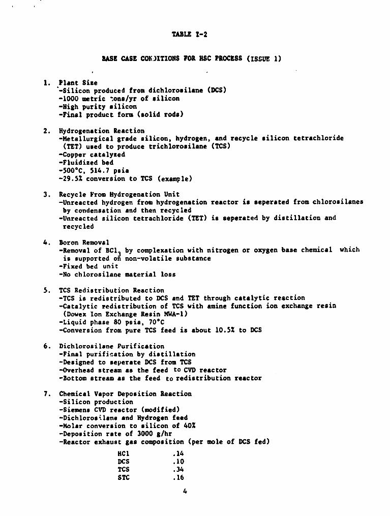
TABLE 1-2
BASE CASE COIF:)ITIONS FOR HSC PROCESS (ISSUE 1)
1. Plant SizeSilicon produced from dichlorosilane (DCS)
-1000 metric tons/yr of silicon-High purity silicon-Final product form (solid rods)
2. Hydrogenation Reaction-Metallurgical grade silicon, hydrogen, and recycle silicon tetrachloride(TET) used to produce trichlorosilane (TCS)
-Copper catalyzed-Fluidized bed-500°C, 514.7 psia-29.5% conversion to TCS (example)
3. Recycle From Hydrogenation Unit-Unreacted hydrogen from hydrogenation reactor is seperated from chlorosilanesby condensation and then recycled
-Unreacted silicon tetrachloride (TET) is seperated by distillation andrecycled
4. Boron Removal-Removal of BC1 3 by complexation with nitrogen or oxygen base chemical whichis supported on non-volatile substance
-Fixed bed unit-No chlorosilane material loss
S. TCS Redistribution Reaction-TCS is redistributed to DCS and TET through catalytic reaction-Catalytic redistribution of TCS with amine function ion exchange resin(Dowex Ion Exchange Resin MWA-1)
-Liquid phase 80 psi&, 70°C-Conversion from pure TCS feed is about 10.5% to DCS
6. Dichlorosilane Purification-Final purification by distillation-Designed to seperate DCS from TCS-Overhead stream as the feed to CVD reactor-Bottom stream as the feed to redistribution reactor
7. Chemical Vapor Deposition Reaction-Silicon production-Siemens CVD reactor (modified)-Dichlorosilane and Hydrogen feed-Molar conversion to silicon of 40%-Deposition rate of 3000 g/hr-Reactor exhaust gas composition (per mole of DCS fed)
HC1 .14DCS .10TCS .34STC .16
4

TABLE I-2 (CONTINUED)
8. Recycle From MID Reactor-Chlororilanes are recovered from a refrigeration process-Hydrogen is seperated from HC1 by adsorption process and recycledback to the CVD reactor
-Hydrogen chloride (HC1) is recovered as a salable by-product
9. 'Slim Rod Pullers-Prepare slim rods (small filaments)-Slim rods used in Siemen's CVD reactor for silicon deposition-Slim rod diameter of 6mm (approx. k inch)
10. Operating Ratio-Approximately 85% utilisation (on stream time)-Approximately 7445 hour/year production
11. Storage Consideration-Feed materials (several week supply, approx. 1 month)-Product (two shifts storage)-Process (several hours to 1 shift)
12. Waste$ Treatment-Scrub and neutralize waste gas streams-Caustic solution used to neutralize
5
—

TABLE 1-3
REACTIOI4 CHEMISTRY FOR HSC PROCESS
. 1. &drochlorinatian Reaction
3SiC14 + Si + 2H2 f 4SiHC13
2. Redistribution Reaction
2SihC13 f SiH2C12 + SiC14
3. Waste Treatment (rep resent at i ve - overate
SiH2Cif) + Ca(OH)2 !"Si02 + CaCl 2 + 2H20
SiHC1 3 + 1.5Ca(OH) 2 U.0. Si02 + 1.5CaC12 + 2H20
SiCl 4 + 2Ca(OI1) 2 ammo, Si02 + 2CaC1 2 2H2O
4. Decomposition Reaction
SiH2C12 + H2 -' Si + By-Products
Note:
1. Reaction 1 product contains H2 , HC1, SiCl4 , SLW13 , SiH2C12 (trace),other trace chlorides
2. Reaction 2 product contains SiHC1 3 ,Sicl4 , SiH2C12 , S'R3C1
3. By-products in reaction 4 include H2 , HU, SiH2C12 , SiHC13and SiC14

O
a. ^CY
NOIlISOd_IIJI I kHAA0:):-IHNO, I"I1S INIA
NO I LV-- I HOARJNI I.V1. 11 (INV
NO SS3MM0
'= NOI.I.t''1 .11.1 S 111
\^^Ilt'SN3t]N0:1
^_ r NO I .0 V 3 H
\u1111fll HIS I(I'M -- ^r
t
Q No I .I t i l l .l.'i l ( i^II.VN1801R)OM(I. lI
•^ st-
AIX1h
OjG `
E
vvvvu0
L:N
0w
utv.3OwvuuO
i
ui+
7

II. SUWAAY - CONCLUSIONS
The following summary-conclusions are made as a result of achieve-ments during this reporting period.
1. Chemical engineering analysis of the HSC process (Hemlock SemiconductorCorporation) for silicon was initiated.
2. Hemlock Semiconductor Corporation has been contacted in regards toproviding a process flowsheet which should be used for the chemicalengineering analysis of a 1,000 MT/yr silicon plant.
3. For chemical engineering analysis of the HSC process, major effortswere devoted to the preliminary process design of a plant :o produce1,000 NT/yr of silicon using the technology.
4. Progress and status hre reported for the primary design activities ofbase case conditions (602), reaction chemistry (50X), process flowdiagram (35%), material balance (35X), energy balance (10x), propertydata (10X) and equipment design 0%).
9

. 9
III. PLANS
Plans for the next reporting period are sus rised below:
1. Continue chemical engineering analysis of the HSC process(Hemlock Semiconductor Corporation) for silicon.
2. For the preliminary process design, major efforts will bedevoted to:
- base case conditions
- reaction chemistry
- process flow diagram
- material balance
- energy balance
- equipment design
10

l s
NGo
w I '
Ii
-^
^
"7
I ^
I
i
OI
z
O I
' I
¢
I I i• I I i
^I^
V,O
S
O1
OzF••vaF-zcU
JL1.^y
H
vwzFN{s7JE
trzGF-
7:c
FUCca
zcU
J
IIu
V1 G1 6:
G u^ •J L C v> c E v u m c
-+ d 3 -' = u of G
Q d L c9 IL 7 a* 4]V7 C ^' L^ T D Q• d
^ O to e0 u W a '^CV a1 w w a/ C.I. w w wu^ w u u a, w CL
7 0 0 3
Vf ^ O ++ a, O • ^+ ^ w
E ^ cr a E W G.. w E .^ warU 'I Cc v, O
y• O
C ^ In U
In • •+ G ^n u u u Hv U O m P c, U. m tr
• 41 U O ^O ++ w O G13 A a U 7 0 > U G.C m v O C w1Q N cfl u >, W U ^••^ u a
v, U r u rJV ar = .- w L u O
• u d —+ O G c •u QE o w 3 ^+ O 2O w m R u n c9 1+c a cc x ^ ^ ,.^ a. c.. c..0u
W .• N c'1 J LY+ p n oG
• "••• ^^ 3dA• .91 1 C WbOi 7NINNVIA IV;b3AINn