theory of dielectric nanofilms in strong ultrafast optical...
TRANSCRIPT

PHYSICAL REVIEW B 86, 165118 (2012)
Theory of dielectric nanofilms in strong ultrafast optical fields
Vadym Apalkov and Mark I. StockmanDepartment of Physics and Astronomy, Georgia State University, Atlanta, Georgia 30303, USA
(Received 17 July 2012; revised manuscript received 26 September 2012; published 11 October 2012)
We theoretically predict that a dielectric nanofilm subjected to a normally incident strong but ultrashort (afew optical oscillations) laser pulse exhibits deeply nonlinear (nonperturbative) optical responses which areessentially reversible and driven by the instantaneous optical field. Among them is a high optical polarization anda significant population of the conduction band, which develop at the peak of the pulse and almost disappear afterits end. There is also a correspondingly large increase of the pulse reflectivity. These phenomena are related toWannier-Stark localization and anticrossings between the Wannier-Stark ladders originating from the valence andconduction bands leading to optical “softening” of the dielectric. Theory is developed by solving self-consistentlythe Maxwell equations and the time-dependent Schrodinger equation. The results point out to a fundamentalpossibility of optical-field effect devices with the bandwidth on the order of optical frequency.
DOI: 10.1103/PhysRevB.86.165118 PACS number(s): 72.20.Ht, 42.65.Re, 77.22.Jp
I. INTRODUCTION
Experimental availability of intense ultrashort (a fewfemtosecond-long) optical pulses with just a few oscillationsof optical field opens up unique possibilities of optical controlof the electric and optical properties of dielectric materialswithin femtosecond time scale.1,2 The electric field in suchintense optical pulses is comparable to the internal fieldsacting on valence electrons in atoms and solids and is on theorder of a few V/A.2,3 Interaction of the electrons of a solidwith such strong fields has long been the subject of intensiveresearch.4–8 A strong-field optical pulse induces deep changesof the system, which can be reversible for a short enoughpulse.3,9–13
For semiconductors and their heterostructures, the opticalfield causes decrease of the bandgap between the valenceand conduction band known as Franz-Keldysh effect14,15 andquantum-confined Stark effect,16,17 respectively. For conju-gated molecules, which are organic semiconductors, it hasbeen predicted that the Stark effect decreases the gap betweenthe occupied and unoccupied molecular orbits leading toabsorption of the initially non-resonant pulses and electricalcurrents due to the ω − 2ω interference.18
A dielectric subjected to a weak optical field reacts to itschange instantly (adiabatically) as long as the laser frequencyω0 is small enough, ω0 � �g/h, where �g is the gap betweenthe valence band (VB) and conduction band (CB); e.g, forsilica �g ≈ 9 eV. This adiabaticity implies that the light-matterinteraction is fully reversible: after the pulse end, the systemreturns to its ground state, the residual excited-band populationis small, and so is the residual interband polarization. This isexpected for wide-bandgap dielectrics.
When the pulse field F increases, approaching the criticalfield strength Fcrit, which induces a change in electron potentialenergy by �g over the lattice period a ∼ 5 A, the adiabaticband gap decreases and completely collapses, where
Fcrit = �g
|e|a ∼ 2V
A, (1)
and e is electron charge.Previously, theoretical analysis of interaction of a intense
optical pulse with dielectric media was mainly restricted
to relatively long pulses with duration �100 fs. For suchpulses, the electron dynamics in the time-dependent fieldof the pulse be described in terms of the density matrixwhose evolution is determined by rate equations with phe-nomenological relaxation and generation times.19–23 In thisdescription, the effect of the pulse electric field is restrictedto generation of an electron-hole plasma through multiphotonor collisional ionization processes. Such rates as functions ofthe instantaneous electric field are usually introduced into themodel phenomenologically.
Another theoretical approach to interaction of ultrashortoptical pulse with semiconductor and dielectric media wasintroduced in Refs. 24–26. In these publications, a coupledsystem of Maxwell equations and time-dependent density-functional theory equations is solved numerically for diamondor silicon. In Ref. 26, the frequency of the pulse is close tothe interband gap, i.e., the system is close to the resonanceconditions. Therefore, although the duration of the pulse issmall, ∼10 fs, the dielectric system experiences a nonadiabaticdynamics with high residual excitation and a strong increaseof the pulse reflectance.
In the present article, we consider an extremely intense andultrashort pulse with duration of a several femtoseconds, andthe dielectric system far away from the resonant conditions.Specifically, we consider silica with bandgap �g ≈ 9 eV andpulse carrier frequency hω0 = 1.5 eV. With relaxation time∼20 fs, the electron dynamics for such an ultrashort pulseis expected to be field-driven and coherent (Hamiltonian),which can be described in terms of wave functions.11,13 Weintroduce a coupled system of Maxwell equations and the time-dependent Schrodinger equation, and solve it numerically. TheHamiltonian of the dielectric system is of the nearest neighbortight-binding type with the parameters chosen to reproduce theband structure of silica. Within this approach, the electric fieldof the pulse couples the states of the VB and the CB of thedielectric. Inherent in this system, electrons are dynamicallytransferred to the CB without any assumptions about thegeneration rate. We apply this approach to a nanofilm of silicawith a thickness of �150 nm.
Under such conditions, the underlying electronic dynamicsis characterized by a strong localization of the Wannier-Stark(WS) states.7,27 These states originating from a given band
165118-11098-0121/2012/86(16)/165118(13) ©2012 American Physical Society

VADYM APALKOV AND MARK I. STOCKMAN PHYSICAL REVIEW B 86, 165118 (2012)
are separated by the Bloch oscillation frequency,28 whichsignificantly exceeds ω0. Thus the electron dynamics is mostlyadiabatic except for anticrossings of the Wannier-Stark levelsoriginating from different bands. At those anticrossings, richdynamics appears, which generally is a superposition of bothdiabatic and adiabatic processes. This leads to “softening”of the system: enhanced optical responses of the dielectric,in particular strong polarization and reflection of the pulse,which are deeply nonlinear (nonperturbative) phenomena. Forthe strong ultrafast fields that are still below the threshold of thedielectric breakdown, the dynamics is reversible: the electronpopulation of the CB left after the pulse end is very low incontrast to a relatively high CB population during the pulse.
With respect to the previous prediction of the adiabatic met-allization of dielectric nanofilms,11,13 a significant differenceis that the present processes are too fast to be predominantlyadiabatic. Also of fundamental importance is that in the presentwork the pulse field is parallel to the surface while in Refs. 11and 13 it is normal to the surface causing appearance of theso-called quantum bouncer states playing an important role.
The paper is organized as the following. In Sec. II, wederive the main system of equations, which includes theMaxwell equations and the Schrodinger equation. In Sec. III,we introduce the Wannier-Stark states of CB and VB, andcoupled adiabatic states of electron system in the externalelectric field. We discuss formation of the Wannier-Starkstates of a single band for time-dependent electric field of theexcitation near-infrared (NIR) pulse. In Sec. IV, we present theresults of the calculations and discuss physical interpretationof these results. In Sec. V we present the concluding discussionof the obtained results.
II. MODEL AND MAIN EQUATIONS
A. Propagation of optical pulse
We study propagation of an optical pulse using a coupledsystem of equations, consisting of Maxwell equations, whichdescribe the propagation of the pulse in a system with a knownpolarization, and the Schrodinger equations, which determineelectron dynamics and the polarization of the electron system.The Maxwell equations are written down in the followingform:
∇ · D = 0, (2)
∇ · B = 0, (3)
∇ × F = −1
c
∂B∂t
, (4)
∇ × B = 1
c
∂F∂t
+ 4π
c
∂P∂t
, (5)
where B is magnetic field, F is electric field, and D = F + 4πPis the electric displacement field.
The polarization P of the dielectric medium is determinedby electron dynamics. This polarization, which is calculatedin the next section, depends on the electric field of the pulse ina strongly nonlinear manner due to strong mixing of CB andVB states in a high electric field.
Solution of the Maxwell equations determines the prop-agation of the optical laser pulse and the fields outside and
z0
dielectric film
FIG. 1. (Color online) Schematic illustration of the pulse nor-mally incident on the dielectric film. The pulse is propagating in thepositive direction of axis z. The dielectric film of a finite thickness,d < 150 nm, is placed at z = 0. The size of the system in z directionis 6000 nm.
inside the dielectric. The way we solve them takes intoaccount the boundary conditions at the surface of dielectricfilm automatically. We assume that the optical pulse propagatesalong the positive direction of the z axis, i.e., it is incidentnormally on the dielectric film. In this case, all variables inthe Maxwell equations depend on z only, and the problembecomes effectively one-dimensional.
We solve the Maxwell equations numerically by the finitedifference time domain (FDTD) method29,30 for a finite sizesystem with the absorbing boundary conditions. The size ofthe computational space in the z direction is 6000 nm withthe coordinates of the boundaries z1 = −3000 nm and z2 =3000 nm. The dielectric film is placed at the midplane ofthe system, i.e., it is centered at z = 0. The optical pulseis generated at the left boundary and propagates along thepositive direction of the z axis with the polarization of theelectric field along the x axis—see Fig. 1. We assume thatthe pulse has the following shape:
Fx(t) = F0e−(�vt)2
cos(ω0t), (6)
where F0 is the amplitude of the pulse, which is related to itspower, P , thorough the relation P = cF 2
0 /4π ; τp = 1/�v isthe duration of the pulse, ω0 is the carrier frequency of thepulse. Below we assume that the frequency of the pulse is inthe near-infrared (NIR) range, hω0 = 1.5 eV, and the durationof the pulse is τp = 4 fs.
In FDTD solutions of the Maxwell equations, we choosethe spatial step to be 1 nm, while the time step is 0.7 as (1 as =10−18 s). These values provide convergence for boththe Maxwell equations and the Schrodinger equation—seeSec. II B.
B. Electron dynamics
We capitalize on the fact that in our case the pulse lengthτp = 4 fs is very short. In fact, it is much shorter than typicaltime of the electron-electron Coulomb interaction τe. Forinstance, in such a good metal as silver, τe ≈ 20 fs—see,e.g., Ref. 31, i.e., τp � τe. Hence, during the pulse durationthe electron-electron collisions do not have time to produce asignificant effect on the electron dynamics. Correspondingly,we will neglect the Coulomb interaction and describe thelight-matter interaction by one-particle Schrodinger equation.
165118-2

THEORY OF DIELECTRIC NANOFILMS IN STRONG . . . PHYSICAL REVIEW B 86, 165118 (2012)
The electron dynamics in a periodic lattice potential in thepresence of an external electric field Fx is described by theHamiltonian:
H = p2
2m+ V (r) + eFx(z,t)x, (7)
where V (r) is the periodic crystal potential, m is the electronmass, and e is elementary charge. The electric field, Fx(z,t),which is calculated from the Maxwell equations (2)–(5),depends on the z coordinate and time t .
Without an external electric field, the periodic potential,V (r), produces the standard band structure of a solid withconduction and valence bands. The external electric fieldresults in time-dependent coupling between different bands.For Fx(z,t) periodic in t , which our field is not, such a couplingwould be described by quasienergies.
Below we carry out our analysis for a multiband systemthat includes both the conduction and valence bands. Wedenote the numbers of the conduction and valence bands asNc and Nv , respectively, where the total number of bandsis Nbands = Nc + Nv . The bands are labeled by index α =1, . . . ,Nbands.
For simplicity, we also assume that the periodic potential isseparable in the x,y, and z-directions. Then for each value ofthe z coordinate, the electron dynamics in the x direction, i.e.,in the direction of external electric field, becomes decoupledfrom the motion along the z and y directions. Correspondingly,in the y and z directions the potential is periodic with period a.In the x direction, the potential is aperiodic: it is a superpositionof the periodic crystal potential and the external potentialof the uniform electric field, eFx(z,t)x, depending on the z
coordinate as a parameter and on time t .In the absence of an external field, the eigenfunctions of
Hamiltonian (7) in the x direction are Bloch functions, ψαk(x),which are labeled by wave vector k, −π/a < k � π/a, andhave the following form:
ψαk(x) = 1
2πeikxuαk(x), (8)
where uαk(x + a) = uαk(z) are periodic Bloch unit-cell func-tions. In the zero external field, the Bloch functions diagonalizethe Hamiltonian (7) yielding energy dispersion relation Eα(k)for a band α.
We use an approximation of the tight-binding model32,33
for dispersion relations of the conduction and valence bands,
Eα(k) = εα + �α
2cos(ka), (9)
where �α is the width of band α and εα is the band offset,which is the midpoint of the band α.
The external electric field, Fx(z,t), introduces coupling ofstates of different bands and also causes time dependence ofthe electronic wave functions. Using the Bloch functions asthe basis, we can express the general solution of the time-dependent Schrodinger equation in the following form:
�(x,z,t) =Nbands∑α=1
√a
2π
∫ π/a
−π/a
dkφα(k,z,t)ψαk(x). (10)
Here the dependence of the wave function, �(x,z,t), on coor-dinate z is due to electromagnetic wave propagation expressed
as the dependence Fx(z,t) on coordinate z. Substitutingexpression (10) of the wave function into the Schrodingerequation ih∂�/∂t = H�, we obtain equations34,35 on expan-sion coefficients φα(k,z,t)
ihdφα(k,z,t)
dt=
[Eα(k) + ieFx(z,t)
d
dk
]φα(k,t)
+Fx(z,t)∑α′
Zαα′φα′(k,z,t), (11)
where
Zαα′ = e
a
∫ a
−a
dzuαk(z)∗i∂
∂kuα′k(z) (12)
are parameters of the model, which are the dipole matrixelements between the unit-cell Bloch functions of bands α
and α′.For a single band and in a constant electric field Fx ,
solutions of Eq. (11) are Wannier-Stark states,27,28 which areparametrized by an integer quantum number l and have wavefunctions35
φαl(k) = ei[lak+γα sin(ka)], (13)
where γα = �α/(2eaFx). In the coordinate representation,
φαl(x) = Jl−x/a(γα), (14)
where Jn(x) is the Bessel function of the first kind.The corresponding energies of the Wannier-Stark states are
εαl = εα + leaFx. (15)
These energies are equidistant and form the so-called Wannier-Stark ladder36–38 with the levels separated by the Bloch-oscillation frequency
ωB = eaFx/h. (16)
This spacing physically corresponds to the energy needed tomove an electron by one lattice constant in the field direction.Thus, in the constant (or, adiabatic) electric field, the electronspectrum of the system is universal: each band gives rise to aWannier-Stark ladder with the same level spacing hωB . Whilethe form of the Wannier-Stark wave functions (13) or (14)are specific for the tight-binding approximation, i.e., model-dependent, the energy spectrum of the Wannier-Stark statesdepends only on the lattice constant and is model-independent.
In a time-dependent electric field Fx(z,t), it is convenientto solve the Shrodinger equation (11) using an adiabaticbasis of the time-dependent eigenfunctions φαl(k,z,t) and thecorresponding eigenenergies εαl(z,t), which acquire their timedependence due to that of Fx(z,t). These adiabatic basis wavefunctions we chosen as
�αl(k,z,t) = exp
[− i
h
∫εαl(z,t)dt
]φαl(k,t,z), (17)
where we have explicitly indicated the evolutionary exponentdue to the phase accumulation of the adiabatic solution.
We emphasize that this adiabatic basis describes a systemof uncoupled Wannier-Stark ladders of different bands anddoes not take into account the coupling between them due tothe Zener tunneling.39 We will call it an uncoupled adiabaticbasis. It is different from the complete adiabatic basis, which
165118-3

VADYM APALKOV AND MARK I. STOCKMAN PHYSICAL REVIEW B 86, 165118 (2012)
is a solution of the full Scrodinger equation in a stationary(adiabatic) external field.
We perform a discreet Fourier transform of the adiabaticbasis wave functions (17) from the integer variable l to“quasimomentum” −π < q � π defined as
�αq(k,z,t) =∑
l
e−iql
√L
�αl(k,z,t). (18)
Then the solution of the Schrodinger equation (11) can beexpressed in the following form:
φα(k,z,t) =∑
q
βα(q,z,t)�αq(k,z,t), (19)
where βα are expansion coefficients, which satisfy the follow-ing system of equations:
dβα(q,z,t)
dt= iμα(t,z)βα(q,z,t)
− iFx(z,t)
h
∑α′
Zαα′καα′βα′ (q,z,t). (20)
Here
μα(z,t) = −dγα
dtsin
(q + ea
h
∫Fx(z,t)dt
)(21)
and
καα′ = exp
{i
[tεα − εα′
h
+ (γα′ − γα) sin
(q + ea
h
∫Fx(z,t)dt
)]}, (22)
where, as everywhere else in this article, α,α′ = 1, . . . ,Nbands.Eliminating the diagonal terms from the system (20) via the
following substitution:
βα(q,z,t) = βα(q,z,t)ei∫
μαdt , (23)
we obtain the final system of equations, which describescoupling of the states of the conduction and the valence bands,
dβα(q,z,t)
dt= −i
Fx(z,t)
h
∑α′ =α
Qαα′ (q,z,t)βα′ (q,z,t), (24)
where we have denoted
Qαα′(q,z,t) = Zαα′ exp
{i
[tεα − εα′
h+ �α − �α′
2h
×∫ t
−∞dt1 cos
(q + ea
h
∫ t1
−∞Fx(z,t2)dt2
)]}.
(25)
The system of equations (24) and (25) describe dynamics ofan electron in an external time-dependent electric field withinthe Nbands-band approximation.
Combining all terms in the definition of function�αq(k,z,t), one can derive that the solution of the Shrodingerequation [see Eq. (19)], can be also expressed in term of theHouston functions40 �(H )
αq (k,z,t),
φα(k,z,t) =∑
q
βα(q,z,t)�(H )αq (k,z,t), (26)
where
�(H )αq (k,z,t) = δ(k − kF (t))
× exp
{−i
(tεα
h+ �α
2h
∫ t
dt1 cos[kF (t1)a]
)},
(27)
where the time-dependent wave vector is defined as
kF (t) = q
a+ e
h
∫ t
Fx(z,t1)dt1, (28)
δ(k) = ∑n δ(k + 2πn/a) with summation over integer n, and
δ(k) is the Dirac δ function.The system of equations (24) and (25) is applicable to
an electronic system with any number of bands Nbands. Forsimplicity, below we consider only two bands: one valenceband and one conduction band, i.e., Nbands = 2. Such two-band system captures main features of the propagation ofan ultrashort optical pulse through a dielectric film. Weassume that the dielectric is silica with the parameters of theHamiltonian corresponding to the band structure of silica.41
Namely, we choose εc = 0, εv = −11.25 eV, �v = 0.5 eV,and �c = −4.0 eV. Such values of the parameters determinethe band gap of silica equal to 9 eV.
An additional parameter, which characterizes the electrondynamics, is the interband dipole matrix element Zvc. Fora two-band system, there is only one such a parametercorresponding to the dipole coupling of the CB and VB. Itis obvious that Zvc � ea ∼ 5 eA, where we assume that thelattice constant of silica is a = 5 A. Correspondingly, we willmostly use below values for this parameter Zvc = 1 eA andZvc = 3 eA. Note that eA ≈ 4.8 debye.
A unique feature of the coherent dynamic equations (24)is that the interband coupling is realized only between thestates with the same value of quasimomentum q. This propertystrongly simplifies the problem, since now we only need tosolve the finite system of two-component (in this case of atwo-band electron system) first-order differential equations.
The relaxation processes, which take place on a longertime scale, t � τe ∼ 20 fs, would lead to population transferbetween states with different q. In such a case purelySchrodinger description of the dynamics would be impossibleand the dynamics could be described using, e.g., density matrixequations.
With the known time-dependent electric field Fx(z,t), thesystem of equations (24), for each value of q, determinesthe temporal evolution of the dressed electronic states (in theHouston-function representation)
B = (βv,βc), (29)
where βv and βc are amplitudes to be in the VB and the CB,respectively.
For such states, there are two types of initial conditions,B(v) = (1,0) and B(c) = (0,1), which correspond to the evo-lution of the dressed states of the VB and CB, respectively.During this temporal evolution, all the dressed states B(v)(t)are occupied by electrons, while all the dressed states B(c)(t)remain empty. Although the dressed states B(v)(t) initiallycorrespond to the pure VB states, at later times they are amixture of the initial (unperturbed) VB and CB states.
165118-4

THEORY OF DIELECTRIC NANOFILMS IN STRONG . . . PHYSICAL REVIEW B 86, 165118 (2012)
Such a mixing of the valence and conduction bands resultsin polarization (i.e., an oscillating optical dipole-momentdensity) of the system. This polarization’s vector has onlyx components and is determined by the dressed states B(v)
only and has the following form:
Px(z,t)
= 1
2πa3
∫ π
−π
dq[B(v)†(q,z,t)Q(q,z,t)B(v)(q,z,t) + c.c.],
(30)
where Q is a matrix with elements Qαα′—see Eq. (25). Such apolarization should be substituted into the Maxwell equation(5), which finally closes the system of equations (2)–(5),(24), and (30), self-consistently describing the propagationof ultrashort pulse through the dielectric system.
Similar system of equations were introduced to describethe propagation of electromagnetic pulses through two-levelsystems—see, e.g., Refs. 42 and 43. For a two-level system,the corresponding system of equations is a combination of theMaxwell equations and the Bloch equations. Our system ofequations, which describe the electron dynamics in the two-band approximation, becomes similar to the Bloch equationsfor two-level systems if the bandwidths, �α , are set to zero.In contrast to the two-level (resonant atomic) systems, thequantum evolution of a solid is significantly dependent on thefinite bandwidths—see Eq. (25)—that determine the adiabaticphase, ea
h
∫Fx(z,t)dt , associated with transitions between the
Wannier-Stark levels.
III. ADIABATIC STATES IN EXTERNAL ELECTRIC FIELD
A. Adiabatic states of coupled two-band system
The physical picture of the unfolding processes can beunderstood in terms of the full adiabatic states of the coupled-band system, which are different from those for the uncoupledbands introduced in Sec. II B. Such full adiabatic states aredefined as solutions of Eq. (11) at a constant electric field Fx .It is convenient to use the Wannier-Stark functions φαl(k) asthe basis functions and express an adiabatic state � in thefollowing form:
� =∑αl
�αlφαl(k). (31)
Then from Eq. (11) we obtain that the coefficients �αl satisfythe following equation:
E�αl = (εα + leaFx)�αl + Fx
∑α′l′
Zαα′J|l−l′ |(γα − γα′)�α′l′ ,
(32)
where E is the eigenenergy corresponding to �. This expres-sion of the interband coupling in terms of the Bessel functionsis a characteristic feature of the tight-binding approximation.
The Wannier-Stark states are characterized by an integerindex l, which can be considered as the number of thelattice site at which a given Wannier-Stark state is localized.The second term in right-hand side of Eq. (32) describesthe coupling between the localized Wannier-Stark states of
different bands, which is defined by the function
J|l−l′|(γα − γα′) = J|l−l′|
(�α − �α′
2eaFx
), (33)
which depends on the “distance” |l − l′| between the localizedWannier-Stark states and on the difference of the bandwidths�α − �α′ .
In contrast to the electron wave functions without externalelectric field, which are delocalized Bloch states, the Wannier-Stark states are localized along the direction of external electricfield. The localization length of the Wannier-Stark states, asfollows from Eq. (14), is
LWS ∼ �α
|eFx | . (34)
Due to the localized nature of the Wannier-Stark states,we can conclude that the interband coupling is the strongestfor the nearest-neighbor Wannier-Stark states. Indeed, at astrong electric field, ea|Fx | � �α (or, LWS � a), the interbandcoupling has the largest value at �l = l − l′ = ±1 andmonotonically decreases with increasing �l. For instance,assuming a realistic value �α = 4.5 eV, the strong electricfield is �0.2 V/A.
Strong mixing of the Wannier-Stark states of differentbands takes place when the energy separation between thecorresponding Wannier-Stark states is comparable to theinterband coupling, i.e., under the condition of anticrossingof the Wannier-Stark levels. From Eq. (15) it follows that theanticrossing condition of two Wannier-Stark states belongingto conduction and valence bands acquires the form
εc − εv = a|eFx�l|. (35)
Hence, for all members of the Wannier-Stark ladder, anticross-ings occur simultaneously.
The magnitude of the anticrossing gap is determined by thevalue of the interband coupling (33) at �l = (εc − εv)/|eaFx |.Such coupling is strongest for the minimum value of �l = 1,i.e., for the largest Fx .
With an increasing external field Fx , the two-band systemundergoes successive anticrossings corresponding to decreas-ing values of �l [see Eq. (35)]: Fx ≈ (εc − εv)/|e|a�l. Notethat the approximate nature of this relation is due to thefact that a strong coupling causes shifting of the anticrossingpoints with respect to the values of Eq. (35) expected for theweak coupling. The final and strongest (with the maximumgap) anticrossing occurs at �l = 1 at an electric field Fx ≈(εc − εv)/|e|a.
To illustrate relative strengths of the anticrossing gaps, weshow in Fig. 2 the energy levels of a finite two-band systemconsisting of 50 crystallographic planes in the field direction;correspondingly, there are 50 Wannier-Stark states in eachof the two (valence and conduction) Wannier-Stark ladders.This energy spectrum is calculated from Eq. (32). Two setsof anticrossings are clearly visible. These correspond to �l =1 (at Fx ≈ 2.6 V/A) and �l = 2 (at Fx ≈ 1.1 V/A), i.e.,the anticrossings of the nearest neighbor and the next-nearestneighbor Wannier-Stark levels of the conduction and valencebands. The largest gap at the �l = 1 anticrossing illustrates thestrongest interband coupling for the nearest-neighbor Wannier-Stark states.
165118-5

VADYM APALKOV AND MARK I. STOCKMAN PHYSICAL REVIEW B 86, 165118 (2012)
Ene
rgy
(eV
)
Electric field (V/Å)
conduction band
valenceband
Δl=1
Δl=2
FIG. 2. (Color online) Energy spectra of two-band system as afunction of external uniform electric field. The two bands correspondto valence and conduction bands of silica with the energy gap of9 eV. The band edges are shown by arrows, and anticrossings aremarked by red ovals. Only the strongest anticrossings, correspondingto �l = ±1 and �l = ±2, are shown. The anticrossing gap is thestrongest for �l = ±1.
Within an optical half-cycle of the time-dependent field of astrong optical pulse, the Wannier-Stark levels can experience anumber of anticrossings as the field increases (correspondingto |�l| = Np − 1,Np − 2, . . . ,2,1, where Np is the numberof the crystallographic planes in the direction of the field),and then the same number of the anticrossings occur as thefield decreases. The passage of any such an anticrossingcorresponding to a given �l will be adiabatic if hω0 � �Eac
(where �Eac is the corresponding anticrossing splitting) anddiabatic in the opposite limiting case—see Sec. IV B.
B. Wannier-Stark levels in adiabatic field
The analysis of the previous section is based on the pictureof the Wannier-Stark states and anticrossing of such stateswhen the electric field is varied. Such analysis is valid onlyif it is enough time for the time-dependent electric field toform the Wannier-Stark states. To analyze the formation of theWannier-Stark states we consider in this section a single-bandsystem, which is characterized by zero offset energy, ε1 = 0,and finite band width, �1.
The condition of formation of Wannier-Stark states canbe expressed in a following way. The physical origin ofWannier-Stark localization and quantization is the interferenceof electron packages, first accelerated by electric field and thenreflected from the periodic lattice potential. The motion of anelectron with 1D wave vector k, pointing along the directionof electric field, is described by the following equation:
dk
dt= e
hF. (36)
The electron motion in reciprocal space is restricted by thevalues of k within the first Briullien zone, i.e., −π/a < k <
π/a. Therefore, the wave vector k, after reaching the pointπ/a following equation of motion (36), will be Bragg-reflectedto the point −π/a. Such reflections result in periodic Bloch
motion of electron in reciprocal space with the period
TB = 2π
ωB
. (37)
Therefore, the time of formation of Wannier-Stark states isthe period of Bloch oscillations, TB . This time should becompared to the rate of change of electric field to determine theapplicability of description in terms of Wannier-Stark states.For example, for F = 2 V/A and a = 5 A the period of Blochoscillations is TB ∼ 0.4 fs.
The wave functions, introduced in Sec. II B to describethe electron dynamics, are the Houston functions (27), whichat zero electric field are Bloch functions and at finite electricfield depend on time t through the time-dependent wave vector,kF (t). Even at constant electric field, these functions are notstationary: they depend on t and contain information about thestationary Wannier-Stark functions. To demonstrate this, weperform a sliding Fourier transform of the Houston function(27)
ψlq(x,t) =∫ t+�t/2
t−�t/2dt ′eilωB t ′
∫ ∞
−∞
dk
2πe−ikx�(H )
q (k,t ′). (38)
(a)
F=2.1 V/Å
F=0.6 V/Å
F (V
/Å)
Time (fs)
Ener
gy (e
V)
Ener
gy (e
V)
(b)
(c)
x/a
FIG. 3. (Color online) Driving electric field and localized elec-tronic states. (a) Electric field of an optical pulse with frequencyhω0 = 1.5 eV and pulse length τp = 4 fs as a function of timet . The electronic states were computed at points in time 1 and 2with instantaneous fields F = 2.1 VA and F = 0.6 VA, respectively,marked by the red dots. (b) Sliding Fourier transform (38) of theHouston functions (27) calculated for instantaneous field F = 2.1 VAat the energies of the Wannier-Stark ladder El = lhωB , where l isinteger. The curves are displaced vertically according to El . The redand black colors denote the VB and CB ladders, correspondingly.The width of the time window of the sliding Fourier transform is�t = 0.5 fs. (c) The same as (b) but for F = 0.6 VA.
165118-6
THEORY OF DIELECTRIC NANOFILMS IN STRONG . . . PHYSICAL REVIEW B 86, 165118 (2012)
In Fig. 3, we show the driving field F (t) as a function oftime t [panel (a)] and the time-dependent wave functionsψlq(x,t) for q = 0 (i.e., originating from the � point of theBrillouin zone) for two moments of time t : when field F nearits maximum, F = 2.1 V/A [panel (b)] and at the momentwhen F is relatively low, F = 0.6 V/A [panel (c)]. In all cases,these wave functions are well-defined Wannier-Stark localizedstates. For a strong field [Fig. 3(b)] their localization is muchstronger than for a moderate field [Fig. 3(b)], as expected.Also, the spatial width of these wave functions in the CB issignificantly greater than in the VB because the CB energywidth is much greater, in accord with Eq. (14).
In such a way, we can assume that for F � 1 V/A thedescription of electron dynamics in terms of Wannier-Starkstates is applied. This is the range of electric field, within whichthe strong anticrosssings of Wannier-Stark levels of differentbands are expected.
IV. RESULTS AND DISCUSSION
A. Enhancement of reflection of the optical pulse
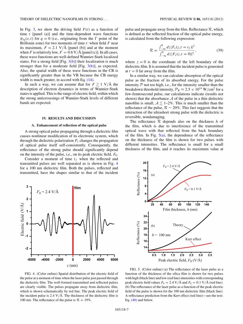
A strong optical pulse propagating through a dielectric filmcauses nonlinear modification of its electronic system, whichthrough the dielectric polarization Px changes the propagationof optical pulse itself self-consistently. Consequently, thereflectance of the strong pulse should significantly dependon the intensity of the pulse, i.e., on its peak electric field, F0.
Consider a moment of time tf when the reflected andtransmitted pulses are well separated as is shown in Fig. 4for a 100 nm dielectric film. Both the pulses, reflected andtransmitted, have the shapes similar to that of the incident
F0 = 2.4 V/Å
Ele
ctri
c fi
eld
(V/ Å
)
z (nm)
FIG. 4. (Color online) Spatial distribution of the electric field ofthe pulse at a moment of time when the laser pulse just passed throughthe dielectric film. The well-formed transmitted and reflected pulsesare clearly visible. The pulses propagate away from dielectric film,which is shown schematically by red line. The peak electric field ofthe incident pulse is 2.4 V/A. The thickness of the dielectric film is100 nm. The reflectance of the pulse is R = 19%.
pulse and propagate away from the film. Reflectance R, whichis defined as the reflected fraction of the optical pulse energy,is calculated from the following expression:
R =∫ 0−∞ dz|Fx(z,t = tf )|2∫ 0−∞ dz|Fx(z,t = 0)|2
, (39)
where z = 0 is the coordinate of the left boundary of thedielectric film. It is assumed that the incident pulse is generatedat t = 0 far away from the film.
In a similar way, we can calculate absorption of the opticalpulse as the fraction of its absorbed energy. For the pulseintensity P not too high, i.e., for the intensity smaller than thebreakdown threshold intensity, PB ≈ 2.5 × 10¹⁴ W/cm2 for afew-femtosecond pulse, our calculations indicate (results notshown) that the absorbance A of the pulse in a thin dielectricnanofilm is small, A � 1–2%. This is much smaller than thereflectance of the pulse, R ∼ 20%. This fact suggests that theinteraction of the ultrashort strong pulse with the dielectric isreversible, nondamaging.
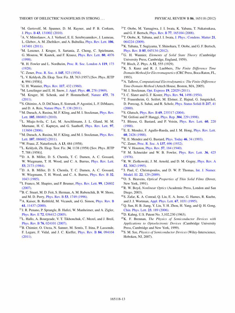
The reflectance R depends also on the thickness h ofthe film, which is due to interference of the transmittedoptical wave with that reflected from the back boundaryof the film. In Fig. 5(a), the dependence of the reflectanceon the thickness of the film is shown for two pulses withdifferent intensities. The reflectance is small for a smallthickness of the film, and it reaches its maximum value at
F0 = 0.1 V/Å
F0 = 2.4 V/Å
Theory
h = 100 nm
Peak electric field, F0 (V/Å)
Film thickness, h (nm)
Ref
lect
ance
(%)
Ref
lect
ance
(%)
(a)
(b)
Kerr effect
FIG. 5. (Color online) (a) The reflectance of the laser pulse as afunction of the thickness of the silica film is shown for two pulseswith high (black line) and low (red line) intensities with correspondingpeak electric field values F0 = 2.4 V/A and F0 = 0.1 V/A (red line).(b) The reflectance of the laser pulse as a function of the peak electricfield of the pulse is shown for the 100 nm dielectric film (black line).A reflectance prediction from the Kerr effect (red line)—see the text:Eq. (40) and below.
165118-7

VADYM APALKOV AND MARK I. STOCKMAN PHYSICAL REVIEW B 86, 165118 (2012)
a finite thickness h, which is a behavior characteristic of avery thin Fabry-Perot interferometer (this is a part of thefirst Fabry-Perot oscillation). This maximum is reached ath ∼ λ/neff , where neff is the effective refractive index ofthe film. In this maximum, an analytical solution of theMaxwell equations yields the following expression for thereflectance:44
Rmax ≈(
1 − n2eff
1 + n2eff
)2
. (40)
The reflectance shown in Fig. 5(a) increases fromR = 13%to R = 25% when the field amplitude increases from F0 =0.1 V/A to F0 = 3.5 V/A. This corresponds to the increase ofthe effective index (40) from neff = 1.46 to neff = 1.73, i.e.,the effective index change is �neff = 0.2. To compare, with theknown Kerr constant for silica45 n2 = 3.2 × 10⁻¹⁶ cm2/Wand the peak pulse power P0 = 1.6 × 10¹⁴ W/cm2 (corre-sponding to F0 = 3.5 V/A), the Kerr-effect increase of the in-dex would have been �neff = 0.05, i.e., significantly less thanpredicted by the present theory—see Fig. 5(b) where the blackcurve displays the theory prediction, and the red one showsthe Kerr-effect reflectance. This implies that in high fields thedielectric (silica) becomes much more polarizable (“softer”)than expected from the low-field behavior. This softening isinterpreted as a precursor to the adiabatic metallization,11,13
which is incomplete because the present field is too fast to beadiabatic.
In Fig. 6 we display polarization relative to the maximumpulse field χeff = Px/F0; note that εeff = max[4π |χeff|] is thecorresponding contribution to effective maximum permittivity.This relative polarization is computed for the midplane of ah = 100 nm nanofilm and for the optical pulse with peak valueof F0 = 2.4 V/A. This effective permittivity contribution issignificant, εeff ≈ 2.5, which again implies the field-inducedsoftening of the dielectric.
The increase of the refractive index in a strong externalelectric field of the optical pulse is due to generation ofnon-linear internal polarization, Px , of the system. Suchpolarization is determined by the nonlinear mixture of the
Elec
tric
Fiel
d (V
/Å)
Rel
ativ
e Po
lariz
atio
n, χ
eff
Time (fs)
FIG. 6. (Color online) Time-dependent relative polarizationχeff = Px/F0 for silica film of h = 100 nm thickness calculated fromEq. (30) for laser pulse with the amplitude of 2.4 V/A (black curve).Electric field of the pulse as a function of time (red curve). Both the po-larization and the field are calculated in the midplane of the dielectricfilm.
Adiabat
ic
Filled stateEmpty state
ħω nir-vi
sElectric field (V/Å)
Ener
gy (e
V)
Diabati
c
Filled stateEmpty state
ħω nir-vi
s
Electric field (V/Å)
Ener
gy (e
V)
(a)
(b)
FIG. 7. (Color online) Fragment of the adiabatic energy levelsof the nanofilm as function of the applied electric field. The verticalarrows indicate allowed dipole transitions in a near-infrared/visiblefrequency region. The arrows at the anticrossing points showpathways of the passage of the anticrossings. The open (filled) circlesdenote empty (filled) states. The line color codes the order of levelsin their energy. (a) Diabatic passage: at the anticrossing point thestates with the given quantum numbers preserve their population. Thecrossed arrows indicated the directions in which the population is pre-served. (b) Adiabatic passage: the population is conserved for both thelower and upper levels as indicated by the curved arrows. The bold redarrow shows the strongest transition that occurs between the parallellevels (terms) corresponding to the Wannier-Stark states localized atthe same lattice site, one of which is empty and the other populated.
states of the valence and conduction bands. Such a mixturecan be described in the basis of the Wannier-Stark states. Inthis basis, the interband coupling is a nonlinear function ofelectric field and is the strongest near the anticrossing pointsof the Wannier-Stark energy ladders.
To illustrate this effect, consider the adiabatic levels ofthe system (see Sec. III) shown in Fig. 7 where we display
165118-8

THEORY OF DIELECTRIC NANOFILMS IN STRONG . . . PHYSICAL REVIEW B 86, 165118 (2012)
a small fragment of the band diagram of Fig. 2 in anintermediate region of fields along with interband dipoletransitions denoted by the vertical arrows and population of thefilled and empty states indicated by filled and empty circles,respectively.
Figure 7(a) illustrates a case of the diabatic passage of thelevel anticrossings, where this passage occurs so rapidly thatthese anticrossings are ignored by the system. The conditionof the diabatic passage is δ � 1 where δ = hω/�ac is the so-called adiabatic parameter, and �ac is the anticrossing splittingenergy. In Fig. 7(a), the crossed arrows indicate the directionin which the populations and wave functions are preservedthrough the anticrossings. As one can see from the energyscale, in the vicinity of the anticrossings, there are allowedtransitions (i.e., those between the empty and filled levels) inthe near-infrared/visible (nir-vis) spectral region, i.e., withinthe spectral width of the excitation pulse. These transitions areresponsible for the polarization discussed above in conjunctionwith Fig. 6. As one can see, all the transitions in this case occurbetween the terms that are not parallel, which in accord withEq. (35) implies that the corresponding Wannier-Stark statesare localized at different lattice sites. Given that at such fieldsthese states are strongly localized (cf. Fig. 3), the overlap ofthe wave functions of such states localized at different sitesis relatively small. Therefore the dipole transitions betweenthem are suppressed and the corresponding polarization is notlarge. This appears to be the case for the conditions underconsideration.
The opposite limiting case of the adiabatic (i.e., for δ � 1)passage of the anticrossings is illustrated in Fig. 7(b). Inthis case, the population stays on a continuous line (term),as the curved arrows indicate, while the wave functions areexchanged when an anticrossing is passed. Such an exchangeimplies transfer of the electron population in space betweendifferent lattice sites. As a result, there are strong transitionsbetween parallel terms, i.e., between the Wannier-Stark stateslocalized at the same lattice site. One such a transitionis indicated by the bold red arrow in Fig. 7(b). Thesetransitions, which appear due to adiabatic population transfer,are analogous to those appearing due to metallization ofdielectric nanofilms.11,13
In Fig. 8, we show the temporal dynamics of the incidentpulse field (black curve) and that of the field inside thedielectric (at the mid plane of the nanofilm) shown by thered curve. This internal field is of importance since it self-consistently determines electron dynamics in the dielectric.This field is suppressed compared to the field of the incidentpulse due to reflection from the dielectric-vacuum interface.This reflection is enhanced because of the polarizability of thedielectric is increased due to the enhanced nonlinear effectsboth in the diabatic and adiabatic pathways—see above thediscussion of Fig. 7. Note that the internal field pulse (thered line) is almost (but not perfectly) symmetric with respectto its maximum point, which implies that the excitation ofthe dielectric by the strong field is almost reversible: verylittle population of the CB is left behind after the pulse ends.Nevertheless, there is some small but appreciable asymmetryof the internal field pulse with respect to its maximum: on thetrailing edge the internal field is somewhat smaller comparedto that at the leading edge implying that a relatively small
Ele
ctri
c fi
eld
(V/Å
)
Time (fs)
FIG. 8. (Color online) The electric field of the incident opticalpulse (black line) and the electric field at the midpoint of the dielectricfilm (red line) are shown as functions of time. The graphs are shiftedin time so that the maxima of two dependencies occur at the samemoment of time. The thickness of the film is 100 nm and the amplitudeof the laser pulse is F0 = 2.4 V/A.
population is left behind by the strong pulse—see also belowFig. 9 and its discussion.
B. Dynamics of electron system
The electric field of the optical pulse induces mixing ofthe electronic states of the VB and CB. The amplitudes foran electron to be in the VB or CB is given by projection ofits exact time-dependent wave function onto the unperturbed
Ele
ctri
c fi
eld
(V/Å
)
CB
pop
ulat
ion
(%)
Time (fs)
F0 = 2.4 V/Å
FIG. 9. (Color online) The time-dependent conduction bandpopulation, defined by Eq. (41), is shown for dielectric film withthe thickness of 100 nm. The amplitude of the pulse is 2.4 V/A. Theelectric field at the midpoint of the film is also shown. There is acorrelation between the the conduction band population and electricfield of the pulse. There is also small residual population, illustratingthat the electron system almost returns to the original state after thepulse passes through the film. The interband dipole matrix element isZvc = 3.0 eA.
165118-9

VADYM APALKOV AND MARK I. STOCKMAN PHYSICAL REVIEW B 86, 165118 (2012)
states of the corresponding band (VB or CB). The occupiedelectron states, which are initially the valence band states, arerepresented by wave functionsB(v) = (β(v)
v ,β(v)c ) [see Eq. (29)]
and have both the VB and CB components. The CB occupationNc(t) is given by
Nc(t) =∫
dz
∫dq
∣∣β(v)c (q,z,t)
∣∣2, (41)
where the integral over momentum q is extended over the firstBrillouin zone, and the z integral is extended over the nanofilmthickness. The conduction band population of Eq. (41) is afundamentally observable quantity, though in practice it maynot be easily measurable. Physically, Nc determines such aparticularly important effect as Pauli blocking of the VB toCB transitions.
The occupationNc of the CB states is shown in Fig. 9 for theinterband dipole parameter Zvc = 3.0 eA and amplitude of theoptical pulse F0 = 2.4 V/A. The conduction band occupationNc is clearly behaving as a function of the instantaneous elec-tric field of the pulse, more precisely of |F (t)|. This occupationhas its maximum values at the maxima and minima of the pulseelectric field. In addition to a smooth time-dependent part ofNc, which follows |F (t)|, there are also fast oscillations withfrequency close to the �g/h, where �g is the bandgap. Thereis also a small, ≈0.5%, residual population of the CB after thepulse passes through the film. This smallness of the residualpopulation is due to the circumstance that both the pure dia-batic and adiabatic passages of the anticrossings do not leavethe residual population. In our case, this residual population,as well as the fast population oscillations, are likely to be dueto impure diabatic passages (i.e., the passages that are fast butnot infinitely fast). Note that oscillations of a similar natureare also seen in the polarization and internal field—see Fig. 6.
Earlier in this section, we considered the electron dynamicsfor a fixed interband matrix element Zvc = 3 eA. There is anontrivial dependence of the electron dynamics on this matrixelement that we will discuss below.
In Fig. 10(a), results are shown for a relatively low dipoleinterband coupling, Zvc = 1.0 eA. For an anticrossing at �l =2 (the next-nearest neighbor), the anticrossing splitting (gap)is very small �ac ≈ 0.03 eV; correspondingly δ � 1, and thepassage is extremely diabatic. For the anticrossing at �l = 1(the nearest neighbor anticrossing, which occurs last as theelectric field increases), �ac ≈ 1 eV. With hω0 = 1.5 eV, δ ∼1, and the passage of this last anticrossing is intermediatebetween diabatic and adiabatic; consequently, one can expect asignificant residual CB population to occur (see also discussionbelow in Sec. V).
The corresponding dynamics of the CB population forthis low interband coupling matrix element Zvc = 1.0 eAis displayed in Fig. 11(a). As we see, both the maximumpopulation (at t ≈ 2 fs) and the residual CB population (fort > 6 fs) monotonously increase with the excitation fieldamplitude F0. The CB population (both maximum and resid-ual) becomes very large, Nc ≈ 20–40%, for F0 � 2.8 V/Aleading to an increased deposition of energy and possibledielectric breakdown.
The adiabatic levels for a larger dipolar coupling, Zvc =3.0 eA, are illustrated in Fig. 10(b). Note that anticrossingsfor a given �l are shifted to higher fields with respect to
Zvc = 1.0 eÅ
Zvc = 3.0 eÅ
Ene
rgy
(eV
) E
nerg
y (e
V)
Electric field (V/Å)
Electric field (V/Å)
(a)
(b)
Δl=1
Δl=2
Δl=1
Δl=2
FIG. 10. Adiabatic energy spectra of two-band system is shownas a function of external electric field for different values of Zvc:(a) Zvc = 1.0 eA, and (b) Zvc = 3.0 eA. The two bands are the VBand CB of silica with the energy gap �g = 9 eV. This two-bandsystem is finite and each band consists of 50 energy levels. Theanticrossing points with �l = 1 and �l = 2 are shown.
the case of low dipolar coupling [cf. Fig. 10(a)]. For theanticrossing at �l = 2, �ac ≈ 0.3 eV and δ ≈ 5; thus thepassage of this anticrossing is mostly diabatic. In contrast,for �l = 1, �ac ≈ 5 eV and δ ≈ 0.3; hence, this anticrossingis mostly adiabatic. However, it occurs at a very high fieldF0 = 3.5 V/A where electric breakdown is likely to occureven for such short excitation pulses [see also below in thediscussion of Fig. 12(b) and Sec. V].
The dynamics of the CB population for the case of largedipolar coupling, Zvc = 3.0 eA, is illustrated in Fig. 11(b).The most dramatic feature is the sharply reduced residualpopulation as compared to Fig. 11(a), Nc < 2% for all fields.This indicates high reversibility of the excitation in this case.The peak population is reached close to the maximum ofthe excitation pulse (t = 0); its value at the highest field issignificantly reduced comparing to the case of weak coupling.Physically, this counterintuitive behavior (the reduction of the
165118-10

THEORY OF DIELECTRIC NANOFILMS IN STRONG . . . PHYSICAL REVIEW B 86, 165118 (2012)
F0 = 1.6 V/ÅF0 = 1.2 V/Å
F0 = 2.4 V/Å
F0 = 3.6 V/Å
CB
pop
ulat
ion
(%)
Time (fs)
(b)
F0 = 1.6 V/ÅF0 = 2.4 V/Å
F0 = 2.8 V/Å
F0 = 3.6 V/Å
CB
pop
ulat
ion
(%)
Time (fs)
(a)
Zvc = 1.0 eÅ
Zvc = 3.0 eÅ
FIG. 11. (Color online) Time dependent CB population is shownfor different amplitudes of the laser pulse and different values ofparameter Zvc: (a) Zvc = 3.0 eA and (b) Zvc = 1.0 eA. The numbersnext to the lines are the corresponding amplitudes of the laser field.The thickness of the film is 100 nm. At Zvc = 1.0 eA (b) there isa large residual population of the conduction band, while at Zvc =3.0 eA (a) the residual population of the conduction band is small.
residual and maximum populations with respect to the caseof weak coupling) is related to fact that the WS anticrossingsoccur at a higher field, and the one within the range of fieldsconsidered (�l = 2) is highly diabatic, which prevents a largepopulation transfer.
The dependence of the CB population Nc on the dipolarcoupling constant Zvc at a fixed pulse amplitude F0 =2.4 V/A is displayed in Fig. 12(a). In the initial part of theexcitation pulse (t < −1 fs), i.e., for low excitation fields, thepopulation Nc monotonously increases with Zvc, as intuitionwould predict. At the pulse maximum, the dependence onZvc saturates but still is monotonous. In contrast, the residual(t > 6 fs) population dependence on the dipolar coupling isnonmonotonous. For a low coupling, Zvc = 0.5 − 1 eA, Nc
increases with Zvc, which is characteristic of the diabatic casewhere the coupling is mostly perturbative. Counterintuitively,with further increase of the coupling, Zvc > 1 eA, the residualpopulation decreases with increase of Zvc. This is related tothe fact that only the last anticrossing (the one with �l = 1),which can have a significant anticrossing gap, shifts to larger,unattainable fields. The anticrossing gaps for �l � 2 are verysmall and, consequently, the corresponding dynamics is deeplydiabatic. This deeply diabatic dynamics is mostly perturbativeand contributes little to the population transfer.
40
30
20
10
0.8 1.6 2.4 3.20M
ax C
B p
opul
atio
n (%
)
Peak electric field, F0 (V/Å)
Zvc = 1.0 eÅ
Zvc = 3.0 eÅ
(b)
Zvc = 0.5 eÅ
Zvc = 1.0 eÅ
Zvc = 2.0 eÅ
Zvc = 3.0 eÅ
Time (fs)
CB
pop
ulat
ion
(%)
-6 -4 -2 0 2 4 60
4
8(a)
FIG. 12. (Color online) Population of the CB versus time andpeak electric field. The thickness of the film is 100 nm. (a) Timedependent CB population is shown for a given amplitude of thelaser pulse, F0 = 2.4 V/A, and different values of parameter Zvc
as indicated. (b) The maximum CB population as a function of thepeak electric field F0 for two values of the interband dipole matrixelement Zvc = 1.0 eA (red curve) and Zvc = 3.0 eA (black curve).
The CB population Nc at its maximum value during thepulse determines the heat production and damage of thedielectric. This important quantity is displayed in Fig. 12(b)against the peak electric field for two typical values of theinterband dipole element Zvc. The free electron gas populatingCB is characterized by the ratio η = RT F /aB , where RT F isthe Thomas-Fermi screening radius and aB is the Bohr radius,
RT F = 2e√
m∗c (3n)1/6
π1/6h√
ε, (42)
aB = εh2
m∗ce
2, (43)
where n = 2Nc/a3 is the maximum CB electron density, ε ≈
2.3 is the silica permittivity, and m∗c is the electron effective
mass for the CB, whose experimental value is46 m∗c ≈ 0.86m.
The electron gas in the CB possesses metallic behaviorfor η � 1 which means that excitons are screened out, andthe electrons behave as a free gas. Judging from Fig. 12(b),such a behavior sets on for F0 � 2.5 V/A (irrespectively ofZvc) where Nc � 0.15 and, correspondingly [see Eqs. (42)and (43)], η � 1.2. Thus, F0 ≈ 2.5 V/A is the breakdownfield amplitude, which corresponds to the peak pulse intensity≈1.7 × 10¹⁴ W/cm2.
V. CONCLUDING DISCUSSION
Let us briefly summarize fundamentals and main results ofthis article. One of the main points is nondamaging character
165118-11

VADYM APALKOV AND MARK I. STOCKMAN PHYSICAL REVIEW B 86, 165118 (2012)
and reversibility of the interaction of intense and ultrashortlaser pulses with a dielectric. These are determined by themaximum and residual electron population, Nc, of the CB—see Figs. 11 and 12. In these figures, we can see that themaximum CB population grows dramatically to ∼20–40 %for the peak external field F0 = 2.4–3.6 V/A correspondingto the peak intensity ∼1.5 × 10¹⁴–3.4 × 10¹⁴ W/cm2. Thesenumbers are rather reliable because they relatively weaklydepend on the interband dipole matrix element Zvc whoseexact value is not precisely known. As we have shown at theend of Sec. IV B, it is likely that the metallic behavior ofthe electron gas in the CB and, correspondingly, breakdownoccur for the peak field F0 � 2.5 V/A or peak pulse intensity�1.7 × 10¹⁴ W/cm2.
Previously it has been predicted25 that for significantlylonger 16-fs pulses with a twice higher carrier frequencyof 3.1 eV the breakdown intensity is ≈1015 W/cm2. Thisis significantly higher than predicted by our calculationsfor ≈4-fs pulses of 1.55 eV frequency. This difference iseven more significant if one keeps in mind that the damagethreshold should considerably decrease with increasing thepulse length and carrier frequency. Notice that our coherentapproach is not applicable for such long pulses as 16-fs dueto importance of electron-electron scattering at such longtimes.
The effective reversibility of the pulse-film interaction ismostly determined by the residual CB population after the endof the pulse: such a low population implies that the next pulsewould feel almost the same system as the initial one. One hasto keep in mind that the residual CB population decays due toradiative interband transitions and lives for a very long time∼100 ps,47 which is many orders of magnitude longer than thecharacteristic times of the process of excitation and dephasingrelaxation considered in our article. In contrast to the maximumCB population, the residual one very significantly dependson the interband dipole matrix element Zvc—cf. Figs. 11(a)and 11(b) and also see Fig. 12. Interestingly enough, thedependence on Zvc is nonmonotonic: it is increasing forZvc � 1 eA and sharply decreasing for Zvc � 1 eA.
This highly nontrivial dependence is due to the fact that theresidual population of the conduction band is most efficientlycreated in the case intermediate between the pure adiabaticand diabatic regimes where the adiabatic parameter δ ∼ 1. Infact, in the extreme adiabatic case (δ � 1), the population atthe leading edge of the pulse is very efficiently transferredto the CB at the level anticrossing point, just as it happensin the process of the adiabatic metallization.11 However, atthe trailing edge the population transfer at the anticrossingpoint occurs in the reverse direction, to the VB, resultingin a very low residual CB population.13 Such reversibilityis generally characteristic of adiabatic processes. In theopposite limiting case of a very diabatic process (δ � 1),the anticrossings are largely ignored by the system, and verylittle population transfer occurs. Only in the intermediatecase, δ ∼ 1, there is a significant residual population of theCB as we have already discussed above in conjunction withFig. 10.
A major observable quantity in our work is reflectance ofthe strong ultrashort pulses from the dielectric nanofilm. Thepredicted reflectance of a pulse increases with the pulse peak
field F0 [Fig. 5(b)] much stronger than the perturbative theoryof Kerr effect suggests. This implies that the response of thenanofilm is deeply nonperturbative even in the range below thepresumed breakdown threshold F0 ≈ 2.5 V/A. Interestinglyenough, the waveform of the reflected pulse is almost identicalto that of the incident pulse. This is a consequence of thereversibility of the pulse interaction with the nanofilm underour conditions; if this interaction were not reversible, e.g.,if a significant electron population were accumulated in theCB toward the end of the pulse, then the trailing edge of thereflected pulse would be significantly higher than the leadingedge due to a plasma-like response.
The underlying cause of the high reflectivity is the “soft-ening” of the dielectric, i.e., a significant increase of itspolarizability, in the strong field, which is illustrated in Fig. 6.This softening is significant: the corresponding contributionto the maximum permittivity is large, εeff = 4π max[|χeff|] ≈2.5, which causes more than doubling the permittivity ofsilica. This is related to the allowed low-frequency transitionsbetween the adiabatic energy levels of the system in thevicinities of the anticrossings of the Wannier-Stark levelsshown in Fig. 7.
The phenomena described above in this article are drivenby the instantaneous pulse field rather than its intensity or fieldintegral (“area” of the pulse). This points toward a fundamentalpossibility of ultrafast (with bandwidth comparable to theoptical frequency) field effect devices based on dielectricssimilar to but much faster than the field effect transistors(FETs)48–50 fabricated from the much “softer” semiconduc-tors. To explain this analogy, in the case of the FET, thecharges at the gate electrode by their electrostatic field attractthe minority carriers causing the adjacent channel of the FETto conduct. Similarly, in our case the instantaneous electricfield of the light wave may be thought of as inducing theappearance of the carriers (electrons in the previously emptyconduction band and the respective holes in the valence band),which causes the dielectric to conduct.
To conclude, we have described a number of highlynonlinear (nonperturbative) phenomena in dielectric (silica)nanofilms subjected to nearly single-period strong opticalpulses whose field can be just below the predicted breakdownthreshold of ∼2.5 V/A. These results show possibility offundamental phenomena and applications based on fieldcontrol of dielectrics very much similar to the phenomenaoccurring in semiconductors used in field-effects transistors.The strong but short optical fields lead to the optical-electricsoftening of the dielectrics. These phenomena are defined bythe instantaneous optical field rather then the pulse intensity orits field integral. Thus these phenomena are among the fastestin optics.
ACKNOWLEDGMENTS
This work was supported by Grant No. DEFG02-01ER15213 from the Chemical Sciences, Biosciences andGeosciences Division and by Grant No. DE-FG02-11ER46789from the Materials Sciences and Engineering Division of theOffice of the Basic Energy Sciences, Office of Science, USDepartment of Energy.
165118-12
THEORY OF DIELECTRIC NANOFILMS IN STRONG . . . PHYSICAL REVIEW B 86, 165118 (2012)
1M. Gertsvolf, M. Spanner, D. M. Rayner, and P. B. Corkum,J. Phys. B 43, 131002 (2010).
2A. V. Mitrofanov, A. J. Verhoef, E. E. Serebryannikov, J. Lumeau,L. Glebov, A. M. Zheltikov, and A. Baltuska, Phys. Rev. Lett. 106,147401 (2011).
3M. Lenzner, J. Kruger, S. Sartania, Z. Cheng, C. Spielmann,G. Mourou, W. Kautek, and F. Krausz, Phys. Rev. Lett. 80, 4076(1998).
4R. H. Fowler and L. Nordheim, Proc. R. Soc. London A 119, 173(1928).
5C. Zener, Proc. R. Soc. A 145, 523 (1934).6L. V. Keldysh, Zh. Eksp. Teor. Fiz. 33, 763 (1957) [Sov. Phys. JETP6, 994 (1958)].
7G. H. Wannier, Phys. Rev. 117, 432 (1960).8M. Lenzlinger and E. H. Snow, J. Appl. Phys. 40, 278 (1969).9M. Kruger, M. Schenk, and P. Hommelhoff, Nature 475, 78(2011).
10S. Ghimire, A. D. DiChiara, E. Sistrunk, P. Agostini, L. F. DiMauro,and D. A. Reis, Nature Phys. 7, 138 (2011).
11M. Durach, A. Rusina, M. F. Kling, and M. I. Stockman, Phys. Rev.Lett. 105, 086803 (2010).
12L. Miaja-Avila, C. Lei, M. Aeschlimann, J. L. Gland, M. M.Murnane, H. C. Kapteyn, and G. Saathoff, Phys. Rev. Lett. 97,113604 (2006).
13M. Durach, A. Rusina, M. F. Kling, and M. I. Stockman, Phys. Rev.Lett. 107, 086602 (2011).
14W. Franz, Z. Naturforsch. A 13, 484 (1958).15L. Keldysh, Zh. Eksp. Teor. Fiz. 34, 1138 (1958) [Sov. Phys. JETP
7, 788 (1958)].16D. A. B. Miller, D. S. Chemla, T. C. Damen, A. C. Gossard,
W. Wiegmann, T. H. Wood, and C. A. Burrus, Phys. Rev. Lett.53, 2173 (1984).
17D. A. B. Miller, D. S. Chemla, T. C. Damen, A. C. Gossard,W. Wiegmann, T. H. Wood, and C. A. Burrus, Phys. Rev. B 32,1043 (1985).
18I. Franco, M. Shapiro, and P. Brumer, Phys. Rev. Lett. 99, 126802(2007).
19B. C. Stuart, M. D. Feit, S. Herman, A. M. Rubenchik, B. W. Shore,and M. D. Perry, Phys. Rev. B 53, 1749 (1996).
20A. Kaiser, B. Rethfeld, M. Vicanek, and G. Simon, Phys. Rev. B61, 11437 (2000).
21J. R. Penano, P. Sprangle, B. Hafizi, W. Manheimer, and A. Zigler,Phys. Rev. E 72, 036412 (2005).
22L. Hallo, A. Bourgeade, V. T. Tikhonchuk, C. Mezel, and J. Breil,Phys. Rev. B 76, 024101 (2007).
23B. Chimier, O. Uteza, N. Sanner, M. Sentis, T. Itina, P. Lassonde,F. Legare, F. Vidal, and J. C. Kieffer, Phys. Rev. B 84, 094104(2011).
24T. Otobe, M. Yamagiwa, J. I. Iwata, K. Yabana, T. Nakatsukasa,and G. F. Bertsch, Phys. Rev. B 77, 165104 (2008).
25T. Otobe, K. Yabana, and J. I. Iwata, J. Phys.: Condens. Matter 21,064224 (2009).
26K. Yabana, T. Sugiyama, Y. Shinohara, T. Otobe, and G. F. Bertsch,Phys. Rev. B 85, 045134 (2012).
27G. H. Wannier, Elements of Solid State Theory (CambridgeUniversity Press, Cambridge, England, 1959).
28F. Bloch, Z. Phys. A 52, 555 (1929).29K. S. Kunz and R. J. Luebbers, The Finite Difference Time
Domain Method for Electromagnetics (CRC Press, Boca Raton, FL,1993).
30A. Taflove, Computational Electrodynamics: The Finite-DifferenceTime-Domain Method (Artech House, Boston, MA, 2005).
31M. I. Stockman, Opt. Express 19, 22029 (2011).32J. C. Slater and G. F. Koster, Phys. Rev. 94, 1498 (1954).33T. Frauenheim, G. Seifert, M. Elstner, Z. Hajnal, G. Jungnickel,
D. Porezag, S. Suhai, and R. Scholz, Phys. Status Solidi B 217, 41(2000).
34S. Glutsch, Phys. Rev. B 69, 235317 (2004).35M. Grifoni and P. Hanggi, Phys. Rep. 304, 229 (1998).36J. Bleuse, G. Bastard, and P. Voisin, Phys. Rev. Lett. 60, 220
(1988).37E. E. Mendez, F. Agullo-Rueda, and J. M. Hong, Phys. Rev. Lett.
60, 2426 (1988).38E. E. Mendez and G. Bastard, Phys. Today 46, 34 (1993).39C. Zener, Proc. R. Soc. A 137, 696 (1932).40W. V. Houston, Phys. Rev. 57, 184 (1940).41P. M. Schneider and W. B. Fowler, Phys. Rev. Lett. 36, 425
(1976).42R. W. Ziolkowski, J. M. Arnold, and D. M. Gogny, Phys. Rev. A
52, 3082 (1995).43J. Paul, C. Christopoulos, and D. W. P. Thomas, Int. J. Numer.
Model. El. 22, 129 (2009).44O. S. Heavens, Optical Properties of Thin Solid Films (Dover,
New York, 1991).45R. W. Boyd, Nonlinear Optics (Academic Press, London and San
Diego, 2003).46S. Zafar, K. A. Conrad, Q. Liu, E. A. Irene, G. Hames, R. Kuehn,
and J. J. Wortman, Appl. Phys. Lett. 67, 1031 (1995).47Q. Sun, H. B. Jiang, Y. Liu, Y. H. Zhou, H. Yang, and Q. H. Gong,
Chin. Phys. Lett. 23, 189 (2006).48D. Kahng, U.S. Patent No. 3,102,230 (1963).49K. F. Brennan, The Physics of Semiconductor Devices with
Applications to Optoelectronic Devices (Cambridge UniversityPress, Cambridge and New York, 1999).
50S. M. Sze, Physics of Semiconductor Devices (Wiley-Interscience,Hoboken, NJ, 2007).
165118-13