mose and wse nanofilms with vertically aligned molecular layers … · mose2 and wse2 nanofilms...
TRANSCRIPT
MoSe2 and WSe2 Nanofilms with Vertically Aligned Molecular Layerson Curved and Rough SurfacesHaotian Wang,† Desheng Kong,‡ Petr Johanes,‡ Judy J. Cha,‡ Guangyuan Zheng,§ Kai Yan,‡ Nian Liu,∥
and Yi Cui*,‡,⊥
†Department of Applied Physics, Stanford University, Stanford, California 94305, United States‡Department of Materials Science and Engineering, Stanford University, Stanford, California 94305, United States§Department of Chemical Engineering, Stanford University, Stanford, California 94305, United States∥Department of Chemistry, Stanford University, Stanford, California 94305, United States⊥Stanford Institute for Materials and Energy Sciences, SLAC National Accelerator Laboratory, 2575 Sand Hill Road, Menlo Park,California 94025, United States
*S Supporting Information
ABSTRACT: Two-dimensional (2D) layered materials ex-hibit high anisotropy in materials properties due to the largedifference of intra- and interlayer bonding. This presentsopportunities to engineer materials whose properties stronglydepend on the orientation of the layers relative to thesubstrate. Here, using a similar growth process reported in ourprevious study of MoS2 and MoSe2 films whose layers wereoriented vertically on flat substrates, we demonstrate that thevertical layer orientation can be realized on curved and roughsurfaces such as nanowires (NWs) and microfibers. Such structures can increase the surface area while maintaining theperpendicular orientation of the layers, which may be useful in enhancing various catalytic activities. We show vertically alignedMoSe2 and WSe2 nanofilms on Si NWs and carbon fiber paper. We find that MoSe2 and WSe2 nanofilms on carbon fiber paperare highly efficient electrocatalysts for hydrogen evolution reaction (HER) compared to flat substrates. Both materials exhibitextremely high stability in acidic solution as the HER catalytic activity shows no degradation after 15 000 continuous potentialcycles. The HER activity of MoSe2 is further improved by Ni doping.
KEYWORDS: 2D material, MoSe2, WSe2, hydrogen evolution reaction, selenization
Two-dimensional (2D) materials have intrigued not onlyfundamental science study but also novel materials
engineering due to the unique physical and chemical proper-ties.1−10 Charge-neutral 2D molecular single layers with strongin-plane chemical bonds stack together via the weak van derWaals interaction to form the bulk material, introducing thehigh anisotropy and opening up the opportunities to developvarious methods of single layer materials synthesis.1,4,11−16
Besides the single layer flakes, many other interestingmorphologies such as thin films, nanoplates, nanoribbons,nanotubes, nanowires, and fullerene-like nanoparticles are madefrom 2D materials and show broad applications in a variety ofareas such as topological insulator,17−19 chemical and electro-chemical intercalation,8,20,21 electrocatalysis,22,23 and transis-tors.1,4,24 Most 2D materials studied that far including binarydichalcogenides such as MoS2 and graphene are inclined to beterminated by the basal planes to reduce the exposed edges dueto the inherently high surface energy of the edges. However,the edges of some 2D materials are catalytically active for manyimportant electrochemical reactions such as hydrodesulfuriza-tion,25 hydrogen evolution reaction (HER),22,26 and oxygen
reduction reaction.27 Exposing edges in these cases cantherefore boost the catalytic activities.Recently, we demonstrated thin films of vertically aligned
molybdenum disulfide (MoS2) and molybdenum diselenide(MoSe2) molecular layers on flat substrates.28 The edges ofMoS2 have been identified to be active sites for HERtheoretically and experimentally;22,26,29,30 thus, the maximallyexposed active edge sites showed large exchange currentdensities in HER.28 The synthesis of our vertically alignedlayers was through Mo reaction with sulfur or selenium vapor.It is proposed that at high temperatures the vapor diffusionalong the layers through van der Waals gaps is much faster thanthat across the layers; thus, the layers naturally orientperpendicularly to flat substrates to expose the edges.28
However, it is not clear whether such a rapid sulfurization orselenization reaction mechanism can be translated onto roughand curved surfaces. The rough and curved surfaces canincrease the surface area and maximize the exposed edge sites.
Received: May 28, 2013Revised: June 21, 2013
Letter
pubs.acs.org/NanoLett
© XXXX American Chemical Society A dx.doi.org/10.1021/nl401944f | Nano Lett. XXXX, XXX, XXX−XXX

Figure 1. Schematic of MoSe2 and WSe2 nanostructures. (A) Layered crystal structure of molybdenum (or tungsten) chalcogenide. Each charge-neutral layer consists of three covalently bonded atomic sheets, and the layers stack together along the c-axis by van der Waals interaction. (B)Molybdenum (or tungsten) chalcogenide nanofilm with molecular layers vertically standing on a flat substrate. The green color represents the edgesites, and the yellow color represents the terrace sites. (C) Molybdenum (or tungsten) chalcogenide nanofilm with molecular layers perpendicular toa curved surface. The edges are maximally exposed.
Figure 2. Characterization of MoSe2 nanofilm on a Si NW. (A) TEM image of MoSe2 nanofilm on a Si NW of 100 nm in diameter. (B) TEM imageof MoSe2 nanofilm on the curved surface of the Si NW with molecular layers perpendicular to the surface. On the basis of the TEM image, it appearsthat approximately 80% of the surface is covered with the edges. (C) Zoom-in TEM image of MoSe2 nanofilm on the Si NW. The film ispolycrystalline, and the grains are curved and around 10 nm in length and several nanometers in width. (D) The atomic vibration direction of A1gand E1
2g Raman modes of MoSe2. (E) Raman spectrum of MoSe2 nanofilm on Si NWs. The intensity ratio of MoSe2 A1g to E12g is around 13:1.
Nano Letters Letter
dx.doi.org/10.1021/nl401944f | Nano Lett. XXXX, XXX, XXX−XXXB

More interestingly, it may also induce strain, expanding orsqueezing the molecular layers and thus changing the electronicstructures of the films.31
Here we demonstrate that MoSe2 and tungsten diselenide(WSe2) nanofilms with molecular layers perpendicular to roughand curved surfaces can be synthesized by the rapid selenizationprocess, preferentially exposing the active edge sites for HER.We show significant improvement of HER activity of MoSe2and WSe2 on carbon fiber paper compared with the flat films.The vertically standing layers create strong bonds to thesubstrate, resulting in the extremely high electrochemicalstability against long-term potential cycling of 15 000 cycles.The HER catalytic activity of the MoSe2 catalysts was furtherimproved by increasing the thickness of the nanofilms ordoping with Ni atoms. WSe2, introduced here, is a novel HERcatalyst rarely explored previously.MoSe2 and WSe2 share similar crystal structures with MoS2
as shown in Figure 1A. The atoms covalently bond with eachother within single layers, which stack together by van derWaals interaction. Since the surface energy of the edge sites ismuch larger than that of the terrace sites, for example, in thecase of MoS2 the edge site surface energy is at least 2 orders ofmagnitude larger than the terrace site surface energy,32 it isenergetically nonfavorable to expose the edge sites on thesurface.22,25,26,33 A kinetically controlled rapid sulfurization orselenization process from our previous work overcomes thebarrier, and we synthesized MoS2 and MoSe2 flat films withmolecular layers perpendicular to the substrate, as shown inFigure 1B.28 The morphology is ideal for HER on a 2D surfaceby providing high density of edge sites, which have been provento be the active center of MoS2 for HER.
22,23,26,28,29,33−40 Tofurther increase the active edge sites per geometric area, the 2Dflat substrate might be replaced with high surface areasubstrates with 2D nanostructures or even 3D porousstructures. As illustrated in Figure 1C, making the molecularlayers stand on rough and curved surfaces and maximallyexposing the edge sites to boost the HER activity is of ourinterest.MoSe2 and WSe2 nanofilms were synthesized on Si
nanowires (NWs) with diameters ranging from 100 to 200nm (Supporting Information Figure S1). The Si NWs weregrown by vapor−liquid−solid (VLS) method using gold ascatalyst (see Methods).41 The 5 nm Mo or W films weredeposited onto Si NWs by DC magnetron sputtering, followedby a rapid selenization process at 600 °C in a horizontal tubefurnace where elementary selenium shots were used as theprecursors (see Methods).28 Because of the directionaldeposition, only half of the NW surface is covered with themetals. Figure 2A shows the transmission electron microscopy(TEM) image of a MoSe2 nanofilm on a Si NW of ∼100 nm indiameter. The dark contrast represents the MoSe2 nanofilm.Figure 2B shows that the curved surface of Si NW is covered byMoSe2 stripelike grains, with molecular layers perpendicular tothe NW surface to expose the edges. The edges are distinctalong the central axis of the NW because the electron beam isparallel to the vertically standing layers. Away from the centralpart of the NW, the layers are tilted away from the electronbeam; thus, fewer edges are observed. On the basis of TEMimages, it appears that approximately 80% of the surface iscovered with vertically aligned layers. At the sidewalls of theNW MoSe2 layers shoot out from the surface, again confirmingthe layers vertically stand along the curved surface.
A zoom-in TEM image is shown in Figure 2C. The grains arearound 10 nm long and several nanometers wide, growing inarbitrary directions but with c-axis parallel to the surface of theNW. This particular configuration results in a specific intensityratio of A1g (243 cm−1) to E1
2g (289 cm−1) Raman modesillustrated in Figure 2D,E.42,43 The Raman peak correspondingto the out-of plane Mo−Se phonon mode (A1g) is preferentiallyexcited for the edge-terminated film, which results in the muchhigher A1g peak intensity than the E1
2g peak intensity, as shownin Figure 2E (the intensity ratio of A1g to E1
2g is around13:1).28,32,44 The presence of Si NWs is confirmed by thestrong Raman peak at 523 cm−1.45 The WSe2 nanofilm on SiNWs shows similar results to the MoSe2 case, with a part of thecurved surface covered by vertically standing layers (SupportingInformation Figure S2).The demonstration of MoSe2 and WSe2 on Si NWs with
molecular layers perpendicular to the surface opens up theopportunity to maximally expose the HER active edge sites onhigh surface area substrates with curvature and roughness.Accordingly, the HER catalytic activity of MoSe2 and WSe2 isexpected to be largely improved. Carbon fiber paper is used asthe substrate which consists of conductive carbon fibers with anaverage diameter of 10 μm as illustrated in the scanningelectron microscopy (SEM) image in Figure 3A. In Figure 3B,
the whole surface of the carbon fiber is separated into roughand curved regions by several trenches, with small particle-likeprotrusions randomly distributed on the surface. 25 nm thickMo or W was directionally deposited onto the substrate by dcmagnetron sputtering, which was then converted into acorresponding diselenide film by rapid selenization process(see Methods). Figures 3C and 3D show the SEM images ofthe MoSe2 and WSe2 nanofilms on the carbon fibers,
Figure 3. SEM images of bare carbon fiber paper substrates andsubsequent MoSe2 and WSe2 nanofilms on the substrates. (A) SEMimage of carbon fiber paper in a large scale. The carbon fibers arehundreds of micrometers in length and around 10 μm in diameter.The junctions are fused together to ensure the conductance of thesubstrate. (B) SEM image of the rough and curved surface of carbonfiber. There are trenches along the z-axis separating the surface areainto several regions, with randomly distributed particles on it. (C, D)SEM images of MoSe2 and WSe2 nanofilms on carbon fiber paper. Thefilms are rough, and the trenches are still visible.
Nano Letters Letter
dx.doi.org/10.1021/nl401944f | Nano Lett. XXXX, XXX, XXX−XXXC
respectively. The nanofilms turn out to be rough but formcontinuous coatings on the fibers. The trenches observed inboth nanofilms may be related to the surface topographicfeatures of the carbon fibers in Figure 3B. Different from thesmooth films synthesized on the mirror polished glassycarbon,28 the nanofilms on the carbon fiber papers exhibitcluster structures inherited from the surface structures and localcurvatures of the fibers.The MoSe2 and WSe2 nanofilms were investigated by X-ray
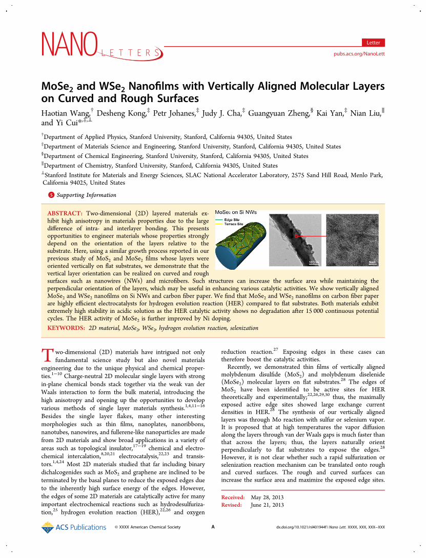
photoelectron spectroscopy (XPS) and Raman spectroscopyshown in Figure 4. The binding energies of Mo 3d5/2 and Mo3d3/2 are 228.6 and 231.8 eV in Figure 4A, respectively,revealing the +4 oxidation chemical state of Mo.33−36,38,46−48 Se3d5/2 and Se 3d3/2 located at 54.2 and 55.0 eV exhibit aroundthe same peak positions for both MoSe2 and WSe2, as shown inFigures 4B and 4D, indicating the same oxidation state of −2for Se in both materials.46−49 The peaks of W 4f7/2 (32.1 eV)and W 4f5/2 (34.2 eV) agree well with a previous study of WSe2thin films.49 The small peak at around 37.5 eV in Figure 4C isassigned as W 4f5/2 from WO3 due to the oxidation during the
sample preparation and transfer, and the W 4f7/2 from WO3 at35.7 eV is buried by the strong peak of W 4f5/2 from WSe2.Raman spectra provide information on the orientation of
MoSe2 and WSe2 molecular layers on the rough and curvedsurfaces of carbon fiber paper. The Raman modes A1g and E1
2g
of MoSe2 are indentified at 243 and 289 cm−1 in Figure 4E,respectively, sharing similar intensity ratio (A1g:E
12g = 13:1)
with that of MoSe2 nanofilm on Si NWs. The intensity ratioindicates that the MoSe2 molecular layers are vertically alignedon the carbon fibers, resulting in an edge-terminated nanofilmas designed in Figure 1C which is favorable to improve MoSe2HER catalytic activity. In addition, this special texture of thenanofilm not only makes full use of the high intralayerconductivity to reduce the impedance of the nanofilm(Supporting Information Figure S3) but also forms strongbonding with the substrate which may improve the stability ofthe nanofilm. The A1g and E1
2g modes of WSe2 are closelylocated at 253 and 250 cm−1, respectively.50 Accordingly, thetwo Raman mode peaks cannot be distinguished and only onebroad peak is observed in Figure 4F. However, the A1g peak canstill be identified as the stronger peak.50 Furthermore, the peak
Figure 4. XPS and Raman spectra of MoSe2 and WSe2 nanofilms on carbon fiber paper. (A, B) High-resolution XPS spectra of Mo 3d and Se 3dregions of MoSe2 nanofilm. (C, D) High-resolution XPS spectra of W 4f and Se 3d regions of WSe2 nanofilm. The WO3 peak is indicated by the redarrow. (E) A1g and E1
2g Raman modes of MoSe2 nanofilm. The intensity ratio of the two modes resembles that of the MoSe2 nanofilm on Si NWs.(E) A1g and E1
2g Raman modes of WSe2 nanofilm. The red dashed lines represent the position of two modes from a previous study.50
Nano Letters Letter
dx.doi.org/10.1021/nl401944f | Nano Lett. XXXX, XXX, XXX−XXXD
shares the same position and shape with that of WSe2 nanofilmon Si NWs (Figure S2); therefore, it is expected that the edgesof WSe2 are also preferentially exposed on the surface of carbonfiber paper.The HER catalytic activity of MoSe2 and WSe2 nanofilms on
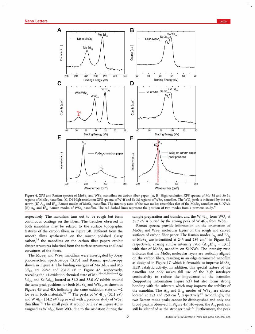
carbon fiber paper substrates are studied in 0.5 M H2SO4solution with a typical three-electrode electrochemical cellsetup. Electrochemical impedance spectroscopy (EIS) revealsnegligible ohmic resistance of the nanofilms (Figure S3). Sincethe electrochemical cell contains series resistances in the wiring,solution, and substrate, all of the data have been iR-corrected bysubtracting the ohmic resistance loss from the overpotential.The cathodic polarization curves of MoSe2 and WSe2 nanofilmson carbon fiber paper at a slow scan rate of 2 mV/s are shownin Figures 5A and 5B. In the MoSe2 electrode case, thereduction current density reaches 10 mA/cm2 at an over-potential around −250 mV, with much higher activity than thevertically aligned MoSe2 film grown on flat, mirror polishedglassy carbon in our previous study.28 Although WSe2 has loweractivity than MoSe2 with 50 mV larger overpotential to drivecathodic current density of 10 mA/cm2, it is still interestingbecause WSe2 has never been reported to be a goodelectrocatalyst for HER. Here WSe2 exhibits much higherHER activity than that of WS2 reported before.34,37,51 Noticethat WSe2 can be used as photocathode; our finding suggeststhe possibility to use WSe2 as both light absorber and HERcatalyst in photoelectrochemical cells.52−54
Tafel plots in Figure 5C are used to determine two importantparameters describing HER activity of catalysts: Tafel slope andexchange current density. The linear part of the MoSe2 Tafelplot under small overpotential is fitted to give a Tafel slope of
59.8 mV/dec, which is much smaller than the 120 mV/decfrom MoSe2 on mirror polished glassy carbon.28 The exchangecurrent density is determined to be 3.8 × 10⁻⁴ mA/cm2 byfitting the linear portion of the Tafel plot at low cathodiccurrent to the Tafel equation.22,28 Tafel slope is associated withthe elementary steps in HER. The first step of HER is adischarge step (Volmer reaction) in which protons areadsorbed to active sites on the surface of the catalysts andcombined with electrons to form adsorbed hydrogenatoms.26,40,55,56 It is followed by a combination step (Tafelreaction) or a desorption step (Heyrovsky reaction). In theprevious work the observed 120 mV/dec Tafel slope of MoSe2on flat glassy carbon substrate indicates that the rate-determining step was the discharge step, with a very smallsurface coverage of adsorbed hydrogen.28,56,57 In this work, itseems that the free energy barrier of the discharge step isreduced to be comparable with that of the following desorptionor combination step, resulting in the slope of 59.8 mV/dec.36,39
The surface curvature and roughness of the carbon fiber papersubstrate are likely to be responsible for the improved Tafelslope. The roughness and surface curvature may be able toexpand or squeeze the vertically standing molecular layers andthus change the electronic properties of the nanofilms, whichmay tune the reaction barriers effectively.28,33 WSe2 nanofilmon carbon fiber paper with a Tafel slope of 77.4 mV/dec alsoexhibits the facile HER kinetic process, which is a promisingcandidate in self-catalyzing HER in photoelectrochemicalcells.52−54
The structure of MoSe2 and WSe2 nanofilms with molecularlayers perpendicular to the substrates is beneficial to thestability of the catalysts due to the strong bonds between the
Figure 5. HER catalytic activities of MoSe2 and WSe2 nanofilms on carbon fiber paper. (A, B) Cathodic polarization curves of MoSe2 and WSe2nanofilms on carbon fiber paper compared with those on mirror polished glassy carbon as well as a blank carbon fiber paper substrate. (C) Tafelplots of MoSe2 and WSe2 nanofilms on carbon fiber paper. (D) Electrochemical stability test of MoSe2 and WSe2 in the cathodic potentials windows.
Nano Letters Letter
dx.doi.org/10.1021/nl401944f | Nano Lett. XXXX, XXX, XXX−XXXE

layers and the substrates. The extremely high stability of bothMoSe2 and WSe2 nanofilms is shown in Figure 5D. The as-grown catalysts were cycled by taking continuous cyclicvoltammograms (CV) between −0.28 and 0.1 V for MoSe2and −0.32 and 0.1 V for WSe2 vs RHE (before iR correction),respectively, over 15 000 cycles at a rate of 50 mV/s. The lowerpotential limits were set to reach a high cathodic currentdensity of 10 mA/cm2. We gently cleaned the surface of theMoSe2 and WSe2 catalysts and acquired polarization curvesevery 1000 CV cycles. The activities of both catalysts after 15000 cycles are slightly improved, likely due to the removal ofthe surface contaminates. The result confirms the extremelyhigh stability of MoSe2 and WSe2 catalysts on carbon fiberpaper. The SEM images of MoSe2 and WSe2 nanofilms oncarbon fiber paper after the cycling confirm that the nanofilmsare still tightly adhered to the carbon fibers, without any visibledegradation (Figure S4).The HER catalytic activity of the catalysts can be further
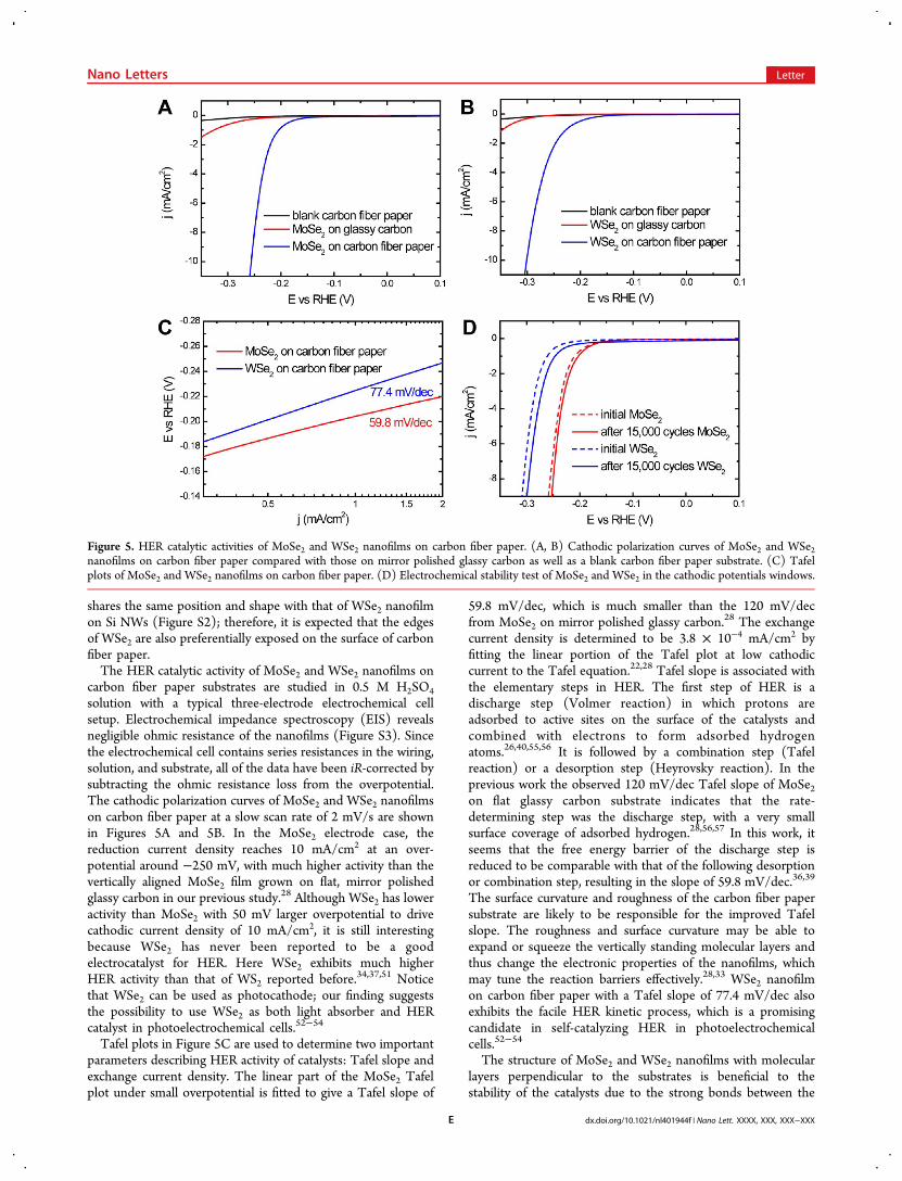
improved by increasing the thickness of the nanofilms. This isdemonstrated by MoSe2 shown in Figure 6. We deposited 50
nm of Mo onto the substrate, using the same procedure toconvert the Mo film into MoSe2. The thickness of the MoSe2nanofilm was around 200 nm. (Previously, we deposited 25 nmof Mo onto the carbon fiber paper, which resulted in ∼100 nmthick MoSe2 nanofilm.) The measured Tafel slope of thethicker MoSe2 nanofilm is maintained to be 63.9 mV/dec, butthe exchange current density is increased to 1.3 × 10⁻³ mA/cm2. Comparing with the thinner MoSe2 nanofilm, the thickerone may cover more surface area of the carbon fiber paper, andthe surface may also be rougher. However, the 200 nm thickMoSe2 nanofilm does not share the comparable stability withthe thinner one. The activity of the 200 nm MoSe2 nanofilmsubstantially decays after 1000 potential cycles (Figure S5). Thestability issue is associated with the poor mechanical adhesionof the active catalyst with the carbon fibers as revealed by theSEM images after cycling (Figure S6). Unlike the thinnerMoSe2 film, the thicker film does not bond to the substratestrongly enough and a large part of the film was easily peeledoff during the operation. We suspect that the induced strain ismuch larger for a thicker nanofilm which weakens the bondingto the substrate. It suggests the thickness of the nanofilm
should be optimized to balance the catalytic activity and thestability for long-term operation.It is known the incorporation of transition metals like Co, Ni,
and Fe into WS2 and MoS2 enhances their catalytic activity forHER.34,39 In the MoS2 case, the hydrogen binding energy at theMo-edge is smaller than that at the S-edge; accordingly, onlythe Mo-edge is catalytically active for HER.26,34,39 The Co-promoted S-edge significantly reduce the hydrogen binding freeenergy, making the S-edge active for HER.34,39 Inspired bythese theoretical calculations and experimental results, wedoped a small amount of Ni atoms into MoSe2 and explored itsinfluence on the catalytic activity. An additional 5 Å thick Niwas thermally evaporated onto the 5 nm Mo film on Si NWs,followed by the rapid selenization process. The TEM image ofthe Ni-doped MoSe2 nanofilm on Si NWs is shown in FigureS8, confirming that the vertically aligned MoSe2 molecularlayers were not affected by Ni doping. No Ni−Se clusters areobserved in the TEM image, indicating that the Ni atoms arehomogeneously incorporated into the MoSe2 matrix. To obtainthe HER catalytic activity, Ni-doped MoSe2 nanofilms weresynthesized on carbon fiber paper with 1 nm thick Ni thermallyevaporated onto 25 nm thick Mo film. Ni doping enhances theactivity by increasing the exchange current density to 2.8 ×10⁻³ mA/cm2 without affecting the Tafel slope (62.1 mV/dec).Accordingly, the Ni-doped catalyst achieves a cathodic currentdensity of 10 mA/cm2 with 30 mV lower overpotential than thepristine MoSe2 catalyst.In conclusion, we used the rapid selenization process to
synthesize MoSe2 and WSe2 on Si NWs and carbon microfiberswith molecular layers perpendicular to the curved and roughsurfaces. With the unique layer orientation that maximallyexposes the edge sites of the material, we produced highlyactive catalysts for HER. The catalytic activity of MoSe2 on thecurved and rough surfaces is demonstrated to be much higherthan that of MoSe2 on the flat substrate. WSe2 is introducedhere as a novel active HER catalyst which may function as bothlight absorber and HER catalyst in photoelectrochemical cells.Both materials exhibit extremely high stability thanks to thestrong bonding between the layers and the substrate. Theseedge-terminated layered catalysts can be readily applied indiverse water electrolysis devices as low-cost, high-performance,and stable HER catalysts.
Methods. Synthesis and Preparation. 30 nm thick Au filmwas thermally evaporated onto the Si substrate to be thecatalyst for Si NWs growth by the VLS method. Single-crystalline Si NWs were grown inside a tube furnace at 485 °Cfor 20 min, with silane (SiH4, 2% in Ar) flowed in at 80 sccmand hydrogen (H2, 99.999%) at 20 sccm with a total chamberpressure of 30 Torr. Edge-terminated MoSe2 and WSe2nanofilms on Si NWs and carbon fiber paper were growninside a single-zone, 12 in. horizontal tube furnace (Lindberg/Blue M) equipped with a 1 in. diameter quartz tube. Thesubstrates coated with Mo or W thin films were placed at thehot center of the tube furnace. Selenium shots (99.99%, fromAlfa Aesar) were placed on the upstream side of the furnace atcarefully adjusted locations to set the temperature. Ar gas wasused as the precursor carrier, and the pressure and flow ratewere kept at 1000 mTorr and 100 sccm, respectively, during thegrowth. The heating center of the furnace was quickly raised toreaction temperature of 600 °C in 15 min, and the seleniumprecursor was kept at around 300 °C. The furnace was held atreaction temperature for 15 min, followed by natural cool-down.
Figure 6. Further improvement of HER catalytic activity of MoSe2nanofilm on carbon fiber paper. The black line represents thepolarization curve of the pristine MoSe2 catalyst, the red one stands forthe double-thickness MoSe2 nanofilm, and the blue one is the Ni-doped MoSe2 nanofilm.
Nano Letters Letter
dx.doi.org/10.1021/nl401944f | Nano Lett. XXXX, XXX, XXX−XXXF

Characterizations. Characterizations were carried out usingtransmission electron spectroscopy (TEM, FEI Tecnai G2 F20X-Twin microscope at 200 keV), Raman spectroscopy (531 nmexcitation laser, WITEC Raman spectrometer), X-ray photo-electron spectroscopy (XPS, SSI SProbe XPS spectrometerwith Al Kα source), and scanning electron microscopy (SEM,FEI Nova NanoSEM 450).Electrochemical Studies. MoSe2 and WSe2 nanofilms were
grown on carbon fiber paper (from Fuel Cell Store) to measureHER activities. Electrochemically inert Kapton tape was used todefine the 1 cm2 electrode area. The measurements wereperformed in 0.5 M H2SO4 solution (deaerated by N2) using athree-electrode electrochemical cell setup, with a saturatedcalomel electrode (E(RHE) = E(SCE) + 0.279 V aftercalibration) as the reference electrode and a graphite rod(99.999%, from Sigma-Aldrich) as the counter electrode.
■ ASSOCIATED CONTENT*S Supporting InformationAdditional details on sample chracterizations, electrochemicalmeasurements, and analyses. This material is available free ofcharge via the Internet at http://pubs.acs.org.
■ AUTHOR INFORMATIONCorresponding Author*E-mail: [email protected] (Y.C.).NotesThe authors declare no competing financial interest.
■ ACKNOWLEDGMENTSWe acknowledge support by the Department of Energy, Officeof Basic Energy Sciences, Materials Sciences and EngineeringDivision, under Contract DE-AC02-76-SFO0515. Authorcontributions are as follows: H.W., D.K., and Y.C. conceivedthe experiments. H.W., P.J., and N.L. synthesized and preparedthe materials. H.W., D.K., J.J.C., and G.Z. performed character-izations. H.W., D.K., and P.J. carried out electrochemicalmeasurements and analyses. All authors contributed toscientific planning and discussions.
■ REFERENCES(1) Novoselov, K. S.; Geim, A. K.; Morozov, S. V.; Jiang, D.; Zhang,Y.; Dubonos, S. V.; Grigorieva, I. V.; Firsov, A. A. Science 2004, 306(5696), 666−669.(2) Novoselov, K. S.; Jiang, D.; Schedin, F.; Booth, T. J.; Khotkevich,V. V.; Morozov, S. V.; Geim, A. K. Proc. Natl. Acad. Sci. U. S. A. 2005,102 (30), 10451−10453.(3) Geim, A. K.; Novoselov, K. S. Nat. Mater. 2007, 6 (3), 183−191.(4) Radisavljevic, B.; Radenovic, A.; Brivio, J.; Giacometti, V.; Kis, A.Nat. Nanotechnol. 2011, 6 (3), 147−150.(5) Splendiani, A.; Sun, L.; Zhang, Y.; Li, T.; Kim, J.; Chim, C.-Y.;Galli, G.; Wang, F. Nano Lett. 2010, 10 (4), 1271−1275.(6) Hasan, M. Z.; Kane, C. L. Rev. Mod. Phys. 2010, 82 (4), 3045−3067.(7) Zhang, H.; Liu, C.-X.; Qi, X.-L.; Dai, X.; Fang, Z.; Zhang, S.-C.Nat. Phys. 2009, 5 (6), 438−442.(8) Mizushima, K.; Jones, P. C.; Wiseman, P. J.; Goodenough, J. B.Mater. Res. Bull. 1980, 15 (6), 783−789.(9) Tenne, R.; Margulis, L.; Genut, M.; Hodes, G. Nature 1992, 360(6403), 444−446.(10) Liu, Y.-H.; Porter, S. H.; Goldberger, J. E. J. Am. Chem. Soc.2012, 134 (11), 5044−5047.(11) Hernandez, Y.; Nicolosi, V.; Lotya, M.; Blighe, F. M.; Sun, Z.;De, S.; McGovern, I. T.; Holland, B.; Byrne, M.; Gun’Ko, Y. K.;
Boland, J. J.; Niraj, P.; Duesberg, G.; Krishnamurthy, S.; Goodhue, R.;Hutchison, J.; Scardaci, V.; Ferrari, A. C.; Coleman, J. N. Nat.Nanotechnol. 2008, 3 (9), 563−568.(12) Ramakrishna Matte, H. S. S.; Gomathi, A.; Manna, A. K.; Late,D. J.; Datta, R.; Pati, S. K.; Rao, C. N. R. Angew. Chem. 2010, 122 (24),4153−4156.(13) Reina, A.; Jia, X.; Ho, J.; Nezich, D.; Son, H.; Bulovic, V.;Dresselhaus, M. S.; Kong, J. Nano Lett. 2008, 9 (1), 30−35.(14) Balandin, A. A.; Ghosh, S.; Bao, W.; Calizo, I.; Teweldebrhan,D.; Miao, F.; Lau, C. N. Nano Lett. 2008, 8 (3), 902−907.(15) Kim, F.; Cote, L. J.; Huang, J. Adv. Mater. 2010, 22 (17), 1954−1958.(16) Eda, G.; Yamaguchi, H.; Voiry, D.; Fujita, T.; Chen, M.;Chhowalla, M. Nano Lett. 2011, 11 (12), 5111−5116.(17) Chen, Y. L.; Analytis, J. G.; Chu, J.-H.; Liu, Z. K.; Mo, S.-K.; Qi,X. L.; Zhang, H. J.; Lu, D. H.; Dai, X.; Fang, Z.; Zhang, S. C.; Fisher, I.R.; Hussain, Z.; Shen, Z.-X. Science 2009, 325 (5937), 178−181.(18) Peng, H.; Lai, K.; Kong, D.; Meister, S.; Chen, Y.; Qi, X.-L.;Zhang, S.-C.; Shen, Z.-X.; Cui, Y. Nat. Mater. 2010, 9 (3), 225−229.(19) Kong, D.; Randel, J. C.; Peng, H.; Cha, J. J.; Meister, S.; Lai, K.;Chen, Y.; Shen, Z.-X.; Manoharan, H. C.; Cui, Y. Nano Lett. 2009, 10(1), 329−333.(20) Shu, Z. X.; McMillan, R. S.; Murray, J. J. J. Electrochem. Soc.1993, 140 (4), 922−927.(21) Koski, K. J.; Cha, J. J.; Reed, B. W.; Wessells, C. D.; Kong, D.;Cui, Y. J. Am. Chem. Soc. 2012, 134 (18), 7584−7587.(22) Jaramillo, T. F.; Jorgensen, K. P.; Bonde, J.; Nielsen, J. H.;Horch, S.; Chorkendorff, I. Science 2007, 317 (5834), 100−102.(23) Chen, Z.; Cummins, D.; Reinecke, B. N.; Clark, E.; Sunkara, M.K.; Jaramillo, T. F. Nano Lett. 2011, 11 (10), 4168−4175.(24) Li, X.; Wang, X.; Zhang, L.; Lee, S.; Dai, H. Science 2008, 319(5867), 1229−1232.(25) Prins, R.; De Beer, V. H. J.; Somorjai, G. A. Catal. Rev. 1989, 31(1−2), 1−41.(26) Hinnemann, B.; Moses, P. G.; Bonde, J.; Jorgensen, K. P.;Nielsen, J. H.; Horch, S.; Chorkendorff, I.; Norskov, J. K. J. Am. Chem.Soc. 2005, 127 (15), 5308−5309.(27) Ahmed, S. M.; Gerischer, H. Electrochim. Acta 1979, 24 (6),705−711.(28) Kong, D.; Wang, H.; Cha, J. J.; Pasta, M.; Koski, K. J.; Yao, J.;Cui, Y. Nano Lett. 2013, 13 (3), 1341−1347.(29) Jaramillo, T. F.; Bonde, J.; Zhang, J.; Ooi, B.-L.; Andersson, K.;Ulstrup, J.; Chorkendorff, I. J. Phys. Chem. C 2008, 112 (45), 17492−17498.(30) Karunadasa, H. I.; Montalvo, E.; Sun, Y.; Majda, M.; Long, J. R.;Chang, C. J. Science 2012, 335 (6069), 698−702.(31) Allan, D. R.; Kelsey, A. A.; Clark, S. J.; Angel, R. J.; Ackland, G. J.Phys. Rev. B 1998, 57 (9), 5106−5110.(32) Verble, J. L.; Wietling, T. J.; Reed, P. R. Solid State Commun.1972, 11 (8), 941−944.(33) Kibsgaard, J.; Chen, Z.; Reinecke, B. N.; Jaramillo, T. F. Nat.Mater. 2012, 11 (11), 963−969.(34) Bonde, J.; Moses, P. G.; Jaramillo, T. F.; Norskov, J. K.;Chorkendorff, I. Faraday Discuss. 2008, 140 (0), 219−231.(35) Benck, J. D.; Chen, Z.; Kuritzky, L. Y.; Forman, A. J.; Jaramillo,T. F. ACS Catal. 2012, 2 (9), 1916−1923.(36) Merki, D.; Fierro, S.; Vrubel, H.; Hu, X. Chem. Sci. 2011, 2 (7),1262−1267.(37) Merki, D.; Hu, X. Energy Environ. Sci. 2011, 4 (10), 3878−3888.(38) Vrubel, H.; Merki, D.; Hu, X. Energy Environ. Sci. 2012, 5 (3),6136−6144.(39) Merki, D.; Vrubel, H.; Rovelli, L.; Fierro, S.; Hu, X. Chem. Sci.2012, 3 (8), 2515−2525.(40) Li, Y.; Wang, H.; Xie, L.; Liang, Y.; Hong, G.; Dai, H. J. Am.Chem. Soc. 2011, 133 (19), 7296−7299.(41) Chan, C. K.; Peng, H.; Liu, G.; McIlwrath, K.; Zhang, X. F.;Huggins, R. A.; Cui, Y. Nat Nanotechnol. 2008, 3 (1), 31−35.(42) Sekine, T.; Izumi, M.; Nakashizu, T.; Uchinokura, K.; Matsuura,E. J. Phys. Soc. Jpn. 1980, 49 (3), 1069.
Nano Letters Letter
dx.doi.org/10.1021/nl401944f | Nano Lett. XXXX, XXX, XXX−XXXG

(43) Wieting, T. J.; Verble, J. L. Phys. Rev. B 1971, 3 (12), 4286−4292.(44) Verble, J. L.; Wieting, T. J. Phys. Rev. Lett. 1970, 25 (6), 362−365.(45) Richter, H.; Wang, Z. P.; Ley, L. Solid State Commun. 1981, 39(5), 625−629.(46) Abdallah, W.; Nelson, A. E. J. Mater. Sci. 2005, 40 (9−10),2679−2681.(47) Pouzet, J.; Bernede, J. C. Rev. Phys. Appl. 1990, 25 (8), 807−815.(48) Ohuchi, F. S.; Parkinson, B. A.; Ueno, K.; Koma, A. J. Appl. Phys.1990, 68 (5), 2168−2175.(49) Boscher, N. D.; Carmalt, C. J.; Parkin, I. P. J. Mater. Chem. 2006,16 (1), 122−127.(50) Mead, D. G.; Irwin, J. C. Can. J. Phys. 1977, 55 (5), 379−382.(51) Sobczynski, A.; Yildiz, A.; Bard, A. J.; Campion, A.; Fox, M. A.;Mallouk, T.; Webber, S. E.; White, J. M. J. Phys. Chem. 1988, 92 (8),2311−2315.(52) McKone, J. R.; Pieterick, A. P.; Gray, H. B.; Lewis, N. S. J. Am.Chem. Soc. 2013, 135 (1), 223−231.(53) Boettcher, S. W.; Warren, E. L.; Putnam, M. C.; Santori, E. A.;Turner-Evans, D.; Kelzenberg, M. D.; Walter, M. G.; McKone, J. R.;Brunschwig, B. S.; Atwater, H. A.; Lewis, N. S. J. Am. Chem. Soc. 2011,133 (5), 1216−1219.(54) Liu, C.; Tang, J.; Chen, H. M.; Liu, B.; Yang, P. Nano Lett. 2013,in press.(55) Conway, B. E.; Tilak, B. V. Electrochim. Acta 2002, 47 (22−23),3571−3594.(56) Thomas, J. G. N. Trans. Faraday Soc. 1961, 57, 1603−1611.(57) Pentland, N.; Bockris, J. O. M.; Sheldon, E. J. Electrochem. Soc.1957, 104 (3), 182−194.
Nano Letters Letter
dx.doi.org/10.1021/nl401944f | Nano Lett. XXXX, XXX, XXX−XXXH