the study of chemical diffusion and properties of electric...
TRANSCRIPT

Charles University in Prague
Faculty of Mathematics and Physics
Doctoral Thesis
Nahlovskyy Bohdan Vasyl’ovych
The study of chemical diffusion and properties of
electric contacts on CdTe for gamma ray detector
applications
Institute of Physics of Charles University
Supervisor: Doc. RNDr. Roman Grill, CSc.
Branch: Quantum Optics and Optoelectronics
2010

dedicated to my brother
i

Acknowledgements
I express my deep gratitude to my supervisor Doc. RNDr. Roman Grill, CSc. for
his guidance through the whole period of my study. I am grateful for his kindness,
understanding and willingness to help. Our frequent discussions of various scientific
problems were great sources of knowledge and inspiration for me. His contribution
into the explanation of the experimental results and creating theoretical models were
vital for this work.
It was a great honour for me to work in the group of Prof. RNDr. Pavel Hoschl,
DrSc. and I am very grateful to him for his big support during my doctoral study.
I would like to express my sincere thanks to Doc. Ing. Jan Franc, DrSc. and
Ing. Eduard Belas, CSc. for excellent guidance at the beginning of my research
work, providing valuable advises concerning research.
I am grateful to Doc. RNDr. Pavel Moravec CSc. who has provided assistance
in constructing experimental set-up. His contribution into tuning equipment and
planing experiment allowed to optimize measurements and obtain novel data.
I am thankful to Prof. RNDr. Ing. Josef Sikula, DrSc. from CNRL (VUT,
Brno) for kind offer to exploit equipment for capacitance-voltage measurements and
for the valuable discussion of the obtained results.
I would like to acknowledge Roman Fesh, Karol Strecko, Vera Polakova, Milos
Cerny and all other workers of the Institute of Physics of Charles University in
Prague for their help in my research and study.
I am especially grateful to my parents for their love, inspiration and support.
I hereby declare, that I wrote my doctoral thesis by myself using exclusively cited
sources. Loan allowance granted.
Prague, 2010 Nahlovskyy B.V.
ii

Contents
Introduction v
1 CdTe: Review 1
1.1 Crystal structure . . . . . . . . . . . . . . . . . . . . . . . . . . . . . 1
1.2 Band structure . . . . . . . . . . . . . . . . . . . . . . . . . . . . . . 1
1.3 Crystal growth methods . . . . . . . . . . . . . . . . . . . . . . . . . 4
1.4 Defects . . . . . . . . . . . . . . . . . . . . . . . . . . . . . . . . . . . 10
1.5 Electric transport properties . . . . . . . . . . . . . . . . . . . . . . . 13
1.6 Application . . . . . . . . . . . . . . . . . . . . . . . . . . . . . . . . 14
2 Diffusion in CdTe 16
2.1 Interdiffusion . . . . . . . . . . . . . . . . . . . . . . . . . . . . . . . 17
2.2 Cd diffusion . . . . . . . . . . . . . . . . . . . . . . . . . . . . . . . . 18
2.3 Te diffusion . . . . . . . . . . . . . . . . . . . . . . . . . . . . . . . . 19
2.4 Chemical diffusion in CdTe:Cl . . . . . . . . . . . . . . . . . . . . . . 20
3 Metal-semiconductor junction 22
3.1 Energy band diagram . . . . . . . . . . . . . . . . . . . . . . . . . . . 22
3.2 Thermal equilibrium . . . . . . . . . . . . . . . . . . . . . . . . . . . 24
3.3 Forward and reverse bias . . . . . . . . . . . . . . . . . . . . . . . . . 25
3.4 Poisson equation . . . . . . . . . . . . . . . . . . . . . . . . . . . . . 27
3.5 Full depletion approximation . . . . . . . . . . . . . . . . . . . . . . . 27
3.6 Schottky diode current . . . . . . . . . . . . . . . . . . . . . . . . . . 30
3.6.1 Diffusion current . . . . . . . . . . . . . . . . . . . . . . . . . 30
3.6.2 Thermionic emission . . . . . . . . . . . . . . . . . . . . . . . 31
3.6.3 Tunnelling . . . . . . . . . . . . . . . . . . . . . . . . . . . . . 32
4 Surface chemical treatment 33
4.1 Etching compositions with bromine . . . . . . . . . . . . . . . . . . . 33
4.2 Etching compositions with iodine . . . . . . . . . . . . . . . . . . . . 35
4.3 Etching compositions with nitric acid . . . . . . . . . . . . . . . . . . 36
4.4 Etching compositions with hydrogen peroxide . . . . . . . . . . . . . 38
4.5 Etching compositions with bases . . . . . . . . . . . . . . . . . . . . . 38
iii

5 Experiment 40
5.1 Crystal growth . . . . . . . . . . . . . . . . . . . . . . . . . . . . . . 40
5.2 Sample preparation . . . . . . . . . . . . . . . . . . . . . . . . . . . . 42
5.3 Surface treatment . . . . . . . . . . . . . . . . . . . . . . . . . . . . . 43
5.3.1 Etching techniques . . . . . . . . . . . . . . . . . . . . . . . . 43
5.3.2 Surface roughness study . . . . . . . . . . . . . . . . . . . . . 44
5.4 Contact preparation . . . . . . . . . . . . . . . . . . . . . . . . . . . 44
5.4.1 Welding wires for the high-temperature measurements . . . . 44
5.4.2 Chemical deposition of metals . . . . . . . . . . . . . . . . . . 46
5.4.3 Thermal evaporation of metals . . . . . . . . . . . . . . . . . . 47
5.5 Electrical measurements . . . . . . . . . . . . . . . . . . . . . . . . . 47
5.5.1 Hall effect . . . . . . . . . . . . . . . . . . . . . . . . . . . . . 48
5.5.2 Conductivity . . . . . . . . . . . . . . . . . . . . . . . . . . . 48
5.5.3 Diffusion (through the conductivity) . . . . . . . . . . . . . . 50
5.5.4 Current-voltage characteristics . . . . . . . . . . . . . . . . . . 51
5.5.5 Capacitance-voltage . . . . . . . . . . . . . . . . . . . . . . . 54
5.5.6 Resistivity mapping . . . . . . . . . . . . . . . . . . . . . . . . 54
6 Results & Discussions 56
6.1 Sample characterization . . . . . . . . . . . . . . . . . . . . . . . . . 56
6.1.1 Resistivity mapping . . . . . . . . . . . . . . . . . . . . . . . . 56
6.1.2 Surface topology . . . . . . . . . . . . . . . . . . . . . . . . . 56
6.2 Chemical diffusion in bulk CdTe:Cl . . . . . . . . . . . . . . . . . . . 61
6.3 Properties of the contacts . . . . . . . . . . . . . . . . . . . . . . . . 67
6.3.1 Three-terminal versus two-terminal I-V technique . . . . . . . 67
6.3.2 Comparison of various metals as contact materials . . . . . . . 68
6.3.3 Contact quality depending on the etching solution used for
surface treatment . . . . . . . . . . . . . . . . . . . . . . . . . 75
6.3.4 Models of the anomalous concave shape of current-voltage
characteristic under forward bias . . . . . . . . . . . . . . . . 83
6.3.5 Capacitance-voltage measurements . . . . . . . . . . . . . . . 90
6.4 Detector response . . . . . . . . . . . . . . . . . . . . . . . . . . . . . 94
Conclusions 97
References 99
iv
Introduction
Nowadays gamma ray detectors are used in various aspects of our life, including
environmental [1] and security monitoring, nuclear science [2], and medical imaging
[3]. Demands to the quality and accessibility at a reasonable cost of these devices
increase every day. Medical applications are strictly limited by radiation dose living
tissue can be exposed to. In security purposes, size and resolution are of main
importance. Hence, detectors are required to be extremely sensitive, to have high
image resolution, be portable and non fastidious in operation.
Semi-insulating (SI) cadmium telluride (CdTe) has long been known to have
great potential in room-temperature gamma ray semiconductor detector applica-
tions [4, 5]. It has number of advantages over other semiconductor detectors used for
the same purposes (Ge, GaN). High atomic numbers of both components (ZCd=48,
ZTe=52) makes it much more effective in radiation-atomic interaction. Large enough
band gap (1.5 eV ) at room temperature provides high resistivity (above 109 Ω · cm)
of the intrinsic material and therefore a low leakage current, critical for the high
signal to noise ratio. High mobility of electrons (∼ 1100 cm2/V s at 300 K) allows
to reach a high intrinsic µτ (mobility-lifetime) product and therefore a high degree
of charge collection and a good spectral resolution. The full potential of this com-
pound for high-energy photon detection applications, however, was not exploited
for many decades due to the limited commercial availability of high-quality crys-
tals [4]. This situation has changed dramatically during the mid nineties with the
emergence of few companies committed to the advancement and commercialization
of CdZnTe based radiation detector technology. Companies Endicott Interconnect
Technologies, Inc. (U.S.A.), ACRORAD Company Ltd. (Japan), Nippon Mining &
Metals Co. Ltd. (Japan), LETI-CEA (France), Redlen Technologies (Canada) offer
large single-crystals grown by high pressure Bridgman (HPB) or travelling heater
methods (THM).
Still, the growth of large single-crystals of CdTe is state-of-the art process. Con-
ditions, under which high quality crystals grow, are not suitable for obtaining high
resistivity material. Even ingots grown from 7N purity initial materials have free
carriers concentration much higher than allowed maximum of 107 cm−3. To achieve
SI CdTe, the compensation of unintentional impurities and native defects by the
pinning of the Fermi level to some deep level near the middle of the band gap is
v
necessary. However, high density of doping defects significantly increases trapping
and recombination centres concentration, which decreases detection ability [6]. An-
other possibility to compensate native point defects (NPD) and decrease level of
needed doping is the annealing in the atmosphere of one of the components to get
stoichiometric composition.
Another problem of semiconductor gamma ray detectors is the leakage current.
When it is comparative with the effective current going through the device, huge
amount of signal is lost. Hence, sensitivity decreases significantly. Surface conduc-
tivity is responsible for the appearance of leakage current as well. By an appropriate
surface treatment it is possible to overcame this problem. Surface treatment greatly
influences the quality of contacts and properties of the metal-semiconductor junc-
tion.
The aim of this work is to investigate mass diffusion processes which occur in
CdTe at temperatures above 500 C and to find the conditions to obtain material
with required properties. Study is done indirectly through the observation of changes
in the material conductivity depending on the changes of the component vapour
pressure.
The second part of the thesis concerns with surface treatment in various etching
solutions, which is studied in detail first to get surfaces much more resistive than
bulk material, second to prepare ohmic contacts to be used as electrodes. Three-
terminal technique is employed for the measurement and results are compared with
more common two-terminal method. Capacitance-voltage experiment is used to
obtain additional information about contact properties.
vi

Chapter 1
CdTe: Review
1.1 Crystal structure
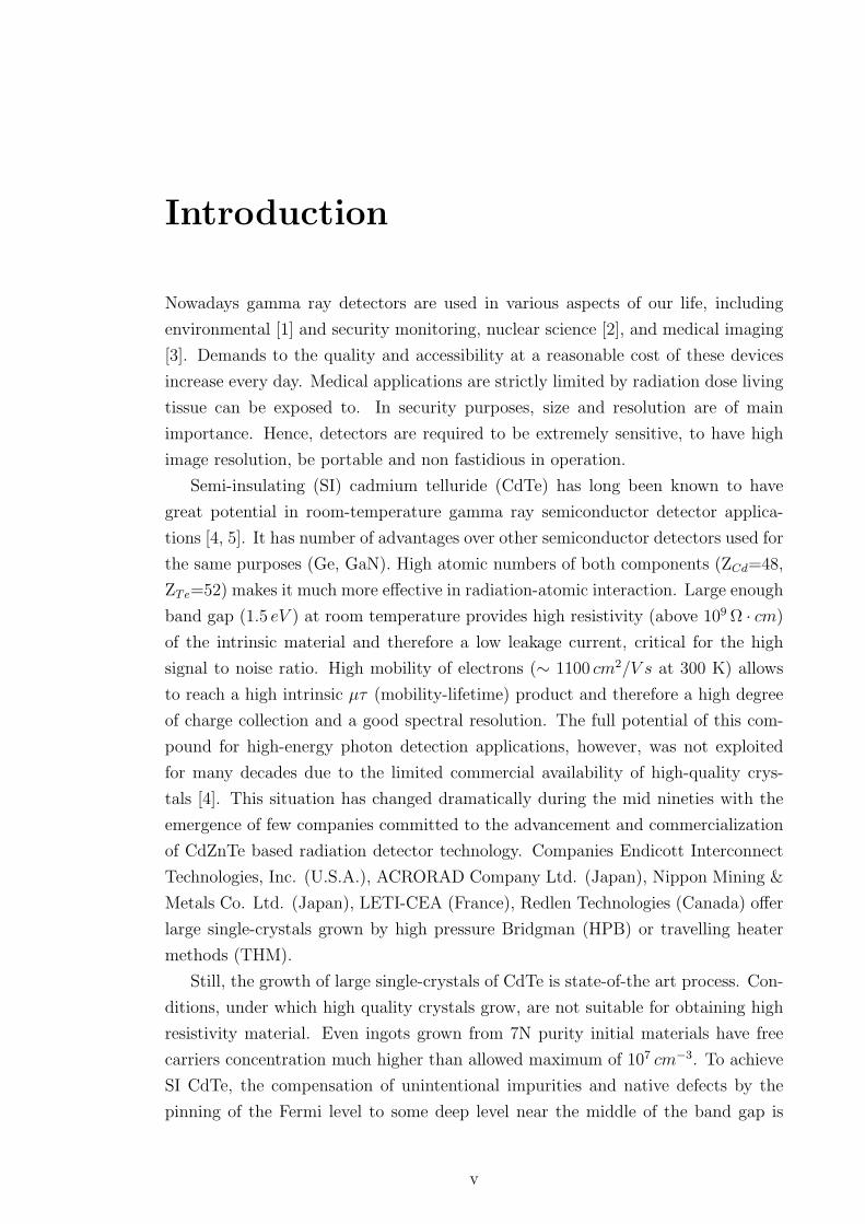
Cadmium telluride belongs to the AIIBIV group of semiconductors with a cubic
zincblende crystal structure (Figure (1.1)). This structure is described as a pair
of inter-penetrating face centred cubic (fcc) sub-latices of each element, Cd and
Te, offset from each other by one quarter of a unit cell body diagonal. The space
group of this structure is called F 43m (in Hermann-Mauguin notation), or 216 in
the International Tables for Crystallography.
The room temperature lattice parameter of CdTe is the largest among the AIIBIV
compounds and depends on the deviation from stoichiometry. It varies from 6.480A
for crystals grown from Cd-rich melt to 6.488A for grown from Te-rich one [7].
Recently, in research conducted on samples quenched after annealing, it was shown
that the lattice parameter decreases with increasing deviation from stoichiometry for
both Te- and Cd-rich cadmium telluride [8]. The lattice parameter of stoichiometric
CdTe was reported to be 6.4825 A.
Chemical bonds between cadmium and tellurium atoms are characterized as
intermediate to ionic and covalent. They are formed by the Cd 5s2 and Te 5s25p4
electrons. Atomic orbitals are mixed and form new sp3 hybrid orbitals.
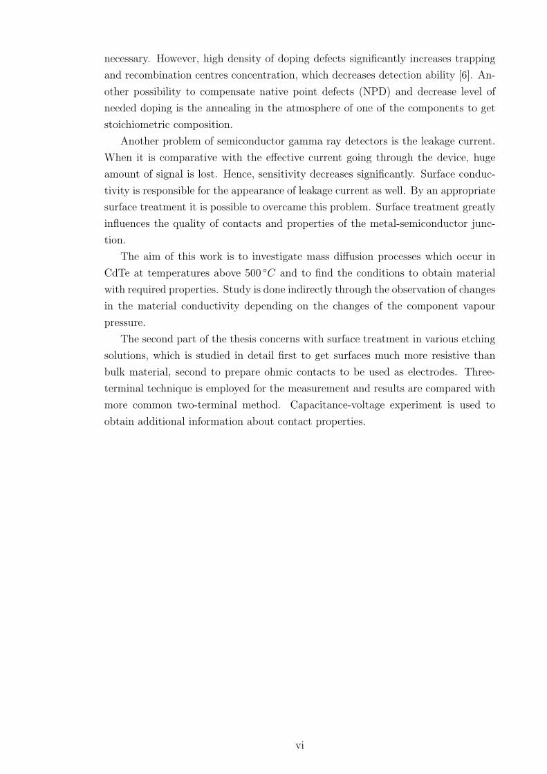
The shape of the Brillouin zone of zincblende structure is a truncated octahedron
(Figure (1.2)) with fourteen plane faces, six square faces along the [100] direction
and eight hexagonal faces along [111] direction.
1.2 Band structure
CdTe has a direct energy band structure with a minimum of the conduction band
and maximum of the valence band in the centre of Brillouin zone, Γ point.
The Kane model [9] is used to calculate the band structure. In this model atomic
wave function and the spin of electron are taken into consideration. Interactions,
which determine the heavy hole effective mass are not included in the simplified
1
Figure 1.1: Zincblende crystal structure. The arrangement of atoms is the sameas in diamond cubic structure, but with alternating types of atoms at the differentlattice sites.
z
k
k
k
K W
XU
L Q
U'
X'
Z
x
y
Figure 1.2: Brillouin zone of zincblende structure.
2

4
2
0
-2
-4
-6
-8
-10
-12
L X U,K
E,
eV
Figure 1.3: Cadmium telluride band structure diagram.
Kane’s model.
The valence band structure consists of three bands, two of them are degenerated
at ~k = 0. The third sub-band is split-off by the spin orbit coupling. The split-of
energy at ~k = 0 is denoted by ∆. The conduction and valence band dispersion can
be approximated by the following forms:
• conduction band
E − Eg =~2k2
2m0
+1
2
(√E2
g +8P 2k2
3− Eg
)(1.1)
where P is Kane’s matrix element (P = 8× 10⁻⁸ eV cm),
• valence band
– heavy holes
E = −~2k2
2mh
(1.2)
– light holes
E =~2k2
2m0
− 1
2
(√E2
g +8P 2k2
3− Eg
)(1.3)
3

– split-off band
E = −∆ +~2k2
2m0
− P 2k2
3(Eg + ∆)(1.4)
where ∆ = 0.8 eV.
As can be seen in Figure (1.3) the conduction band and the light hole valence band
are non-parabolic. That means that E is not simply proportional to k2.
The value of the forbidden gap depends on the temperature. Various authors
investigated the energy gap temperature dependence of CdTe. According to Brebrick
[10]:
Eg = 1.70− 5.345× 10⁻⁴T, eV. (1.5)
D. Nobel [11] gives different equation:
Eg = 1.622− 3.5× 10⁻⁴T − 1.1× 10⁻⁷T 2, eV. (1.6)
CdTe has relatively wide band gap which allows to use non-degenerate statistics
for moderate carrier concentration. The low effective mass of the electron (me =
0.096m0) in CdTe results in good transport properties of electrons.
1.3 Crystal growth methods
A large diameter CdTe single crystals are strongly desired for the application in
semiconductor technology. The ingots are sliced with an inner diameter diamond
coated blade and polished to form wafers. A wafer is a thin slice of material used
in the fabrication of integrated circuit and other micro-devices. The wafer serves as
the substrate for microelectronic devices built in and over the wafer and undergoes
to many micro-fabrication process steps such as doping or ion implantation, etching,
deposition of various materials, and photo-lithographic patterning. Requirements
to the crystals’ quality are very high. Wafers are formed of high purity (99.9999%),
nearly defect-free single crystalline material. Crystal diameter is important as well.
The larger the wafer, the less space on the edges as a percentage of total space. This
means, less of the wafer is un-etched, and in theory should have higher productivity.
This is the basis of shifting to larger and larger wafer sizes.
There is no single best method of crystal preparation. A number of them were
developed. Each of this method has its advantage and disadvantage and the growth
technique is chosen depending on various parameters.
• Czochralski method
For many semiconductor materials pulling from the melt by the Czochralski
method (Figure 1.4) is the dominant technique for obtaining single crystals. A
seed crystal, mounted on a rod, is dipped into the molten material. The seed
4

4
5
1
2
3
x
TTM
Figure 1.4: Temperature profile and schematic graph of the Czochralski process. TM
- melting point temperature; 1 - crucible; 2, 3 - rods, rotated in opposite directions;4 - ingot; 5 - melt.
crystal’s rod is pulled upwards and rotated at the same time. By precisely
controlling the temperature gradients, rate of pulling and speed of rotation,
it is possible to extract a large, single-crystal, cylindrical ingot from the melt.
Occurrence of unwanted instabilities in the melt can be avoided by investi-
gating and visualizing the temperature and velocity fields during the crystal
growth process. This process is normally performed in an inert atmosphere,
such as argon, and in an inert chamber, such as quartz.
High cadmium vapour pressure does not allow to use this method directly
for CdTe growth. Its modification, liquid encapsulated Czochralski (LEC)
[12, 13] in which liquid encapsulation prevents the loss of volatile Cd, can
be used instead. However, despite LEC has been proven to be suitable for
several other compound semiconductors, it has not succeeded for CdTe. Its
disadvantage is in large temperature non-linearities and large temperature
gradients causing high thermal stress in the growing crystal.
• Vapour growth method
Growth process under this technique is performed at temperatures lower that
the material melting point. The crystals are grown in a closed crucible which
is moved through a step temperature gradient [14, 15]. The source material
is always hotter than the growing surface as shown on Figure (1.5). Thus,
mass transport occurs from the source to the crystal. The extended growth
5

T
x
1 2 3
Figure 1.5: Schematic graph and temperature profile of the vapour phase growthtechnique. 1 - quartz ampoule; 2 - charge; 3 - crystal.
period allows the defects to reach a state of equilibrium, where most of the
dislocations content is concentrated in sub-grain boundary walls. This method
is used to growth CdZnTe with different compositions.
• Travelling heater method
Float-zone method was initially developed for the crystal purification. Latter
it was found to be suitable for the crystal growth.
Material obtained from float-zone technique is a high-purity alternative to
crystals grown by the Czochralski process. The concentrations of impurities,
such as carbon and oxygen, are extremely low. impurity The dimensions of
float-zone wafers are generally less than 150 mm due to the surface tension
limitations during growth. A radio-frequency (RF) field is used to produce
a local melted zone on the polycrystalline rod that is dragged from one end
to the other. Float-zone pulling is shown on Figure (1.6). Seed crystal is
used at one end in order to start the growth. The whole process is carried
out in an evacuated chamber or in an inert gas purge. The molten zone
carries the impurities away with it and hence reduces impurity concentration
(impurities are mostly more soluble in the melt than in crystal). Specialized
doping techniques like: Core doping, Pill doping, Gas doping and Neutron
transmutation are used to incorporate a uniform concentration of dopant.
The growth rate is very slow, about 5 mm/day, to prevent supercooling. That
6

TT
x
M
1
2
3
4
5
6
Figure 1.6: Temperature profile and schematic graph of the float-zone growthmethod. TM - melting point temperature; 1 - feed rod holder; 2 - seed rod holder;3 - RF heating coil; 4 - feed rod; 5 - single crystal; 6 - molten zone.
is why this method is not appropriate for the growth of large crystals. Ingots,
obtained by this method, usually have several grains. Therefore, this tech-
nique is effective for manufacturing of high purity crystals with large grains
for devices based on small chips such as radiation detectors.
• Vertical gradient freeze method
Gradient freeze method along with Bridgman method are the most frequently
used for melt growth of CdTe and related compounds. The vertical modifica-
tion, called Vertical Gradient Freeze, is preferred in industrial use because of
higher demand on round wafers.
The method involves heating of polycrystalline material in a container above its
melting temperature and slow cooling from its one end. Single crystal material
is progressively formed along the length of the container. The process can be
carried out in a horizontal or vertical geometry. The source material is at
the fixed position without movement. The temperature is gradually lowered
so that the growth rate changes as a function of temperature. Generally, the
growth rate becomes faster when the temperature becomes lower. Therefore,
stable crystal growth becomes difficult as the crystal growth proceeds. In
order to prevent this growth rate change, the temperature distribution in the
furnace must be precisely controlled.
7

1
23
4
T
x
MT
Figure 1.7: Temperature profile change and schematic graph of the vertical gradientfreezing method. TM - melting point temperature; 1 - quartz ampoule; 2 - crucible;3 - crystal; 4 - melt.
• Bridgman technique
CdTe crystals can be grown by the low pressure Bridgman, also called Bridgman-
Stockbarger, technique in a closed evacuated ampoule with small tellurium ex-
cess [16]. The three material phases, solid, liquid and gas, coexist during the
growth, and the pressure in the ampoule is nearly equal to the tellurium vapour
pressure at the growth temperature. Under these conditions the crystal con-
tains excess tellurium atoms that during cool down come out as precipitates,
mainly at dislocations and grain boundaries.
The crystal quality improves and precipitates are avoided by applying the
modified Bridgman technique [16, 17, 18]. In this procedure there is small
cadmium excess in the ampoule. During crystal growth one ampoule end
is kept at lower temperature that defines component vapour pressure in the
system. The growth process involves continuous material transfer between the
three phases. The constant vapour pressure keeps constant liquid composition,
and balanced amounts of cadmium and tellurium within the crystal.
Figure (1.8) and Figure (1.9) present the horizontal and vertical versions of
this technique, respectively. In both cases the crystal grows from the melt by
moving it along a region with temperature gradient that extends from above
to below the melting point. The growth may proceed by mechanically moving
the ampoule, or by moving the furnace. In recent systems the furnace consists
8
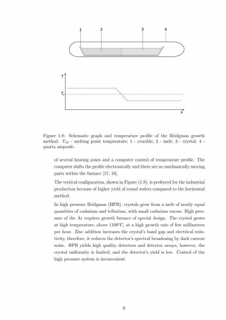
T
x
1 2 3 4
TM
Figure 1.8: Schematic graph and temperature profile of the Bridgman growthmethod. TM - melting point temperature; 1 - crucible; 2 - melt; 3 - crystal; 4 -quartz ampoule.
of several heating zones and a computer control of temperature profile. The
computer shifts the profile electronically and there are no mechanically moving
parts within the furnace [17, 18].
The vertical configuration, shown in Figure (1.9), is preferred for the industrial
production because of higher yield of round wafers compared to the horizontal
method.
In high pressure Bridgman (HPB), crystals grow from a melt of nearly equal
quantities of cadmium and tellurium, with small cadmium excess. High pres-
sure of the Ar requires growth furnace of special design. The crystal grows
at high temperature, above 1100C, at a high growth rate of few millimetres
per hour. Zinc addition increases the crystal’s band gap and electrical resis-
tivity, therefore, it reduces the detector’s spectral broadening by dark current
noise. HPB yields high quality detectors and detector arrays, however, the
crystal uniformity is limited, and the detector’s yield is low. Control of the
high pressure system is inconvenient.
9

1
2
3
x
TTM
Figure 1.9: Schematic graph and temperature profile of the vertical Bridgmangrowth method modification. TM - melting point temperature; 1 - quartz ampoule;2 - melt; 3 - crystal.
1.4 Defects
At the absolute zero temperature the crystal in the thermodynamic equilibrium is
completely ordered. This follows from the Gibbs free energy
∆G = ∆H − T∆S. (1.7)
At temperatures above absolute zero a deviation from ideal structure occurs. It can
be described in terms of different type defects. Electrical properties of the semicon-
ductor material greatly depend on the concentration of the point defects. Interaction
between defects is described by the quasi-chemical defect reaction (QCDR) approach
proposed by Kroger [19].
Electric properties at room temperature are influenced by defect reactions, which
proceed during the cooling, due to different electric characteristics (valence, ioniza-
tion energies) of the input/output reacting defects. The final defect structure is
determined by the temperature T at which the reactions have frozen. Generally
speaking, various defect reactions freeze at different temperatures and the final de-
fect structure is influenced by the whole history of the crystal.
Dominant native defects routinely accepted in CdTe are Cd vacancy (VCd), Cd
interstitial (CdI) and Te antisite (TeCd) [20, 21]. The existence of TeCd is well-
grounded in Te-rich CdTe [20, 21] but its electrical character has not been set yet.
10
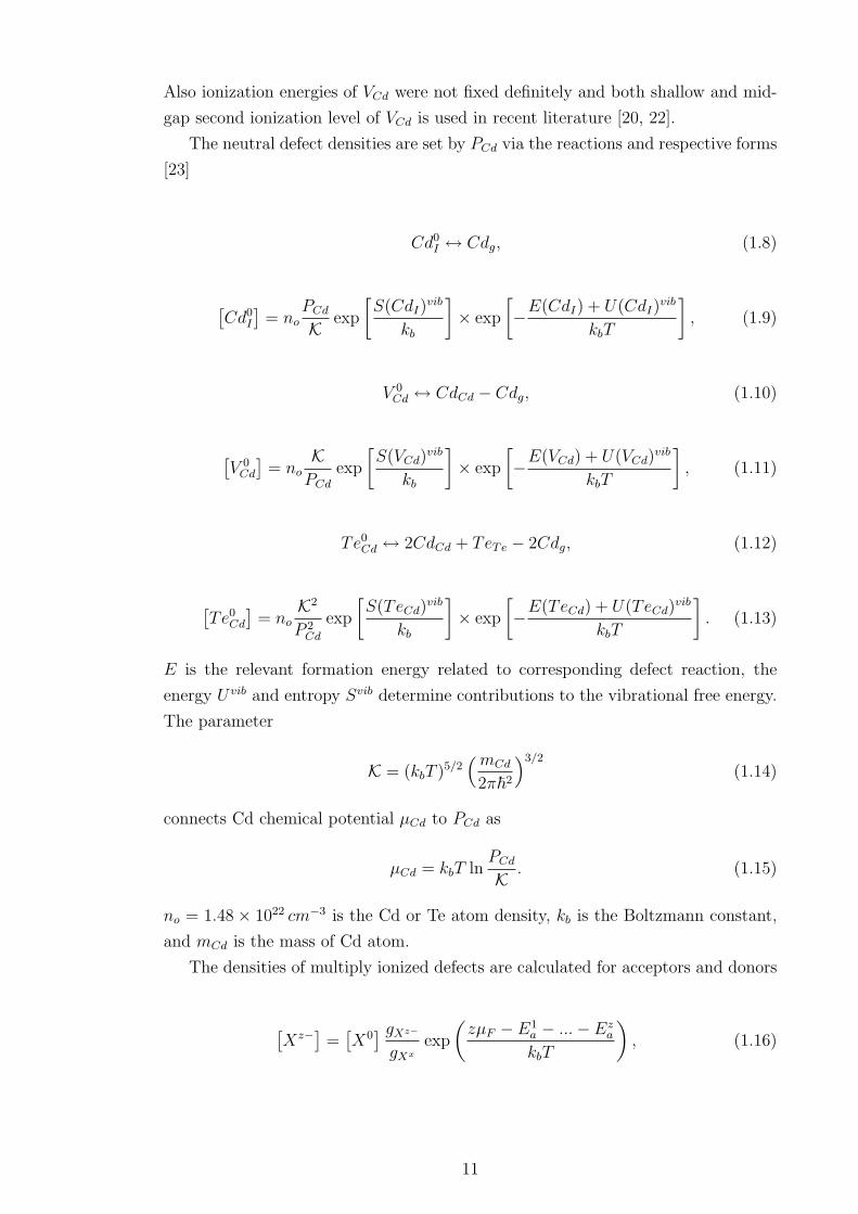
Also ionization energies of VCd were not fixed definitely and both shallow and mid-
gap second ionization level of VCd is used in recent literature [20, 22].
The neutral defect densities are set by PCd via the reactions and respective forms
[23]
Cd0I ↔ Cdg, (1.8)
[Cd0
I
]= no
PCd
Kexp
[S(CdI)
vib
kb
]× exp
[−E(CdI) + U(CdI)
vib
kbT
], (1.9)
V 0Cd ↔ CdCd − Cdg, (1.10)
[V 0
Cd
]= no
KPCd
exp
[S(VCd)
vib
kb
]× exp
[−E(VCd) + U(VCd)
vib
kbT
], (1.11)
Te0Cd ↔ 2CdCd + TeTe − 2Cdg, (1.12)
[Te0
Cd
]= no
K2
P 2Cd
exp
[S(TeCd)
vib
kb
]× exp
[−E(TeCd) + U(TeCd)
vib
kbT
]. (1.13)
E is the relevant formation energy related to corresponding defect reaction, the
energy U vib and entropy Svib determine contributions to the vibrational free energy.
The parameter
K = (kbT )5/2(mCd
2π~2
)3/2
(1.14)
connects Cd chemical potential µCd to PCd as
µCd = kbT lnPCd
K. (1.15)
no = 1.48× 1022 cm−3 is the Cd or Te atom density, kb is the Boltzmann constant,
and mCd is the mass of Cd atom.
The densities of multiply ionized defects are calculated for acceptors and donors
[Xz−] =
[X0] gXz−
gXx
exp
(zµF − E1
a − ...− Eza
kbT
), (1.16)
11

[Xz+
]=[X0] gXz+
gX0
exp
(E1
d + ... + Ezd − zµF
kbT
), (1.17)
where Ea and Ed are the acceptor and donor one-electron ionization energies. gXz−
and gXz+ are the degeneracies of the defects. The index z means the ionization
degree.
In Cl-doped CdTe the set of point defects is completed by shallow donor ClTe
and shallow acceptor complex labelled A-centre A≡(ClTeVCd). All defect densities
both in neutral and charged modifications are easily calculated with quasi-chemical
formalism [5]. In relatively strongly doped CdTe:Cl the Fermi energy µF is elevated
above the value in undoped CdTe and the density of native donors is reduced. At
PCd near saturation, the equilibrium density of TeCd is minimum and we thus omit
this defect in this thesis. In analytical calculations we skip also CdI and demonstrate
on exact numerical results the validity of such simplification.
The native defects formation, vibration, and ionization energies, vibration en-
tropies, factors of degeneracy as well as gap energy Eg according to [5] are used. The
second ionization energy of VCd is set 0.3Eg above the top of the valence band. The
density of Cl related A-centre formed by singly ionized V−Cd and Cl+Te is calculated
with
[A0]
=gA
no
[V−Cd
] [Cl+Te
]e− EA
kbT , (1.18)
[A−]
=[A0]
2e
µF−EakbT , (1.19)
where configuration degeneracy for A-center incorporating donor in Te sublattice
gA = 4, atom density of Cd or Te no = 1.48 × 1022 cm−3, and the A-centre ion-
ization energy Ea = 120 meV [24]. EA is the A-centre formation energy fitted to
experimental data.
Having fixed defect thermodynamic parameters, the Fermi energy is calculated
solving electric neutrality condition
n +[V−Cd
]+ 2
[V2−
Cd
]+[A−]
= (1.20)
p +[Cd+
I
]+ 2
[Cd2+
I
]+[Cl+Te
],
n, p being free electron and hole densities, with parallel fulfilment of Cl balance
equation
[Cl] =[Cl0Te
]+[Cl+Te
]+[A0]+[A−]. (1.21)
Leaving out defects with low density V−Cd, Cd+I , Cd2+
I , Cl0Te, A0, and p in eqs.
12

(1.20) and (1.21), n may be expressed as
n = [Cl]1− gA
2no
[V−Cd
]e
µF−Ea−EAkbT
1 + gA
2no
[V−Cd
]e
µF−Ea−EAkbT
− 2[V2−
Cd
]. (1.22)
Note that V−Cd cannot be neglected here due to multiplication with adjacent ex-
ponential function. Looking for the solution of equation (1.22), two characteristic
regimes are identified in CdTe:Cl. (i) At high PCd an uncompensated material char-
acterized by [VCd] [Cl] and stable n ≈ [Cl] is obtained. (ii) Lower PCd results in
an increased [VCd] and mutual donor-acceptor compensation, which allows to ne-
glect n in equation (1.22). Such a simplification immediately allows to establish the
correlation between µF and PCd in a form
µF ∝kbT
2ln PCd, (1.23)
which yields n ∝ P 0.5Cd being typical for compensated CdTe [25]. The relation (1.23)
implies that densities of principal point defects V2−Cd, A−, and Cd2+
I are only weakly
dependent on PCd in compensated regime.
1.5 Electric transport properties
The transport properties provide valuable information about the type and concen-
tration of the carriers, the band structure and the electron scattering mechanisms.
Transport properties of electrons and holes in cadmium telluride are influenced
by the scattering on the optical [26] and acoustic [27, 28] phonons and ionized
impurities. Since there are two atoms per primitive unit cell in zincblende structure,
there are six phonon branches - three acoustic and three optical. Along the high-
symmetry directions the phonons are classified as transverse or longitudinal. This
is done according to the displacement relatively to the direction of wave vector.
From the energy and temperature dependence of the scattering rate it can be
found, that:
• µ ≈ T−32 - scattering on acoustic phonons (deformation potential);
• µ ≈ T−12 - scattering on acoustic phonons (piezoelectric);
• µ ≈ T−12 - scattering on polar optical phonons;
• µ ≈ T32 - scattering on ionized impurities.
The combined mobility is given by the sum of different scattering mechanism
mobilities via Matthiessen rule
13

101
102
103
104
200 400 600 800 1000 1200 1400
Hal
l mob
ility
, cm
2 /Vs
T, K
Figure 1.10: Hall mobility data for electrons (O - Segall [29], - Turkevych [31], - Smith [32], N - Franc [33]) and holes (H - Yamada [30], - Turkevych [31], • -Smith [32]) in CdTe. Lines represents best theoretical fit for electrons [31] and holes[34]
µ =
(∑i
1
µi
)−1
. (1.24)
Experimental results on Hall mobility for electrons and holes are presented in
Figure (1.10). In case of electrons at lower temperatures the mobility is limited by a
scattering of electrons on ionized impurities and polar optical phonons [29]. At mid-
temperature region the scattering on polar optical phonons dominates. Theoretical
form for the polar optical phonon mobility of holes was proposed by Yamada [30]
µPOh = 57[e
252T − 1]. (1.25)
Recent results obtained at high temperatures are in good agreement with this model.
This means that no other type of scattering takes place there.
1.6 Application
CdTe and CdZnTe are used for various applications. CdTe is a highly useful material
in the making of thin film photovoltaic modules (photovoltaics). Thin-film CdTe
provides a greatly cost-effective solar cell design, but at a smaller efficiency than
poly-silicon.
CdTe can be alloyed with mercury to make a versatile infra-red detector material
(HgCdTe).
14

CdTe is used as an infra-red optical material for optical windows and lenses but
it has small application and is limited by its toxicity so that few optical laboratories
will consider working with it.
CdTe is also applied for electro-optical modulators. It has the greatest electro-
optic coefficient of the linear electro-optic effect among II-VI compound crystals
(r41 = r52 = r63 = 6.8×10⁻¹² m/V ).
CdTe alloyed with a small amount of zinc makes an excellent solid-state X-
ray and gamma ray detector (CdZnTe). Radiation detectors using CdZnTe can
operate in direct-conversion (or photoconductive) mode at room temperature, un-
like some other materials, particularly germanium, which require liquid nitrogen
cooling. Their relative advantages include high sensitivity for x-rays and gamma-
rays, due to the high atomic numbers of Cd and Te, and better energy resolution
than scintillator detectors. CdZnTe can be formed into different shapes for differ-
ent radiation-detecting applications, and a variety of electrode geometries, such as
coplanar grids, have been developed to provide unipolar (electron-only) operation,
thereby improving energy resolution.
The material has a high electro-optic coefficient and transparency in the mid-
infra-red region, making it a good modulator material for infra-red lasers. The same
properties make it useful for detection of terahertz waves.
An additional use is as a substrate material for the epitaxial growth of mercury
cadmium telluride (HgCdTe), an infra-red detector material. Cd0.96Zn0.04Te is al-
most perfectly lattice matched to LWIR HgCdTe (80% Hg, 20% Cd). However, it
is difficult to grow large crystals of fixed composition.
15
Chapter 2
Diffusion in CdTe
X-ray and gamma ray detector application depends upon properties of CdTe that are
sensitive to native defect and impurity concentrations which, in turn, are influenced
by crystal growth as well as by post-growth annealing processes.
Rather impressive changes in properties are produced by slight change in sto-
ichiometry – often less than 10−5 atomic fraction. CdTe changes the carrier type
with slight shift in stoichiometry. In a practical sense, the rate of change of crystal
composition upon annealing is relevant to the processing of this material for device
application. Changes in composition are controlled by the interdiffusion coefficient,
D, which is related to the self-diffusion coefficients and the thermodynamic factor.
The self-diffusion coefficients are in turn related to the individual defect concen-
trations and mobilities. Thus, the dependence of self-diffusion coefficients upon
component pressure provides insight into the dominant native defects which exist in
CdTe.
There are two principal diffusion quantities of interest in describing component
diffusion, the self-diffusion coefficients, DCd and DTe and the interdiffusion coeffi-
cient, DCdTe. Since there are no concentration differences in true self-diffusion, Fick’s
law should be obeyed and an experimental profile should be ’normal’ in the sense
that it may be analytically represented by the appropriate solution to Fick’s law.
By contrast, the interdiffusion coefficient may vary with position since interdiffusion
occurs in the presence of concentration gradients. The interdiffusion coefficient is
related to the self-diffusion coefficients by the Darken equation [35],
DCdTe = (NTeDTCd + NCdD
TTe) ·
d ln aCd
d ln NCd
, (2.1)
where NCd and NTe are the mole fractions of Cd and Te, DTCd and DT
Te are the tracer
diffusion coefficients of Cd and Te, and aCd is the activity of cadmium. The term
(d ln aCd/. lnNCd) is named the thermodynamic factor. The value of the DCdTe is
expected to be much larger than the largest of the self-diffusion coefficients because
of the large values expected for the thermodynamic factor.
16
Point defect model for the evaluation of tracer diffusion coefficients was proposed
by Chern and Kroger [36]:
DTCd =
1
n0
∑XCd
fXCdDXCd
[XCd], (2.2)
DTTe =
1
n0
∑XTe
fXTeDXTe
[XTe], (2.3)
where fXCd, fXTe
are correlation coefficients and DXCd, DXTe
are the diffusion coef-
ficients of the cadmium XCd and tellurium XTe related defects respectively.
2.1 Interdiffusion
Out of all II-VI compounds, which can be prepared both n- and p-type without
doping, CdTe has the widest gap. The n- of p-type is obtained by annealing in Cd
or Te atmosphere, respectively. The early research of diffusion in CdTe was made
by De Nobel [11]. Annealing was done at high temperature at pressure PCd. Sam-
ples were quenched to room temperature. Measured n-type electrical conductivity
varied as P1/2Cd . Assumption was made that high temperature defect structure is
preserved during the quenching operation. A conclusion was made that a singly
ionized cadmium interstitial dominates the charge neutrality condition:
[Cd+i ] = n = KP
1/2Cd . (2.4)
In the more recent measurements [37, 38, 32, 39] at elevated temperatures con-
ductivity was found to vary as P1/3Cd . This time doubly ionized cadmium interstitial
is considered to rule the charge neutrality condition:
2[Cd2+i ] = n. (2.5)
Independence of the conductivity from PCd at high cadmium pressure was reported
for the undoped CdTe [38]. No simple defect model has been proposed to explain
both these results and the high temperature conductivity.
The chemical diffusion coefficient was measured by relating step-like changes
in cadmium pressure (PCd) to subsequent changes in conductivity. The following
temperature dependence of the DCdTe for the temperature range 600-800 C was
given by Zanio [40]:
DCdTe = 4 · e−1.15±0.1eV
kBT (cm2/s). (2.6)
Rud’ and Sanin performed similar type measurements in the temperature range
700-900 C [41]:
DCdTe = 1.03 · e−0.97eV
kBT (cm2/s). (2.7)
17

It was also reported that diffusion data for increasing and decreasing step-change
in PCd produce slightly different DCdTe. For ∆PCd > 0 a single exponential described
the transient of the electrical conductivity while at ∆PCd < 0 a more complex be-
haviour involving conductivity varying with time according to a sum of two expo-
nential functions.
Detailed interpretation of interdiffusion in cadmium telluride in terms of native
point defects have been given in [42] and [43]. Intrinsic defects such as cadmium
vacancies and cadmium interstitials were reported to be responsible for the DCdTe.
2.2 Cd diffusion
Preliminary studies indicate that Cd-tracer diffusion coefficient DCd increases with
increasing cadmium pressure, which was associated with interstitial diffusion mecha-
nism [11]. Similar dependence was reported for CdS [44] and for CdSe [45]. However,
in later studies [46] of the cadmium self-diffusion in CdTe over the temperature range
700-1000 C and at various cadmium pressures DCd was found to be independent
of pre-annealing treatment and also independent of Cd pressure. The temperature
dependence was represented by:
DCd = (1.26+1.07−0.72)e
−2.07±0.08eVkT (cm2/s) (2.8)
for the whole temperature range. An exchange mechanism, a ring mechanism and
a neutral associate of a cadmium vacancy and cadmium interstitial were suggested
as a possible explanations for the independence of DCd upon PCd.
Time required to establish a new uniform conductivity after a change in compo-
nent pressure was also studied. It was found to be ∼103 shorter than times necessary
to homogenize the radio-tracer composition. Rapid rate of equilibration of the elec-
tronic defects was explained by the generation of point defects internally, without
mass transport from the external vapour. The crystal interior was presumed to
sense the external pressure changes via dislocations and thereby cause point defect
generation [47]. A quantitative correlation between the rate of attainment of elec-
tronic equilibrium, an estimated dislocation diffusion coefficient and the dislocation
density was shown. However, Zanio [40] showed that there is no correlation between
the interdiffusion coefficient and the dislocation density in CdTe.
A large difference in the rate of attainment of electronic equilibrium and the
homogeneous distribution of the tracer was explained by expected difference in dif-
fusion behaviour with and without a concentration gradient. The rate of attainment
of electronic equilibrium for a step jump in component pressure depends upon the
chemical diffusion coefficient, since a gradient in concentration is initially established
by changing the external component pressure. The tracer self-diffusion coefficient,
however, refers to diffusion in the absence of a concentration gradient and may be
18

much smaller then the interdiffusion coefficient [48]. In the CdTe the interdiffusion
coefficient is related to the two self-diffusion coefficients and the thermodynamic
factor, as given in equation (2.1).
It was reported later [36], that DCd is practically independent of PCd and low
cadmium pressures, but at high cadmium pressures DCd slightly increases and ap-
proaches DCd ∝ P1/3Cd relation near Cd saturated conditions. This effect became
significant at temperatures higher than 800C while at 700C the increase is smaller.
DCd was also reported independent of PCd in [49], within experimental error, as
determined by the values at PmaxCd and Pmin
Cd :
DCd(PmaxCd ) = 326× e
−2.67eVkBT (cm2/s) (2.9)
DCd(PminCd ) = 15.8× e
−2.44eVkBT (cm2/s) (2.10)
The complex defect model was developed to describe the diffusion behaviour, which
involves more than one mechanism. In accordance with equation (2.1), the two
largest contributions to DCd were reported to be interstitial mechanism involving
Cd2+i at high pressures, which is dependent upon P
1/3Cd , and a pressure independent
ring mechanism involving neutral associate (VCdCdi)0.
2.3 Te diffusion
Tellurium diffusion coefficient DTe varies reciprocally to PCd at all temperatures
over most of the region of CdTe solid stability [36, 49, 47]. The only exception is
the high cadmium pressure region. In [47] pressure dependency of the DTe at 800
was described by:
DTe = 1.6× 10⁻¹⁴P−1Cd (cm2/s) (2.11)
This equation is in good agreement with the temperature dependencies of the DTe
reported by Borsenberger and Stevenson [49]:
DTe(PmaxTe2
) = 1.66× 10⁻⁴e−1.38eV
kBT (cm2/s), (2.12)
DTe(PminTe2
) = 8.54× 10⁻⁷e−1.42eV
kBT (cm2/s). (2.13)
Pressure dependence was described by the relation:
DTe = DTe0iKi(T )P
1/2Te2
, (2.14)
where Ki is the mass action constant for the formation of Te0i .
Near cadmium saturated conditions the value of DTe becomes independent of
PCd. Another diffusion mechanism was proposed for this region [36]. Te diffusion
has contributions by tellurium interstitial Te−i and Te vacancy diffusion mechanisms.
19

From the equation (2.1) the dependence of the DTe from Cd vapour pressure can be
described:
DTe = DTe0iKTe0
iP−1
Cd + DV 2+Te
KV 2+Te
P1/3Cd , (2.15)
where DTe0i, DV 0
Terepresents the defects diffusivity and KTe0
i, KV 0
Terepresents the
mass action constants for the formation of tellurium interstitial, Te0i , and Te vacancy,
V 2+Te , defects respectively.
2.4 Chemical diffusion in CdTe:Cl
Given a concentration [Xq] of defect X with a charge q, the flux of Xq along the z
direction with the diffusion coefficient DqX is expressed by
JqX = −Dq
X
∂[Xq]
∂z+ < vq
X > [Xq]. (2.16)
The average velocity < vqX > is incurred by an internal electric field induced by
charged defects. Using the Nernst-Einstein relation and basic charge defect statis-
tics, JqX can be simplified to the form [50]
JqX = −Dq
X
[Xq]
[X0]
∂[X0]
∂z. (2.17)
The flux of the stoichiometry deviation ∆ is obtained as
J∆ =∑X,q
∂∆
∂[X0]Jq
X , (2.18)
where
∆ = [Cd]− [Te] =[Cd0
I
]+[Cd+
I
]+[Cd2+
I
]− (2.19)
−[V0
Cd
]−[V−Cd
]−[V2−
Cd
]+[Cl0Te
]+[Cl+Te
].
Chlorine A-centre does not appear in ∆ explicitly because it represents both one
Cd and one Te atoms missing in the lattice. Combining eqs. (2.17) and (2.18), the
chemical diffusion coefficient D is expressed in the form [51]
D = − J∆
∂∆/∂z=∑X,q
DqX
[Xq]
[X0]
∣∣∣∣d[X0]
d∆
∣∣∣∣ . (2.20)
To simplify the calculations, local defect equilibrium and quasi neutral approx-
imation are used as it is commonly done in such systems [50]. The diffusion of Cl
is not assumed. Consequently, all defect densities as well as µF may be expressed
with Cd chemical potential.
Usually, the diffusion flux is mediated by native vacancies and interstitials, for
20

that [X0] ∝ P±1Cd . Equation (2.20) can be than expressed in the form
D =
∑X,q Dq
X [Xq]
PCdd∆/dPCd
. (2.21)
In compensated CdTe:Cl with V 2−Cd dominant diffusing species, D is well approxi-
mated with
D =D(V2−
Cd
) [V 2−
Cd
]PCd
d([V 2−Cd ]−[Cl+Te]+n)
dPCd
≈D(V 2−
Cd
) [V 2−
Cd
]PCddn/dPCd
. (2.22)
Taking equation (1.23) into account, D ∝ P−0.5Cd is predicted for this case.
21

Chapter 3
Metal-semiconductor junction
Metal-to-semiconductor junctions are of great importance since they are present in
every semiconductor device. They can behave either as a Schottky barrier or as an
ohmic contact dependent on the character of the interface.
3.1 Energy band diagram
The barrier between the metal and the semiconductor can be identified on an en-
ergy band diagram. The energy band diagram of the metal and the semiconductor
aligned using the same vacuum level are shown in Figure 3.1. As the metal and
semiconductor are brought together, the Fermi energies of the metal and the semi-
conductor do not change right away. This yields the flatband diagram of Figure
3.2. The barrier height, φB, is defined as the potential difference between the Fermi
energy of the metal and the band edge where the majority carriers reside. As shown
in Figure 3.2, for an n-type semiconductor the barrier height is obtained from:
φB = Φm − χ. (3.1)
Φm is the work function of the metal and χ is the electron affinity of semiconductor.
The work function of selected metals as measured in vacuum can be found in Table
3.1. For p-type material, the barrier height is given by the difference between the
valence band edge and the Fermi energy in the metal:
φB =Eg
q+ χ− Φm (3.2)
A metal-semiconductor junction therefore forms a barrier for electrons and holes if
the Fermi energy of the metal as drawn on the flatband diagram is set between the
conduction and valence band edge.
The built-in potential, φI , is the difference between the Fermi energy of the metal
22
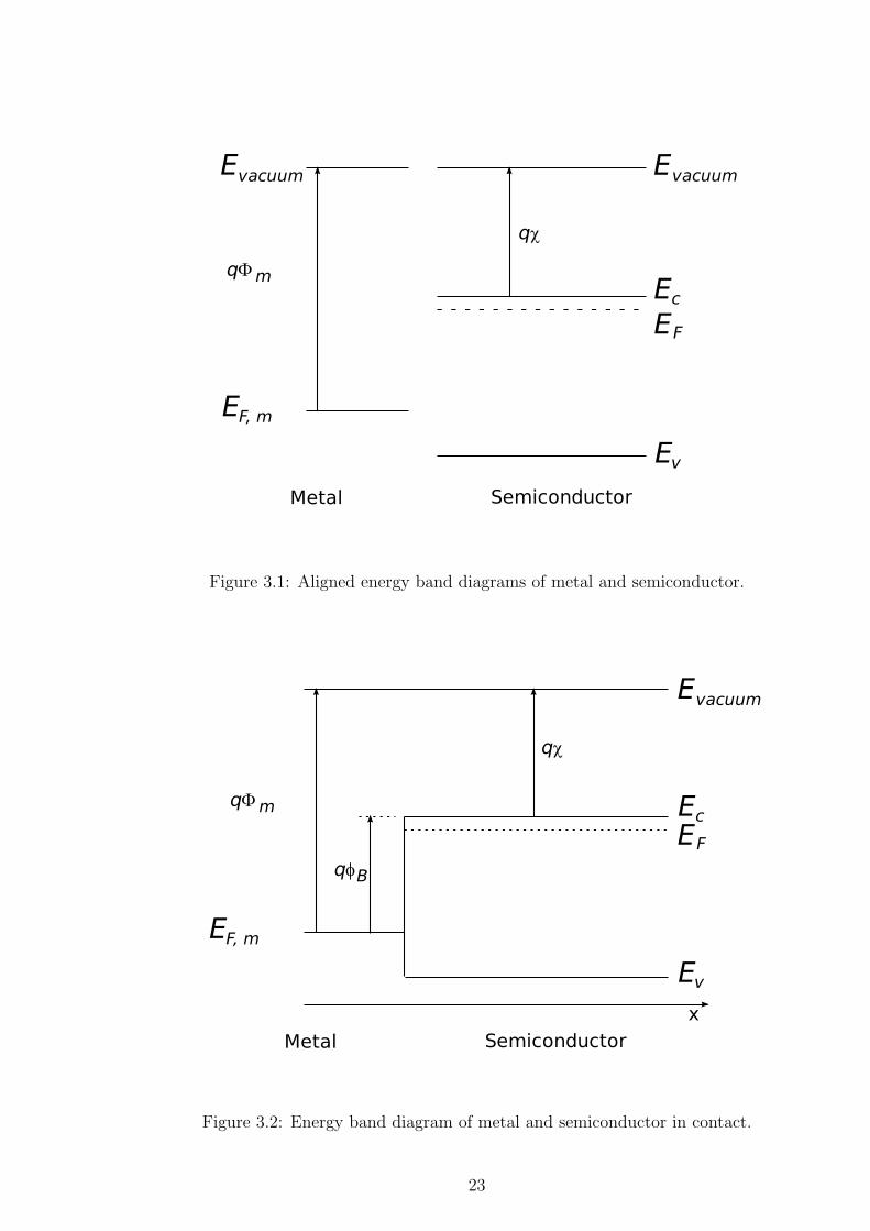
Evacuum
E
EE
EF, m
F
c
v
Evacuum
Metal Semiconductor
qm
q
Figure 3.1: Aligned energy band diagrams of metal and semiconductor.
Evacuum
EEF
c
Ev
qm
q
EF, m
Metal Semiconductor
qB
x
Figure 3.2: Energy band diagram of metal and semiconductor in contact.
23

Table 3.1: Work functions of selected metals [52]
Metal Crystallographic direction Work function φm, eV
Au 100 4.20110 4.06111 4.26
Pt polycrystalline 5.64110 5.84111 5.93320 5.22331 5.12
In polycrystalline 4.09
and that of the semiconductor and can be calculated from:
φI = Φm − χ− Ec − EF,n
q(3.3)
and
φI = χ +Ec − EF,p
q− Φm (3.4)
for n- and p-type semiconductor, respectively.
The measured barrier height for metal-semiconductor junctions often differs from
the ones calculated using (3.1) or (3.2). This is due to the complex behaviour of
the metal-semiconductor interface. The ideal metal-semiconductor theory assumes
that both materials are infinitely pure, that there is neither interaction between
the two materials nor an interface layer. Chemical reactions between the metal
and the semiconductor alter the barrier height as do interface states at the surface
of the semiconductor and interface layers. Some general trends however can still
be observed. As predicted by (3.1) and (3.2), the barrier height on n-type/p-type
semiconductor increases/decreases for metals with a higher work function.
3.2 Thermal equilibrium
The flatband diagram, shown in Figure 3.2, is not a thermal equilibrium diagram,
since the Fermi energy in the metal differs from that in the semiconductor. Electrons
in the n-type semiconductor can lower their energy by traversing the junction. As
electrons leave the semiconductor, a positive charge due to ionized donors stays
behind. This charge creates an electric field that lowers the band edges of the
semiconductor. Electrons flow into the metal until equilibrium is reached between
the diffusion of electrons from the semiconductor into the metal and the drift of
electrons caused by the field. This equilibrium is characterized by a constant Fermi
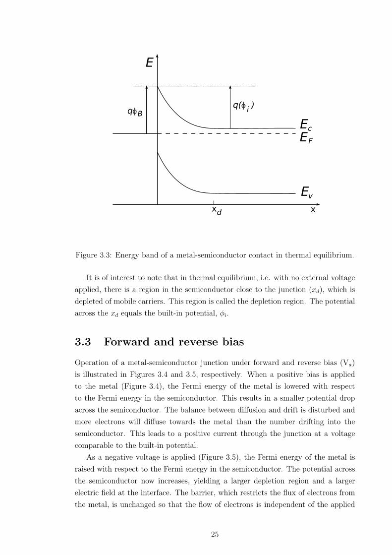
energy throughout the structure as shown in Figure 3.3.
24
qB
EEF
c
Ev
x
E
q( )i
xd
Figure 3.3: Energy band of a metal-semiconductor contact in thermal equilibrium.
It is of interest to note that in thermal equilibrium, i.e. with no external voltage
applied, there is a region in the semiconductor close to the junction (xd), which is
depleted of mobile carriers. This region is called the depletion region. The potential
across the xd equals the built-in potential, φi.
3.3 Forward and reverse bias
Operation of a metal-semiconductor junction under forward and reverse bias (Va)
is illustrated in Figures 3.4 and 3.5, respectively. When a positive bias is applied
to the metal (Figure 3.4), the Fermi energy of the metal is lowered with respect
to the Fermi energy in the semiconductor. This results in a smaller potential drop
across the semiconductor. The balance between diffusion and drift is disturbed and
more electrons will diffuse towards the metal than the number drifting into the
semiconductor. This leads to a positive current through the junction at a voltage
comparable to the built-in potential.
As a negative voltage is applied (Figure 3.5), the Fermi energy of the metal is
raised with respect to the Fermi energy in the semiconductor. The potential across
the semiconductor now increases, yielding a larger depletion region and a larger
electric field at the interface. The barrier, which restricts the flux of electrons from
the metal, is unchanged so that the flow of electrons is independent of the applied
25

qB
x
EEF
c
E
Ev
q( - V )i a
qVa
Figure 3.4: Energy band diagram of metal-semiconductor junction under forwardbias.
qB
x
EEF
c
E
Ev
q( - V )i a
qVa
Figure 3.5: Energy band diagram of metal-semiconductor junction under reversebias.
26

voltage. The metal-semiconductor junction with positive barrier height has therefore
a pronounced rectifying behaviour. A large current exists under forward bias, while
almost no current exists under reverse bias.
The potential across the semiconductor equals the built-in potential, φi, minus
the applied voltage, Va.
φ(x=∞) − φ(x=0) = φi − Va. (3.5)
3.4 Poisson equation
The electrostatic analysis of a metal-semiconductor junction is of interest since it
provides knowledge about the charge and field in the depletion region. It is also
required to obtain the capacitance-voltage characteristics of the contact.
For the general analysis Poisson equation is used:
d2φ
dx2= − ρ
εs
= − q
εs
(p− n + N+d −N−
a ) (3.6)
where, εs, is semiconductor permittivity, and the charge density, ρ, is written as
a function of the electron density, the hole density and the donor and acceptor
densities. To solve the equation, the electron and hole density, n and p, must be
expressed as a function of the potential, φ, yielding:
d2φ
dx2=
q
εs
[2ni · sinh(φ
Vt
) + N+d −N−
a ] (3.7)
with
φ =1
q(Ef − Ei), (3.8)
Vt =kT
q, (3.9)
n = nieφVt , (3.10)
p = nie− φ
Vt , (3.11)
where Ei is intrinsic Fermi energy, ni - intrinsic carrier density.
This second-order non-linear differential equation (3.7) can not be solved analyt-
ically. Instead, a simplifying assumption is usually made that the depletion region
is fully depleted and that the adjacent neutral regions contain no charge.
3.5 Full depletion approximation
The simple analytic model of the metal-semiconductor junction is based on the
full depletion approximation. This approximation is obtained by assuming that the
semiconductor is fully depleted over a distance xd, called the depletion region. While
27

this assumption does not provide an accurate charge distribution, it provides very
reasonable approximate expressions for the electric field and potential throughout
the semiconductor.
To apply the full depletion approximation to an M-S junction on n-type semi-
conductor, the depletion region is defined to be between the metal-semiconductor
interface (x = 0) and the edge of the depletion region (x = xd).
To find the depletion layer width, the electric field and the potential across
the semiconductor should be calculated as a function of the depletion layer width.
Requiring the potential across the semiconductor to equal the difference between
the built-in potential and the applied voltage, φi− Va, depletion layer width can be
found.
As the semiconductor is depleted of mobile carriers within the depletion region,
the charge density in that region is due to the ionized donors. Outside the depletion
region, the semiconductor is assumed neutral. This yields the following expressions
for the charge density, ρ:
ρ(x) = qNd, for 0 < x < xd (3.12)
ρ(x) = 0, for x ≥ xd (3.13)
where full ionization is assumed so that the ionized donor density equals the donor
density, Nd. This charge density is shown in Figure 3.6. The charge in the semicon-
ductor is exactly balanced by the charge in the metal, QM , so that no electric field
exists except around the metal-semiconductor interface.
Using Gauss’s law we obtain electric field as a function of position, also shown
in Figure 3.7:
ε(x) =qNd
εs
(xd − x), for 0 < x < xd (3.14)
ε(x) = 0, for x ≥ xd (3.15)
where εs is the dielectric constant of the semiconductor. The electric field is assumed
to be zero outside the depletion region. It is expected to be zero there since a non-
zero field would cause the mobile carriers to redistribute until there is no field. The
depletion region does not contain mobile carriers so that there can be an electric
field. The largest (absolute) value of the electric field is obtained at the interface
and is given by:
ε(0) = −qNdxd
εs
= −Qd
εs
(3.16)
where the electric field was also related to the total charge (per unit area), Qd, in
the depletion layer. Since the electric field is minus the gradient of the potential, one
obtains the potential by integrating the expression for the electric field, yielding:
φ(x) = 0, for x ≤ 0 (3.17)
28

xxd
qNd
Q = -QdM
Full depletionapproximation
actual
Q = qN xddd
Figure 3.6: Full depletion approximation charge density.
d
xx
Figure 3.7: Full depletion approximation electric field.
29
φ(x) =qNd
2εs
[x2d − (xd − x)2], for 0 < x < xd (3.18)
φ(x) =qNdx
2d
2εs
, for x > xd (3.19)
The potential across the metal can be neglected. Since the density of free carriers
is very high in a metal, the thickness of the charge layer in the metal is very thin.
Therefore, the potential across the metal is several orders of magnitude smaller than
that across the semiconductor, even though the total amount of charge is the same
in both regions.
The total potential difference across the semiconductor equals the built-in po-
tential, φi, in thermal equilibrium and is further reduced/increased by the applied
voltage when a positive/negative voltage is applied to the metal as described by
equation (3.5). This boundary condition provides the following relation between
the semiconductor potential at the surface, the applied voltage and the depletion
layer width:
φi − Va = −φ(x=∞) =qNdx
2d
2εs
. (3.20)
Solving this expression for the depletion layer width, xd, yields:
xd =
√2εs(φi − Va)
qNd
. (3.21)
3.6 Schottky diode current
The current across a metal-semiconductor junction is mainly due to majority car-
riers. Three distinctly different mechanisms exist: diffusion of carriers from the
semiconductor into the metal, thermionic emission of carriers across the Schottky
barrier and quantum-mechanical tunnelling through the barrier. The diffusion the-
ory assumes that the driving force is distributed over the length of the depletion
layer. The thermionic emission theory on the other hand postulates that only en-
ergetic carriers, those, which have an energy equal to or larger than the conduction
band energy at the metal-semiconductor interface, contribute to the current flow.
Quantum-mechanical tunnelling through the barrier takes the wave-nature of the
electrons into account, allowing them to penetrate through thin barriers. In a given
junction, a combination of all three mechanisms could exist. However, typically only
one mechanism limits the current, being denoted as the dominant current mecha-
nism.
3.6.1 Diffusion current
This model assumes that the depletion layer is large compared to the mean free
path, so that the concepts of drift and diffusion are valid. The resulting current
30

density equals:
Jn =qDnNc
Vt
√2q(φi − Va)Nd
εs
e−φB
Vt [eVaVt − 1] (3.22)
The current therefore depends exponentially on the applied voltage, Va, and the
barrier height, φB. The pre-factor can more easily be understood if one rewrites it
as a function of the electric field at the metal-semiconductor interface, εmax:
εmax =
√2q(φi − Va)Nd
εs
(3.23)
resulting:
Jn = qµnNcεmaxe−φB
Vt [eVaVt − 1] (3.24)
so that the pre-factor equals the drift current at the metal-semiconductor interface.
3.6.2 Thermionic emission
The thermionic emission theory assumes that electrons, which have an energy greater
than the top of the barrier, will cross the barrier provided they move towards the
barrier. The actual shape of the barrier is hereby ignored. The current density can
be expressed as:
Js→m = A∗T 2e−φB/Vt(eVa/Vt − 1) (3.25)
where A∗ = 4Rqm∗k2
h3 is the Richardson constant and φB is the Schottky barrier
height.
The expression for the current due to thermionic emission can also be written as
a function of the average velocity with which the electrons at the interface approach
the barrier. This velocity is referred to as the Richardson velocity given by:
νR =
√kT
2πm, (3.26)
so that the current density becomes:
Jn = qνRNce−φB
Vt [eVaVt − 1] (3.27)
This expression states that the current is the product of the electronic charge, q,
the velocity, ν, and the density of available carriers in the semiconductor located
next to the interface. The velocity equals the mobility multiplied with the field at
the interface for the diffusion current and the Richardson velocity for the thermionic
emission current. The minus one term ensures that the current is zero if no voltage
is applied as in thermal equilibrium any flux of carriers is balanced by a flux of
carriers in the opposite direction.
31

3.6.3 Tunnelling
The tunnelling current is obtained from the product of the carrier charge, velocity
and density. The velocity equals the Richardson velocity, the velocity with which
on average the carriers approach the barrier. The carrier density equals the density
of available electrons, n, multiplied with the tunnelling probability, Θ, yielding:
Jn = qνRnΘ, (3.28)
where νR is the Richardson velocity and n is the density of carriers in the semicon-
ductor. The tunnelling probability term, Θ, is obtained from:
Θ = e(− 43
√2qm∗~
φ3/2Bε
), (3.29)
and is added since the total current depends on the carrier flux arriving at the tunnel
barrier multiplied with the probability, Θ, that they tunnel through the barrier. The
tunnelling current therefore depends exponentially on the barrier height, φB, to the
3/2 power.
32

Chapter 4
Surface chemical treatment
Chemical etching is widely used on different stages of semiconductor device prepa-
ration [53, 54, 55]. Around 70 etching solutions, both selective and non-selective,
are currently used for surface treatment of CdTe and substitutional solid solution
alloys, mainly (CdZn)Te, based on it. Most of them were developed for the ele-
mentary and AIIIBV semiconductors. It was reported [56, 57, 58] that chemical
treatment strongly influences device electrical properties.
Etching solutions differ by the etching speed, roughness and stoichiometry of
obtained surface, contamination of the surface layer with solution components, etc.
Etching process is strongly influenced by various conditions like temperature
of the etching solution, speed of the etchant flux, previous surface treatment and
material purity.
One of the possible classification of etching solutions is by the power of oxidant.
4.1 Etching compositions with bromine
Bromine is one of the most frequently used oxidants in etching compositions for the
surface treatment of AIIBV I type semiconductor compounds [57]. It is because of:
• bromine is much softer oxidant than Cr+6 and H2O2 [53]
• bromides, obtained as a products of the oxidation process, are well soluble in
water
• oxidation products form a layer on the treated surface which allows to precisely
control reaction speed.
Solutions of elementary bromine in organic and inorganic solvents (methanol (CH3OH),
ethanol (C2H5OH), dimethylformamide ((CH3)2NC(O)H), hydrobromic acid (HBr))
are basically used for etching of AIIBV I type semiconductors. Bromine interacts
with the solvent, hence nature of the last one influences speed and character of the
surface treatment process.
33

The bromine concentration in solutions decreases gradually during preservation
even in a closed flask. pH of the solution decreases as well. Ethanol is oxidized by
the bromine:
C2H5OH + 2Br2 + H2O ↔ CH3COOH + 4HBr. (4.1)
Preservation of bromine-methanol solutions has the same problem.
As a result of surface treatment in bromine-methanol 0.5 % solution with il-
lumination sub-lattice limits are well defined on all planes for both CdTe and
Cd1−xZnxTe [59]. Etching in the same solution without illumination forms a big
concentration of cadmium vacancies (1− 4× 1014 cm−3) on the surface [60]:
CdTe + Br2(CH3OH) ↔ CdBr2(CH3OH) + Te, (4.2)
which can be removed electrochemically [61].
Tellurium layer formation on the CdTe surface after etching in 5 % Br-methanol
solution was experimentally determined by the Raman spectroscopy [62] and Auger
electron spectroscopy [63]. Layer thickness was found to be 1-4 nm. CdTe and
CdZnTe surface etched in 2 % bromine-methanol solution is also enriched with
tellurium [64, 65, 66]. Similar results are reported in [67, 68], where after two
minutes etching in 1 % bromine-methanol solution Cd/Te ratio is 0.43. Surface
treatment in 0.02 % Br2 solution in CH3OH forms 0.5-0.7 nm thick amorphous
tellurium layer [69, 70]. However, washing in NaBH4 decreases layer thickness to
0.25 nm. Maximum tellurium layer thickness is reported [67] to be as big as 40 A
depending on bromine concentration and etching time.
After 30 s, etching in bromine-methanol solution with 1 : 1 volume ratio a tel-
lurium dioxide was found on the CdTe surface along with tellurium. Cd/Te ratio
was 1.59. Heating in the vacuum to the 723 K helped to remove some amount of
TeO2 [60]. Etching CdTe in 10 % bromine-methanol solution forms on its surface
3−10 nm thick cadmium enriched layer (Cd/Te = 1.58). Tellurium is oxidized only
in the upper part of the layer (1−2 nm) and its composition is TeOx (x → 0). Thus,
after etching a heterostructure is formed on the CdTe surface. Roughly its structure
is: insulating layer (0.5 − 2 nm thick, Cd + TeOx + impurities), conductive layer
(6− 10 nm thick, Cd + Te), crystal volume [71].
In [72] layers formed on the CdTe surface after etching in 12 % bromine-methanol
solution were investigated by means of secondary mass-spectrometry (SIMS), Ruther-
ford back scattering and ellipsometry. It was found, that just etched surfaces are
slightly oxidized, enriched with Cd, Cd/Te ratio is 1.58. Surface layer thickness is
∼ 10 A, but in the atmosphere it increases with time. Increasing Te concentration
on the surface is explained by its diffusion from the sample volume.
34

Investigation of the CdTe surface etched in Br2-methanol and Br2-butanol showed,
that mainly cadmium is washed out as a result of Cd2+ and Br− interaction. When
the cadmium concentration reaches a critical value, structural changes occur, and
tellurium precipitates are formed. TeO2 is formed on such surface in water presence.
It is reported [73, 74], that 20 min. washing in methanol totally removes Br2
from the CdTe surface etched in 0.1 % bromine-ethanol solution, and Cd/Te ratio
decreases from 0.7 to 0.5. X-ray photoelectron spectroscopy (XPS) analysis showed
a presence of TeBr4 purely soluble in this solution. Bromine absorbed on the surface
can diffuse into the volume.
XPS results for the Cd0.2Hg0.8Te surface etched in 0.001 % Br2-CH3OH solution
are reported in [75]. Extremely small bromine concentration allows to etch with
the speed ∼ 0.1 nm/s. Chemical-mechanical polishing produce smooth surface with
surface composition close to that of the bulk material. The resultant surface can be
approximated as 0.8 nm Hg0.6Te/Hg0.8Cd0.2Te.
P-type CdTe surface composition after etching in some solutions containing
bromine were investigated by the XPS [76]. It was found, that 1 % bromine-methanol
solution gives Cd/Te = 0.7 ratio after 2 min. etching; 1 % Br2-CH3OH + 1M KOH
after 2 min treatment gives Cd/Te=0.67 ratio; 1 % bromine-methanol + hydrazine
after 2 min treatment with the following cleaning in the 0.5 N Na2S2O3 + 2M NaOH
in deionized water at 80− 90C gives Cd/Te=0.87 ratio; 1 % bromine-methanol +
hydrazine after 2 min treatment with the following cleaning in hydrazine (∼ 3 min)
gives Cd/Te=0.85 ratio. TeO2 layer was present after all treatments, since samples
were kept in the atmosphere.
CdTe surface preparation quality is critical for the device fabrication [77]. When
adding lactic acid to the bromine-methanol solution, the quality of x-ray and gamma
ray detectors improves [78]. After mechanical treatment with Al2O3 abrasive powder
(grain size 0.5 µm) and ultrasound cleaning in acetone, samples were etched in 5 %
bromine-methanol solution [79] or in 2 % Br2 in 20 % lactic acid solution in ethylene
glycol [80]. After the etching samples were cleaned in CH3OH. Etching speed of
n-type Cd1−xZnxTe (x = 0.1 - 0.2) in 2-10 % bromine solution in methanol was
50 µm/min at room temperature [81]. Etching time and removed layer thickness are
also very important parameters for the x-ray and gamma ray detector preparation
[82]. It was found that etching in bromine-ethylene glycol solutions for 6 min. is
optimal and significantly improves device properties.
4.2 Etching compositions with iodine
It is possible to use etching compositions containing iodine for the purpose of pol-
ishing and etching of the CdTe surfaces.
Surface treatment of the Cd1−xZnxTe was studied in detail in [83]. It was per-
35

formed in the aqueous solution containing 0.2 % I2 and 4 % NaI at room temperature.
Etching quality was judged by the surface look. XPS measurements were done to
define surface composition. Cd/Te ratio was found to be 0.36 which shows that
surface layer is significantly tellurium enriched.
It is generally known that polishing quality of the solution increases with the
increase of its viscosity. In order to obtain good quality polished surfaces of the
CdxHg1−xTe ethylene glycol was added to the etching solution [84]. It was shown
that treatment in I2-KI aqueous solution with ethylene glycol gives high quality
CdxHg1−xTe surface. Detailed study of the etching process for the CdTe, HgTe,
CdxHg1−xTe surfaces in the I2-KI-HBr aqueous solutions was done in [85, 86, 87].
Presence of ethylene glycol in the solution gradually decreases etching speed. Etch-
ing speed is also proportional to the iodine concentration [86]. This allows to control
etching process precisely.
Cd1−xZnxTe surface etching can be made in solution containing KIO3 [88]. Solu-
tion also contained lactic acid to decrease pH and increase chemical reaction speed.
XPS analysis showed smaller deviation from the stoichiometry in comparison with
using bromine-methanol solutions.
Adding organic acids into the etching solutions increases polishing effect. In order
to modify solution properties various acids (lactic C3H6O3, tartaric C4H6O6, citric
C6H8O7) were added to the H2O2-HI system [89]. Direct reaction speed dependence
on the acid concentration was confirmed.
4.3 Etching compositions with nitric acid
Nitric acid is used in etching compositions for the CdTe and in combination with
CrO3, K2Cr2O7, H2SO4. HNO3 acts as oxidant. Redox process has few stages [90]:
HNO2 + HNO3 ↔ 2NO2 + H2O, (4.3)
NO2 + e− ↔ NO−2 , (4.4)
NO−2 + H+ ↔ HNO2. (4.5)
HNO3 redox reaction is auto-catalytic, hence equations (4.3)-(4.5) correspond to
the equilibrium state where needed HNO2 concentration is already present in the
solution [91, 92]. Despite of good solubility of all etching reaction products, HNO3
is considered [91] to be not the best oxidant because of auto-catalytic character of
the process and huge nitrogen oxide gas emission.
Nitric acid forms on the CdxHg1−xTe thin layer of mercury compounds and can
be used for the Te layer removal formed after etching in bromine-methanol solution.
After 2 min. treatment in HNO3 tellurium layer was found on the surface [93]. Layer
thickness was reported to be ∼ 50 nm. Since the crystal structure of Te is different
36
from that of CdTe, the action of acid is not simply a ”leaching” of Cd atoms, leaving
a Te matrix. Instead, there is apparently a recrystallization, or epitaxy, from the
liquid [93].
XPS measurement shows a formation of the layer consisting of TeO2 and Te
after washing in concentrated HNO3 [94]. Auger electron spectroscopy and XPS
measurements did not show cadmium presence in the surface layer after etching in
15 % nitric acid [95]. Te layer thickness was estimated to be 60-80 nm [96].
Surface layer on the p-type CdTe has about 100 times smaller resistivity than the
volume and its thickness reaches 500 nm [97]. Etching in the solutions containing
HNO3 + H3PO4 + H2O leads to the surface enrichment with tellurium and increasing
solar cell sensitivity (∼12.5 %) on the structures CdTe-Sb/Au, which is much better
than after treatment in bromine-methanol solution [73].
To visualize structure defects in the semiconductor single-crystals (dislocations,
twins, point defects, inclusions, etc.) selective etching is used. It is based on etching
speed variation for different crystallographic directions.
In [98] dislocations were detected by chemical etching. Before etching samples
were mechanically polished by 1 µm Cr2O3 and chemically polished in 1 % bromine-
methanol solution, dissolving more than 20 µm to remove the damaged layer. After
that the samples were etched in the solution: 60 vol.part H2O, 1 vol.part Cr-acid,
1 vol.part concentrated HNO3, 1 vol.part concentrated HF. The etch pits produced
by the etchant were proven to be due to dislocations by correlating to each pit
patterns with X-ray reflection topography and by deformation experiments.
Etching with chromic acid (Na2Cr2O7 in 3M HNO3) increases the open-circuit
photovoltage as observed on the polished but not etched crystal, and increases the
short-circuit photocurrent density. It also reduces the surface defect concentration
as recorded by two-beam photocurrent spectroscopy [99].
In [100] one of the most widely used polishing etching solutions for cadmium
telluride was proposed - solution E (20ml HNO3 + 10ml H2O + 4g K2Cr2O7).
Mechanism for the CdTe etching in E solution is proposed in [101, 102]: NO−2
interacts mainly with Cd, Cr2O2−7 oxidises Te to insoluble TeO2, which is oxidized
by nitric acid to a soluble compounds. After treatment in E solution some amount
of chromium is reported to remain on the surface [103]. Cd/Te ratio in the surface
layer is 0.08 [96], layer thickness is 30− 60 nm. From the XPS measurements [104]
results the concentration peaks ratio Te/Cd > 9, and tellurium in the surface layer
is in oxidation state Te+4. After etching in this solution it is possible to define (111)
crystallographic direction on n-type CdTe by the etching pits [105, 106] and Cd and
Te sub-latices surfaces.
It is reported [107] that surface layer formed by etching in E solution consists of
Te and TeO2 and can gradually debase optical properties of the CdTe based devices.
37

4.4 Etching compositions with hydrogen peroxide
Because of strong oxidizing properties hydrogen peroxide (H2O2) is used for CdTe
etching only in a mixture with strong complex-forming agents, such as HF. Usage
of HF is motivated by the stability of 30 % H2O2 solution in such mixtures.
Cadmium telluride surface treated in solution 2 vol.part H2O2 + 3 vol.part HF
+ 1 vol.part H2O has 60-80 nm thick tellurium enriched surface (Cd/Te=0.2) [96].
Etching solution 2 vol.part H2O2 + 3 vol.part HF + 1 vol.part H2O is used for
the (111) CdTe surface identification and dislocation density study [108, 59]. After
etching of single-crystals Cd0.96Zn0.04Te in the solution with composition 200ml HF
+ 400 ml H2O2 + 400 ml H2O, grown steps were found on the surface (110) [109].
Surface layer formed by etching in solutions containing H2O2 were analysed by
the non-destructive spectroscopic ellipsometry [69]. It was found, that oxide layer
is not a mechanical mixture of CdO and TeO2, but a chemical compound, possibly
CdTeO3 or Cd2TeO5. It was established, that products solubility greatly depends
on solution pH, thus it is possible to control layer composition by changing pH.
SIMS analyses showed TeO, TeO2 and TeO3 presence in significant amount on
the surface etched in heated solution with composition 4 vol.part H2O2 + 1 vol.part
NH4OH [72]. Presence of TeO3 peak is explained by its forming from more complex
compounds like CdTeO3. Layer thickness is estimated to be 70-80 nm, and its
refraction index is ∼2 (close to that of TeO2). Additional oxidizing does not increase
thickness, but changes refraction index to 2.2.
Solution with composition 1 vol.part HF + 1 vol.part H2O2 + 1 vol.part CH3OH
was used to identify twins, inclusions and dislocation on CdTe surface [66].
4.5 Etching compositions with bases
For the preparation of the photovoltaic devices based on CdTe an etching in bases is
used. This process removes tellurium oxides layer formed during etching in solutions
with acids. It is known that at pH = 14 elementary chalcogens react by the following
equation:
4X + O2 + 8OH− ↔ 2XO2−3 + 4H2O + 2X2− (4.6)
It is reported [60], that at pH = 14 tellurium is reducted:
Te0 + e− ↔ 1/2Te2−2 . (4.7)
This process goes only if electric field is applied. Only electrochemical reduction
allows to remove peaks caused by tellurium layer presence. Simple etching in NaOH
solution does not help to remove surface film. Electrochemical reduction of CdTe in
1M KOH besides removing tellurium layer decreases cadmium vacancies concentra-
tion. Auger spectroscopy shows that 0.7 nm thick surface layer on the CdTe surface
38

after reduction in Na2SO4 + NaOH is enriched by cadmium (Cd/Te=1.42) [95].
Etching speed in this solution is 1.2 µm/min [96].
It should be mentioned, that in basic solution the surface oxidation can occur as
well. In order to obtain TeO2/CdxHg1−xTe heterostructure it was recommended to
oxidise plate surfaces in mixture of K2Fe(CN)6 and KOH.
39

Chapter 5
Experiment
5.1 Crystal growth
CdTe crystals were grown in our laboratory, in the Institute of Physics of Charles
University (Prague, Czech Republic). Growth was performed by a two-step method.
Initially polycrystalline CdTe was synthesized from component materials and doping
element. After that it was melted and recrystallized into single-crystalline ingot.
Synthesis of the material
Cadmium and tellurium for crystal preparation were commercially purchased (Nip-
pon Mining & Metals Co., Ltd., Japan). Materials purity was 6N (Table 5.1). Mate-
rials were loaded into the quartz ampoule in equiatomic relation. Walls of ampoule
were graphite covered to prevent crystal contamination. Ampoule was evacuated
out to the vacuum level better than 10−3 Pa and sealed. It was encapsulated in the
ampoule with bigger diameter to prevent material oxidation in case of accidental
crash of the main ampoule.
For the synthesis a horizontal furnace with 40 cm long working zone with uniform
temperature was used. Synthesis process requires a special temperature scheduler
to prevent ampoule explosion. The major part of the mixed material interacts and
forms CdTe at 750C, but the synthesis starts at 450C when Te melts. Reaction
between cadmium and tellurium is exothermic. Thus, rapid temperature increase
may occur. This would result in a huge cadmium partial pressure and consequent
ampoule explosion. For this reason the temperature increase was restricted to the
0.5C/min.
Synthesized CdTe was molten and held in that state for 10 hours at temperature
1115C for homogenization. Melt was solidified at a cooling rate 0.1C/min down
to 1085C when all material becomes solid. After that the ampoule was cooled
down to the room temperature without temperature control. Obtained ingot was
extracted from the ampoule and used as a source for CdTe single crystal growth.
40
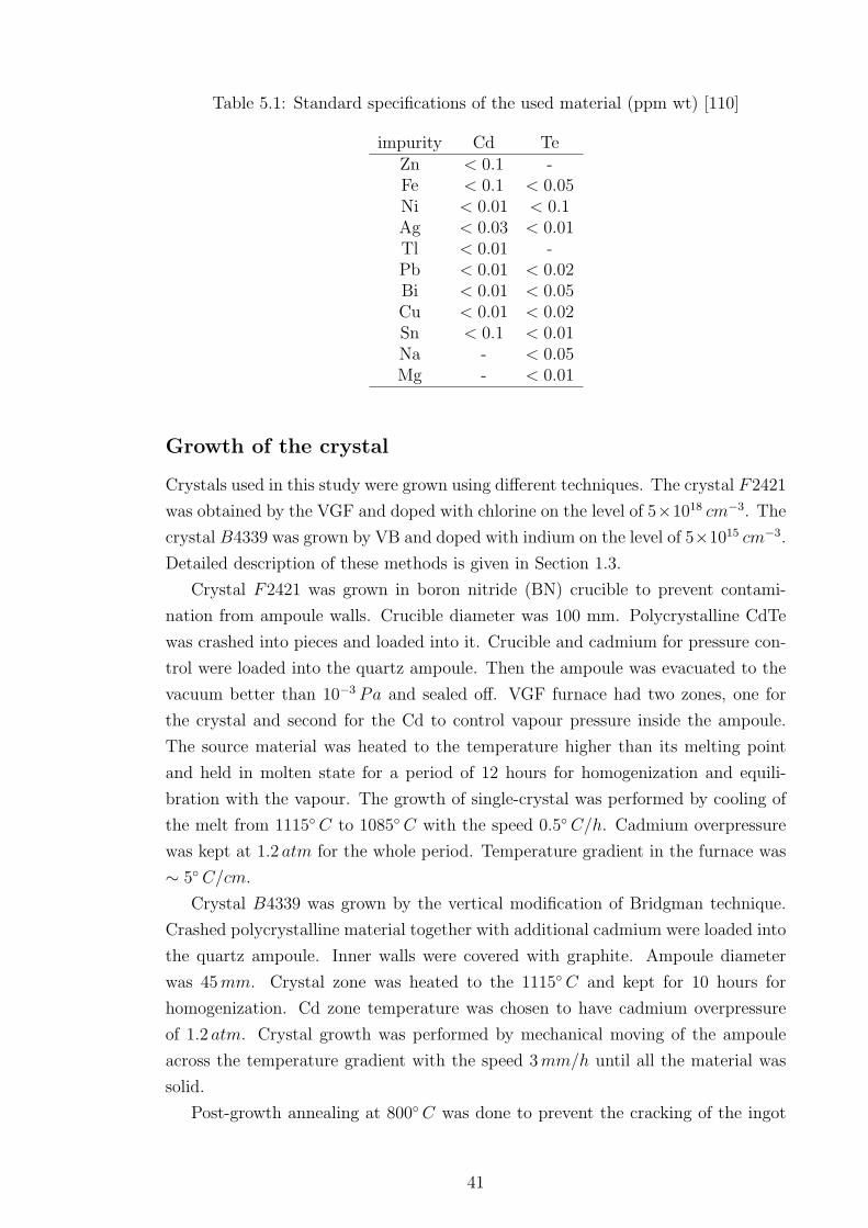
Table 5.1: Standard specifications of the used material (ppm wt) [110]
impurity Cd TeZn < 0.1 -Fe < 0.1 < 0.05Ni < 0.01 < 0.1Ag < 0.03 < 0.01Tl < 0.01 -Pb < 0.01 < 0.02Bi < 0.01 < 0.05Cu < 0.01 < 0.02Sn < 0.1 < 0.01Na - < 0.05Mg - < 0.01
Growth of the crystal
Crystals used in this study were grown using different techniques. The crystal F2421
was obtained by the VGF and doped with chlorine on the level of 5×1018 cm−3. The
crystal B4339 was grown by VB and doped with indium on the level of 5×1015 cm−3.
Detailed description of these methods is given in Section 1.3.
Crystal F2421 was grown in boron nitride (BN) crucible to prevent contami-
nation from ampoule walls. Crucible diameter was 100 mm. Polycrystalline CdTe
was crashed into pieces and loaded into it. Crucible and cadmium for pressure con-
trol were loaded into the quartz ampoule. Then the ampoule was evacuated to the
vacuum better than 10−3 Pa and sealed off. VGF furnace had two zones, one for
the crystal and second for the Cd to control vapour pressure inside the ampoule.
The source material was heated to the temperature higher than its melting point
and held in molten state for a period of 12 hours for homogenization and equili-
bration with the vapour. The growth of single-crystal was performed by cooling of
the melt from 1115C to 1085C with the speed 0.5C/h. Cadmium overpressure
was kept at 1.2 atm for the whole period. Temperature gradient in the furnace was
∼ 5C/cm.
Crystal B4339 was grown by the vertical modification of Bridgman technique.
Crashed polycrystalline material together with additional cadmium were loaded into
the quartz ampoule. Inner walls were covered with graphite. Ampoule diameter
was 45 mm. Crystal zone was heated to the 1115C and kept for 10 hours for
homogenization. Cd zone temperature was chosen to have cadmium overpressure
of 1.2 atm. Crystal growth was performed by mechanical moving of the ampoule
across the temperature gradient with the speed 3 mm/h until all the material was
solid.
Post-growth annealing at 800C was done to prevent the cracking of the ingot
41
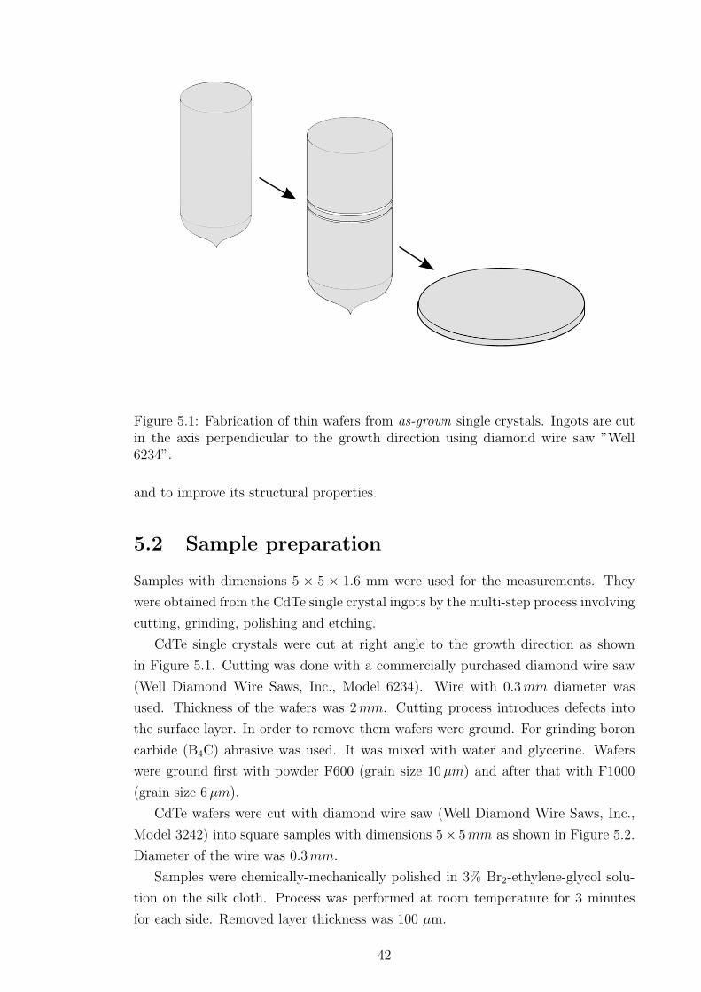
Figure 5.1: Fabrication of thin wafers from as-grown single crystals. Ingots are cutin the axis perpendicular to the growth direction using diamond wire saw ”Well6234”.
and to improve its structural properties.
5.2 Sample preparation
Samples with dimensions 5 × 5 × 1.6 mm were used for the measurements. They
were obtained from the CdTe single crystal ingots by the multi-step process involving
cutting, grinding, polishing and etching.
CdTe single crystals were cut at right angle to the growth direction as shown
in Figure 5.1. Cutting was done with a commercially purchased diamond wire saw
(Well Diamond Wire Saws, Inc., Model 6234). Wire with 0.3 mm diameter was
used. Thickness of the wafers was 2 mm. Cutting process introduces defects into
the surface layer. In order to remove them wafers were ground. For grinding boron
carbide (B4C) abrasive was used. It was mixed with water and glycerine. Wafers
were ground first with powder F600 (grain size 10 µm) and after that with F1000
(grain size 6 µm).
CdTe wafers were cut with diamond wire saw (Well Diamond Wire Saws, Inc.,
Model 3242) into square samples with dimensions 5× 5 mm as shown in Figure 5.2.
Diameter of the wire was 0.3 mm.
Samples were chemically-mechanically polished in 3% Br2-ethylene-glycol solu-
tion on the silk cloth. Process was performed at room temperature for 3 minutes
for each side. Removed layer thickness was 100 µm.
42

50 mm
5 m
m
5 mm
Figure 5.2: Preparation of samples. Wafers are cut on squares with diamond wiresaw ”Well 3242”.
Chemical etching in 3% Br2-methanol solution at room temperature for 1 minute
was the final step of the sample preparation. Measured thickness of the removed
layer was 14 µm.
After each process the surface was contaminated with different substances. In
case of cutting there were residues of CdTe itself, in grinding - abrasive powder, in
polishing and etching - products and reagents of the chemical reaction. Complex
washing was used to remove them. Washing was performed in distilled water, after
that in ethanol, next in acetone and finally samples were dried in the clean air flow.
5.3 Surface treatment
5.3.1 Etching techniques
Samples were chemically etched in various solutions to obtain surfaces with different
chemical composition, oxide thickness, roughness and electrical properties. Three
main solutions were: ”classical” bromine in methanol; solution emitting bromine
based on HBr and HNO3; and non-bromine solution with HI and hydrogen peroxide:
• Br - solution
Standard 3% solution of bromine in methanol.
Used at room temperature immediately after mixing
• HBr - solution
43

HNO3 + HBr + C4H6O6
Solution needed to be left for 2 hours after mixing. Used at room temperature
• HI - solution
H2O2 + HI + C6H8O7
Solution needed to be left for 2 hours after mixing. Used at room temperature.
Etching was performed using rotation equipment. Samples were submerged in
the solution and rotated with the speed 90 rotations per minute. Sample thickness
was checked before and after etching to define process speed. After the etching the
surface was cleaned in ethanol, acetone and distilled water. Finally, it was dried in
the flow of warm air.
5.3.2 Surface roughness study
The surface roughness of the samples was measured by means of a noncontact 3D
surface profiler (Zygo NewWiew 5000, USA), pictured in Figure 5.3. This micro-
scope uses noncontact scanning white-light interferometry to acquire ultrahigh Z-
resolution images. The measurement is based on the interferometry - a traditional
technique in which a pattern of bright and dark lines (fringes) results from an opti-
cal path difference between the reference and sample beams. Incoming light is split
inside an interferometer, one beam going to an internal reference surface and the
other to measured sample. After reflection, the beams recombine inside the device,
undergoing constructive and destructive interference and producing the light and
dark fringe pattern.
5.4 Contact preparation
Contacts are the important part of any detector device. Also they are needed to
make electrical measurements of the properties of material or metal-semiconductor
junction. The contact quality influences the precision of measurements.
Taking into the consideration differences of the performed experiments in every
particular case different contacts were prepared. First part of the research was
on high-temperature bulk material properties. Here we tried to prepare stable at
high temperature ohmic contacts, so they would not influence measured values.
In the second part the properties and preparation techniques of the contacts were
investigated. Here different contacts, both ohmic and rectifying, were made.
5.4.1 Welding wires for the high-temperature measurements
High-temperature measurements were done in the atmosphere of cadmium. Thus,
thermal stability and chemical passivity to the Cd vapour were required for the
44

Figure 5.3: Zygo NewWiew 5000 noncontact 3D surface profiler.
1
2
3
Figure 5.4: Molybdenum wires welded into the sample. 1 - sample; 2 - Mo wire; 3 -quartz capillary tube.
45

1
2
3
4
Figure 5.5: Contacts prepared by the chemical deposition or by the thermal evapo-ration. 1 - sample; 2 - deposited metal; 3 - silver paste or soldered indium; 4 - silverwire.
contacts. Molybdenum wires satisfy both requirements and therefore were used in
our study.
Mechanically pressed contacts are commonly used for the high-temperature mea-
surements [111]. However, the local sublimation of CdTe under the wire, especially
in case of low component overpressure, results in a lost of the electrical connection.
Therefore, welding of the wire into the sample was used.
Surface of the wires was cleaned prior to contact fabrication. For the cleaning
the boiling 15 % water solution of NaOCl was used. After 5 min cleaning the wires
were washed in water and then in methanol. The welding was done in an argon
atmosphere to prevent sample and contact oxidation. Each wire was bent after the
welding and put into the quartz capillary tube. No sample holder was needed since
Mo wire were hard enough to hold the sample inside the ampoule (Figure 5.4).
5.4.2 Chemical deposition of metals
Gold and platinum were chemically deposited to fabricate metal-semiconductor junc-
tions. Sample surfaces were masked with photoresist. Windows were left in places
where metallic contacts were desired to be formed. Samples were heated in oven to
80C for a period of 20 minutes for photoresist to harden.
Gold was deposited from the 5% water solution of chloroauric acid (HAuCl4).
46

Chemical reaction can be written as follows:
[AuCl4]− + 3e− → Au + 4Cl− (5.1)
Process was done at room temperature. Deposition time was 1 minute. Deposition of
platinum was similar. It was performed from 0.5% water solution of hexachloropla-
tinic acid (H2PtCl6). Solution was heated to 95C. Deposition time was 2 minutes.
Chemical reaction is:
[PtCl6]2− + 4e− → Pt + 6Cl− (5.2)
As a result, thin layer of metal was formed on the top of CdTe. Remaining photore-
sist was removed in the acetone. Samples were washed in distilled water, after that
in ethanol and in acetone. Finally it was dried in the flow of the warm air.
5.4.3 Thermal evaporation of metals
Thermal evaporation was used to deposit gold and indium contacts. Samples were
masked with photoresist in the same way as for the chemical deposition. Chamber
was evacuated to the vacuum better than 10−3 Pa. A thin layer of metal was de-
posited on the sample. After the deposition samples were washed and dried by the
same scheme as in the chemical deposition.
Silver wires were connected to the metallic contacts. Diameter of the wires was
0.05 mm. Contacting was done either by the silver paste or by the indium (Figure
5.5). It was found that soldering with In may change electrical properties of the
contacts. That is why silver paste was chosen to be main contacting substance and
indium was used for the comparison. When using silver, samples were left for 30 min
to harden the paste. No sample heating was used to prevent silver diffusion into the
volume.
5.5 Electrical measurements
Series of various electrical measurements were carried out to investigate both mate-
rial properties and contact preparation techniques.
Chemical self-diffusion in semi-insulating CdTe was studied indirectly through
the conductivity. Hall effect measurements were performed to define material main
properties. Contacts were characterized by the V-I curves obtained from the current-
voltage characteristic. Samples homogeneity was evaluated by the resistivity map-
ping.
47
5.5.1 Hall effect
Hall effect measurements were used, since they give a complex information about
semiconductor material properties including conductivity type, concentration of the
carriers and their mobility. The measured value was Hall voltage, which is given by
Uy =RHIxBz
b= RHjxBz, (5.3)
where b is a sample thickness in the direction of the magnetic field, RH is the Hall
coefficient and jx is the current density. The sign of the Hall coefficient allowed us
to define the conductivity type of the material. Its value is negative for n-type and
positive for p-type:
RH = −rH
nq, (5.4)
with rH , Hall factor, close to 1. Thus, the carrier concentration is determined as
n = − 1
RHq. (5.5)
The Hall mobility is defined by the product of the zero-field conductivity, σ0 and
the Hall coefficient:
µH = |RHσ0|. (5.6)
Van der Pauw method was used for the measurements. The circuit was the same,
as used for the study of the conductivity.
High-temperature Hall effect and conductivity measurements were performed in
a two-zone vertical furnace, which was fixed inside the magnet. Zone one, with the
sample, was located in the centre of the magnet coils. Zone two, with component,
was used to control component overpressure. Experimental set-up is shown in Figure
5.6. Temperature was controlled by the Eurotherm 2408 PID controllers. For the
measurement direct current and direct 0.5 T magnetic field were used. The wires
from the sample were connected to the switch system as shown in Figure 5.7.
5.5.2 Conductivity
Van der Pauw method was used for study of the conductivity. This method can be
used to measure specific resistivity and Hall effect on flat samples with an arbitrary
shape. This method allowed us to perform electrical measurements knowing only
one geometric parameter - sample thickness. Specific resistivity was calculated from
48
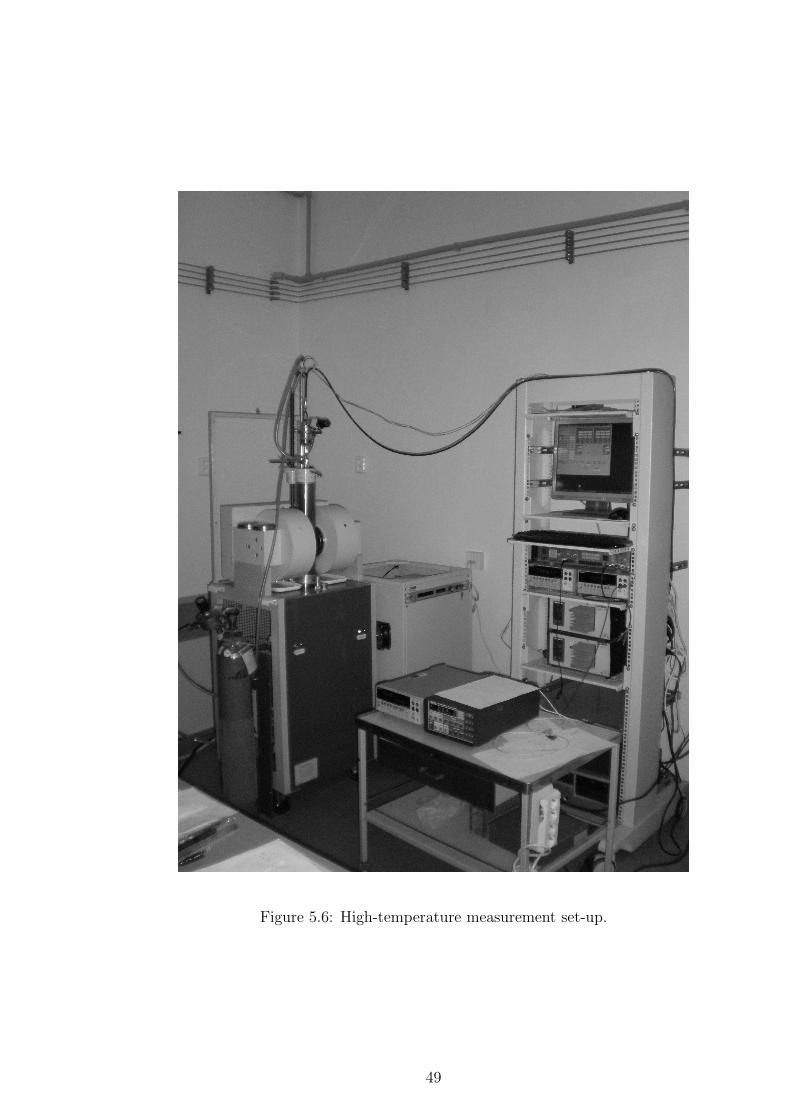
Figure 5.6: High-temperature measurement set-up.
49
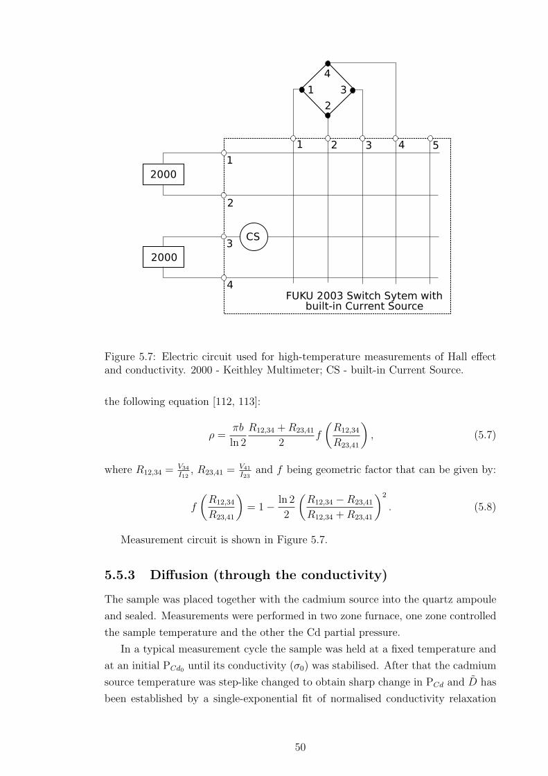
1
1
1
2
2
2
3
3
3
54
4
4
2000
2000
CS
FUKU 2003 Switch Sytem with built-in Current Source
Figure 5.7: Electric circuit used for high-temperature measurements of Hall effectand conductivity. 2000 - Keithley Multimeter; CS - built-in Current Source.
the following equation [112, 113]:
ρ =πb
ln 2
R12,34 + R23,41
2f
(R12,34
R23,41
), (5.7)
where R12,34 = V34
I12, R23,41 = V41
I23and f being geometric factor that can be given by:
f
(R12,34
R23,41
)= 1− ln 2
2
(R12,34 −R23,41
R12,34 + R23,41
)2
. (5.8)
Measurement circuit is shown in Figure 5.7.
5.5.3 Diffusion (through the conductivity)
The sample was placed together with the cadmium source into the quartz ampoule
and sealed. Measurements were performed in two zone furnace, one zone controlled
the sample temperature and the other the Cd partial pressure.
In a typical measurement cycle the sample was held at a fixed temperature and
at an initial PCd0 until its conductivity (σ0) was stabilised. After that the cadmium
source temperature was step-like changed to obtain sharp change in PCd and D has
been established by a single-exponential fit of normalised conductivity relaxation
50
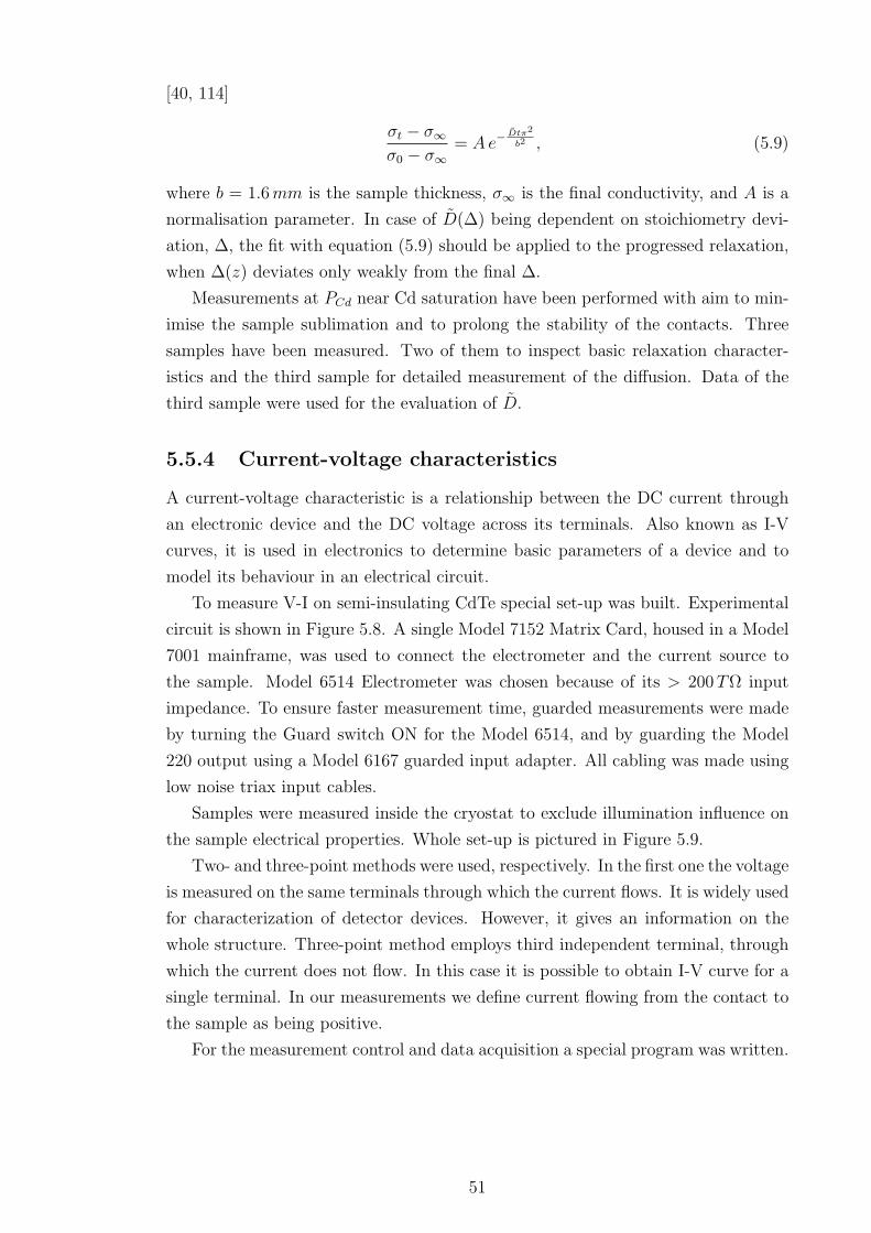
[40, 114]
σt − σ∞σ0 − σ∞
= A e−Dtπ2
b2 , (5.9)
where b = 1.6 mm is the sample thickness, σ∞ is the final conductivity, and A is a
normalisation parameter. In case of D(∆) being dependent on stoichiometry devi-
ation, ∆, the fit with equation (5.9) should be applied to the progressed relaxation,
when ∆(z) deviates only weakly from the final ∆.
Measurements at PCd near Cd saturation have been performed with aim to min-
imise the sample sublimation and to prolong the stability of the contacts. Three
samples have been measured. Two of them to inspect basic relaxation character-
istics and the third sample for detailed measurement of the diffusion. Data of the
third sample were used for the evaluation of D.
5.5.4 Current-voltage characteristics
A current-voltage characteristic is a relationship between the DC current through
an electronic device and the DC voltage across its terminals. Also known as I-V
curves, it is used in electronics to determine basic parameters of a device and to
model its behaviour in an electrical circuit.
To measure V-I on semi-insulating CdTe special set-up was built. Experimental
circuit is shown in Figure 5.8. A single Model 7152 Matrix Card, housed in a Model
7001 mainframe, was used to connect the electrometer and the current source to
the sample. Model 6514 Electrometer was chosen because of its > 200 TΩ input
impedance. To ensure faster measurement time, guarded measurements were made
by turning the Guard switch ON for the Model 6514, and by guarding the Model
220 output using a Model 6167 guarded input adapter. All cabling was made using
low noise triax input cables.
Samples were measured inside the cryostat to exclude illumination influence on
the sample electrical properties. Whole set-up is pictured in Figure 5.9.
Two- and three-point methods were used, respectively. In the first one the voltage
is measured on the same terminals through which the current flows. It is widely used
for characterization of detector devices. However, it gives an information on the
whole structure. Three-point method employs third independent terminal, through
which the current does not flow. In this case it is possible to obtain I-V curve for a
single terminal. In our measurements we define current flowing from the contact to
the sample as being positive.
For the measurement control and data acquisition a special program was written.
51
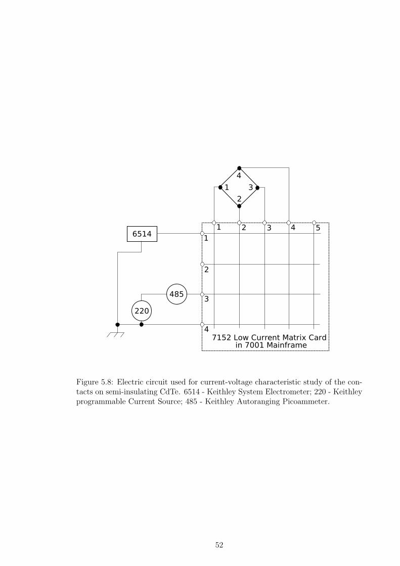
1
1
1
2
2
2
3
3
3
54
4
4
6514
485
7152 Low Current Matrix Card in 7001 Mainframe
220
Figure 5.8: Electric circuit used for current-voltage characteristic study of the con-tacts on semi-insulating CdTe. 6514 - Keithley System Electrometer; 220 - Keithleyprogrammable Current Source; 485 - Keithley Autoranging Picoammeter.
52
Figure 5.9: Low-temperature measurement set-up used for current-voltage charac-teristics study.
53

5.5.5 Capacitance-voltage
The capacitance per unit area of the Schottky diode is given by
C
A=
√±qεrε0(NA −ND)
2(±Vbi ± V − kTq
)(5.10)
where the ”+” sign applies to a p-type (NA > ND) and the ”-” sign to an n-type
(NA < ND) material, εr is semiconductor dielectric constant, and V is the reverse-
bias voltage [115]. For n-type material NA < ND, Vbi < 0, and V < 0, whereas
for p-type material NA > ND, Vbi > 0, and V > 0. The kTq
in the denominator
accounts for the majority carrier tail in the space-charge region which is omitted in
the depletion approximation. The built-in potential is related to the barrier height
by the relationship
φB = Vbi + V0 (5.11)
V0 = (kT
q) ln
Nc
ND
, (5.12)
where Nc is the effective density of states in the conduction band. Plotting 1/(CA)2
versus V gives a curve with slope 2/[qεrε0(NA−ND)], and with the intercept on the
V -axis, Vi = −Vbi + kTq
.
The barrier height is determined from the intercept voltage by
φB = −Vi + V0 +kT
q(5.13)
With aim to collect maximum information about measured samples, we have
utilized kind offer to exploit the equipment of the CNRL (VUT, Brno) and per-
formed capacitance-voltage measurements there. Agilent E4980A Precision LCR
Meter was chosen for its wide frequency range, powerful compensation functions,
and highly accurate bias characteristics. This versatility of the meter guaranteed
highly accurate C-V measurements, and higher efficiency in the evaluation of MOS
properties.
5.5.6 Resistivity mapping
Time Dependent Charge Measurements (TDCM) was utilized for the resistivity
mapping [116]. This contactless non destructive method allowed to study areal
homogeneity of the resistivity without degrading of the surface quality. In this
method the sample acts as a capacitor and the resistivity is evaluated by measuring
a time dependent charge transient observed after application of a voltage step.
The CdTe wafer was inserted between a 2.5 mm in diameter measurement elec-
trode, surrounded by an extended guard electrode, and a back electrode (Figure
54
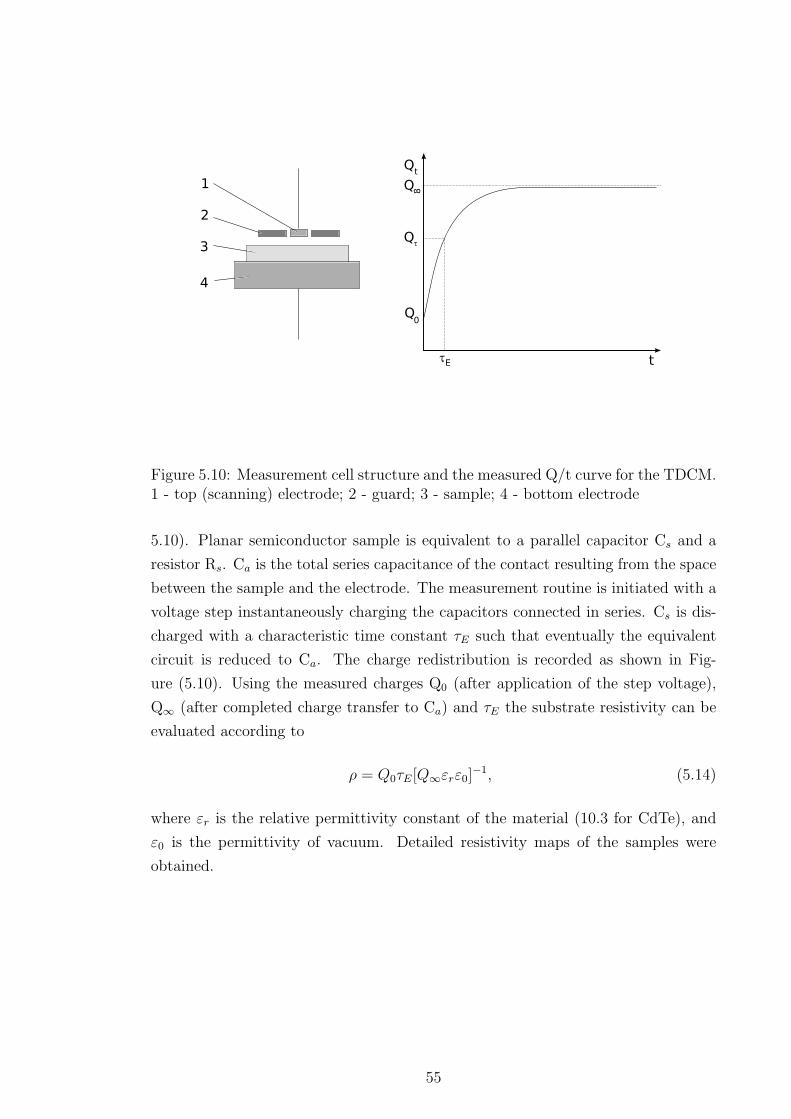
t
Q
Q
Q
Q
t
8
0
1
2
3
4
E
Figure 5.10: Measurement cell structure and the measured Q/t curve for the TDCM.1 - top (scanning) electrode; 2 - guard; 3 - sample; 4 - bottom electrode
5.10). Planar semiconductor sample is equivalent to a parallel capacitor Cs and a
resistor Rs. Ca is the total series capacitance of the contact resulting from the space
between the sample and the electrode. The measurement routine is initiated with a
voltage step instantaneously charging the capacitors connected in series. Cs is dis-
charged with a characteristic time constant τE such that eventually the equivalent
circuit is reduced to Ca. The charge redistribution is recorded as shown in Fig-
ure (5.10). Using the measured charges Q0 (after application of the step voltage),
Q∞ (after completed charge transfer to Ca) and τE the substrate resistivity can be
evaluated according to
ρ = Q0τE[Q∞εrε0]−1, (5.14)
where εr is the relative permittivity constant of the material (10.3 for CdTe), and
ε0 is the permittivity of vacuum. Detailed resistivity maps of the samples were
obtained.
55

Chapter 6
Results & Discussions
6.1 Sample characterization
All studied samples were cut from single crystals. However, it was taken into the
consideration that even inside one grain a gradient of material properties can be
observed. Such heterogeneity may be crucial for measurement precision and can
significantly decrease that. Thus, special measures were taken to eliminate possible
errors. Both volume and surface of the samples were controlled. Prior to electrical
measurements samples were mapped to define degree of their homogeneity. Also
surface topology was measured after treatment in various etching solutions.
6.1.1 Resistivity mapping
Resistivity mapping was done using commercially available equipment (COREMA,
SemiMap Scientific Instruments, Germany). The capacitive metal electrodes above
and below the sample were positioned by fast and precise xy translation. They
defined local sample and air capacitors at the desired measurement spot. A charging
voltage step was applied to the R-C circuit and the dynamic charge redistribution
was recorded. The resistivity was obtained from the initial and final charge values
and the relaxation time. A typical result obtained from measurement is shown in
Figure 6.1.
Distribution of the resistivity in all samples was similar. The electrical resistivity
of semi-insulating samples ranged from ∼ 3×10⁹ to 4.5×10⁹ Ωcm. Excluding edges,
waste area resistivity lies in the range from 3.3× 10⁹ to 3.5× 10⁹ Ωcm. Sample do
not have any grain boundaries. Resistivity is homogeneously distributed trough the
whole volume of the sample.
6.1.2 Surface topology
Topology was studied on surfaces treated in two different etching solutions (HBr
and HI). Samples were etched for 20, 40, and 60 seconds. One additional measure-
56

Figure 6.1: A typical image obtained from the sample resistivity mapping. Left partshows the areal resistivity profile, right part plots the resistivity distribution.
Table 6.1: Comparison of surface roughness after treatment in various solutions.
etching roughness, nmtime, s HBr - solution HI - solution
before etching 9.22 8.0620 5.20 5.3040 4.92 1.4560 3.08 1.53
57

ment was made before etching to be used as a reference. Results of the root-mean-
square roughness measurements are summarized in Table 6.1. Initial surfaces of the
samples just after polishing are similar. Roughness better than 10 nm is the best
quality which is possible to obtain on the hand-polished surfaces. By the chemical-
mechanical polishing smoother surface can be manufactured only by using precise
polishing equipment. Further improvement of the samples’ properties was made by
the chemical etching process. For the HBr-solution the lowest surface roughness
(the better quality) is obtained after 60 s. It is on the level of ∼ 3 nm. In case of
HI-solution the best quality is reached after 40 s. This time is enough to get even
better surface with twice lower roughness at the level under 1.5 nm. Etching rate for
this particular solution is different (HBr - 4.33 µm/min; HI - 15 µm/min). Thus,
to remove destructed layer in HBr-solution longer time is needed. Roughness of the
sample surface after etching in HI-solution for 60 s has slightly higher value. Since
the difference is within the statistical deviation it is considered irrelevant. These
results show that the etching process consists of at least 2 stages. On the first stage
surface inhomogeneities are removed faster. This can be explained by the nature
of the etching solution. None of the etchant is absolutely non-selective. At the
beginning of the etching process peaks are removed faster which results in obtaining
smoother surfaces. On the second stage after removing damaged layer and reaching
the best surface quality etching speed normalises for the whole surface area. How-
ever, in case of large stock removal, the surface roughness starts to increase since
etching process is very complex and is never homogeneous.
Three dimensional (3D) surface maps for the modular scanning areas of 0.18 mm×0.13 mm are presented in the Figures 6.2 and 6.3. They represent surfaces of the
CdTe samples treated at room temperature in HBr - solution for 60 s and in HI
- solution for 40 s respectively. Thin peaks on both figures correspond to settled
powdery dust. The deviations from the ideal flat surface in the form of waves is
caused by the crystal structure of the samples. Semiconductor crystals contain dif-
ferent kinds of defects as described in Section 1.4. Etching rate for these defects
differs from the perfect crystal lattice. As a result in places where defects came into
the the surface sample is etched with another velocity. Etching process by itself
is inhomogeneous due to many factors. Altogether, it influences the shape of the
obtained surface.
Diagonal surface profiles from the 3D surface maps are pictured on Figures 6.4
and 6.5. Small oscillations are characteristic for the solutions representing chemical
interaction between solution and sample components. Difference in height of the
waves is caused by the nature of the etching solution as well. It is apparent, that
etching in HI - solution under the same conditions gives approximately twice lower
surface roughness in comparison with using HBr - solution.
58
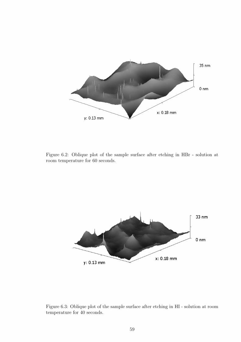
Figure 6.2: Oblique plot of the sample surface after etching in HBr - solution atroom temperature for 60 seconds.
Figure 6.3: Oblique plot of the sample surface after etching in HI - solution at roomtemperature for 40 seconds.
59
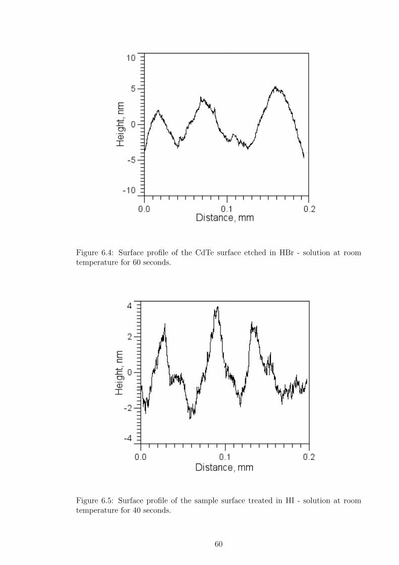
Figure 6.4: Surface profile of the CdTe surface etched in HBr - solution at roomtemperature for 60 seconds.
Figure 6.5: Surface profile of the sample surface treated in HI - solution at roomtemperature for 40 seconds.
60

15
20
25
30
35
Con
duct
ivity
(Ω
-1cm
-1)
0 4 8 12 16 20 24 28Time (hour)
10-2
10-1
2
3
4
5678
2
3
4
Cd
pres
sure
(at
m)
Figure 6.6: Four steps of conductivity relaxation of CdTe:Cl at 700C. Small in-crease of σ after PCd step down at 18.2 hour is due to instability of the furnace atthe fast cooling of Cd source. This drawback does not affect the evaluation of D,which is determined at latter period of σt.
6.2 Chemical diffusion in bulk CdTe:Cl
The conductivity relaxation and chemical diffusion have been measured in relatively
narrow temperature interval 600-700C. The reason is in a large activation energy of
diffusion found in this material. Above 700C the relaxation is too fast to stabilise
PCd satisfactorily before the dominant part of relaxation occurs. Below 600C the
delay to reach the final state has extended up to several days and the sample became
unstable during the long delay, when several relaxation cycles had to be measured.
Typical profile of σt at 700C is plotted in Figure 6.6.
Prior the analysis of D the defect equilibrium has been studied. The theory
outlined in section 1.4 has been used to describe measured conductivity and results
are shown in Figure 6.7. An excellent fit has been obtained taking total Cl density
[Cl]=4 × 1018 cm−3 and A-centre formation energy EA = −0.38 eV , when other
parameters remained unchanged as established in undoped CdTe. The evaluated
[Cl] is close to the intentional doping of the melt, which is probably caused by a fast
solidification and minimised segregation of Cl into melt. Analogous Cl doping of
the melt used in [117] resulted in significantly lower [Cl] found in the solid CdTe:Cl.
61
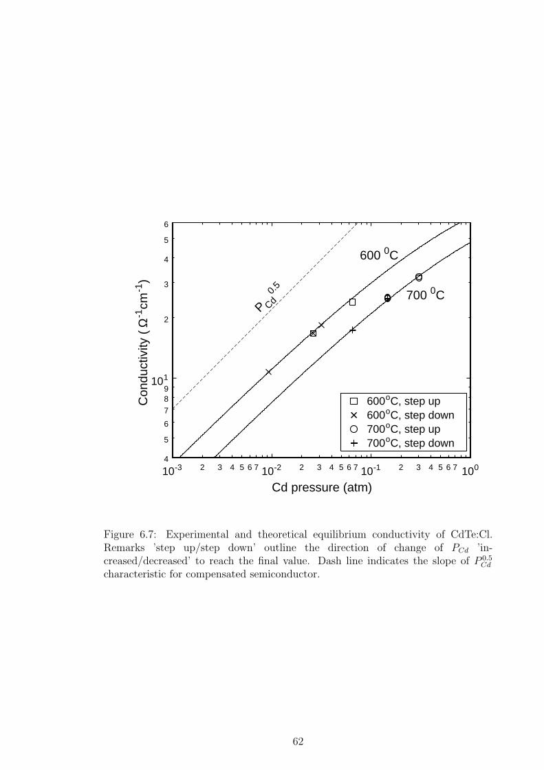
10-3 10-2 10-1 1002 3 4 5 6 7 2 3 4 5 6 7 2 3 4 5 6 7
Cd pressure (atm)
101
4
5
6
7 8 9
2
3
4
5
6
Con
duct
ivity
(Ω
-1cm
-1)
600oC, step up600oC, step down 700oC, step up700oC, step down
600 0C
700 0CP Cd
0.5
Figure 6.7: Experimental and theoretical equilibrium conductivity of CdTe:Cl.Remarks ’step up/step down’ outline the direction of change of PCd ’in-creased/decreased’ to reach the final value. Dash line indicates the slope of P 0.5
Cd
characteristic for compensated semiconductor.
62
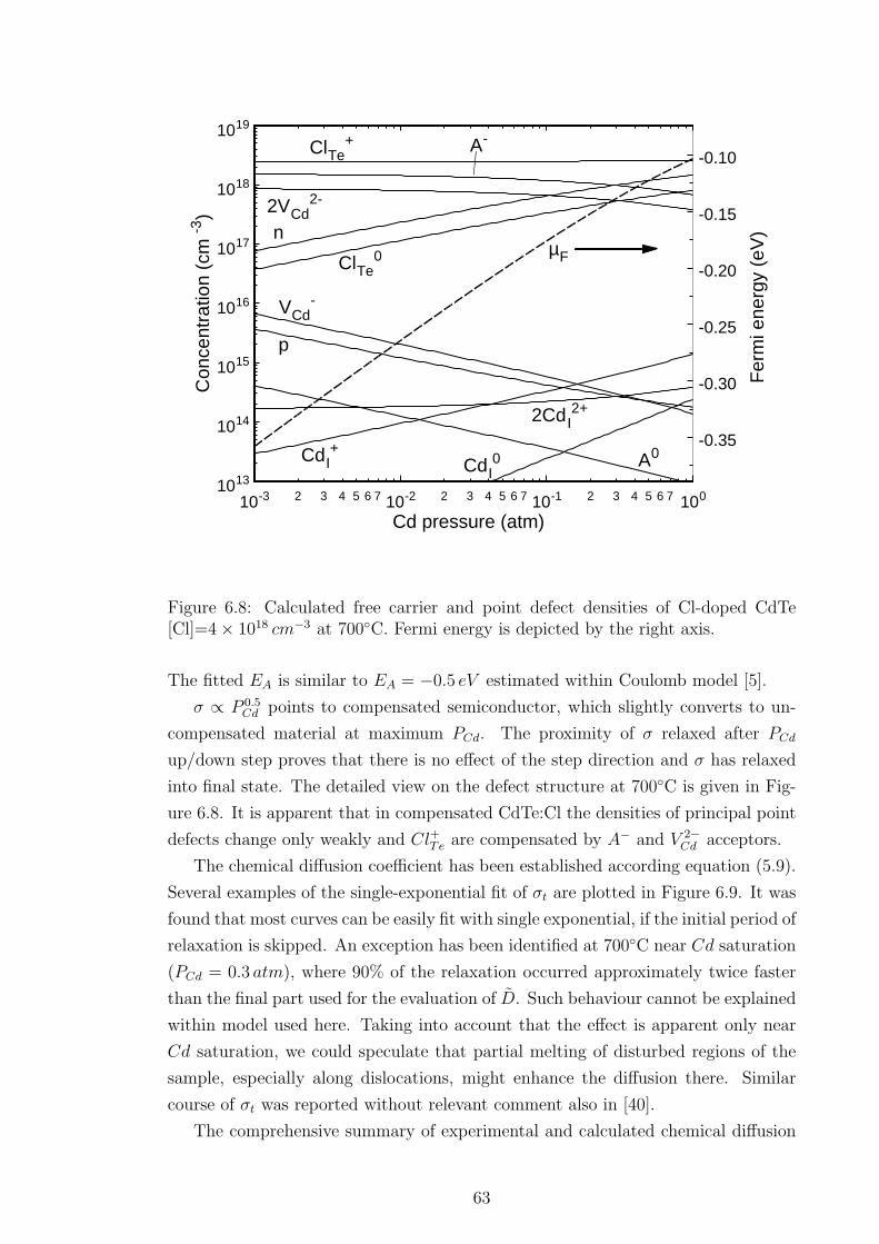
10-3 10-2 10-1 1002 3 4 5 6 7 2 3 4 5 6 7 2 3 4 5 6 7
Cd pressure (atm)
1013
1014
1015
1016
1017
1018
1019
Con
cent
ratio
n (c
m-3
)
CdI0
p
nµF
-0.35
-0.30
-0.25
-0.20
-0.15
-0.10
Fer
mi e
nerg
y (e
V)
CdI+
2CdI2+
VCd-
2VCd2-
A-
A0
ClTe+
ClTe0
Figure 6.8: Calculated free carrier and point defect densities of Cl-doped CdTe[Cl]=4× 1018 cm−3 at 700C. Fermi energy is depicted by the right axis.
The fitted EA is similar to EA = −0.5 eV estimated within Coulomb model [5].
σ ∝ P 0.5Cd points to compensated semiconductor, which slightly converts to un-
compensated material at maximum PCd. The proximity of σ relaxed after PCd
up/down step proves that there is no effect of the step direction and σ has relaxed
into final state. The detailed view on the defect structure at 700C is given in Fig-
ure 6.8. It is apparent that in compensated CdTe:Cl the densities of principal point
defects change only weakly and Cl+Te are compensated by A− and V 2−Cd acceptors.
The chemical diffusion coefficient has been established according equation (5.9).
Several examples of the single-exponential fit of σt are plotted in Figure 6.9. It was
found that most curves can be easily fit with single exponential, if the initial period of
relaxation is skipped. An exception has been identified at 700C near Cd saturation
(PCd = 0.3 atm), where 90% of the relaxation occurred approximately twice faster
than the final part used for the evaluation of D. Such behaviour cannot be explained
within model used here. Taking into account that the effect is apparent only near
Cd saturation, we could speculate that partial melting of disturbed regions of the
sample, especially along dislocations, might enhance the diffusion there. Similar
course of σt was reported without relevant comment also in [40].
The comprehensive summary of experimental and calculated chemical diffusion
63

0 10 20 30 40 50Time (hour)
10-2
10-1
100
(σt−
σ ∞)/(
σ 0−σ
∞)
T=6000C, PCd=0.030 atm, step downT=6000C, PCd=0.026 atm, step upT=7000C, PCd=0.15 atm, step downT=7000C, PCd=0.15 atm, step upT=7000C, PCd=0.3 atm, step up
0 1 2 3 4Time (hour)
Figure 6.9: Single-exponential fit of the conductivity relaxation at conditions givenin the legend. The time of relaxation at 600C/700C is depicted by the bot-tom/upper time axis.
64
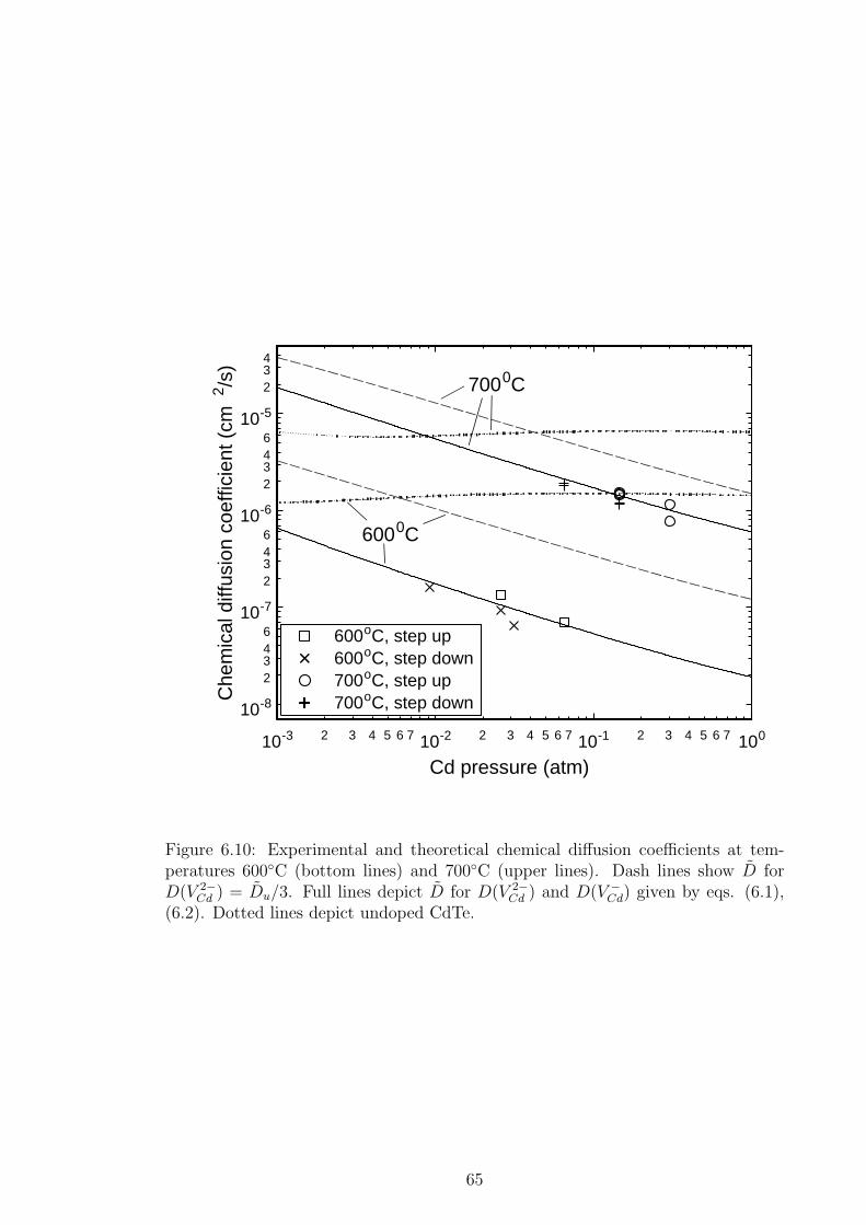
10-3 10-2 10-1 1002 3 4 5 6 7 2 3 4 5 6 7 2 3 4 5 6 7
Cd pressure (atm)
10-8
10-7
10-6
10-5
2 3 4 6
2 3 4 6
2 3 4 6
2 3 4
Che
mic
al d
iffus
ion
coef
ficie
nt (
cm2 /s
)
600oC, step up600oC, step down700oC, step up700oC, step down
7000C
6000C
Figure 6.10: Experimental and theoretical chemical diffusion coefficients at tem-peratures 600C (bottom lines) and 700C (upper lines). Dash lines show D forD(V 2−
Cd ) = Du/3. Full lines depict D for D(V 2−Cd ) and D(V −
Cd) given by eqs. (6.1),(6.2). Dotted lines depict undoped CdTe.
65

coefficients is presented in Figure 6.10. Let us pay the attention to experimental
data at first. Though the interval of PCd is relatively narrow, it is apparent that
D ∝ P−0.5Cd as was predicted in equation (2.22). The relaxation after step up/down
yields distinct D. This ’memory effect’ cannot be explained in standard diffusion
theory. We expect that the effect enhances with poorer quality of the material,
its homogeneity, purity or crystallinity. Comparing with other reports [118] the
relaxation time ratio τ+/τ− ≈ 0.8 observed here is insignificant.
Having defect properties determined by the fit of equilibrium transport data,
the calculation of D according equation (2.21) is limited by unsettled diffusion co-
efficients of involved diffusing point defects. The first trial to express D was done
according [51] taking diffusion coefficients of all diffusing native defects equal to
Du/3. The point of this approach stems from the fact that measured Du in undoped
CdTe is independent of PCd and this choice allows to accomplish satisfactorily such
a result. Respective D are outlined in Figure 6.10 by dash lines. We see that D
exhibits the proper slope D ∝ P−0.5Cd . The magnitude, however, deviates from ex-
perimental points. Due to V 2−Cd is the only principal native defect driving diffusion
in CdTe:Cl, see equation (2.22), the unique parameter to be tuned D(V 2−Cd ) remains.
In parallel, the demand of PCd independent Du can be fulfilled with complementary
optimisation of D(V −Cd). The final fits of D and Du are plotted in Figure 6.10 by
full and dotted lines, respectively, that have been obtained with
D(V2−Cd) = 2.8× 10³ e
− 1.82 eVkBT cm2/s, (6.1)
D(V−Cd) = 4× 10⁻⁴ e− 0.2 eV
kBT cm2/s. (6.2)
Regardless completion of all demands put on the fit and excellent agreement
with experiment, diffusion coefficients (6.1), (6.2) must be analysed with care. Let
us concentrate on D(V 2−Cd ) at first. This parameter expresses a very good agreement
with that evaluated from self-diffusion data in CdTe [36]
D(V2−Cd) =
2.74× 10³
fc
e− 1.85 eV
kBT cm2/s, (6.3)
where the correlation factor fc ≈ 1. Taking into account that equation (6.3) was not
implicitly used at the calculations, its proximity to equation (6.1) strongly supports
defect model used. On the contrary, the fit of D(V −Cd) looks rather artificial. There
is no principal argument for big difference from D(V 2−Cd ) and an alternative approach
should be searched as well. One of the possibilities to make the model more realistic
is the involvement of another native defect abandoned here till now. Fast diffusing
Te interstitial TeI could be a good candidate for that. This native defect was skipped
out in defect models due to its equivalence with VCd in defect chemistry reaction
66

constants, which makes it hardly distinguishable, and larger formation energy [20,
119] making TeI suppressed. Contingent enhanced D(TeI) would, however, bring
TeI to the central attention.
The numerical results based on relatively troublesome calculations are conve-
niently represented by the form
D =1.5× 10⁷√PCd(atm)
e− 2.55 eV
kBT cm2/s, (6.4)
which expresses significantly larger activation energy of diffusion 2.55 eV in CdTe:Cl
relatively to 1.15 eV (equation 2.6) found in undoped CdTe.
6.3 Properties of the contacts
The subjects of this study were electrical contacts on the semi-insulating cadmium
telluride. Dependence of the contact properties on the metal nature, deposition
technique, and anterior surface treatment were studied in details. Samples were
etched using techniques described in section 5.3.1. Deposition of the contacts was
made as described in sections 5.4.2 and 5.4.3. Four types of contacts were prepared:
• deposited from the solution gold - Auch;
• deposited from the solution platinum - Ptch;
• thermally deposited gold - Auth;
• thermally deposited indium - Inth.
Current-voltage characteristics of the contacts were measured at room temperature
in accordance with section 5.5.4. To assure reproducibility of the results, measure-
ment were independently repeated. Each curve represents data obtained out of 8
measurements.
A relative quantity Rsp was introduced for the evaluation of the contacts quality.
It was defined as
Rsp =t+
t−, (6.5)
where t+/− represents the slope of the direct/reverse current-voltage characteristic
near the maximum voltage.
6.3.1 Three-terminal versus two-terminal I-V technique
For this particular measurements samples were etched in standard 3% Br-methanol
solution. Gold contacts were deposited from the aqueous solution. Measurements
were made at room temperature.
67

-4
-3
-2
-1
0
1
2
3
4
-100 -50 0 50 100
Cur
rent
, nA
Voltage, V
3-terminal2-terminal
Figure 6.11: Comparison of the current-voltage characteristics of the gold contact onthe n-type sample treated in the Br-solution obtained using three- and two-terminalmethods.
A comparative two- and three-terminal I-V measurement showed the benefit of
the latter method for the investigation of the properties of the single contact. As
shown in Figure 6.11 in the two-terminal method the curve is roughly symmetric,
but the three-terminal method proves that the contacts are non-ohmic. This is
because of the circuit arrangement. All contacts are metal-semiconductor junctions.
In case of two-terminal measurements the properties of two junctions connected in
the opposite direction are measured jointly leading to the lost of information about
each of the terminals. Three-terminal measurement solves this problem by utilizing
third independent electrode for the measurement of potential. As a result, it gives
precise information on each contact separately.
6.3.2 Comparison of various metals as contact materials
Detailed investigation of the properties of metal contacts deposited on CdTe was
done. Both n- and p-type semi-insulating cadmium telluride samples were used.
Four various types of contacts were fabricated. Gold, platinum and indium were
employed as contact materials. In case of Au two deposition techniques were used,
namely thermal evaporation and deposition from aqueous solution. Surfaces of all
samples were prepared by the same technique, including chemical-mechanical pol-
ishing and treatment in etching solution.
68

-30
-20
-10
0
10
20
30
-100 -50 0 50 100
Cur
rent
, nA
Voltage, V
Au (thermal)In (thermal)
Au (chemical)Pt (chemical)
Figure 6.12: Comparison of the current-voltage characteristics of the metal-semiconductor junctions prepared on n-CdTe. Sample surface was treated in stan-dard bromine-methanol solution. Contacts were prepared using various metals andtechniques: - thermally evaporated Au; - thermally evaporated In; ♦ - Audeposited from the aqueous solution; - Pt deposited from the aqueous solution.
A comparison of the properties of the contacts made out of various metals on the
n-type cadmium telluride etched in 3% Br-methanol solution is shown on Figure 6.12.
Current-voltage characteristic of the indium contact is close to linear. Characteristic
curves representing Auth, Auch, and Ptch contacts are different. In the negative bias
all the three behave according to Ohm’s law. Linear dependencies of the current on
applied voltage have only different slopes. This points on different contact resistance.
For the positive bias stronger increase of current is observed.
Concave shaped I-V curves under forward bias are observed on most Au and
Pt contacts fabricated on n-CdTe. For such anomalous behaviour we propose two
possible explanations described in Section 6.3.4. In case of surface treated in HBr-
solution characteristics obtained for platinum and gold contacts are linear in reverse
bias and concave under forward bias (Figure 6.13). Indium contact characteristic is
slightly S-shaped and has the resistance one order of magnitude lower than other
contacts. For better visibility it is depicted separately by the right axis. Despite
not been ideally ohmic Inth contact has the best comparative quality.
On surfaces etched in HI-based etching solution again anomalous current-voltage
characteristics with concave shapes are obtained under forward bias (Figure 6.14).
Only Inth contacts behave according to Ohm’s law. Resistance of the indium contact
69
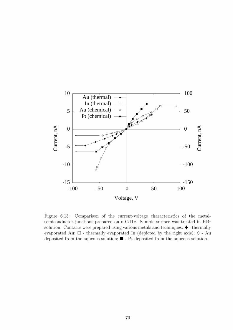
-15
-10
-5
0
5
10
-100 -50 0 50 100-150
-100
-50
0
50
100
Cur
rent
, nA
Cur
rent
, nA
Voltage, V
Au (thermal)In (thermal)
Au (chemical)Pt (chemical)
Figure 6.13: Comparison of the current-voltage characteristics of the metal-semiconductor junctions prepared on n-CdTe. Sample surface was treated in HBrsolution. Contacts were prepared using various metals and techniques: - thermallyevaporated Au; - thermally evaporated In (depicted by the right axis); ♦ - Audeposited from the aqueous solution; - Pt deposited from the aqueous solution.
70

-4
-3
-2
-1
0
1
2
3
4
-100 -50 0 50 100-20
-15
-10
-5
0
5
10
15
20
Cur
rent
, nA
Cur
rent
, nA
Voltage, V
Au (thermal)In (thermal)
Au (chemical)Pt (chemical)
Figure 6.14: Comparison of the current-voltage characteristics of the metal-semiconductor junctions prepared on n-CdTe. Sample surface was treated in HIsolution. Contacts were prepared using various metals and techniques: - ther-mally evaporated Au; - thermally evaporated In (depicted by the right axis); ♦ -Au deposited from the aqueous solution; - Pt deposited from the aqueous solution.
is 5 times lower from the resistances of contacts made out of the other metals.
It is clear that on SI CdTe with n-type conductivity thermally deposited indium
forms contacts with the smallest resistivity. Among the compared materials they
are the only contacts to have I-V characteristics close to linear.
Contacts prepared on CdTe with p-type conductivity behave totally different.
In most cases ohmic contacts are obtained. This is expressed in linear character
of the I-V curves. The difference between this contacts is mainly in the resistance.
Thus, this parameter is chosen to be the determinative in the comparison of various
contact preparation techniques on p-type cadmium telluride.
Lets take a look at cases with different surface treatments. Contacts, prepared on
p-CdTe etched in standard bromine-methanol solution, are ohmic (Figure 6.15) with
exception of contacts prepared by thermal evaporation of indium. Current-voltage
characteristic of this particular contact is not linear, but has an S-shape profile.
For other contacts (Auth, Auch, and Ptch) linear dependencies of current on applied
voltage are obtained. In case of thermally evaporated gold and deposited from the
aqueous solution platinum obtained I-V curves are identical with small deviations
from each other. The best properties among contacts with ohmic behaviour has the
gold contact deposited from solution. It has the higher slope value of the current-
71

-100-80-60-40-20
0 20 40 60 80
100
-100 -50 0 50 100
Cur
rent
, nA
Voltage, V
Au (thermal)In (thermal)
Au (chemical)Pt (chemical)
Figure 6.15: Comparison of the current-voltage characteristics of the metal-semiconductor junctions prepared on p-CdTe. Sample surface was treated in stan-dard bromine-methanol solution. Contacts were prepared using various metals andtechniques: - thermally evaporated Au; - thermally evaporated In; ♦ - Audeposited from the aqueous solution; - Pt deposited from the aqueous solution.
voltage dependence indicating the smaller contact resistance.
Slightly different results are obtained in case of contacting surfaces treated in HBr
- solution (Figure 6.16). Three types of contacts have similar properties. Namely
Ptch, Auth, and Inth. All of them show behaviour close to ohmic. Current-voltage
characteristics for the first two (Ptch and Auth) have small deviation from linear.
I-V curve of the indium contact has slight S-shape profile. Gold contact deposited
from solution proves to be the best on this particular surface. It is perfectly ohmic
with the lowest resistivity among compared materials.
The worst result is obtained for the Inth contact prepared on p-type CdTe sur-
face treated in HI - solution (Figure 6.17). Its resistance is found to be one order
of magnitude higher than resistance of other contacts studied in our experiment.
Current-voltage characteristics of Auth, Auch, and Ptch contacts are close to linear
and had similar slope values.
As we can see in case of p-type cadmium telluride thermally evaporated indium
contacts exhibit poor behaviour, the worst among contacts compared in our inves-
tigation.
72
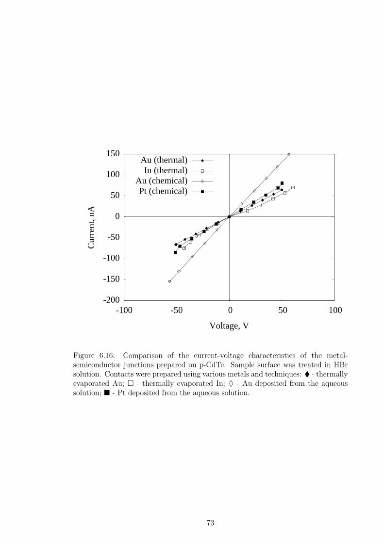
-200
-150
-100
-50
0
50
100
150
-100 -50 0 50 100
Cur
rent
, nA
Voltage, V
Au (thermal)In (thermal)
Au (chemical)Pt (chemical)
Figure 6.16: Comparison of the current-voltage characteristics of the metal-semiconductor junctions prepared on p-CdTe. Sample surface was treated in HBrsolution. Contacts were prepared using various metals and techniques: - thermallyevaporated Au; - thermally evaporated In; ♦ - Au deposited from the aqueoussolution; - Pt deposited from the aqueous solution.
73
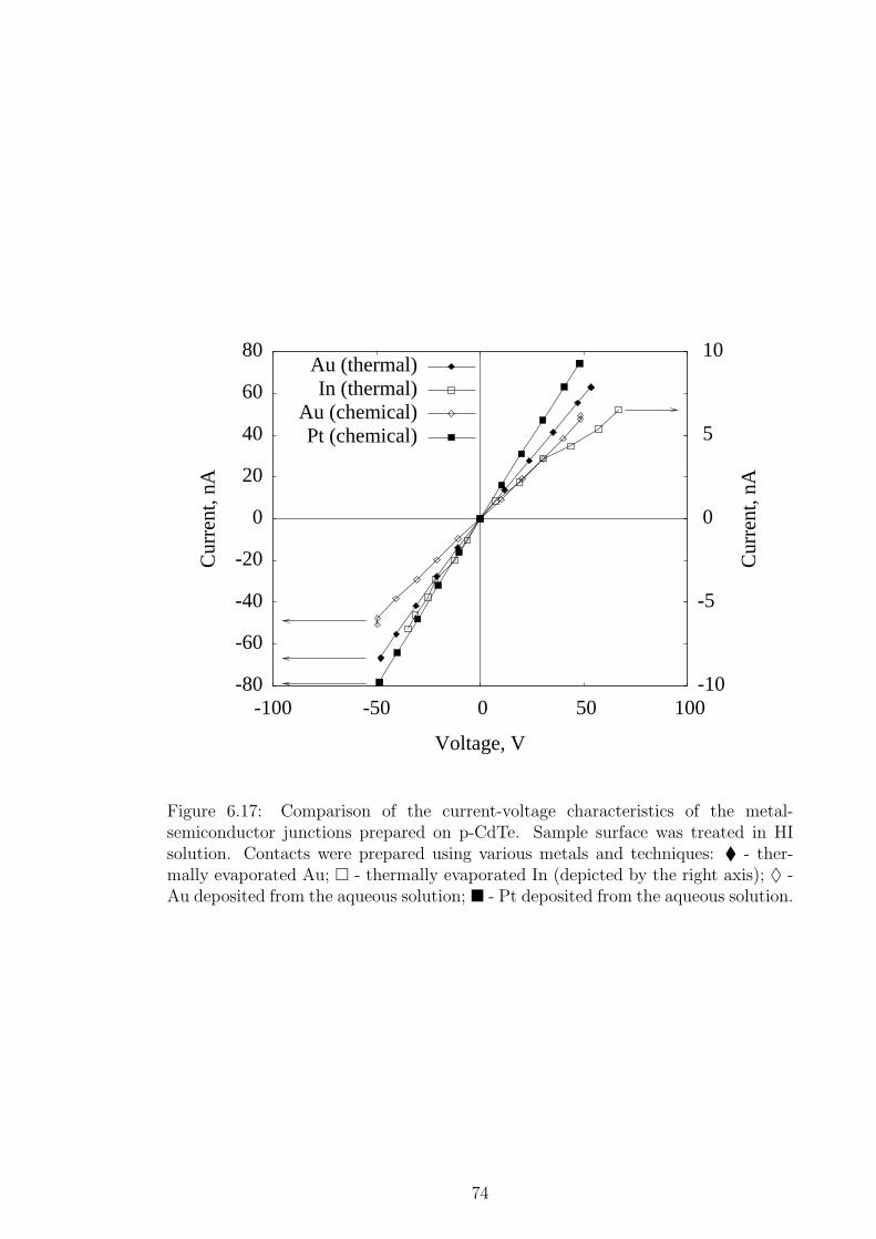
-80
-60
-40
-20
0
20
40
60
80
-100 -50 0 50 100-10
-5
0
5
10
Cur
rent
, nA
Cur
rent
, nA
Voltage, V
Au (thermal)In (thermal)
Au (chemical)Pt (chemical)
Figure 6.17: Comparison of the current-voltage characteristics of the metal-semiconductor junctions prepared on p-CdTe. Sample surface was treated in HIsolution. Contacts were prepared using various metals and techniques: - ther-mally evaporated Au; - thermally evaporated In (depicted by the right axis); ♦ -Au deposited from the aqueous solution; - Pt deposited from the aqueous solution.
74

-150
-100
-50
0
50
100
150
-100 -50 0 50 100-15
-10
-5
0
5
10
15
Cur
rent
, nA
Cur
rent
, nA
Voltage, V
Br-sol.HBr-sol.
HI-sol.
Figure 6.18: Comparison of the current-voltage characteristics of the metal-semiconductor junctions prepared on n-CdTe. Contacts were prepared by the ther-mal evaporation of In. Sample surface was treated in various solutions: - standardbromine-methanol solution (depicted by the right axis); ♦ - HBr solution (depictedby the right axis); - HI solution.
6.3.3 Contact quality depending on the etching solution used
for surface treatment
Contact quality is greatly influenced by the properties of the surface on which metal
is deposited. Chemical polishing and etching change not only the roughness but
also the composition of the surface layer. The purpose of surface treatment is to
remove all inhomogeneities and oxide layer which may form barrier between the
metal and bulk material. It is also important to achieve stoichiometric composition
of the surface to exclude possibility of getting leakage current.
Comparison of the current-voltage characteristics of In contacts thermally de-
posited on the n-type CdTe samples treated in various solutions is shown in Figure
6.18. Despite of deviating from ohmic behaviour, the resistivity of the contact pre-
pared on the sample surface etched in the HI-solution is significantly lower than in
case of the use of other solutions.
Figures 6.19, 6.20, and 6.21 show current-voltage dependencies for the Auth,
Auch, and Ptch contacts respectively. All of them were prepared on n-type CdTe.
Characteristics are similar and in all cases anomalous concave shape in positive bias
region is observed. A discussion of this effect is given in Section 6.3.4.
75

-10
-5
0
5
10
-100 -50 0 50 100
Cur
rent
, nA
Voltage, V
Br-sol.HBr-sol.
HI-sol.
Figure 6.19: Comparison of the current-voltage characteristics of the metal-semiconductor junctions prepared on n-CdTe. Contacts were prepared by the ther-mal evaporation of Au. Sample surface was treated in various solutions: - standardbromine-methanol solution; ♦ - HBr solution; - HI solution.
76
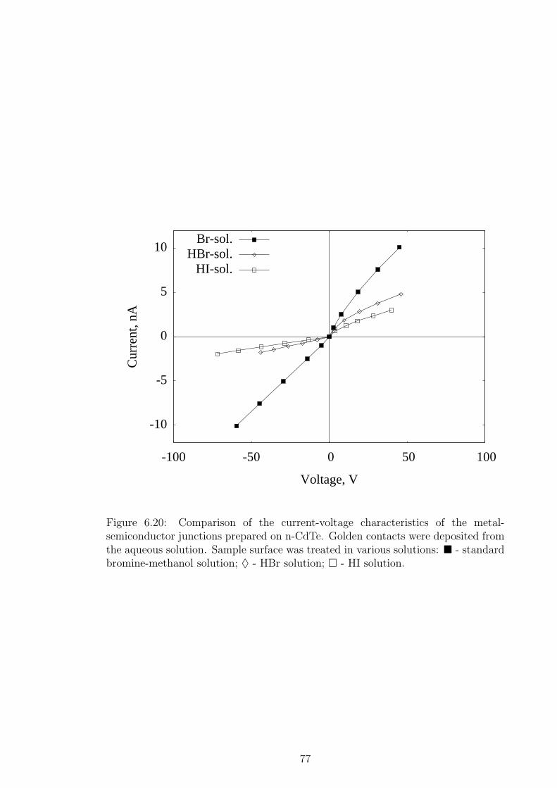
-10
-5
0
5
10
-100 -50 0 50 100
Cur
rent
, nA
Voltage, V
Br-sol.HBr-sol.
HI-sol.
Figure 6.20: Comparison of the current-voltage characteristics of the metal-semiconductor junctions prepared on n-CdTe. Golden contacts were deposited fromthe aqueous solution. Sample surface was treated in various solutions: - standardbromine-methanol solution; ♦ - HBr solution; - HI solution.
77

-10
-5
0
5
10
-100 -50 0 50 100
Cur
rent
, nA
Voltage, V
Br-sol.HBr-sol.
HI-sol.
Figure 6.21: Comparison of the current-voltage characteristics of the metal-semiconductor junctions prepared on n-CdTe. Platinum contacts were depositedfrom the aqueous solution. Sample surface was treated in various solutions: -standard bromine-methanol solution; ♦ - HBr solution; - HI solution.
78
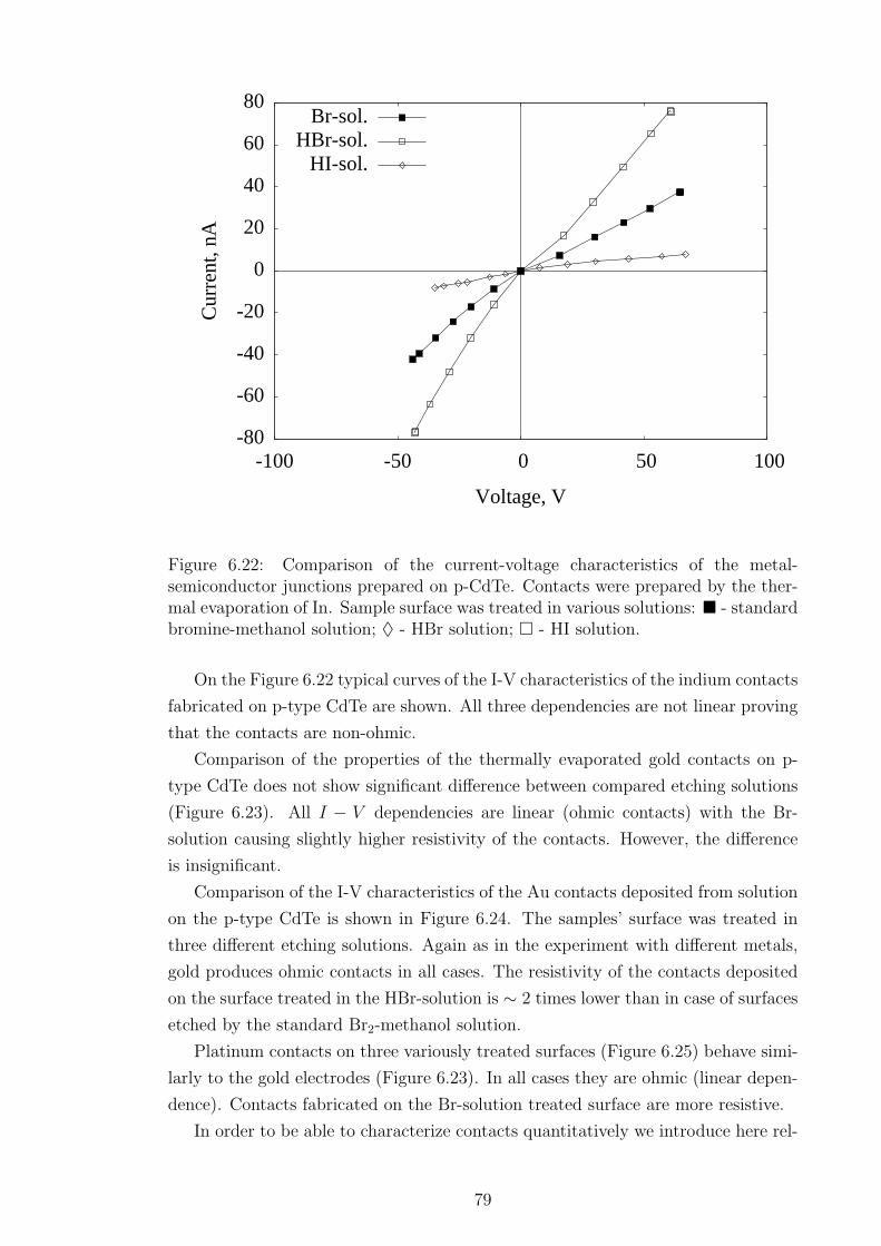
-80
-60
-40
-20
0
20
40
60
80
-100 -50 0 50 100
Cur
rent
, nA
Voltage, V
Br-sol.HBr-sol.
HI-sol.
Figure 6.22: Comparison of the current-voltage characteristics of the metal-semiconductor junctions prepared on p-CdTe. Contacts were prepared by the ther-mal evaporation of In. Sample surface was treated in various solutions: - standardbromine-methanol solution; ♦ - HBr solution; - HI solution.
On the Figure 6.22 typical curves of the I-V characteristics of the indium contacts
fabricated on p-type CdTe are shown. All three dependencies are not linear proving
that the contacts are non-ohmic.
Comparison of the properties of the thermally evaporated gold contacts on p-
type CdTe does not show significant difference between compared etching solutions
(Figure 6.23). All I − V dependencies are linear (ohmic contacts) with the Br-
solution causing slightly higher resistivity of the contacts. However, the difference
is insignificant.
Comparison of the I-V characteristics of the Au contacts deposited from solution
on the p-type CdTe is shown in Figure 6.24. The samples’ surface was treated in
three different etching solutions. Again as in the experiment with different metals,
gold produces ohmic contacts in all cases. The resistivity of the contacts deposited
on the surface treated in the HBr-solution is ∼ 2 times lower than in case of surfaces
etched by the standard Br2-methanol solution.
Platinum contacts on three variously treated surfaces (Figure 6.25) behave simi-
larly to the gold electrodes (Figure 6.23). In all cases they are ohmic (linear depen-
dence). Contacts fabricated on the Br-solution treated surface are more resistive.
In order to be able to characterize contacts quantitatively we introduce here rel-
79
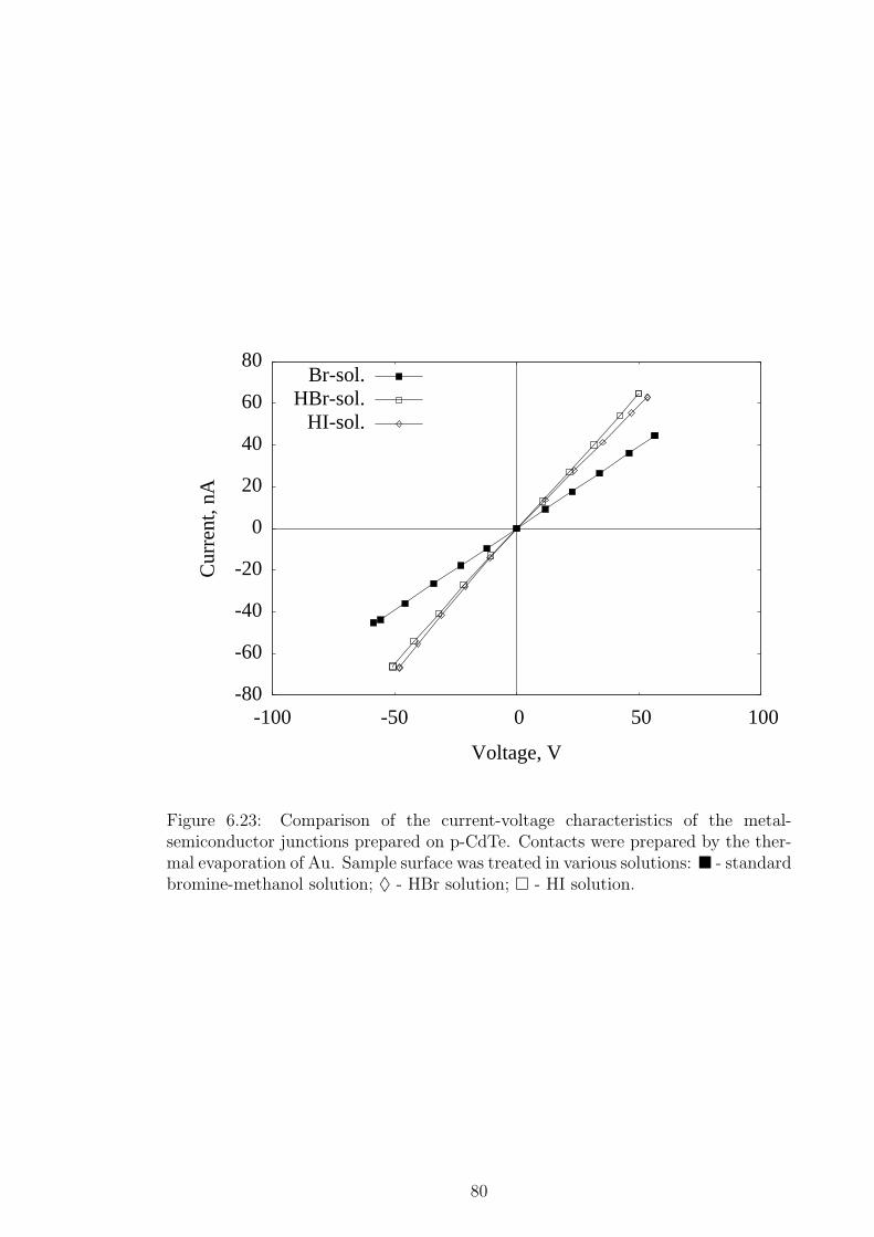
-80
-60
-40
-20
0
20
40
60
80
-100 -50 0 50 100
Cur
rent
, nA
Voltage, V
Br-sol.HBr-sol.
HI-sol.
Figure 6.23: Comparison of the current-voltage characteristics of the metal-semiconductor junctions prepared on p-CdTe. Contacts were prepared by the ther-mal evaporation of Au. Sample surface was treated in various solutions: - standardbromine-methanol solution; ♦ - HBr solution; - HI solution.
80

-200
-150
-100
-50
0
50
100
150
-100 -50 0 50 100
Cur
rent
, nA
Voltage, V
Br-sol.HBr-sol.
HI-sol.
Figure 6.24: Comparison of the current-voltage characteristics of the metal-semiconductor junctions prepared on p-CdTe. Golden contacts were deposited fromthe aqueous solution. Sample surface was treated in various solutions: - standardbromine-methanol solution; ♦ - HBr solution; - HI solution.
81

-120-100-80-60-40-20
0 20 40 60 80
100
-100 -50 0 50 100
Cur
rent
, nA
Voltage, V
Br-sol.HBr-sol.
HI-sol.
Figure 6.25: Comparison of the current-voltage characteristics of the metal-semiconductor junctions prepared on p-CdTe. Platinum contacts were depositedfrom the aqueous solution. Sample surface was treated in various solutions: -standard bromine-methanol solution; ♦ - HBr solution; - HI solution.
82

Table 6.2: Slopes ratios in the region of positive and negative bias.
contact metaldep.tech. Auch Ptch Auth Inth
conductivity type n p n p n p n pBr - solution 0.93 1.03 0.63 0.92 1.08 0.96 1.21 1.74
HBr - solution 0.54 1.04 0.69 1.40 0.53 1.01 3.53 1.60HI - solution 0.58 1.01 0.26 1.06 0.59 1.28 1.30 2.44
ative parameter Rsp. It represents contact rectification property. The value of the
coefficient is a relation between the slope of I-V curve in the forward and reverse
bias. Since current-voltage characteristics are not always linear the slope is calcu-
lated for the maximum voltage area. Other important parameter of the contact is
its resistivity. It is not included into Rsp. Hence, the coefficient cannot be used
for the comparison purpose. It is strictly limited for the characterization of each
single contact. Slope ratios Rsp estimated for all current-voltage measurements are
summarized in Table 6.2. Values close to 1 correspond to ohmic contacts.
The overall inspection of results allows us to conclude that the best contacts on
n-type SI CdTe are prepared with In deposited thermally on the surface treated in
HI-solution. On p-type SI CdTe the best option results in Au deposited chemically
on the surface treated in HBr-solution. The comparison of the contact quality
relevant to n-type/p-type SI CdTe proves the importance of well-known type of the
conductivity to the choice of proper contact preparation treatment. In view of the
fact that the treatment in HI-solution with In contact deposition improves/corrupts
the quality of the contact on n-type/p-type, we can conclude that the treatment
in HI-solution produces a donor-like (electron-rich) interface layer, which properly
links the n-type with In having low work function. On the p-type, oppositely, the
potential barrier is enhanced and the contact quality is worse. Analogous finding can
be deduced for the treatment in HBr-solution where the formation of an acceptor-like
(electron-pure) interface is expected.
6.3.4 Models of the anomalous concave shape of current-
voltage characteristic under forward bias
The measurement of current-voltage characteristics on n-type SI CdTe under forward
bias displays in most cases an anomalous concave form, which is not predicted by
standard theories reviewed in textbooks. For the explanation of that effect we
suggest two models outlined here.
83
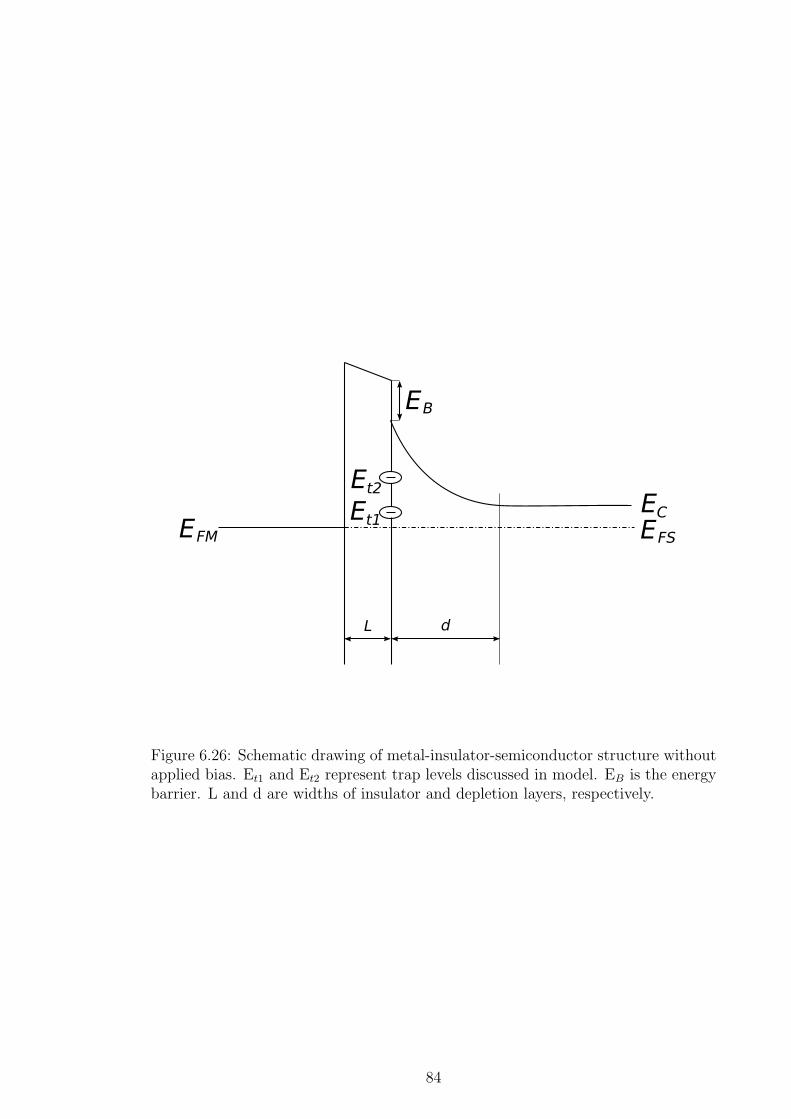
EEFS
CEFM
EB
dL
Et2
Et1
Figure 6.26: Schematic drawing of metal-insulator-semiconductor structure withoutapplied bias. Et1 and Et2 represent trap levels discussed in model. EB is the energybarrier. L and d are widths of insulator and depletion layers, respectively.
84
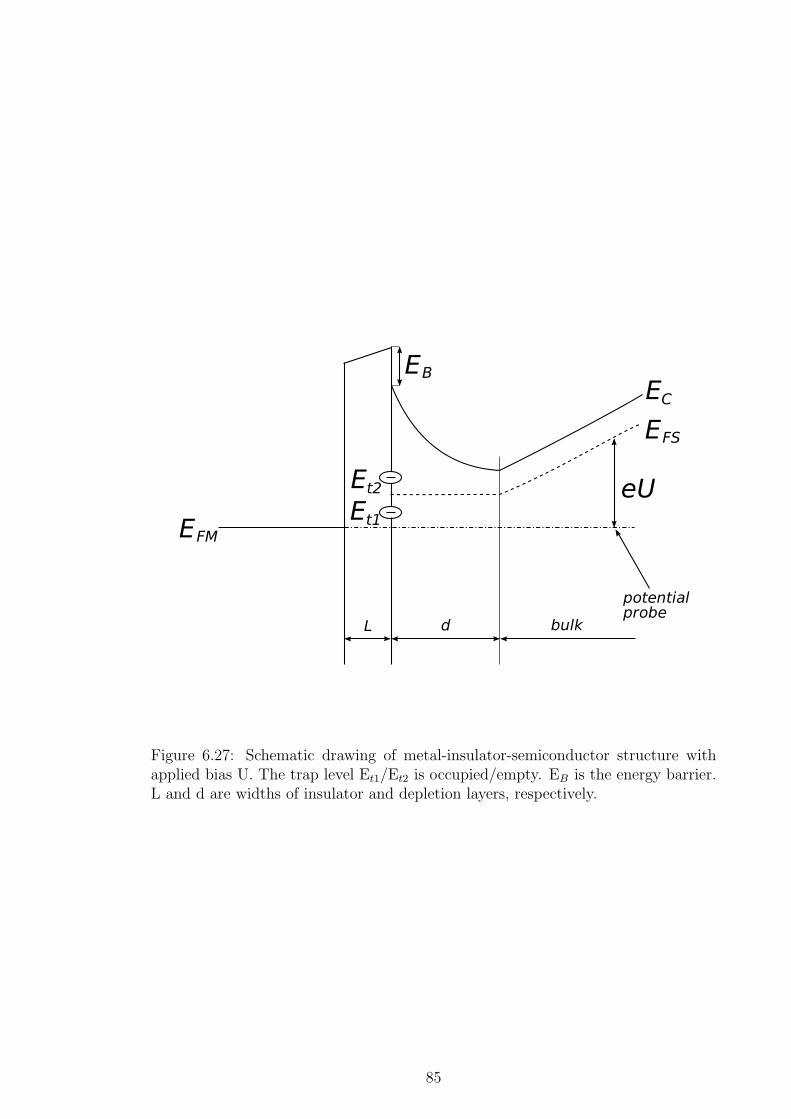
E
EFS
C
EFM
EB
dL
Et2
Et1
eU
potentialprobe
bulk
Figure 6.27: Schematic drawing of metal-insulator-semiconductor structure withapplied bias U. The trap level Et1/Et2 is occupied/empty. EB is the energy barrier.L and d are widths of insulator and depletion layers, respectively.
85
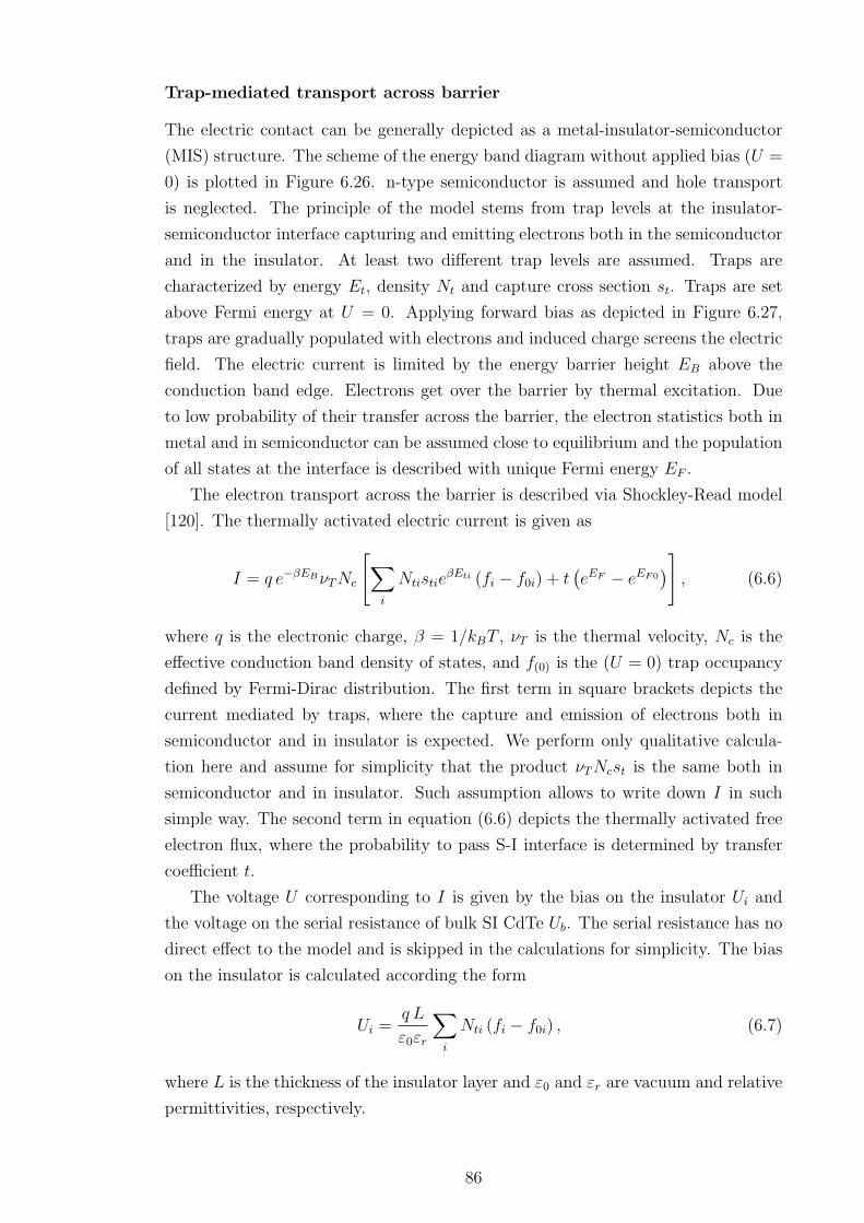
Trap-mediated transport across barrier
The electric contact can be generally depicted as a metal-insulator-semiconductor
(MIS) structure. The scheme of the energy band diagram without applied bias (U =
0) is plotted in Figure 6.26. n-type semiconductor is assumed and hole transport
is neglected. The principle of the model stems from trap levels at the insulator-
semiconductor interface capturing and emitting electrons both in the semiconductor
and in the insulator. At least two different trap levels are assumed. Traps are
characterized by energy Et, density Nt and capture cross section st. Traps are set
above Fermi energy at U = 0. Applying forward bias as depicted in Figure 6.27,
traps are gradually populated with electrons and induced charge screens the electric
field. The electric current is limited by the energy barrier height EB above the
conduction band edge. Electrons get over the barrier by thermal excitation. Due
to low probability of their transfer across the barrier, the electron statistics both in
metal and in semiconductor can be assumed close to equilibrium and the population
of all states at the interface is described with unique Fermi energy EF .
The electron transport across the barrier is described via Shockley-Read model
[120]. The thermally activated electric current is given as
I = q e−βEBνT Nc
[∑i
NtistieβEti (fi − f0i) + t
(eEF − eEF0
)], (6.6)
where q is the electronic charge, β = 1/kBT , νT is the thermal velocity, Nc is the
effective conduction band density of states, and f(0) is the (U = 0) trap occupancy
defined by Fermi-Dirac distribution. The first term in square brackets depicts the
current mediated by traps, where the capture and emission of electrons both in
semiconductor and in insulator is expected. We perform only qualitative calcula-
tion here and assume for simplicity that the product νT Ncst is the same both in
semiconductor and in insulator. Such assumption allows to write down I in such
simple way. The second term in equation (6.6) depicts the thermally activated free
electron flux, where the probability to pass S-I interface is determined by transfer
coefficient t.
The voltage U corresponding to I is given by the bias on the insulator Ui and
the voltage on the serial resistance of bulk SI CdTe Ub. The serial resistance has no
direct effect to the model and is skipped in the calculations for simplicity. The bias
on the insulator is calculated according the form
Ui =q L
ε0εr
∑i
Nti (fi − f0i) , (6.7)
where L is the thickness of the insulator layer and ε0 and εr are vacuum and relative
permittivities, respectively.
86
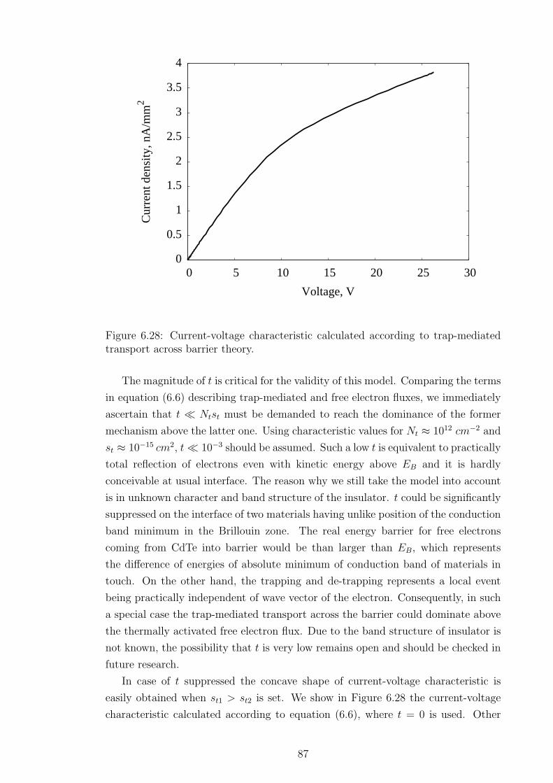
0
0.5
1
1.5
2
2.5
3
3.5
4
0 5 10 15 20 25 30
Cur
rent
den
sity
, nA
/mm
2
Voltage, V
Figure 6.28: Current-voltage characteristic calculated according to trap-mediatedtransport across barrier theory.
The magnitude of t is critical for the validity of this model. Comparing the terms
in equation (6.6) describing trap-mediated and free electron fluxes, we immediately
ascertain that t Ntst must be demanded to reach the dominance of the former
mechanism above the latter one. Using characteristic values for Nt ≈ 1012 cm−2 and
st ≈ 10−15 cm2, t 10−3 should be assumed. Such a low t is equivalent to practically
total reflection of electrons even with kinetic energy above EB and it is hardly
conceivable at usual interface. The reason why we still take the model into account
is in unknown character and band structure of the insulator. t could be significantly
suppressed on the interface of two materials having unlike position of the conduction
band minimum in the Brillouin zone. The real energy barrier for free electrons
coming from CdTe into barrier would be than larger than EB, which represents
the difference of energies of absolute minimum of conduction band of materials in
touch. On the other hand, the trapping and de-trapping represents a local event
being practically independent of wave vector of the electron. Consequently, in such
a special case the trap-mediated transport across the barrier could dominate above
the thermally activated free electron flux. Due to the band structure of insulator is
not known, the possibility that t is very low remains open and should be checked in
future research.
In case of t suppressed the concave shape of current-voltage characteristic is
easily obtained when st1 > st2 is set. We show in Figure 6.28 the current-voltage
characteristic calculated according to equation (6.6), where t = 0 is used. Other
87

Table 6.3: Basic parameters used at the calculations according to trap-mediatedtransport across barrier model
parameter valueNt1 5× 1011 cm−2
Et1 −0.46 eVst1 10−13 cm2
Nt2 1012 cm−2
Et2 −0.38 eVst2 10−15 cm2
EB 0.25 eVEF0 −0.6 eVT 295 KνT 3.8× 107 cm/sεr 10.3L 1 µm
parameters are given in Table 6.3.
Extended depletion of CdTe bulk
The dominant problem in the preparation of room temperature (RT) gamma and
x-ray detectors on CdTe is comprised in apparently contradictory demands of a low
free carrier density, which has to be close to intrinsic carrier density ni ≈ 106 cm−3
in CdTe at RT, and the high carrier mobility-lifetime product (µτ), which cannot be
reached without significant reduction of trapping centres in the crystal. Even in the
best quality materials the controlled density of shallow defects does not decrease
below 1015 cm−3. To avoid considerable loss of photo-generated carriers and the
depreciation of the detector, the deep trap density Nt < 1013 cm−3 with trapping
cross section s = 10−15 cm2 is necessary [121].
Straightforward procedure to figure out this problem is based on the search of
a deep defect with the ionization level near the middle of the band gap (mid-gap)
and with s < 10−17 cm2. Such defect introduced into the material at the density
Ndeep ∼ 1015 cm−3 would compensate the shallow defects and pin the Fermi energy
near the mid-gap without strong trapping and degradation of µτ [122]. Recent
experimental findings, however, do not support such a scheme and show s of mid-
gap levels in the range of 10−14 − 10−13 cm2 or even up to 10−11 cm2 [123, 124].
The fact that high quality detectors on CdTe exist points to some underestimated
processes at the detector fabrication, which result in significant shallow level self-
compensation and a formation of SI CdTe even if Nt < 1012 cm−3. The assumption
of a very low Nt in the SI CdTe bulk forms the basis of this model.
The measurement of the contact under forward bias entails the reverse bias
applied to the counterpart. Due to the depletion layer spreads from that reverse
88

-2
-1.5
-1
-0.5
0
0.5
1
1.5
2
-100 -80 -60 -40 -20 0 20 40
Cur
rent
den
sity
, nA
/mm
2
Voltage, V
0.08 Eg0.04 Eg
Figure 6.29: Current-voltage characteristics calculated according to extended de-pletion model. The labels show the band banding at the surface forming depletionlayer.
contact into the bulk, it can reach at large enough voltage the area of the potential
contact and affect the resistivity adjudged to the contact under forward bias.
For the analysis of the effects outlined above we have utilized the experience
gained by our group at the research of SI CdTe in the past 15 years and an extensive
library of computer programs for simulation of transport processes in SI CdTe. The
electron transport in the structure with extended depletion region was simulated
with the code solving self-consistently one-dimensional coupled drift-diffusion and
Poisson’s equations including generation-recombination processes on impurity levels
described within Hall-Shockley-Read model. Details of the approach are presented
in [125]. Band-bending below contacts is set by Fermi energy at the surface. Two
examples of the calculated current-voltage characteristics are plotted in Figure 6.29.
Parameters used at the calculations are given in Table 6.4. The second deep level put
significantly below Fermi energy was used to increase the electric current without
enormous charging of the level. It is apparent, that the calculated curves depict well
the measured data and the model can be used as good basis for the explanation of
the observed effect.
Summarizing positives and negatives of suggested models, both models explain
the concave shape in current-voltage characteristics under forward bias. The former
model suffers from necessary suppression of free-electron transport through the in-
sulating barrier, the latter model requests very low density of deep levels to allows
89

Table 6.4: Basic parameters used at the calculations according to extended depletiontheory. Items (a), (b) correspond to thin and thick lines in Figure 6.29, respectively.
parameter valuesample thickness 2 mm1st deep level energy Ec − 0.46 Eg
1st deep level density 1011 cm−3
1st deep level electron capture cross section 10−12 cm2
1st deep level hole capture cross section 10−12 cm2
2nd deep level energy Ec − 0.6 Eg
2nd deep level density 1014 cm−3
2nd deep level electron capture cross section 10−11 cm2
2nd deep level hole capture cross section 10−13 cm2
equilibrium Fermi energy EF0 Ec − 0.42 Eg
Fermi energy at the surface Ec − 0.5 Eg (a)Ec − 0.46 Eg (b)
the formation of extensive depletion layer at the reversed contact.
6.3.5 Capacitance-voltage measurements
All treatments of the CdTe samples were performed in the air atmosphere. Under
such conditions surface is covered with thin oxide layer. By fabricating metal con-
tacts on such surface metal-oxide-semiconductor (MOS) structure is formed. The
exact thickness of the oxide layer is not known. Moreover, the exact structure of
the semiconductor surface is unknown.
Properties of interface traps distributed in the semiconductor band-gap are con-
veniently studied with admittance measurements [126]. Capacitance-voltage mea-
surements were performed as described in Section 5.5.5. For the admittance mea-
surement we have prepared samples with design outlined in Figure 6.30, which is
conventionally used in this case. Samples dimensions were 5× 5× 2 mm. Contacts
1 and 2 were 4 × 4 mm. N-type SI CdTe sample contacted with gold to build de-
pletion layer at the interface have been chosen. Due to the apparatus allowed to
apply maximum 10 volts to the circuit, the bias did not manipulate interface charge
markedly and no voltage dependence has been observed. Thus, we analyse only
frequency dependence in this chapter.
Collected data are analysed according equivalent circuit plotted in Figure 6.31
characterized by the admittance
Y0 = G + 2πjfC. (6.8)
The course of the capacity and resistivity evaluated according the equivalent circuit
is shown in Figures 6.32 and 6.33. The capacitance C has been excellently fit with
90

1
3
2
Figure 6.30: Sample design with three gold contacts for C − V measurements.Alternating current is applied on contacts 1 − 2. Voltage is measured on 1 − 3contacts.
C
G
Figure 6.31: Equivalent circuit used by the Agilent E4980A Precision LCR Meterfor the data analysis.
91

10-12
10-11
10-10
10-9
10-8
102 103 104 105 106
Cap
acita
nce,
F
Frequence, Hz
3
2
1
Figure 6.32: Dependence of contact capacitance on frequency. Experimental dataare depicted with open squares. Thick line represents theoretical fit. 1, 2, 3 corre-spond to the first, second and third trap levels, respectively.
trial function
Ct = 6.1× 10⁻⁶f−1.6 + 3.1× 10⁻¹¹. (6.9)
Two samples have been measured and similar characteristics were obtained.
For the interpretation of measured data we follow [126] and describe the struc-
ture according MOS (Metal-Oxide-Semiconductor) equivalent circuit as shown in
Figure 6.34, where parallel combination of Gi, Ci branches represent ith trap level
localized near interface. Ci is the capacitance of the ith interface level, and Gi is
the corresponding electron capture conductance. The admittance of the circuit is
calculated according the form
Y =∑
i
(2πfCi)2/Gi
1 + (2πfCi/Gi)2+ 2πjf
(C0 +
∑i
Ci
1 + (2πfCi/Gi)2
), (6.10)
where the sum counts respective branches of the circuit representing distinct trap
levels. Comparing real and imaginary parts of equations (6.8) and (6.10), we imme-
diately obtain G and C corresponding to the equivalent circuit.
Very good fit of both C and G presented in Figures 6.32 and 6.33 has been
obtained taking three trap levels with parameters shown in Table 6.5. The parallel
92

0
1
2
3
4
5
6
7
8
9
102 103 104 105 106
Con
duct
ance
, MΩ
-1
Frequence, Hz
3
2
1
Figure 6.33: Dependence of contact resistance on frequency. Experimental data areplotted with open squares. Thick line shows theoretical fit. 1, 2, 3 correspond tothe first, second and third trap levels, respectively.
C G1 1
C G2 2
C G3 3
C Gi i
C0
Figure 6.34: Alternative equivalent circuit used for the admittance analysis.
93

Table 6.5: Fitting parameters for the capacitance and admittance of the gold con-tacts on SI CdTe.
parameter valueC1 28 nFG1 6.5× 10⁻⁶ Ω−1
C2 0.6 nFG2 8.6× 10⁻⁷ Ω−1
C3 40 pFG3 4.0× 10⁻⁷ Ω−1
capacitance C0 = 31 pF . The effect of respective trap levels to total C and G repre-
sented by corresponding summands in equation (6.10) is plotted by the lines marked
1, 2, 3 as well. Alternatively, the trap levels can be characterized by time constant
representing respective level occupancy rates τi = Ci/Gi, which result τ1 = 4.3 ms,
τ2 = 0.7 ms, and τ3 = 0.1 ms. Detailed microscopic interpretation of evaluated
data is impossible at the moment. We recommend to extend outlined research to
larger interval of biases applied to the sample and to complete temperature changes
as well. Consecutively, varied external parameters will affect the effective circuit
characteristics, which allow to establish the trap properties.
6.4 Detector response
As a final step of this research a gamma-ray spectra were measured on studied
crystals in pulse-mode at room temperature. For the experiment two detectors were
made from SI indium doped n-type and chlorine doped p-type CdTe. Detector
dimensions were 5 × 5 × 1 mm3. Surface was treated in HI-based etching solution.
Indium electrodes (4 × 4 mm2) were thermally fabricated on the opposite faces of
the semiconductor. Since CdTe is sensible to visible light, it was shielded from light.
Electric field was applied between the electrodes using an outside bias from Keithley
2410 1100V SourceMeter. The distance between gamma-ray source and CdTe was
1 cm. 241Am standard source was placed at the upper part of an experiment cell. The
source emit low-energy gamma rays that are suitable for the experiment. Generated
current was integrated by a charge sensitive Ortec Preamplifier to measure the total
charge induced by the outside radiation and produced a voltage pulse with amplitude
proportional to the total induced charge. Shaping time was set at 0.5 µs. Obtained
voltage pulse was amplified 1000 times with Ortec 671 Amplifier. Pulse height
spectra were acquired with a Ortec EASY-MCA multichannel analyser.
Results obtained from the measurements are depicted in Figures 6.35 and 6.36.
Spectra from the commercial detector (Amptek [127]) is given for the comparison
on Figure 6.37. Our p-type sample is not sensitive to the gamma-rays. Three values
94

100
101
102
103
104
105
106
107
0 100 200 300 400 500 600
Cou
nts,
a.u.
241Am channel
Figure 6.35: Room temperature 241Am response of the indium doped n-type CdTe.External bias from 0 to 300 V was used. Between 0 and 100 V step was 10 V .Between 100 and 300 V step was 25 V .
100
101
102
103
104
105
106
107
0 100 200 300 400 500 600
Cou
nts,
a.u.
241Am channel
Figure 6.36: Room temperature 241Am response of the chlorine doped p-type CdTe.External bias 100, 200, and 300 V .
95
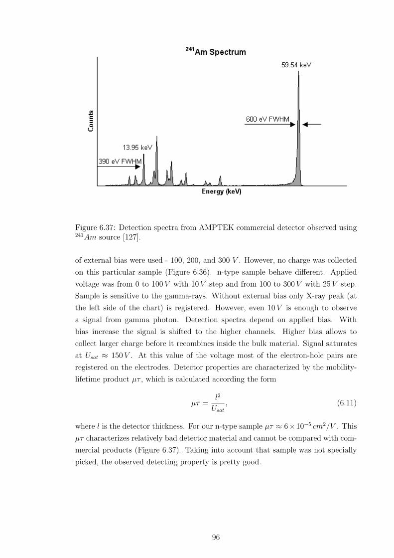
Figure 6.37: Detection spectra from AMPTEK commercial detector observed using241Am source [127].
of external bias were used - 100, 200, and 300 V . However, no charge was collected
on this particular sample (Figure 6.36). n-type sample behave different. Applied
voltage was from 0 to 100 V with 10 V step and from 100 to 300 V with 25 V step.
Sample is sensitive to the gamma-rays. Without external bias only X-ray peak (at
the left side of the chart) is registered. However, even 10 V is enough to observe
a signal from gamma photon. Detection spectra depend on applied bias. With
bias increase the signal is shifted to the higher channels. Higher bias allows to
collect larger charge before it recombines inside the bulk material. Signal saturates
at Usat ≈ 150 V . At this value of the voltage most of the electron-hole pairs are
registered on the electrodes. Detector properties are characterized by the mobility-
lifetime product µτ , which is calculated according the form
µτ =l2
Usat
, (6.11)
where l is the detector thickness. For our n-type sample µτ ≈ 6×10⁻⁵ cm2/V . This
µτ characterizes relatively bad detector material and cannot be compared with com-
mercial products (Figure 6.37). Taking into account that sample was not specially
picked, the observed detecting property is pretty good.
96

Conclusions
The aim of this work was to perform a complex investigation of semi-insulating
CdTe for the gamma ray detector application starting from the crystal growth and
finishing with device characterization.
In-situ high temperature measurements of Hall effect and conductivity were
made on SI CdTe. Surface treatments in non-standard etching solutions was done.
Properties of various contacts fabricated on such surfaces were investigated by the
current-voltage measurements and compared mutually. Capacitance-voltage depen-
dencies for the contacts were collected as well. Finally detection spectra were mea-
sured on the self-made detector. Additional techniques were used in parallel to have
constant control on various samples’ properties.
The main results of the work are:
• Transport properties in SI Cl-doped CdTe at high temperatures were studied.
The chemical diffusion coefficient for the chlorine doped CdTe was established.
• Activation energy of diffusion 2.55 eV in CdTe:Cl was found to be significantly
larger relatively to 1.15 eV in undoped CdTe.
• In compensated CdTe:Cl the densities of the principal point defects change
only weakly and Cl+Te are compensated by A− and V 2−Cd acceptors.
• The proximity of σ relaxed after PCd up/down step proved that there is no
effect of the step direction.
• Experimental set-up for current-voltage measurements on semi-insulating sam-
ples was build. Sophisticated data acquisition software was developed espe-
cially for the new set-up.
• The overall inspection of results allows us to conclude that the best contacts on
n-type SI CdTe are prepared with In deposited thermally on the surface treated
in HI-solution. On p-type SI CdTe the best option results in Au deposited
chemically on the surface treated in HBr-solution. The comparison of the
contact quality relevant to n-type/p-type SI CdTe proves the importance of
well-known type of the conductivity to the choice of proper contact preparation
treatment.
97

• In view of the fact that the treatment in HI-solution with In contact depo-
sition improves/corrupts the quality of the contact on n-type/p-type, we can
conclude that the treatment in HI-solution produces a donor-like (electron-
rich) interface layer, which properly links the n-type with In having low work
function. On the p-type, oppositely, the potential barrier is enhanced and the
contact quality is worse.
• Analogous finding can be deduced for the treatment in HBr-solution where
the formation of an acceptor-like (electron-pure) interface is expected.
• The measurement of current-voltage characteristics on n-type SI CdTe under
forward bias displays in most cases an anomalous concave form, which is not
predicted by standard theories reviewed in textbooks. For the explanation of
that effect we suggest two models: a) trap-mediated transport across barrier;
b) extended depletion of CdTe bulk.
• Theory of the interface traps distributed in the semiconductor band-gap was
successfully used to explain capacitance-voltage measurements.
• Gamma ray spectra measured on the self-made detector showed that our sam-
ples are capable to detect even using low external bias (10 V ).
In future continuation of the research high-temperature electrical measurements
should be made in wider temperature and pressure intervals. Both chlorine and
indium crystals with different degree of doping should be used. Noise measurements
should be applied for the study of the quality of the contacts. Also temperature
dependences of the contacts properties should be investigated. Capacitance mea-
surements at applied voltage up to 100 V should be performed.
98

References
[1] K. Abbas, G. Nicolaou, D. Pellottiero, P. Schwalbach, and L. Koch, Nucl.Instrum. and Methods, vol. A376, p. 248, 1996.
[2] R.B. James, T.E. Schlesinger, J. Lund, and M. Schieber, CdTe Nuclear De-tectors and Applications, vol. 43 of Semiconductors and Semimetals, p. 606,New York: Academic Press, 1995.
[3] M. Cuzin, F. Glasser, R. Mermet, N. Meunier, O.C. Peyret, and P. Rambaud,Proc. SPIE, vol. 2278, p. 21, 1994.
[4] C. Szeles, Phys. Stat. Sol. B, vol. 241, p. 783, 2004.
[5] R. Grill, J. Franc, P. Hoschl, I. Turkevych, E. Belas, and P. Moravec, IEEETrans. Nucl. Sci., vol. 52, p. 1925, 2005.
[6] C. Scharager, P. Siffert, P. Hoschl, P. Moravec, and M. Vanecek, Phys. Stat.Sol. A, vol. 66, p. 87, 1981.
[7] S.A. Medvedev, Yu.V. Klevkov, K.V. Kiseleva, and N.N. Sentyurina, Inorg.Mater., vol. 8, p. 1064, 1972.
[8] M. Wienecke, H. Bereger, and M. Schenk, Mater. Sci. Eng. B, vol. 16, p. 219,1993.
[9] M.L. Cohen and J.R. Chelikowsky, Electronic Structure and Optical Propertiesof Semiconductors, New York: Springer, 1988.
[10] R.F. Brebrick and R. Fang, J. Phys. Chem. Solids, vol. 57, p. 451, 1996.
[11] D. de Nobel, Philips Res. Repts., vol. 14, p. 361, 1959.
[12] J.B. Mullin and B.W. Straughan, Rev. Phys. Appl., vol. 12, p. 105, 1977.
[13] H.M. Hobgood, B.W. Swanson, and R.N. Thomas, J. Cryst. Growth, vol. 85,p. 510, 1987.
[14] H. Yamashita and S. Ibuki, J. Phys. Soc. Jpn., vol. 13, p. 226, 1958.
[15] W.W. Piper and S.J. Polich, J. Appl. Phys., vol. 32, p. 1278, 1961.
[16] K. Zanio, Cadmium Telluride, vol. 13 of Semiconductors and Semimetals,Orlando: Academic Press, 1978.
[17] P. Cheuvart, U. El-Hanani, D. Schneider, and R. Triboulet, J. Cryst. Growth,vol. 101, p. 270, 1990.
99
[18] P. Brunet, A. Katty, D. Schneider, A.Tromsoncarli, and R. Triboulet, Mat.Sci. and Eng. B, vol. 16, p. 44, 1993.
[19] F.A. Kroger, The Chemistry of Imperfect Crystals, vol. 195, New York: Amer-ican Elsevier Comp., 1973.
[20] M.A. Berding, Phys. Rev. B, vol. 60, p. 8943, 1999.
[21] R. Grill, J. Franc, P. Hoschl, I. Turkevych, E. Belas, P. Moravec, M. Fiederle,and K. W. Benz, IEEE Trans. Nucl. Sci., vol. 49, p. 1270, 2002.
[22] P. Emanuelsson, P. Omling, B.K. Meyer, M. Wienecke, and M. Schenk, Phys.Rev. B, vol. 47, p. 15578, 1993.
[23] M.A. Berding, M. van Schilfgaarde, and A. Sher, Phys. Rev. B, vol. 50, p.1519, 1994.
[24] D.M. Hofmann, P. Omling, and H.G. Grimmeiss, Phys. Rev. B, vol. 45, p.6247, 1992.
[25] S.S. Chern, H.R. Vydyanath, and F.A. Kroger, J.Sol.State Chem., vol. 14, p.33, 1975.
[26] S.S. Devlin, Phisics and Chemistry of of II-VI Compounds, Amsterdam:North-Holland, 1967.
[27] D.L. Rode, Phys. Rev. B, vol. 2, p. 4036, 1970.
[28] D. Kranzer, Phys. Stat. Sol. A, vol. 26, p. 11, 1974.
[29] B. Segall, M.R. Lorenz, and R.E. Halsted, Phys. Rev., vol. 129, p. 2471, 1963.
[30] S. Yamada, J. Phys. Soc. Japan, vol. 15, p. 1940, 1960.
[31] I. Turkevych, R. Grill, J. Franc, E. Belasand P. Hoschl, and P Moravec, Semi-cond. Sci. Technol., vol. 17, p. 1064, 2002.
[32] F.T.J. Smith, Trans. Metall. Soc., vol. 1, p. 617, 1970.
[33] J. Franc, R. Grill, L. Turjanska, P. Hoschl, E. Belas, and P. Moravec, J. Appl.Phys., vol. 89, p. 786, 2001.
[34] F. Low and D. Pines, Phys. Rev., vol. 98, p. 414, 1955.
[35] L. Darken, Trans. Inst. Min. Metall., vol. 175, p. 184, 1948.
[36] S.S. Chern and F.A. Kroger, J.Sol.State Chem., vol. 14, p. 44, 1975.
[37] R.C. Whelan and D. Shaw, Phys. Status Solidi B, vol. 29, p. 145, 1968.
[38] K.R. Zanio, Appl. Phys. Lett., vol. 15, p. 260, 1969.
[39] Yu.V. Rud’ and K.V. Sanin, Soviet Phys. Semicond., vol. 5, p. 244, 1969.
[40] K.R. Zanio, J. Appl. Phys., vol. 41, p. 1935, 1970.
[41] Yu.V. Rud’ and K.V. Sanin, Soviet Phys. Semicond., vol. 6, p. 764, 1972.
100

[42] Yu.V. Rud and K.V. Sanin, Inorg. Mater., vol. 10, p. 839, 1974.
[43] S.S. Chern and F.A. Kroger, J.Sol.State Chem., vol. 14, p. 299, 1975.
[44] H.H. Woodbury, Phys. Rev., vol. 134, p. A492, 1964.
[45] P.M. Borsenberger, D. Stevenson, and R.A. Burmeister, II-VI SemiconductingCompound, International Conference, New York: W. A. Benjamin, Inc., p.439, 1967.
[46] R.C. Whelan and D. Shaw, II-VI Semicond. Comp., p. 451, 1967.
[47] H.H. Woodbury and R.B. Hall, Phys. Rev., vol. 157, p. 641, 1967.
[48] D.A. Stevenson, In: D.S. Shaw, Editor, Atomic Diffusion in Semiconductors,Plenum, London, p. 494, 1973.
[49] P.M. Borsenberger and D.A. Stevenson, J. Phys. Chem. Solids, vol. 29, p.1277, 1968.
[50] R. Grill, E. Belas, M. Bugar, P. Hoschl, B. Nahlovskyy, P. Fochuk, O. Panchuk,A. E. Bolotnikov, and R. B. James, IEEE Trans. Nucl. Sci., vol. 56, p. 1763,2009.
[51] R. Grill, E. Belas, J. Franc, P. Hoschl, and P. Moravec, Nucl. Instr. andMethods, vol. A591, p. 218, 2008.
[52] D.R. Lide, Ed., CRC HadNicollianbook of Chemistry and Physics, CRC Press,Boca Raton, FL, 1998.
[53] C. Debiemme-Chouvy, F. Iranzo Marin, U. Roll, M. Bujor, and A. Etcheberry,Surf. Sci., vol. 352, p. 495, 1996.
[54] D.A. Slater, Y. Luo, and R.M. Osgood Jr., J. Cryst. Growth, vol. 159, p. 754,1996.
[55] I.M. Dharmadasa, Prog. Cryst. Growth Charact. Mater., vol. 39, p. 249, 1998.
[56] F.X. Wagner and D. Sands, Thin Solid Films, vol. 358, p. 6, 2000.
[57] J.P. Ponpon, Solid-State Electron., vol. 28, p. 689, 1985.
[58] Y. Eisen, Nucl. Instrum. and Methods, vol. A380, p. 431, 1996.
[59] D. Rose, K. Durose, W. Paloszand, A. Szczerbakow, and K. Grasza, J. Phys.D: Appl. Phys., vol. 31, p. 1009, 1998.
[60] Daniel Lincot and Jacques Vedel, J. Electroanal. Chem., vol. 175, p. 207, 1984.
[61] D. Landolt, Electrochim. Acta, vol. 32, p. 1, 1987.
[62] P.M. Amirtharaj and Fred H. Pollak, Appl. Phys. Lett., vol. 45, p. 789, 1984.
[63] M. Saji and N. Kondon, Oyo Butsuri, vol. 54, p. 835, 1985.
[64] T. Ozaki, Y. Iwase, H. Takamura, and M. Ohmori, Nucl. Instrum. and Meth-ods, vol. A380, p. 141, 1996.
101
[65] H. Cordes and R. Schmid-Fetzer, Semicond. Sci. Technol., vol. 9, p. 2085,1994.
[66] A. Szczerbakow, J. Domagala, D. Rose, K. Durose, V.Yu. Ivanov, and A.R.Omeltchouk, J. Cryst. Growth, vol. 191, p. 673, 1998.
[67] I.M. Dharmadasa, A.B. McLean, M.H. Patterson, and R.H. Williams, Semi-cond. Sci. Technol., vol. 2, p. 404, 1987.
[68] B. Daudin, D. Brun-Le Cunff, and S. Tatarenko, Surf. Sci., vol. 352, p. 99,1996.
[69] D.E. Aspnes and H. Arwin, J. Vac. Sci. Technol., A, vol. 2, p. 1309, 1984.
[70] U. Sassenberg, H. Berger, and A. Engel, Cryst. Res. Technol., vol. 22, p. K86,1987.
[71] J.P. Ponpon, Appl. Phys. A, vol. 27, p. 11, 1982.
[72] M. Hage-Ali, R. Stuck, A.N. Saxena, and P. Siffert, Appl. Phys. A, vol. 19, p.25, 1979.
[73] D.L. Batzner, R. Wendt, A. Romeo, H. Zogg, and A.N. Tiwari, Thin SolidFilms, vol. 361, p. 463, 2000.
[74] W.J. Danaher, L.E. Lyons, M. Marychurch, and G.C. Morris, Appl. Surf. Sci.,vol. 27, p. 338, 1986.
[75] W.H. Chang, T. Lee, and W.M. Lau, J. Appl. Phys., vol. 68, p. 4816, 1990.
[76] Z. Sobiesierski, I.M. Dharmadasa, and R.H. Williams, Appl. Phys. Lett., vol.53, p. 2623, 1988.
[77] Y. Luo, D.A. Slater, M. Levy, and R.M. Osgood Jr., Appl. Surf. Sci., vol. 104,p. 49, 1996.
[78] H. Yoon, J.M. VanScyoc, and M.S Goorsky, J. Electron. Mater., vol. 26, p.529, 1997.
[79] M.S. Han and T.W. Kang amd T.W. Kim, Appl. Surf. Sci., vol. 148, p. 105,1999.
[80] L. Wang, W. Sang, W. Shi, Y. Qian, J. Min, D. Liu, and Y. Xia, Nucl.Instrum. and Methods, vol. A448, p. 581, 2000.
[81] A. Burger, H. Chen, K. Chattopadhyay, D. Shi, S.H. Morgan, W.E. Collins,and R.B. James, Nucl. Instrum. Methods Phys. Res., Sect. A, vol. 428, p. 8,1999.
[82] P.J. Ireland, Thin Solid Films, vol. 304, p. 1, 1997.
[83] O.S. Galkina, N.N. Grebenyuk, M.V. Dobrotvorskaya, V.K. Komar, and D.P.Nalivaiko, Funct. Mat., vol. 8, p. 392, 2001.
[84] A.J. Fusco and B.C. Cochran, “Method for polishing detector material,” Pat.USA # 4600469.
102

[85] P.W. Leech, P.J. Gwynn, and M.H. Kibel, Appl. Surf. Sci., vol. 37, p. 291,1989.
[86] P.W. Leech, M.H. Kibel, and P.J. Gwynn, J. Electrochem. Soc., vol. 137, p.705, 1990.
[87] G.N. Pain, N. Bharatula, T.J. Elms, P. Gwynn, M. Kibel, M.S. Kwietniak,P. Leech, N. Petkovic, C. Sandford, J. Thompson, T. Warminski, D. Gao, S.R.Glanvill, C.J. Rossouw, and A.W. Stevenson, J. Vac. Sci. Technol., A, vol. 8,p. 1067, 1990.
[88] O.S. Galkina, N.N. Grebenyuk, M.V. Dobrotvorskaya, V.K. Komar, D.P. Nali-vaiko, and O.N. Chugai, Funct. Mat., vol. 9, p. 463, 2002.
[89] Z.F. Tomashik, O.R. Gumenyuk, and V.N. Tomashik, Proc. SPIE, vol. 5065,p. 241, 2003.
[90] W. Kern, RCA Rev., vol. 39, p. 278, 1978.
[91] B. Schwartz and H. Robbins, J. Electrochem. Soc., vol. 111, p. 196, 1964.
[92] B. Schwartz and H. Robbins, J. Electrochem. Soc., vol. 123, p. 1903, 1976.
[93] R.N. Zitter, Surf. Sci., vol. 28, p. 335, 1971.
[94] M.H. Patterson and R.H. Williams, J. Phys. D: Appl. Phys., vol. 11, p. L83,1978.
[95] A.J. Ricco, H.S. White, and M.S. Wrighton, J. Vac. Sci. Technol., A, vol. 2,p. 910, 1984.
[96] P. Gaugash and A.G. Milnes, J. Electrochem. Soc., vol. 128, p. 924, 1981.
[97] H.C. Montgomery, Solid-State Electron., vol. 7, p. 147, 1964.
[98] I. Hahnert and M. Wienecke, Mater. Sci. Eng., B, vol. 16, p. 168, 1993.
[99] L.E. Lyons, G.C. Morris, N.A. Raftery, and T.L. Young, Aust. J. Chem., vol.40, p. 655, 1987.
[100] M. Inoue, I. Teramoto, and S. Takayanagi, J. Appl. Phys., vol. 33, p. 2578,1962.
[101] W. Faschinger, K. Lischka, and H. Sitter, Chemtron., vol. 2, p. 28, 1987.
[102] Y.-C. Lu, C.M. Stahle, R.S. Feigelson, and J. Morimoto, J. Appl. Phys., vol.62, p. 4453, 1987.
[103] K. Chattopadhyay, S. Feth, H. Chen, A. Burger, and Ching-Hua Su, J. Cryst.Growth, vol. 191, p. 377, 1998.
[104] B.J. Kowalski, B.A. Orowski, and J. Ghijsen, Surf. Sci., vol. 412, p. 544, 1998.
[105] T. Takeuchi, T. Kore-eda, and A. Ebina, Appl. Surf. Sci., vol. 100, p. 596,1996.
103

[106] S.C. Gupta, F.R. Chavada, S.K. Koul, and M. Gautanam, J. Electrochem.Soc., vol. 135, p. 2899, 1988.
[107] B. Wermke, M. Muhlberg, A. Engel, and P. Rudolph, Cryst. Res. Technol.,vol. 24, p. 365, 1989.
[108] K. Nakagawa, K. Maeda, and S. Takeuchi, Appl. Phys. Lett., vol. 34, p. 574,1979.
[109] S. Zhu, B. Zhao, Q. Li, F. Yu, S. Shao, and X. Zhu, J. Cryst. Growth, vol.208, p. 264, 2000.
[110] http://www.nikko-metal.co.jp/products/05 kagou/pdf/puremetal.pdf
[111] L. Turjanska, P. Hoschl, E. Belas, R. Grill, J. Franc, and P. Moravec, Nucl.Instr. Methods A, vol. 90, p. 458, 2001.
[112] L.J. van der Pauw, Phillips Res. Repts, vol. 13, p. 1, 1958.
[113] L.J. van der Pauw, Phillips Tech. Rev., vol. 20, p. 220, 1958.
[114] R.Grill, L.Turjanska, J.Franc, E.Belas, I.Turkevych, and P.Hoschl, Phys. Stat.Sol. B, vol. 229, p. 161, 2002.
[115] A.M. Goodman, J. Appl. Phys., vol. 34, p. 329, 1963.
[116] R. Stibal, J. Windscheif, and W. Jantz, Semicond. Sci. Technol., vol. 6, p.995, 1991.
[117] P. Fochuk, O. Panchuk, L. Shcherbak, and P. Siffert, Phys. Stat. Sol. C, vol.2, p. 1178, 2005.
[118] M.U. Ahmed and E.D. Jones, EMIS Datareviews Series No. 10, chapter B4.2,p. 466, INSPEC, London, January 1994.
[119] S.H. Wei and S.B. Zhang, Phys. Rev. B, vol. 66, p. 155211, 2002.
[120] W. Shockley and W.T. Read, Phys. Rev., vol. 87, 1952.
[121] J.W. Mayer, Semiconductor Detectors, p. 445, North Holland, Amsterdam,1968.
[122] C. Szeles, Y.Y. Shan, K.G. Lynn, and E.E. Eissler, Nucl. Instr. and Methods,vol. A380, p. 148, 1996.
[123] A. Castaldini, A. Cavallini, B. Fraboni, P. Fernandez, and J. Piqueras, J.Appl. Phys., vol. 83, p. 2121, 1998.
[124] H. Elhadidy, J. Franc, P. Moravec, P. Hoschl, and M. Fiederle, Semicond. Sci.Technol., vol. 22, p. 537, 2007.
[125] J. Franc, R. Grill, J. Kubat, P. Hlıdek, E. Belas, P. Moravec, and P. Hoschl,J. Electron. Mater., vol. 35, p. 988, 2006.
[126] E.H. Nicollian and J.R. Brews, MOS (Metal-Oxide-Semiconductor) Physicsand Technology, Wiley, New York, 1982.
[127] http://www.amptek.com/cdte.html
104