semicond cto ssemiconductorss3.amazonaws.com/noteswap-sid-1/7/2/d/b/72db72a9b6... · charge. it has...
TRANSCRIPT

Semicond cto sSemiconductors
Crystalline solid materials whose resistivities are values between those of conductors and insulatorsinsulators.Good electrical characteristics and feasible fabrication technology are some reasons why gy ysilicon is by far the most important semiconductor material in use today.C d i d t t i l hCompound semiconductor materials such as gallium arsenide are used in photonic and microwave applications, and germanium ismicrowave applications, and germanium is used for a few special purposes.

Semicond cto sSemiconductors
Silicon atoms join together to form a regular three dimensional structure called a crystal lattice.Pure semiconductor materials, termed u e se co ducto ate a s, te edintrinsic semiconductors, are neutral in total charge and are also a poor tota c a ge a d a e a so a pooconductor of electricity. This means they have very few charge carriers. y y g

Int insic Semicond ctoIntrinsic Semiconductor
DopingDoping
Process that adds a small amounts of impurities, dopants, to a semiconductor, so that it can be made to contain a desiredthat it can be made to contain a desired number of either holes or free electrons.After the doping process the materials p g pgenerated are termed extrinsic semiconductors. They are impure.I iti l ifi d ithImpurities are classified as either:
Donor.AcceptorAcceptor.

E t insic Semicond cto sExtrinsic Semiconductors
Donor impurities donate extra electrons to the silicon lattice:
Antimony, Arsenic and Phosphorus.
They have 5 electrons in their outer electron shell Four of them will be used in theshell. Four of them will be used in the covalent bonds to the neighboring silicon atoms but the fifth can be easily freed fromatoms, but the fifth can be easily freed from their original atoms by thermal energy even at room temperatures.p

N T pe Semicond ctoN-Type Semiconductor
Semiconductor materials doped to contain excess free electrons are considered n-type
i d tsemiconductors.Even though the added impurity created excess free electrons the material is stillexcess free electrons, the material is still neutral in charge.It has been found that in n type materials theIt has been found that in n-type materials the free electron concentration is approximately equal to the donor atom doping density:equal to the donor atom doping density:
n ≈ ND

N T pe Semicond ctoN-Type Semiconductor

E t insic Semicond cto sExtrinsic Semiconductors
Acceptor impurities create a hole in the silicon lattice:
Boron, Gallium and Indium.
They have 3 electrons in their outerThey have 3 electrons in their outer electron shell, and they are not enough to fill all the orbitals around it. Thisto fill all the orbitals around it. This leaves a bond site empty, and this empty place is called a hole.empty place is called a hole.

P T pe Semicond ctoP-Type Semiconductor
Semiconductor materials doped to contain excess holes are considered p-typesemiconductorssemiconductors.Even though the added impurity created excess holes, the material is still neutral in ,charge.It has been found that in p-type materials the h l t ti i i t l l thole concentration is approximately equal to the donor atom doping density:
p ≈ Np ≈ NA

P T pe Semicond ctoP-Type Semiconductor

Semicond cto sSemiconductors
Extrinsic semiconductors can be doped with both types of impurities, and their respective concentrations determine the type materialconcentrations determine the type material they will become:
N-type when ND > NA
Majority carriers are free electrons and minority carriers are holes.
P-type when ND < NAP type when ND < NA
Majority carriers are holes and minority carriers are free electrons.

Semicond cto sSemiconductors
In pure, intrinsic, semiconductors free electrons and holes are created in pairs; therefore the intrinsic carrier concentration is defined as:
ni = n = pFor silicon at 300°K,For silicon at 300 K,
ni ≈ 1.6 X 10¹⁰ electrons/cm3

Current Conduction in Semicond cto sSemiconductors
At temperatures above absolute zero the free carriers are in constant random motion due to th i th l h th i ttheir thermal energy, however their net motion in any particular direction is zero, therefore there is no net current flowtherefore there is no net current flow.
Current Conduction in Semicond cto sSemiconductors
There are two principle mechanisms by which charge move in a particular direction, thus creating an electric current:
Drift.Diffusion.

D iftDrift
Applying an electric field across a semiconductor material, results in both types of carrier moving in opposite directions thus creating current flow.

D iftDrift
The magnitude of the electric field in volts/cm is given by:
V
And the effective velocity of the carrier moving byLV
=E
And the effective velocity of the carrier moving by the drift action of an applied electric filed is given by:
Ev μ= Ev μ=
Where μn = 1350 cm2/V-s and μp = 480 cm2/V-s are the electron and hole mobility constants respectively
Ennv μ= Eppv μ=
the electron and hole mobility constants respectively.

Cond cti itConductivity
Property of a material.It is a measure of the material’s abilityIt is a measure of the material s ability to to carry electric current.It is given by:It is given by:
( )pn pnq μμσ +=
Measured in S/m.
( )p

Resisti itResistivity
Measured in Ω-m it is the reciprocal of conductivity:
σρ 1=
The resistance of a material with constant cross section can be calculated by:
ALR ρ=

C ent DensitCurrent Density
Current per unit cross-sectional area.Measured in A/cm2.Given by:
EJ σ=The direction of current flow vector is the
EJ σ=
same direction as the electric field vector.

Diff sionDiffusion
Diffusion current occurs because of the physical principle that over time particles
d i d ti ill hundergoing random motion will show a movement from a region of high concentration to a region of lowerconcentration to a region of lower concentration.

Diff sionDiffusion
⎤⎡ ⎤⎡⎥⎦⎤
⎢⎣⎡=dxdnqDJ nn ⎥⎦
⎤⎢⎣⎡=dxdpqDJ pp
Current density is directly proportional to the
⎦⎣ ⎦⎣
gradient of carrier concentration.Dn and Dp are the diffusion constants for pelectrons and holes respectively.
DiodesDiodes
A two terminal electronic device which conducts current if a voltage source is applied i di ti d f t d tin one direction, and refuses to conduct significant current when a voltage of opposite polarity is appliedpolarity is applied.A diode is said to be forward biased when it is conducting current and it is said to beis conducting current, and it is said to be reversed biased when it is not conducting significant current.g

DiodesDiodes
It is a non-linear device.It is represented by the followingIt is represented by the following symbol, where the arrow indicates the direction of positive current flow.d ect o o pos t e cu e t o

DiodesDiodes
Historical perspective:Vacuum tube diode, Cat’s whisker.,
Modern devices:p-n junction diode Schottky diode Zenerp n junction diode, Schottky diode, Zener diode, Tunnel diode, Varactor, etc.
P N J nctionP-N Junction
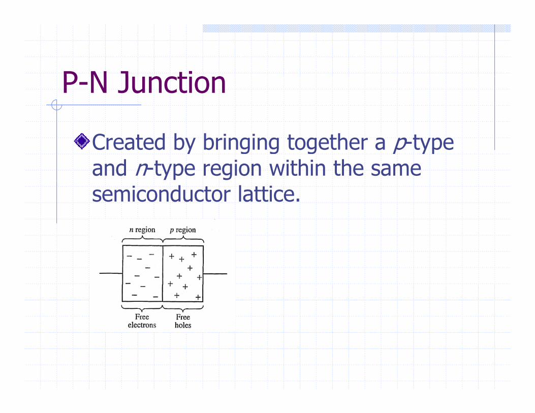
Created by bringing together a p-type and n-type region within the same semiconductor lattice.

P N J nctionP-N Junction
At the instant this junction is created free electrons and holes start diffusing from their
i f hi h t ti t i fregions of high concentration to regions of low concentration.This diffusion process is stopped very quicklyThis diffusion process is stopped very quickly due to the fact that the movement of the free electrons and holes leave behind uncoveredelectrons and holes leave behind uncovered negative and positive charges bound in the lattice (dopant atoms).( p )

Depletion RegionDepletion Region
This process builds up charge layers in
i ll da region, called depletion region, which is depleted ofwhich is depleted of carriers.The charge layerThe charge layer prevents further diffusion.
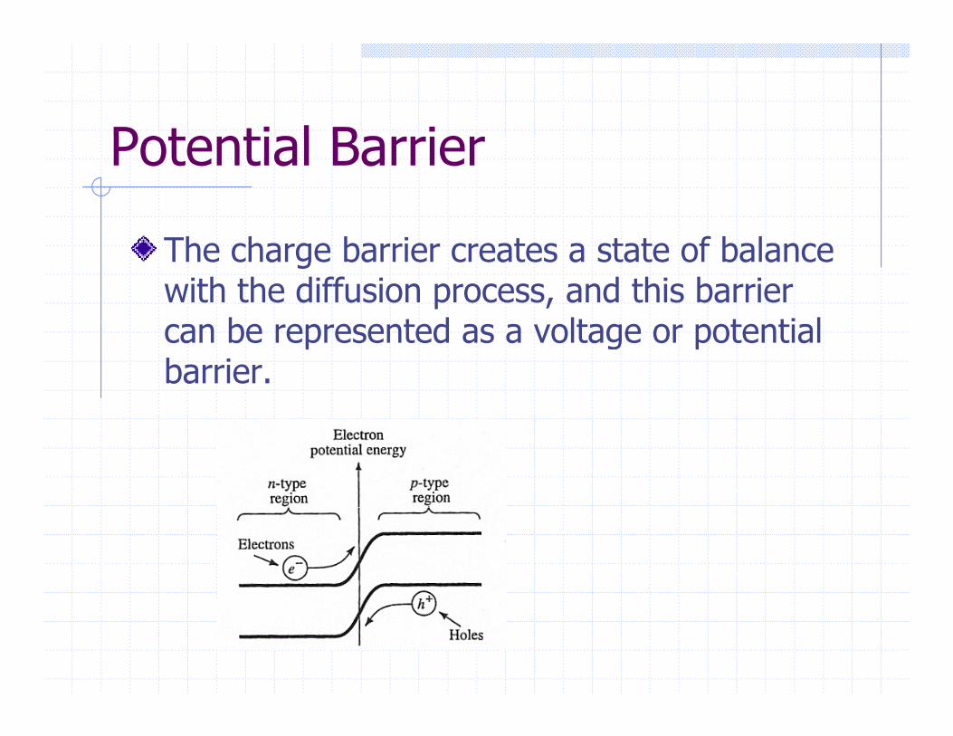
Potential Ba iePotential Barrier
The charge barrier creates a state of balance with the diffusion process, and this barrier
b t d lt t ti lcan be represented as a voltage or potential barrier.

Potential Ba iePotential Barrier
Note that the height of the potential barrier across the p-n junction can be
difi d b l i t lmodified by applying an external voltage across the junction.Th diff i f i thThe diffusion of carriers across the junction is exponentially related to the barrier height:barrier height:
Change in voltage incurs an exponential change in current due to carrier diffusion.change in current due to carrier diffusion.

Potential Ba iePotential Barrier
If the p-region is made more positive than the n-region then the height of barrier is
d d d i diffreduced and more carriers can diffuse through junction. This is called forward bias.

Potential Ba iePotential Barrier
If the p-region is made more negative than the n-region then the height of barrier is i d d f i diffincreased and very few carriers can diffuse through junction. This is called reverse bias.

T n on VoltageTurn-on Voltage
Is arbitrarily defined by some manufacturers to be the externally applied voltage (forward bias) required to obtain 1 μA of current flow.It is designated by VF

Diode Ci c it ModelsDiode Circuit Models
Diode models that predict the relation between the dc voltage across the diode, VD ,
d th t th h th di d Iand the current through the diode, ID , are used to analyze circuits containing this non-linear device Three models will be discussedlinear device. Three models will be discussed here:
The ideal diode model;;The diode equation model;The piecewise linear diode model.

Diode Ci c it ModelsDiode Circuit Models
Which model should you use?Ask yourself:Ask yourself:
What do I know about the problem?Which is the simplest model that will giveWhich is the simplest model that will give me results with accuracy I desire?

Ideal DiodeIdeal Diode
d l d lIdealized two terminal device which passes current in one direction (zero resistance) and(zero resistance) and passes no current in the opposite direction (infinite resistance).(infinite resistance).Its v-i plot, which shows the relationship of the voltage across the diode gand the current flowing through it, contains a discontinuity.

Ideal DiodeIdeal Diode
If the diode is forward biased then the ideal diode conducts current as a closed switch.If the diode is reverse biased then the ideal diode willIf the diode is reverse biased then the ideal diode will not conduct current, and it will appear as an open switch.
Ideal DiodeIdeal Diode
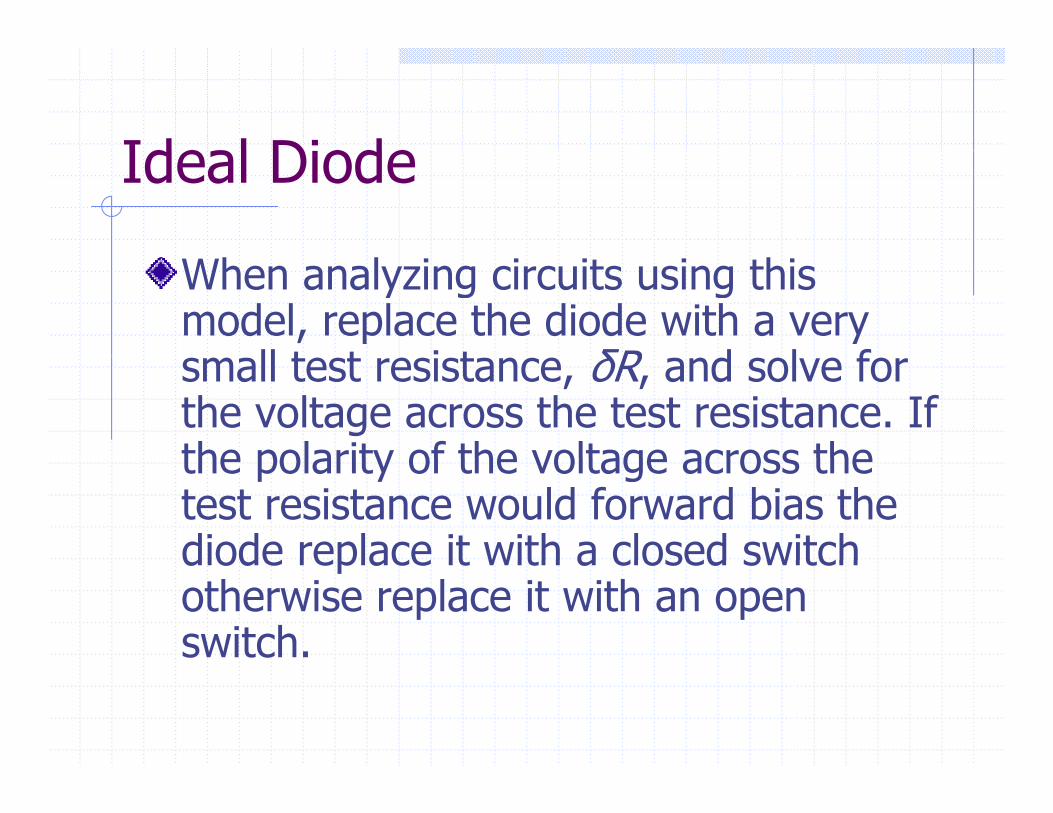
When analyzing circuits using this model, replace the diode with a very
ll t t i t δR d l fsmall test resistance, δR, and solve for the voltage across the test resistance. If the polarity of the voltage across thethe polarity of the voltage across the test resistance would forward bias the diode replace it with a closed switchdiode replace it with a closed switch otherwise replace it with an open switch.
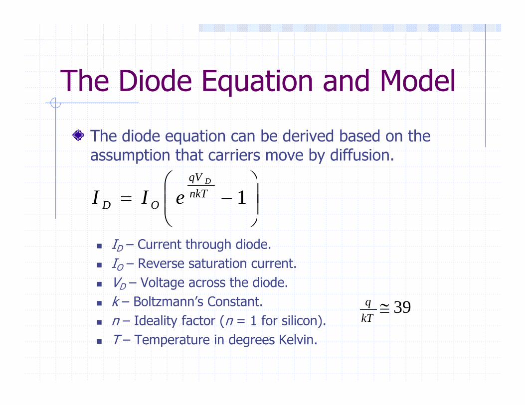
The Diode Eq ation and ModelThe Diode Equation and Model
The diode equation can be derived based on the assumption that carriers move by diffusion.
⎞⎛ qV
⎟⎟⎠
⎞⎜⎜⎝
⎛−= 1nkT
qV
OD
D
eII
ID – Current through diode.IO – Reverse saturation current.V V lt th di dVD – Voltage across the diode.k – Boltzmann’s Constant.n – Ideality factor (n = 1 for silicon).
39≅kTq
T – Temperature in degrees Kelvin.

The Diode Eq ation and ModelThe Diode Equation and Model
⎟⎟⎠
⎞⎜⎜⎝
⎛−= 1nkT
qV
OD
D
eII ⎟⎠
⎜⎝
O

G aphical Sol tionGraphical Solution
Simplify the circuit connected to the diode to a Thevenin’s equivalent circuit. Analyze two cases:
iD = 0;D ;vD = 0.
This two points identifies the Thevenin’sidentifies the Thevenin s circuit load line, and this lines intersects the diode plot at thediode plot at the operating point.

Piece ise Linea ModelPiecewise Linear Model
The real diode can be approximated by a model which usesa model which uses two connected line segments.Note that the turn on voltage, VF , marks the pointmarks the point where the two line segments meet.g

Po e S ppl Ci c itsPower Supply Circuits
Power supply circuits are used to convert ac to dc for the purpose of operating electronic circuits.Typical residential ac power yp ca es de t a ac po edistribution:
110-120 volts;110 120 volts;220-240 volts.
Po e S ppl Ci c itsPower Supply Circuits
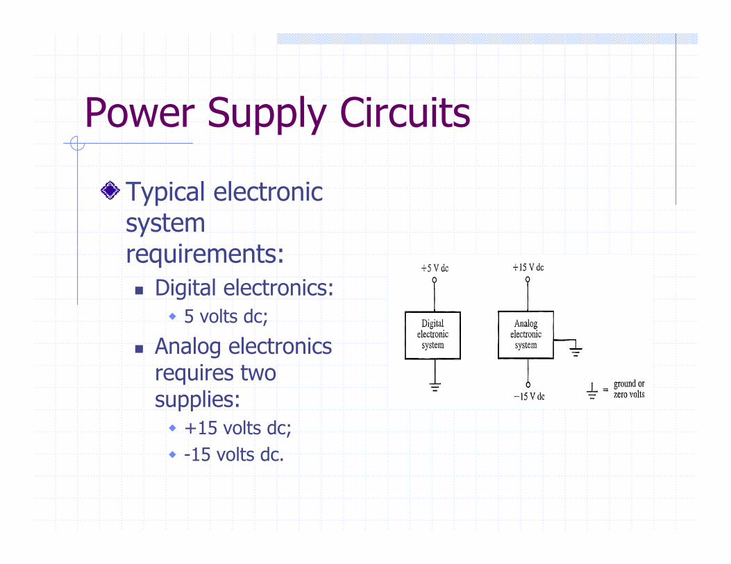
Typical electronic system
i trequirements:Digital electronics:
5 volts dc;5 volts dc;
Analog electronics requires two supplies:
+15 volts dc;-15 volts dc.15 volts dc.

Po e S ppl Ci c itsPower Supply Circuits
To achieve its purpose a power supply must:
Step down the voltage supplied;Convert ac to dc by rectifying the ac.y y g
A transformer is used to step down the magnitude of the voltages from the wallmagnitude of the voltages from the wall receptacle.

T ansfo meTransformer
A transformer consists of two coils of wire on a common iron core. The voltages on these t il l t d b th t ti hi htwo coils are related by the turns ratio, which is the ratio of the number of turns of wire in the secondary coil to that in the primary coilthe secondary coil to that in the primary coil.

RMS Val esRMS Values
Note that the 110-120 volts and 220-240 volts are RMS values.The actual amplitude of that sinusoidal signal is a factor of √2 larger.s g a s a acto o √ a ge

RectificationRectification
Converting ac to dc is accomplished by the process of rectification.Two processes are used:
Half-wave rectification;Half wave rectification;Full-wave rectification.

Half a e RectificationHalf-wave Rectification
Simplest process used to convert ac t dto dc.A diode is used to clip the input signalclip the input signal excursions of one polarity to zeropolarity to zero.

F ll a e RectificationFull-wave Rectification
The output of a full-wave rectifier is d i b b th thdriven by both the positive and negative cycles ofnegative cycles of the sinusoidal input, unlike the half-wave rectifier which uses only one cycle.

Filte ingFiltering
Process used to smooth out the
t t f thoutput of the rectifier circuit.One of the mostOne of the most common filter is the RC networkRC network.
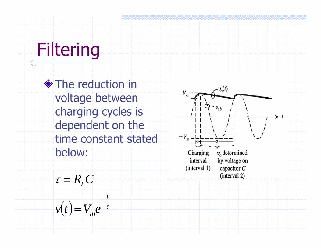
Filte ingFiltering
The reduction in voltage between h i l icharging cycles is
dependent on the time constant statedtime constant stated below:
( )
τt
LCR−
=
( ) τmeVtv =

Ripple FactoRipple Factor
Ripple is the small voltage variation from the filter’s output.Good power supplies produce as little ripple as possible.pp e as poss b eRipple is usually specified as Ripple Factor RF :Factor, RF :
rippleofvaluermsRF =valuedc

Clippe Ci c itsClipper Circuits
Used to limit the voltage excursions f i l tof a signal at some
particular positive value negativevalue, negative value or both.

Clampe Ci c itsClamper Circuits
Used to generate an output waveform which appears likewhich appears like the input one except that the DC level h h h f dhas either shifted positively or negatively withnegatively with respect to the input waveform.

Voltage M ltiplie Ci c itsVoltage Multiplier Circuits
A voltage multiplier is an electrical circuit that converts AC electrical power from a lower voltage to a higher DC voltage bylower voltage to a higher DC voltage by means of capacitors and diodes combined into a network.

Zene DiodeZener Diode
Analyzing a diode operating in the reverse bias region will show that the current through it remains essentially constant until the breakdown voltage alsoessentially constant until the breakdown voltage, also called the avalanche or zener breakdown voltage, is reached. At this point the current will increase very apidl fo a small oltage changerapidly for a small voltage change.

Voltage Reg lationVoltage Regulation
This characteristic of the zener diode is very useful for voltage regulation circuits. The zener diode provides an effective way to clamp or limit the voltage at a relatively constant value thus creating a voltage regulation capability.

Voltage Reg lationVoltage Regulation

Photo Diodes and LEDsPhoto Diodes and LEDs
Photodiodes convert incident radiation to electric current.The sun’s radiation creates electron hole pairsThe sun’s radiation creates electron-hole pairs in the depletion region of a large p-n diode, and the electric field in this region sweeps the g pcarriers to the terminals thus generating current.Th it d f th t i t lThe magnitude of the current approximately proportional to the light incidence on the diode.diode.

Photo Diodes and LEDsPhoto Diodes and LEDs
Light Emitting Diodes – LEDs are p –njunctions fabricated from special semiconductors materials, like gallium arsenide. They are useful because they allow direct recombination of electrons and holes, thus releasing energy in the form of light.