the real hardware - physikalisches institutangelov/vhdl/vhdl_ss09_teil… · propagation delays –...
TRANSCRIPT
© V. Angelov VHDL-FPGA@PI 2013 1
The real hardware
© V. Angelov VHDL-FPGA@PI 2013 2
The real hardware
•
Propagation delays–
worst case, typical case, best case…
–
setup/hold, fMAX
•
Clock tree and timing analysis•
Power consumption
•
Timing of the I/O pins–
I/O vs. internal registers
–
I/O delays, slew rate settings•
Timing simulations
© V. Angelov VHDL-FPGA@PI 2013 3
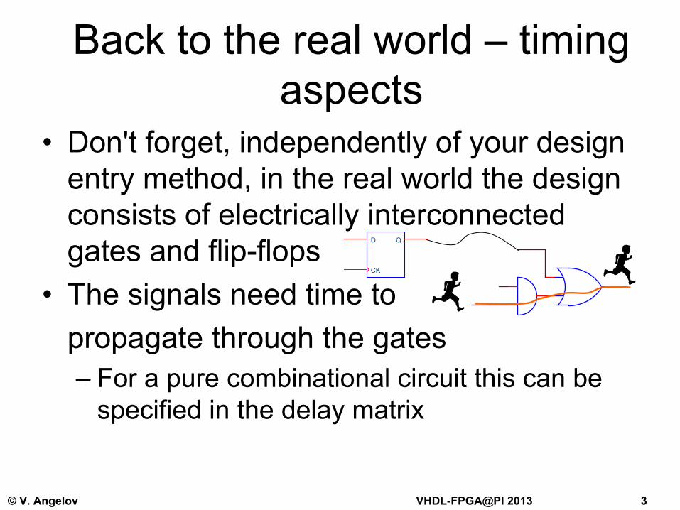
Back to the real world – timing aspects
•
Don't forget, independently of your design entry method, in the real world the design consists of electrically interconnected gates and flip-flops
•
The signals need time topropagate through the gates–
For a pure combinational circuit this can be specified in the delay matrix
D
CK
Q
© V. Angelov VHDL-FPGA@PI 2013 4
Timing aspects – variations (corners)
•
The properties of the logic gates and flip-flops are not constant, unlike the electrons, the real gates aren't perfect clonings!–
Variation inside the same chip
–
Variations chip to chip–
Variations with the temperature (slower at higher temperatures)
–
Variations with the supply voltage (faster at higher voltages)
–
Dependence on the different capacitive load
© V. Angelov VHDL-FPGA@PI 2013 5
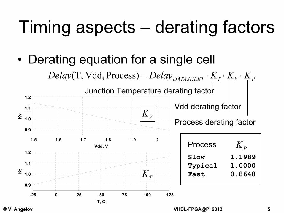
Timing aspects – derating factors
•
Derating
equation for a single cellPVTDATASHEET KKKDelayDelay ⋅⋅⋅=)Process Vdd, T,(
Junction Temperature derating
factor
Vdd
derating
factor
Process derating
factor0.9
1.0
1.1
1.2
1.5 1.6 1.7 1.8 1.9 2
Kv
Vdd, V
0.9
1.0
1.1
1.2
-25 0 25 50 75 100 125
Kt
T, C
TK
VK
Slow 1.1989Typical 1.0000Fast 0.8648
PKProcess
© V. Angelov VHDL-FPGA@PI 2013 6
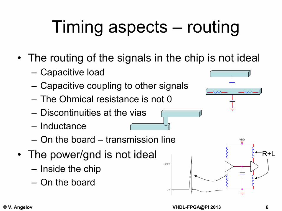
•
The routing of the signals in the chip is not ideal–
Capacitive load
–
Capacitive coupling to other signals–
The Ohmical
resistance is not 0
–
Discontinuities at the vias–
Inductance
–
On the board –
transmission line•
The power/gnd
is not ideal
–
Inside the chip–
On the board
Timing aspects – routing
VDD
0V
10mV
R+L

© V. Angelov VHDL-FPGA@PI 2013 7
Timing aspects – setup/hold
•
The data to the flip-flop inputs must be stable some time before (setup time tSU
) and after (hold time tH
) the active edge of the clock–
If the conditions above are not fulfilled, we speak of timing violations
•
The flip-flop outputs toggle with some delay after the active edge of the clock–
clock to output
© V. Angelov VHDL-FPGA@PI 2013 8
0.2
0.3
0.4
0.5
0.6de
lay,
ns
0.1
0.2
1 2 3 4 5 6 7 8 9 10 11 12 13 14 15 16
Ener
gy, p
J
fanout
Example DFF ASIC cellD
CK
Q
CEB
Static power 89 pWArea 332 μm2Input capacitance
CEB 5.33 fFCK 5.14 fFD 3.70 fF
CEB↓
CK↑
0.161CEB↑
CK↑
0.210
D ↓
CK↑
0.175D ↑
CK↑
0.188
Setup time, nsAll hold times 0
CK↑
Q↑
CK↑
Q↓
min CLK
pulse width 0.25ns
© V. Angelov VHDL-FPGA@PI 2013 9
D
ENA
QPRE
CLR
D
ENA
QPRE
CLR
D
ENA
QPRE
CLR
D
ENA
QPRE
CLR
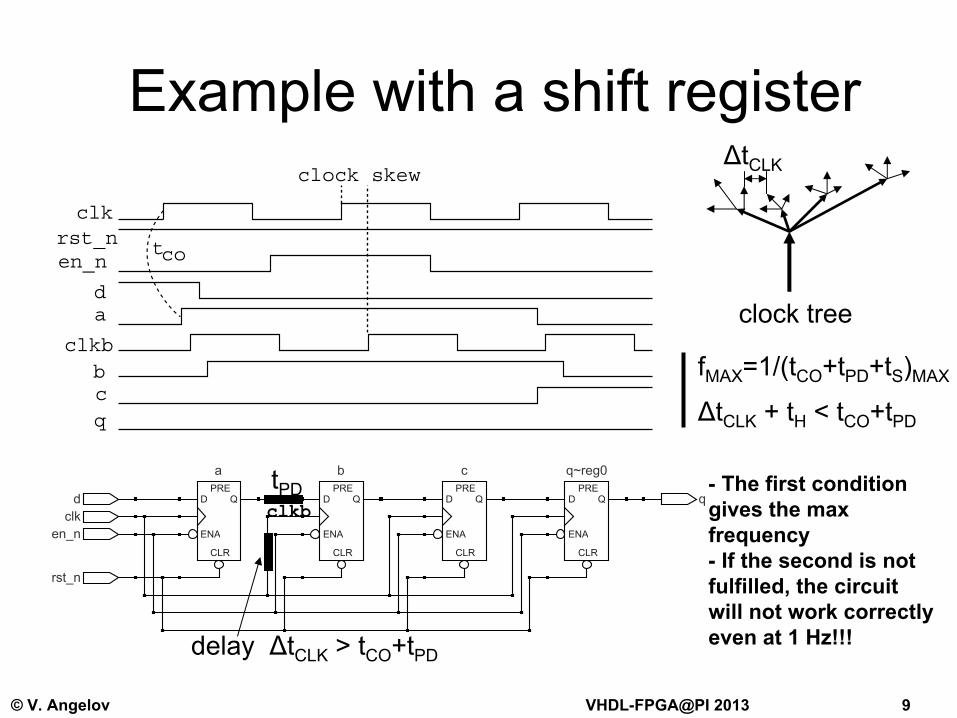
a b c q~reg0
clk
rst_n
en_n
d q
Example with a shift register
clock tree
clkb
delay ∆tCLK
> tCO
+tPD
tPD
fMAX
=1/(tCO
+tPD
+tS
)MAX
∆tCLK
+ tH
< tCO
+tPD
-
The first condition gives the max frequency-
If the second is not fulfilled, the circuit will not work correctly even at 1 Hz!!!
clkrst_n
d
en_n
a
bcq
clkb
tco
clock skew∆tCLK
© V. Angelov VHDL-FPGA@PI 2013 10
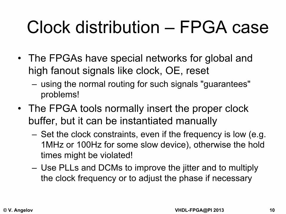
Clock distribution – FPGA case•
The FPGAs
have special networks for global and
high fanout
signals like clock, OE, reset–
using the normal routing for such signals "guarantees" problems!
•
The FPGA tools normally insert the proper clock buffer, but it can be instantiated manually–
Set the clock constraints, even if the frequency is low (e.g. 1MHz or 100Hz for some slow device), otherwise the hold times might be violated!
–
Use PLLs
and DCMs
to improve the jitter and to multiply the clock frequency or to adjust the phase if necessary

© V. Angelov VHDL-FPGA@PI 2013 11
•
Phase-locked loop
–
Zero delay between input and output–
Less jitter at the output
–
Restored clock symmetry
PLL
Phase Detector
Lowpass filter
VCO clock bufferreference clock
Voltage Controlled Oscillator
output clock
feedback
variation of the clock period, deviation from the ideal clock
tH tL

© V. Angelov VHDL-FPGA@PI 2013 12
PLL – clock multiplication
•
With proper clock dividers at the reference clock and in the feedback, the output clock frequency can be modified by a rational factor
inout fNMf =⇒PLL
1/N
1/Moutf
inf
Mfout
Nfin

© V. Angelov VHDL-FPGA@PI 2013 13
DLL
•
Delay-locked loop
•
Compensate the delay in the clock distribution
Phase Detector and control
feedback
inf
Mux
buffer
inout ff =
© V. Angelov VHDL-FPGA@PI 2013 14
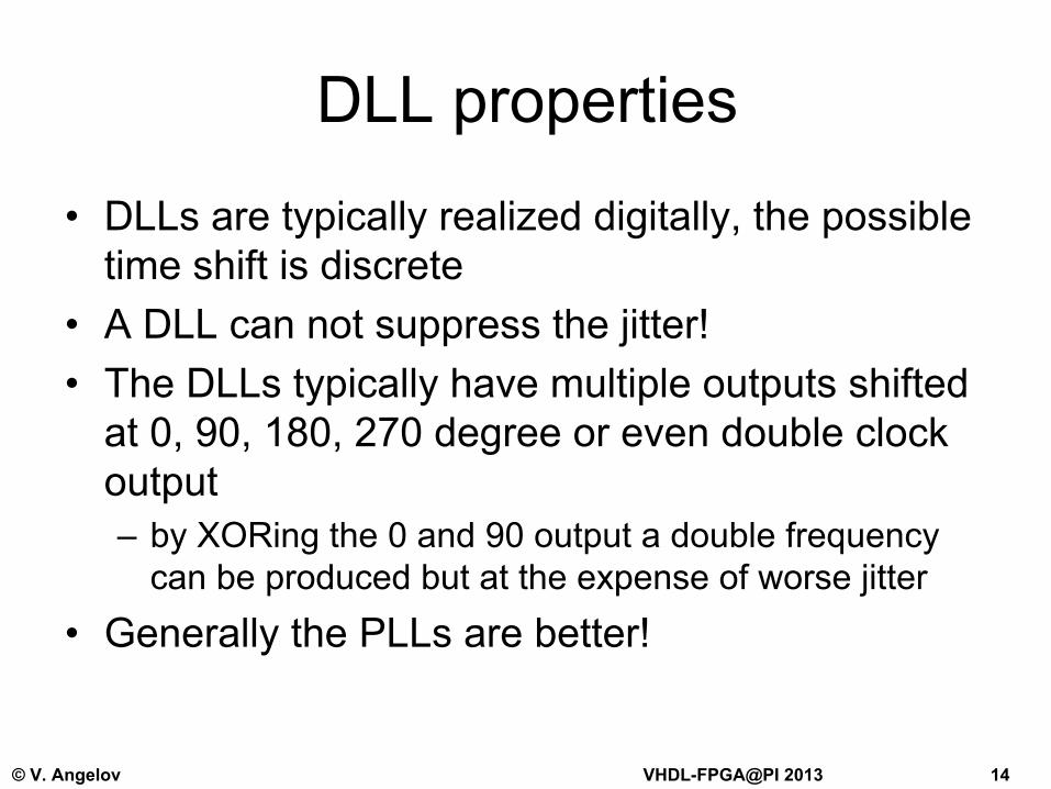
DLL properties
•
DLLs are typically realized digitally, the possible time shift is discrete
•
A DLL can not suppress the jitter!•
The DLLs typically have multiple outputs shifted at 0, 90, 180, 270 degree or even double clock output–
by XORing
the 0 and 90 output a double frequency
can be produced but at the expense of worse jitter•
Generally the PLLs
are better!
© V. Angelov VHDL-FPGA@PI 2013 15
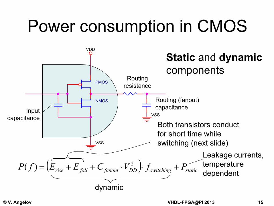
Routing (fanout) capacitance
Power consumption in CMOSVDD
VSS
PMOS
VSS
NMOS
Routing resistance
Input capacitance
( ) staticswitchingDDfanoutfallrise PfVCEEfP +⋅⋅++= 2)(
dynamic
Both transistors conduct for short time while switching (next slide)
Leakage currents, temperature dependent
Static
and dynamic components

© V. Angelov VHDL-FPGA@PI 2013 16
0
1
2
3
4
5
100 200 300 400 500 600 700
Vin,
Vou
t [V]
time [ns]
0
100
200
300
400
I [uA
]Power consumption in a CMOS
inverter
Vin
VSS
PMOS
NMOS
VDD
( )∫ ⋅= dttIVEE DDrisefall ,
Vout
© V. Angelov VHDL-FPGA@PI 2013 17
0.0
0.1
0.2
0.3
0.4
0.5
dela
y, n
s
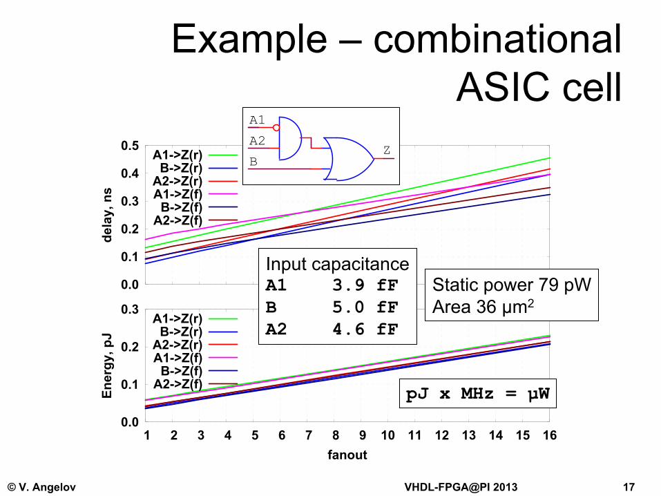
A1->Z(r)B->Z(r)
A2->Z(r)A1->Z(f)
B->Z(f)A2->Z(f)
0.0
0.1
0.2
0.3
1 2 3 4 5 6 7 8 9 10 11 12 13 14 15 16
Ener
gy, p
J
fanout
A1->Z(r)B->Z(r)
A2->Z(r)A1->Z(f)
B->Z(f)A2->Z(f)
Example – combinational ASIC cell
Input capacitanceA1
3.9 fF
B 5.0 fF
A2
4.6 fF
A1
ZB
A2
Static power 79 pWArea 36 μm2
pJ
x MHz = µW
© V. Angelov VHDL-FPGA@PI 2013 18
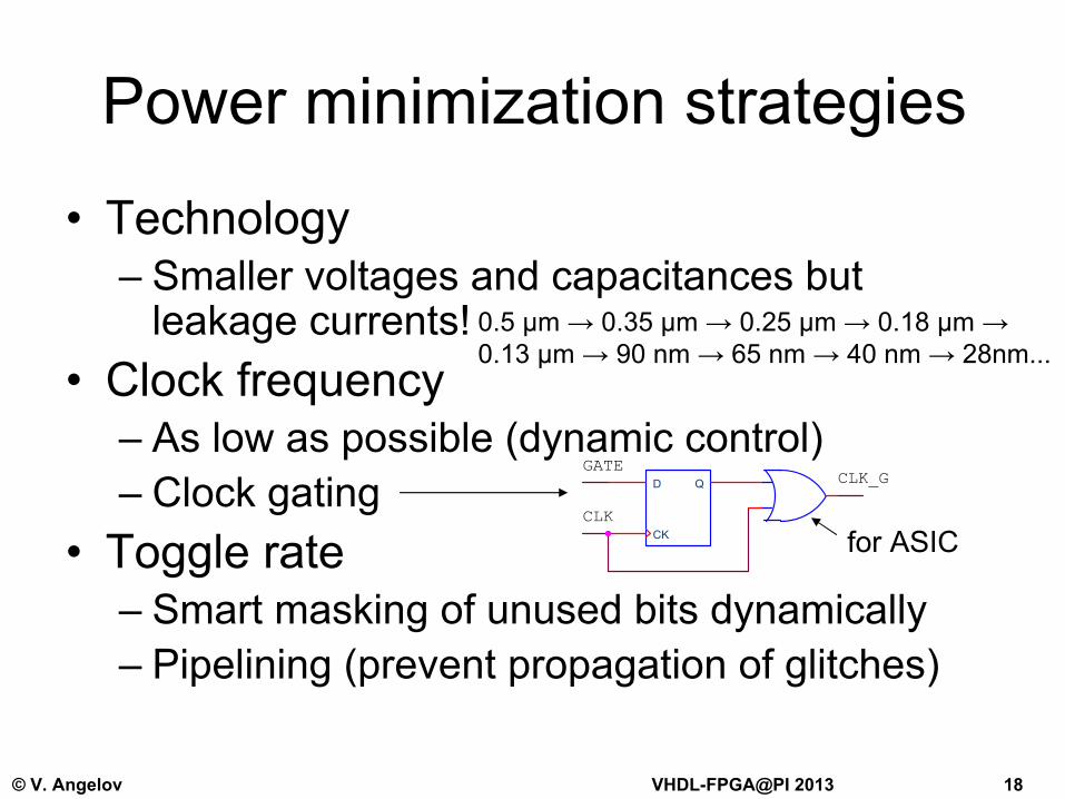
Power minimization strategies
•
Technology–
Smaller voltages and capacitances but leakage currents!
•
Clock frequency–
As low as possible (dynamic control)
–
Clock gating•
Toggle rate–
Smart masking of unused bits dynamically
–
Pipelining (prevent propagation of glitches)
D
CK
Q
CLK
CLK_GGATE
0.5 µm → 0.35 µm → 0.25 µm → 0.18 µm → 0.13 µm → 90 nm → 65 nm → 40 nm → 28nm...
for ASIC
© V. Angelov VHDL-FPGA@PI 2013 19
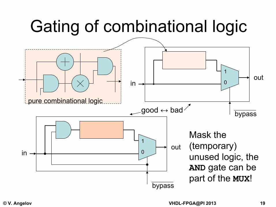
bypass
inout
pure combinational logic
Gating of combinational logic
bypass
inout
0
1
0
1
Mask the (temporary) unused logic, the AND
gate can be
part of the MUX!
good ↔ bad
© V. Angelov VHDL-FPGA@PI 2013 20
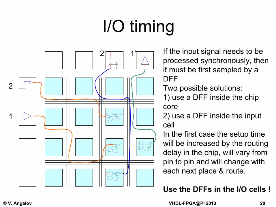
I/O timingIf the input signal needs to be processed synchronously, then it must be first sampled by a DFFTwo possible solutions:1)
use a DFF inside the chip
core2)
use a DFF inside the input
cellIn the first case the setup time will be increased by the routing delay in the chip, will vary from pin to pin and will change with each next place & route.
Use the DFFs
in the I/O cells !
2
3
5
1
D
CLK
Q
CL
D
CK
Q
2
3
5
1
D
CLK
Q
CL
1
2
2
3
5
1
D
CLK
Q
CL
D CK
Q
2
3
5
1
D
CLK
Q
CL
1’2’

© V. Angelov VHDL-FPGA@PI 2013 21
Synchronizing asynchronous signals(1)
•
Setup violations are inevitable with asynchronous
data sources
•
The DFF may oscillate if the input changes within the setup window
•
The best solution is to use two DFFs
coupled directly, without any gates in between, so the first has more time to relax
•
Use slower clocks (if possible) and faster DFFs
with min setup time to minimize the probability for oscillations
D
CK
Q D
CK
Qasync. input to the core
this is NOT a solution for synchronous inputs!
Should we use the I/O cell DFF here?
© V. Angelov VHDL-FPGA@PI 2013 22
tCO
D
CK
Q D
CK
QD1 Q2D2
CLK
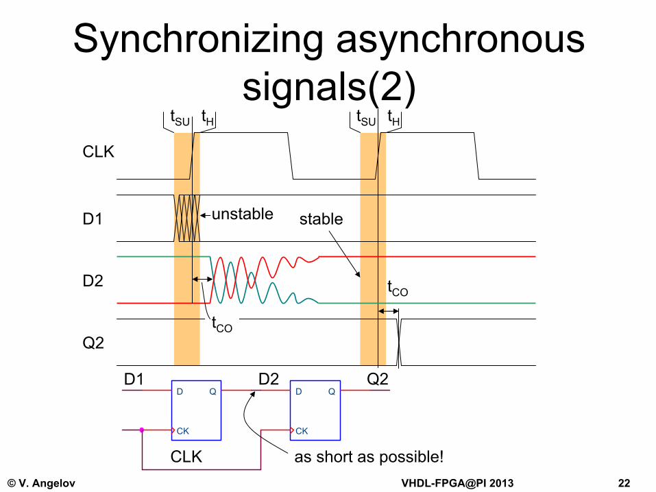
Synchronizing asynchronous signals(2)
CLK
D1
D2
Q2
stable
tSU tH
as short as possible!
unstable
tCO
tSU tH
© V. Angelov VHDL-FPGA@PI 2013 23
D
CK
QD
CK
Q
tCO
D1 Q2D2
CLK
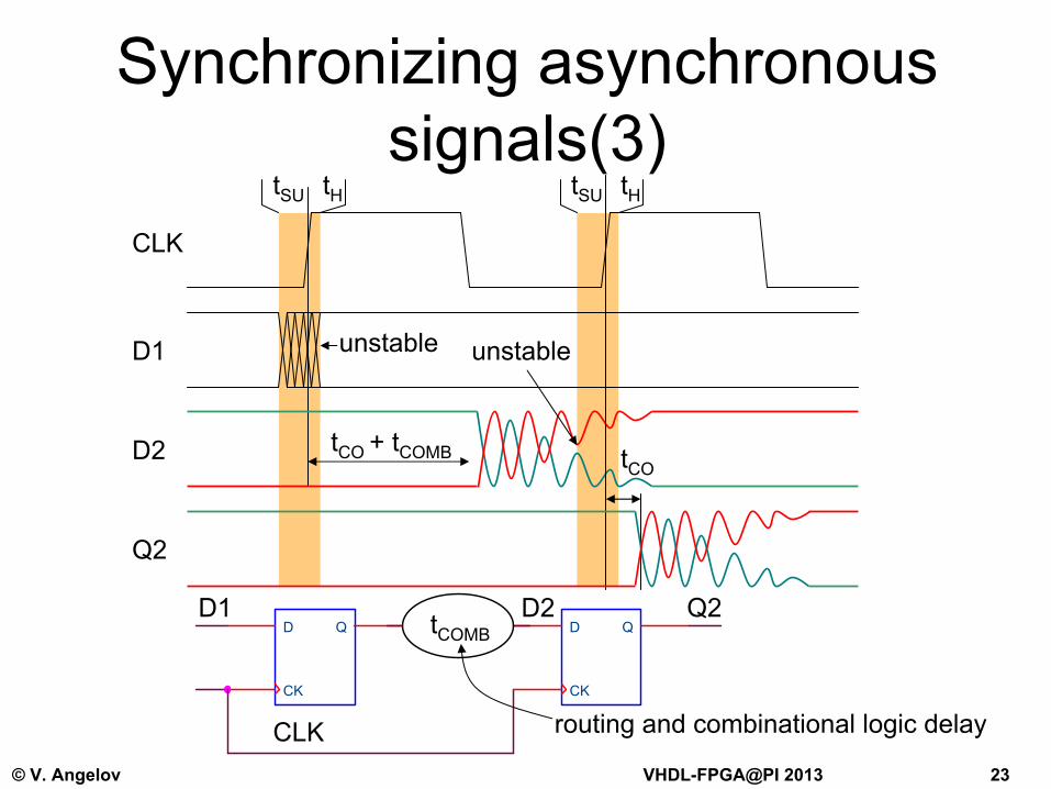
Synchronizing asynchronous signals(3)
CLK
D1
D2
Q2
unstable
tSU tH
tCO
+ tCOMB
tCOMB
unstable
routing and combinational logic delay
tSU tH
© V. Angelov VHDL-FPGA@PI 2013 24
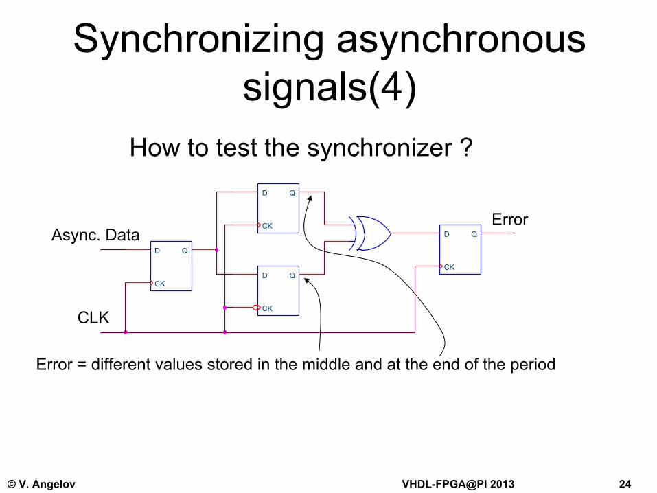
Synchronizing asynchronous signals(4)
D
CK
Q
D
CK
Q
D
CK
Q
D
CK
Q
Error
CLK
Async. Data
Error = different values stored in the middle and at the end of the period
How to test the synchronizer ?
© V. Angelov VHDL-FPGA@PI 2013 25
Input pins•
In some FPGAs
programmable input delays are
available to move the sampling window of the data relative to the clock–
Set constraints on the input setup/hold time!
•
The input cells can be programmed for various levels (5V, 3.3V, 2.5V, 1.8V, LVTTL, LVCMOS)–
read carefully the data sheets and the board documentation!
•
Programmable pull-up/down resistors are usually available –
use them for inputs which are not always
connected to prevent floating–
floating inputs increase the power consumption of the chip and introduce noise

© V. Angelov VHDL-FPGA@PI 2013 26
Output pins•
Similarly when some output signal is synchronous to the clock, use the output DFFs
in the I/O cells to have well
defined clock to output delay!•
In some FPGAs
programmable output delays are
available–
set constraints for clock to output!
•
The slew rate of the output cells is usually programmable–
try to use the slow slew rate option on most of the outputs to prevent large current spikes on the VIO
•
The output pins are limited to source/sink currents, there are maximum recommended values per pin, per I/O bank (a group of pins)–
read carefully the datasheets!
© V. Angelov VHDL-FPGA@PI 2013 27
D (PIN)
Y (PIN)A (PIN)
Q (PIN)D
CK
Q D
CK
Q
CLK (PIN)
B (PIN)
Timing parameters (summary)
tCIN
tDIN
tSU tH tCO
tCOMB_FF
tQOUT
period T
D(PIN) setup = tDIN
+ tSU
– tCIN
D(PIN) hold = tH
– (tDIN
– tCIN
)TMIN
= tCO
+ tCOMB_FF
+ tSU
Q(PIN) clock to output = tCIN
+ tCO
+ tQOUT
tCOMB
tPD
(A→Y)=tA
+ tCOMB
+ tYOUT
tA
tB
tYOUT
© V. Angelov VHDL-FPGA@PI 2013 28
Gate level and timing simulations
•
The simulations in the FPGA design flow•
Why do we need different types of simulations?
•
ModelSim
simulations of Xilinx and Altera FPGAs
–
gate level, timing (with backannotation)–
directory structure, Makefile

© V. Angelov VHDL-FPGA@PI 2013 29
Design flow CPLD/FPGA
Your favourite text editor!Some recommendations: emacs, notepad++, nedit, with syntax colouring and more for VHDL
and Verilog
LeoSpecPrecisionSynplify
FPGA vendorsSynopsys
ModelSimAldec
AHDL
FPGA vendor
Device programming
Each step can take seconds, minutes, hours ... (place & route)
functional simulation
synthesis
timing estimation
gate-level simulation
place & route
sdf
simulation
timing analysis
design entry: schematic, HDL
board production
& test
© V. Angelov VHDL-FPGA@PI 2013 30
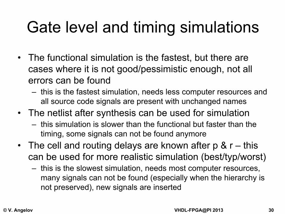
Gate level and timing simulations
•
The functional simulation is the fastest, but there are cases where it is not good/pessimistic enough, not all errors can be found–
this is the fastest simulation, needs less computer resources and all source code signals are present with unchanged names
•
The netlist
after synthesis can be used for simulation–
this simulation is slower than the functional but faster than the timing, some signals can not be found anymore
•
The cell and routing delays are known after p & r –
this can be used for more realistic simulation (best/typ/worst)–
this is the slowest simulation, needs most computer resources, many signals can not be found (especially when the hierarchy is not preserved), new signals are inserted
© V. Angelov VHDL-FPGA@PI 2013 31
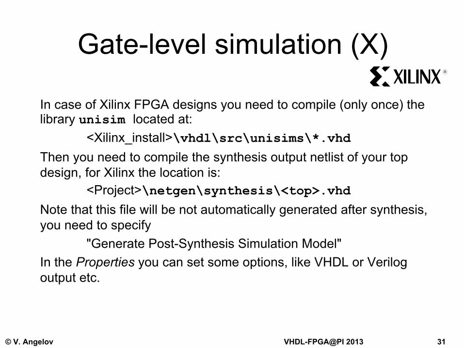
Gate-level simulation (X)
In case of Xilinx FPGA designs you need to compile (only once) the library unisim
located at:
<Xilinx_install>\vhdl\src\unisims\*.vhdThen you need to compile the synthesis output netlist
of your top
design, for Xilinx the location is:<Project>\netgen\synthesis\<top>.vhd
Note that this file will be not automatically generated after synthesis, you need to specify
"Generate Post-Synthesis Simulation Model"In the Properties
you can set some options, like VHDL or Verilog
output etc.
R

© V. Angelov VHDL-FPGA@PI 2013 32
Timing Simulation (X)Typically done after placing and routing of the design.In case of Xilinx FPGA designs you need to compile (only once) the library simprim
located at:
<Xilinx_install>\vhdl\src\simprims\*_mti.vhdThen you need to compile the output netlist, for Xilinx the location is:
<Project>\netgen\par\<top>.vhdThe simulation tool needs the timing information, stored in the Standard Delay File (SDF):
<Project>\netgen\par\<top>.sdfNote that these files will be not automatically generated after P & R, you need to specify
"Generate Post-Place & Route Simulation Model"In the Properties
you can set some options, like VHDL or Verilog
output etc.
R
© V. Angelov VHDL-FPGA@PI 2013 33
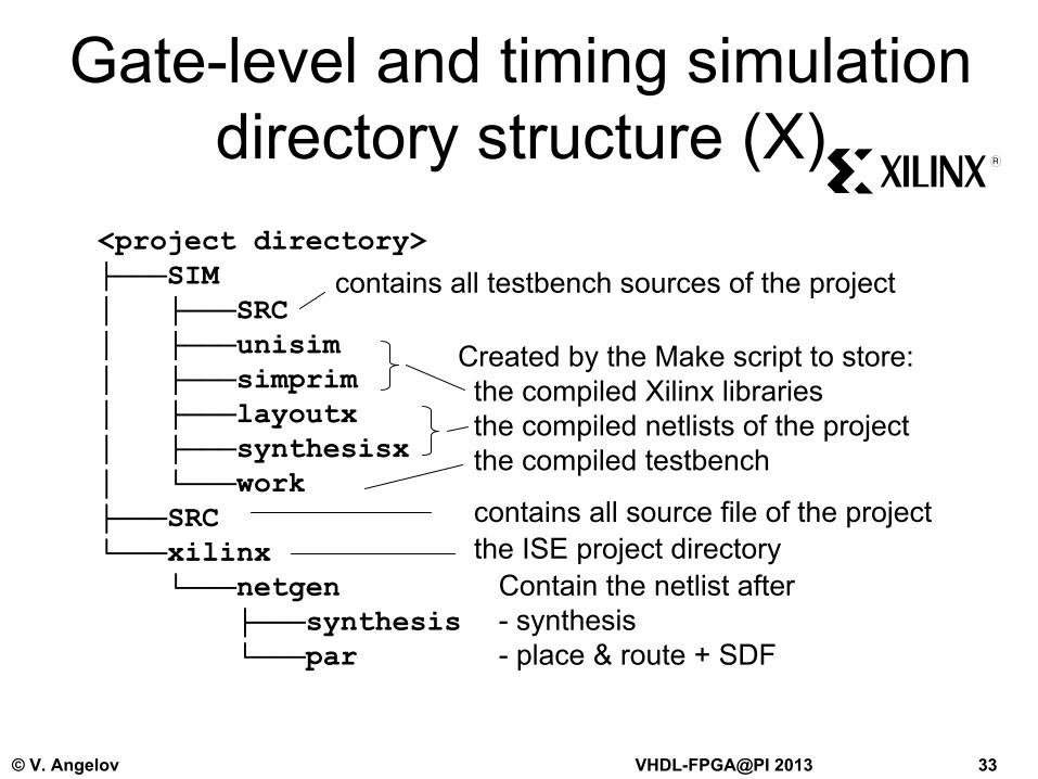
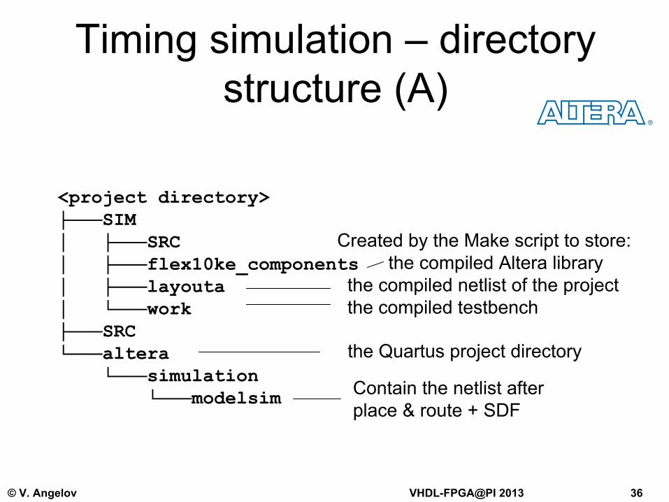
Gate-level and timing simulation directory structure (X)
R
<project directory>├───SIM│
├───SRC
│
├───unisim│
├───simprim
│
├───layoutx│
├───synthesisx
│
└───work├───SRC└───xilinx
└───netgen├───synthesis└───par
Created by the Make script to store:the compiled Xilinx librariesthe compiled netlists
of the project
the compiled testbench
contains all testbench
sources of the project
Contain the netlist
after- synthesis-
place & route + SDF
contains all source file of the projectthe ISE project directory
© V. Angelov VHDL-FPGA@PI 2013 34
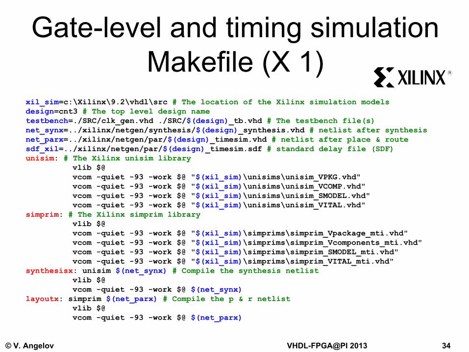
Gate-level and timing simulation Makefile (X 1)
xil_sim=c:\Xilinx\9.2\vhdl\src # The location of the Xilinx simulation modelsdesign=cnt3 # The top level design nametestbench=./SRC/clk_gen.vhd ./SRC/$(design)_tb.vhd # The testbench file(s)net_synx=../xilinx/netgen/synthesis/$(design)_synthesis.vhd # netlist after synthesisnet_parx=../xilinx/netgen/par/$(design)_timesim.vhd # netlist after place & routesdf_xil=../xilinx/netgen/par/$(design)_timesim.sdf # standard
delay
file
(SDF)unisim: # The Xilinx unisim library
vlib $@vcom -quiet -93 -work $@ "$(xil_sim)\unisims\unisim_VPKG.vhd"vcom -quiet -93 -work $@ "$(xil_sim)\unisims\unisim_VCOMP.vhd"vcom -quiet -93 -work $@ "$(xil_sim)\unisims\unisim_SMODEL.vhd"vcom -quiet -93 -work $@ "$(xil_sim)\unisims\unisim_VITAL.vhd"
simprim: # The Xilinx simprim libraryvlib $@vcom -quiet -93 -work $@ "$(xil_sim)\simprims\simprim_Vpackage_mti.vhd"vcom -quiet -93 -work $@ "$(xil_sim)\simprims\simprim_Vcomponents_mti.vhd"vcom -quiet -93 -work $@ "$(xil_sim)\simprims\simprim_SMODEL_mti.vhd"vcom -quiet -93 -work $@ "$(xil_sim)\simprims\simprim_VITAL_mti.vhd"
synthesisx: unisim $(net_synx) # Compile the synthesis netlistvlib $@vcom -quiet -93 -work $@ $(net_synx)
layoutx: simprim $(net_parx) # Compile the p & r netlistvlib $@vcom -quiet -93 -work $@ $(net_parx)
R
© V. Angelov VHDL-FPGA@PI 2013 35
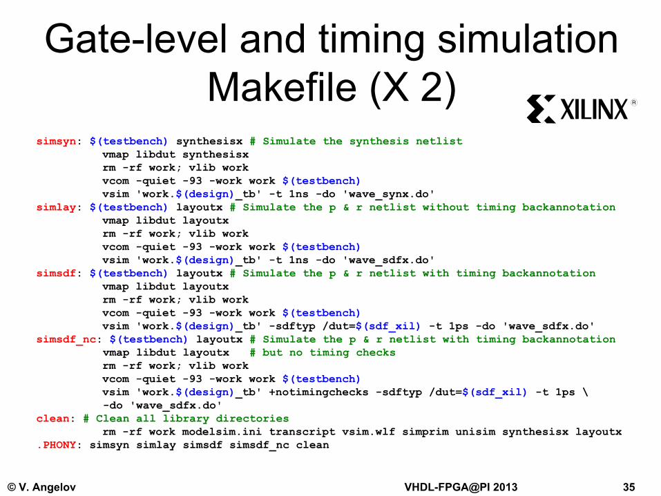
Gate-level and timing simulation Makefile (X 2)simsyn: $(testbench)
synthesisx # Simulate the synthesis netlistvmap libdut synthesisxrm -rf work; vlib workvcom -quiet -93 -work work $(testbench)vsim 'work.$(design)_tb' -t 1ns -do 'wave_synx.do'
simlay: $(testbench)
layoutx # Simulate the p & r netlist without timing backannotationvmap libdut layoutxrm -rf work; vlib workvcom -quiet -93 -work work $(testbench)vsim 'work.$(design)_tb' -t 1ns -do 'wave_sdfx.do'
simsdf: $(testbench)
layoutx # Simulate the p & r netlist with timing backannotationvmap libdut layoutxrm -rf work; vlib workvcom -quiet -93 -work work $(testbench)vsim 'work.$(design)_tb' -sdftyp /dut=$(sdf_xil)
-t 1ps -do 'wave_sdfx.do'simsdf_nc: $(testbench)
layoutx # Simulate the p & r netlist with timing backannotationvmap libdut layoutx # but no timing checksrm -rf work; vlib workvcom -quiet -93 -work work $(testbench)vsim 'work.$(design)_tb' +notimingchecks -sdftyp /dut=$(sdf_xil)
-t 1ps \-do 'wave_sdfx.do'
clean: # Clean all library directoriesrm -rf work modelsim.ini transcript vsim.wlf simprim unisim synthesisx layoutx
.PHONY: simsyn simlay simsdf simsdf_nc clean
R
© V. Angelov VHDL-FPGA@PI 2013 36
Timing simulation – directory structure (A)
Created by the Make script to store:the compiled Altera
library
the compiled netlist
of the projectthe compiled testbench
<project directory>├───SIM│
├───SRC
│
├───flex10ke_components│
├───layouta
│
└───work├───SRC└───altera
└───simulation└───modelsim Contain the netlist
after
place & route + SDF
the Quartus
project directory

© V. Angelov VHDL-FPGA@PI 2013 37
Timing simulation Makefile (A)alt_sim=d:\Programme\q81\quartus\eda\sim_lib # The location of the Altera sim. modelsalt_family=flex10ke # Note that the family depends on the chip used in the project!alt_lib=$(alt_family)_componentsdesign=cnt3 # The top level design nametestbench=./SRC/clk_gen.vhd ./SRC/$(design)_tb.vhd # The testbench file(s) net_para=../altera/simulation/modelsim/$(design).vho # netlist after place & routesdf_alt=../altera/simulation/modelsim/$(design)_vhd.sdo # standard delay file (SDF)$(alt_lib):
vlib $@vcom -quiet -93 -work $@ "$(alt_sim)\$(alt_family)_atoms.vhd"vcom -quiet -93 -work $@ "$(alt_sim)\$(alt_family)_components.vhd"vmap $(alt_family)
$@layouta: $(alt_lib)
$(net_para)vlib $@; vcom -quiet -93 -work $@ $(net_para)
simlay: $(testbench)
layouta # Simulate the p & r netlist withoutvmap libdut layouta # timing backannotationrm -rf work; vlib workvcom -quiet -93 -work work $(testbench)vsim 'work.$(design)_tb' -t 1ns -do 'wave_sdfa.do'
simsdf: $(testbench)
layouta # Simulate the p & r netlist withvmap libdut layouta # timing backannotationrm -rf work; vlib workvcom -quiet -93 -work work $(testbench)vsim 'work.$(design)_tb' -sdftyp /dut=$(sdf_alt)
-t 1ps -do 'wave_sdfa.do'clean: # Clean all library directories
rm -rf functional work modelsim.ini transcript vsim.wlf $(alt_lib)
layouta.PHONY: simlay simsdf clean
© V. Angelov VHDL-FPGA@PI 2013 38
Recommendations (1)•
Do not use the text editors of the FPGA vendor software tools and of the simulation tools! These programs are not very stable, you can easily lose your work!
•
Portability for code reuse:–
Do not use the FPGA vendor software tools for simulations, and if possible avoid synthesis with them to have more independent design flow
–
Avoid using specific FPGA library components•
Do not work only with GUI –
try to find out how the software stores all important parameters
in the
corresponding text files and edit them directly (e.g. constraint
files)–
If possible write scripts for all steps (make), many programs create them automatically –
so you can be sure that all steps are done in the right
order next time, doing this by mouse clicking is not very reliable

© V. Angelov VHDL-FPGA@PI 2013 39
Recommendations (2)•
Avoid becoming a fanatic fan of some FPGA vendor –
for each application take the best suitable chip, if your HDL code follows the recommendations above, it will be portable and easy to change the technology
•
Maintain your HDL code in repositories (CVS, SVN). Some FPGA software tools offer version control –
nobody knows how it works, in most cases not as expected, do not rely on it!
•
Put your sources in a well organized directory tree, DO NOT MIX with the hundreds of files generated by the software!