the new low noise control system for the virgo suspensions alberto gennai the virgo collaboration
TRANSCRIPT

The New Low Noise Control System The New Low Noise Control System For The VIRGO SuspensionsFor The VIRGO Suspensions
Alberto Gennai
The VIRGO Collaboration
Australia-Italy Workshop October 4-7 2005
A.Gennai (INFN Pisa) 2
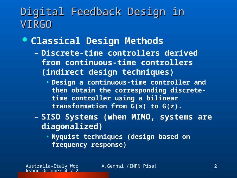
Digital Feedback Design in VIRGODigital Feedback Design in VIRGO
Classical Design Methods– Discrete-time controllers derived from
continuous-time controllers (indirect design techniques)
• Design a continuous-time controller and then obtain the corresponding discrete-time controller using a bilinear transformation from G(s) to G(z).
– SISO Systems (when MIMO, systems are diagonalized)
• Nyquist techniques (design based on frequency response)
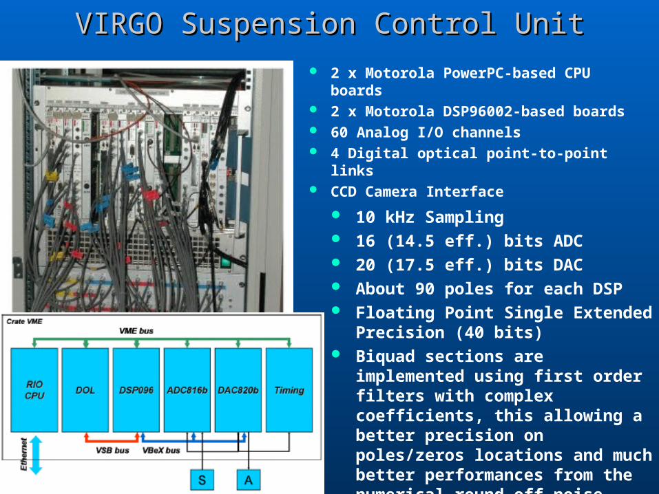
VIRGO Suspension Control UnitVIRGO Suspension Control Unit
2 x Motorola PowerPC-based CPU boards
2 x Motorola DSP96002-based boards 60 Analog I/O channels 4 Digital optical point-to-point links CCD Camera Interface
10 kHz Sampling 16 (14.5 eff.) bits ADC 20 (17.5 eff.) bits DAC About 90 poles for each DSP Floating Point Single Extended
Precision (40 bits) Biquad sections are implemented
using first order filters with complex coefficients, this allowing a better precision on poles/zeros locations and much better performances from the numerical round-off noise.

Australia-Italy Workshop October 4-7 2005
A.Gennai (INFN Pisa) 4
VIRGO DSP Application Process ViewVIRGO DSP Application Process View
Analog I/O
DSP OS
DSP ISR
Trigger
EServerDSP
DAQ
GlobalControl
User Interface VMECm
User
DSPrioAWS
Analog I/O
Analog I/O
DSP OSDSP OS
DSP ISRDSP ISR
Trigger
EServerDSPEServerDSP
DAQDAQ
GlobalControlGlobalControl
User InterfaceUser Interface VMECm
UserUser
DSPrioAWS
Australia-Italy Workshop October 4-7 2005
A.Gennai (INFN Pisa) 5
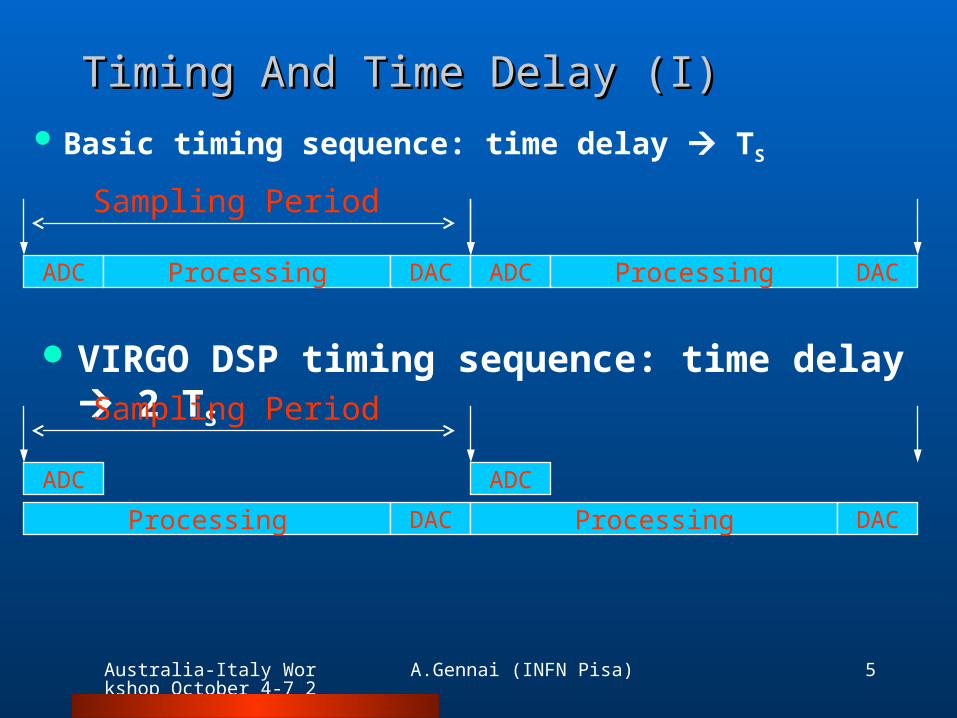
Timing And Time Delay (I)Timing And Time Delay (I)
Basic timing sequence: time delay TS
ADC Processing DAC ADC Processing DAC
Sampling Period
VIRGO DSP timing sequence: time delay 2 TS
ADC
Processing DAC
Sampling Period
ADC
Processing DAC

Australia-Italy Workshop October 4-7 2005
A.Gennai (INFN Pisa) 6
Timing And Time Delay (II)Timing And Time Delay (II)
Total Delay Contributions– Sampling Period
• ADC and DAC conversion time• Processing Time• ISR latency and context switch time
– DAC Hold Time = 0.5 TS
– Anti-Aliasing and Reconstruction Filters
Total Delay (Local Control)T = 2 Ts + 0.5 TS + 4 TS = 6.5 Ts (TS = 100 sec)
For Global Control we need one additional TS for GC processing

Australia-Italy Workshop October 4-7 2005
A.Gennai (INFN Pisa) 7
VIRGO DSPVIRGO DSP About 80 usecs available for computation 8 poles + 8 zeros = 1 usec Current limits
– Total number of variables + total number of filters coefficients cannot exceed 512 (128 var + 384 coeff). In terms of number of singularities we have a maximum of 128 poles + 128 zeros that can be extended up to 192 poles and 192 zeros allowing some additional computation time.
• This limit was reached and big efforts are now needed in code optimization
– Computation Time: close to limit for DSP controlling suspension top stage.
– I/O: Limited number of I/O channels (40) • Limit reached and influencing some architectural choice.
DSP processor obsolete

Australia-Italy Workshop October 4-7 2005
A.Gennai (INFN Pisa) 8
DSP Code Example: MC Local ControlDSP Code Example: MC Local Control
On top of already quite complex algorithms, new functionalities were added:– Mirror position
memory– Automatic re-lock
Australia-Italy Workshop October 4-7 2005
A.Gennai (INFN Pisa) 9
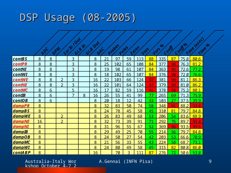
DSP Usage (08-2005)DSP Usage (08-2005)
ADCDPM
Ser In
/ Out
GLB In
GLB Out
DACPro
bes
Poles
Zeros
Vars
Vars
%
Coeff
Coeff %
Time
(use
c)
Time
%
contBS 8 8 3 8 21 97 59 113 88 335 87 75.8 80.6contPR 8 8 3 8 25 102 65 108 84 377 98 76.3 81.2contNI 8 8 3 8 19 98 61 107 84 363 95 72.6 77.2contWI 8 8 3 8 18 102 65 107 84 376 98 72.0 76.6contWE 8 8 2 3 16 22 103 66 124 97 381 99 81.1 86.3contNE 8 8 2 3 16 22 101 64 124 97 379 99 81.0 86.2contMC 8 6 5 16 17 82 59 116 91 378 98 75.3 80.1contIB 8 6 7 8 16 26 55 41 99 77 265 69 71.3 75.9contOB 8 6 8 20 18 12 42 33 103 27 37.5 39.9dampPR 8 8 32 83 50 74 58 348 91 88.2 93.8dampBS 8 8 24 78 45 58 45 310 81 79.7 84.8dampWE 8 2 8 26 83 49 68 53 206 54 83.6 88.9dampNE 16 2 8 32 73 39 91 71 292 76 89.7 95.4dampNI 8 8 31 96 55 67 52 369 96 93.5 99.5dampIB 8 8 29 49 25 70 55 214 56 79.7 84.8dampOB 8 8 24 50 27 54 42 203 53 66.6 70.9dampMC 8 8 21 56 33 55 43 224 58 68.7 73.1dampWI 8 8 24 80 49 58 45 315 82 80.8 86.0contABP 8 16 70 3 111 87 276 72 50.6 53.8
Australia-Italy Workshop October 4-7 2005
A.Gennai (INFN Pisa) 10
New Control SystemNew Control System Scope
– Upgrade of the main control loops of Virgo (suspensions, injection, locking and alignment) aiming to faster and higher dynamical range control systems.
Motivations– The control system currently in use is operative since
1998 (project started in 1994) and it is now approaching its limits in terms of performances for available computational power, converters dynamical range and components availability.
– The new control system foresees multi-DSP computing units, faster and higher resolution analog-to-digital and digital-to-analog converters and high dynamic power driver for coil-magnet pair actuators.
Australia-Italy Workshop October 4-7 2005
A.Gennai (INFN Pisa) 11
Running activities and development planRunning activities and development plan New Signal Processing Board
– Design completed in October 2004 – First prototype currently under test (September 2005)
New Coil-Driver– Prototypes currently installed at VIRGO terminal towers
and beam splitter tower.– Final design completed January 2005– First production and installation in 2006
New Digital to Analog Converter Board– Early design phase
Software Development– Preliminary design phase for both DSP compiler and top
level control software

Australia-Italy Workshop October 4-7 2005
A.Gennai (INFN Pisa) 12
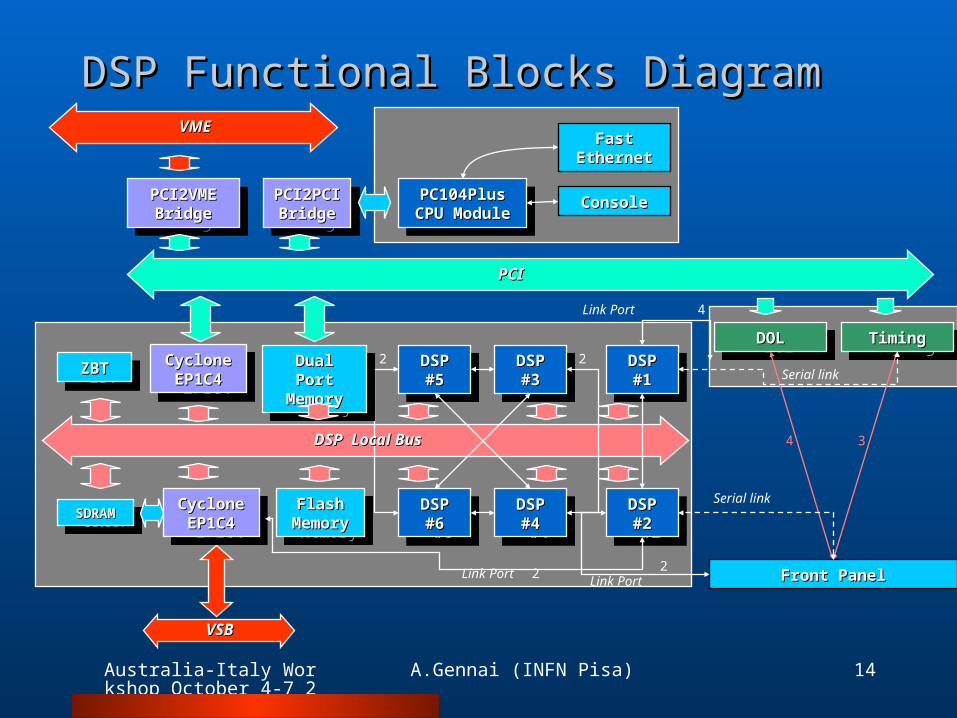
Multiprocessor DSP Board: Main FeaturesMultiprocessor DSP Board: Main Features 6 x 100 MHz ADSP211160N SHARC DSP 3.4 GigaFLOPS in single PMC Mezzanine 1800 MB/s of low latency inter processor communication bandwidth 512 MB SDRAM, 4 MB ZBT SRAM, 4Mbit FLASH EPROM 64-bit 66 MHz PCI bus ready Up to 2 x PC/104-Plus Intel Celeron 933 MHz modules with Fast Ethernet
interface running Linux OS 1 PMC Mezzanine site for optional PowerPC or Pentium based CPU 1 PMC Mezzanine site for digital optical link and timing interface On board 32-bit Master-Slave PCI to DSP Local Bus bridge 256 kWord real Dual Port memory (PCI – DSP LB) VME to PCI Master – Slave bridge DSP LB to VSB bridge for I/O devices access 200 MB/s auxiliary I/O bandwidth IEEE 1149.1 JTAG Standard Test Access Port 2 x Altera EP1C4 Cyclone FPGA Advanced software support from Altera Quartus II suite VisualDSP++ support Virgo DSP compiler

Australia-Italy Workshop October 4-7 2005
A.Gennai (INFN Pisa) 13
Why 3 GFLOPS ?Why 3 GFLOPS ?
Additional computational power will allow implementing MIMO and adaptive controllers, with major advantages from the so called “control noise” point of view
Present DSPs are overloaded by data reduction and processing activities that cannot be handled by the central VIRGO data acquisition system. Multiple DSPs will allow keeping on implementing such functionalities without loading nodes devote to control tasks.
Australia-Italy Workshop October 4-7 2005
A.Gennai (INFN Pisa) 14
VSBVSB
VMEVME
PCIPCI
PCI2VMEPCI2VMEBridgeBridge
PCI2VMEPCI2VMEBridgeBridge
PCI2PCIPCI2PCIBridgeBridge
PCI2PCIPCI2PCIBridgeBridge
PC104PlusPC104PlusCPU ModuleCPU Module
PC104PlusPC104PlusCPU ModuleCPU Module
FastFastEthernetEthernet
ConsoleConsole
DOLDOLDOLDOL TimingTimingTimingTiming
Front PanelFront Panel
Serial link
Serial link
4 3
DSPDSP#5#5
DSPDSP#5#5
DSPDSP#6#6
DSPDSP#6#6
DSPDSP#3#3
DSPDSP#3#3
DSPDSP#4#4
DSPDSP#4#4
DSPDSP#1#1
DSPDSP#1#1
DSPDSP#2#2
DSPDSP#2#2
FlashFlashMemoryMemory
FlashFlashMemoryMemory
Dual Port Dual Port MemoryMemory
Dual Port Dual Port MemoryMemory
2
2 2
2Link Port
Link Port
DSP Local BusDSP Local Bus
CycloneCycloneEP1C4EP1C4
CycloneCycloneEP1C4EP1C4
SDRAMSDRAMSDRAMSDRAM CycloneCyclone
EP1C4EP1C4
CycloneCycloneEP1C4EP1C4
ZBTZBTZBTZBT
4Link Port
DSP Functional Blocks DiagramDSP Functional Blocks Diagram

Australia-Italy Workshop October 4-7 2005
A.Gennai (INFN Pisa) 15
DSP Board DescriptionDSP Board Description
ADSP 21160N DSPLike other SHARCs, the ADSP-21160N is a 32-bit processor that is optimized for high performance DSP applications.
The ADSP-21160N features include an 95 MHz core, a 4M-bit dual-ported on-chip SRAM, an integrated I/O processor that supports 14 DMA channels, multiple internal buses to eliminate I/O bottlenecks, two serial ports, six link ports, external parallel bus, and glueless multiprocessing.
The ADSP-21160N introduces Single-Instruction, Multiple-Data (SIMD) processing. Using two computational units (ADSP-2106x SHARC DSPs have one), the ADSP-21160N can double performance versus the ADSP-2106x on a range of DSP algorithms.
With its SIMD computational hardware running at 95 MHz, the ADSP-21160N can perform 570 million math operations per second.
Australia-Italy Workshop October 4-7 2005
A.Gennai (INFN Pisa) 16
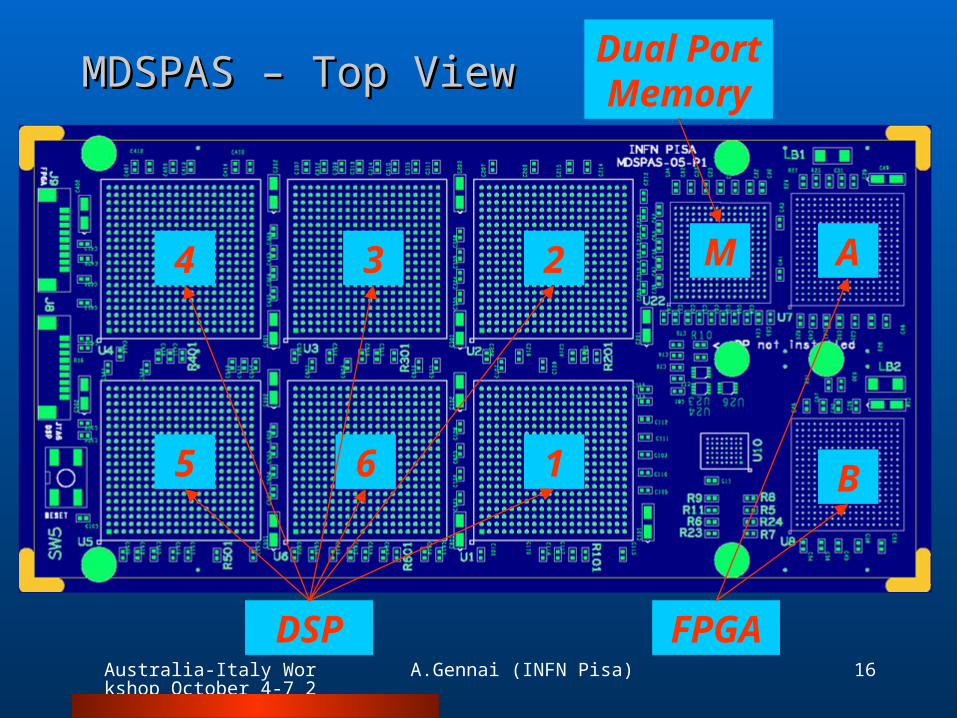
MDSPAS – Top ViewMDSPAS – Top View
DSP
1
234
5 6
AM
FPGA
B
Dual Port Memory

Australia-Italy Workshop October 4-7 2005
A.Gennai (INFN Pisa) 17
MDSPAS – Bottom ViewMDSPAS – Bottom View
SDRAM
PCI 64 – 66 MHz
VSBbusI/O TimDOL
Australia-Italy Workshop October 4-7 2005
A.Gennai (INFN Pisa) 18
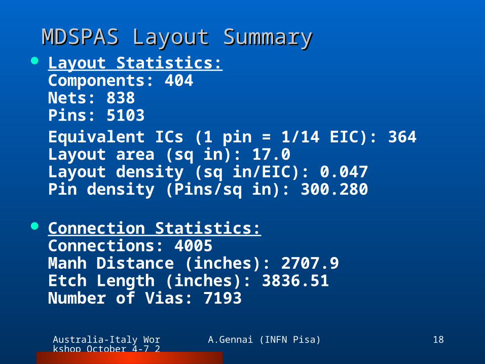
MDSPAS Layout SummaryMDSPAS Layout Summary Layout Statistics:
Components: 404Nets: 838Pins: 5103
Equivalent ICs (1 pin = 1/14 EIC): 364Layout area (sq in): 17.0Layout density (sq in/EIC): 0.047Pin density (Pins/sq in): 300.280
Connection Statistics:Connections: 4005Manh Distance (inches): 2707.9Etch Length (inches): 3836.51Number of Vias: 7193

DSP Board: First prototype under testDSP Board: First prototype under test

Australia-Italy Workshop October 4-7 2005
A.Gennai (INFN Pisa) 20
MDSPAS – Lay up and viasMDSPAS – Lay up and vias
Nr Name Type Material Thickness (um) VIA2T VIA4T VIA6T VIA6B VIA4B VIA2B VIAP VIAPP1 TOP CONDUCTOR COPPER 35 Via Pad Size (um) 400 400 400 450 710
DIELECTRIC FR-4 1502 L2 CONDUCTOR COPPER 35 400 400 400 450 710
DIELECTRIC FR-4 1503 GNDT PLANE COPPER 35 400 400 450 710
DIELECTRIC FR-4 1504 L4 CONDUCTOR COPPER 35 400 400 450 710
DIELECTRIC FR-4 1505 VDDI PLANE COPPER 35 400 450 710
DIELECTRIC FR-4 1506 VCORE PLANE COPPER 35 400 450 710
DIELECTRIC FR-4 1507 L7 CONDUCTOR COPPER 35 400 450 710
DIELECTRIC FR-4 1508 VDDE PLANE COPPER 35 400 450 710
DIELECTRIC FR-4 1509 L9 CONDUCTOR COPPER 35 400 400 450 710
DIELECTRIC FR-4 15010 GNDB PLANE COPPER 35 400 400 450 710
DIELECTRIC FR-4 15011 L11 CONDUCTOR COPPER 35 400 400 400 450 710
DIELECTRIC FR-4 15012 BOTTOM CONDUCTOR COPPER 35 400 400 400 450 710
Drill Size (um) 200 200 200 200 200 200 250 400

Australia-Italy Workshop October 4-7 2005
A.Gennai (INFN Pisa) 21VME Connectors
DSP
Motherboard TopMotherboard Top
DOL& Timing
Australia-Italy Workshop October 4-7 2005
A.Gennai (INFN Pisa) 22
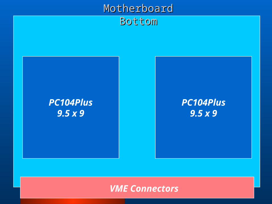
PC104Plus9.5 x 9
PC104Plus9.5 x 9
VME Connectors
Motherboard BottomMotherboard Bottom

Australia-Italy Workshop October 4-7 2005
A.Gennai (INFN Pisa) 23
New Coil DriversNew Coil Drivers Power amplifiers used to drive coil-magnet pair actuators
steering VIRGO optical elements need a dynamical range wider than what initially foreseen due to the big force impulse required to acquire the lock of VIRGO optical cavities.
A new coil driver was designed using two distinct sections: one high power section for lock acquisition and one low noise section for linear regime. The two sections are driven by two independent digital to analog converter channels. The new coil driver can supply up to 3 A during the lock acquisition phase with a few nA/Hz1/2 of noise during linear regime.
A final version of the new coil driver will host three distinct sections and the possibility to add digital to analog converters on board to improve EMI/EMC

Australia-Italy Workshop October 4-7 2005
A.Gennai (INFN Pisa) 24
Actuator noise: current status
Overview and MotivationsOverview and Motivations
10-1
100
101
102
103
10-20
10-15
10-10
10-5
Actuators noise: current status
Frequency (Hz)
m/H
z1/2
Reference Mass - Mirror Actuators NoiseFilter #7 - Marionetta Actuators NoiseVIRGO Sentivity
Initial VIRGO setup
Australia-Italy Workshop October 4-7 2005
A.Gennai (INFN Pisa) 25
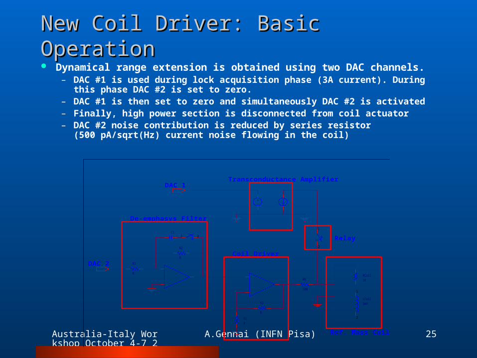
New Coil Driver: Basic OperationNew Coil Driver: Basic Operation
LCoil3mH
1
2
RCoil10
Ref. Mass Coil
+
-
OUT
R2
R
R1R
Coil Driver
DAC 2
RN
500
DAC 1Transconductance Amplifier
1
2
Relay
+
-
OUT
R1
R
R2
R
C11 2
De-emphasys Filter
Dynamical range extension is obtained using two DAC channels.– DAC #1 is used during lock acquisition phase (3A current). During
this phase DAC #2 is set to zero.– DAC #1 is then set to zero and simultaneously DAC #2 is activated– Finally, high power section is disconnected from coil actuator– DAC #2 noise contribution is reduced by series resistor
(500 pA/sqrt(Hz) current noise flowing in the coil)

Australia-Italy Workshop October 4-7 2005
A.Gennai (INFN Pisa) 26
Preliminary Desing (Protoype)Preliminary Desing (Protoype)
A prototype was developed modifying existing coil drivers to test theory of operation
Control functionalities were implemented using external devices

Australia-Italy Workshop October 4-7 2005
A.Gennai (INFN Pisa) 27
0 10 20 30 40 50 60-8
-6
-4
-2
0
2
4
6
8
Time (s ec)
Cur
rent
Mon
itor
Coil UpCoil DownSwitch
Time
0 10 20 30 40 50 60-8
-6
-4
-2
0
2
4
6
8
Time (s ec)
Cur
rent
Mon
itor
Coil UpCoil DownSwitch
Time
Preliminary Desing (cont.)Preliminary Desing (cont.)
No problems were noticed during prototype operation (now installed at terminal and beam spltter mirrors) excluding ...
100
101
102
103
104
10-6
10-5
10-4
10-3
10-2
10-1
100
Frequency (Hz)
PSD
(V
/sqr
t(H
z))
High Power GPS 778606100Low Noise GPS 778606730High Power GPS 778606970Low Noise GPS 778607600
200 A/V
Current monitoring noise
DAC noise floor
DAC noise floor with new coil driver
100
101
102
103
104
10-6
10-5
100
101
102
103
104
10-6
10-5
10-4
10-3
10-2
10-1
100
10-4
10-3
10-2
10-1
100
Frequency (Hz)
PSD
(V
/sqr
t(H
z))
High Power GPS 778606100Low Noise GPS 778606730High Power GPS 778606970Low Noise GPS 778607600
200 A/V
Current monitoring noise
DAC noise floor
DAC noise floor with new coil driver

Australia-Italy Workshop October 4-7 2005
A.Gennai (INFN Pisa) 28
Preliminary Desing (cont.)Preliminary Desing (cont.)
...EMC problems (not deeply investigated up today)
100 200 300 400 500 600 700 800 900
10-5
10-4
10-3
Frequency (Hz)
PS
D (
V/s
qrt(
Hz)
)
Sc__NE__RM__CoilD
High Power GPS 778606100Low Noise GPS 778606730High Power GPS 778606970Low Noise GPS 778607600

Australia-Italy Workshop October 4-7 2005
A.Gennai (INFN Pisa) 29
Expected performancesExpected performances
de-emphasis filter with p = 2 rad/sec and z = 60 rad/sec
100
101
102
103
10-21
10-20
10-19
10-18
10-17
10-16
10-15
10-14
10-13
10-12
Frequency (Hz)
PS
D (
m/s
qrt
(Hz))
VIRGO Goal SensitivityCoil Driver with 26 kOhm series resistorCoil Driver with 4 kOhm resistor + De-Emphasis filter
Australia-Italy Workshop October 4-7 2005
A.Gennai (INFN Pisa) 30
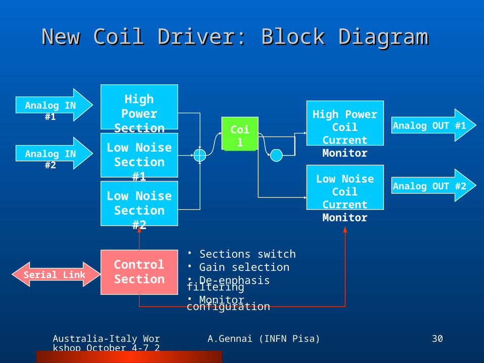
New Coil Driver: Block DiagramNew Coil Driver: Block Diagram
High Power Section
Low Noise Section #1
Low Noise Section #2
Analog IN #1
Analog IN #2
Control SectionSerial Link
Low Noise Coil Current
Monitor
High Power Coil Current
Monitor
Analog OUT #2
Analog OUT #1Coil
• Sections switch• Gain selection • De-enphasis filtering• Monitor configuration

Australia-Italy Workshop October 4-7 2005
A.Gennai (INFN Pisa) 31
Coil Drivers: Improved EMICoil Drivers: Improved EMI
High Power Section
Low Noise Section #1
Low Noise Section #2
Digital IN
Control Section
Serial Link
Low Noise Coil Current
Monitor
High Power Coil Current
Monitor
Digital OUT
Coil
• Sections switch• Gain selection • De-enphasis filtering• Monitor configuration
24bits DAC
24bits ADC
10 Mb/sec digital data electrically isolated
Digital IF
24bits DAC
24bits ADC

Australia-Italy Workshop October 4-7 2005
A.Gennai (INFN Pisa) 32
Coil Drivers: Preliminary LayoutCoil Drivers: Preliminary Layout
Control DAC / ADC (optional)
Analog Sections
Eurocard Module (3U)
Australia-Italy Workshop October 4-7 2005
A.Gennai (INFN Pisa) 33
New Digital to Analog Converter BoardNew Digital to Analog Converter Board
The need of a very high dynamical range for actuators has an impact also on digital to analog converter boards. The board currently in use has -98 dB of total harmonic distortion + noise while newer chips are available on market with –120 dB thus allowing a factor 10 gain in the DAC dynamical range.
Two different architectures:– Standard VME board, 16 ch. 24bits (nominal)– Distributed system
Australia-Italy Workshop October 4-7 2005
A.Gennai (INFN Pisa) 34
New Analog to Digital Converter BoardNew Analog to Digital Converter Board
Operation up to 100 kSamples/sec at very high resolution (24 bits nominal , 20 bit equivalent) (LAPP Annecy)– As for Digital-to-analog converters we are
investigating the possibility to distribute converters to front-end electronics to improve EMI.
2 MSamples/sec at lower resolution (16 bits nominal, 14 bit equivalent).– The goal is being able to replace any analog
control loop with a digital one:• Laser frequency stabilization.• Laser power stabilization.

Australia-Italy Workshop October 4-7 2005
A.Gennai (INFN Pisa) 35
ConclusionsConclusions
The new VIRGO control system, based on multi-DSP computing units, will allow operation up to 100 kSamples/sec at very high resolution (16 effective bits ADC, 20 effective bits DAC) and up to 2 MSamples/sec at lower resolution (14 effective bits ADC, 16-18 effective bits DAC) thus allowing extending applications range.
A first prototype of new multi-DSP board is currently under test in our lab.
Installation plan is quite complex.– Late 2006
• New DSP installation• New DAC and coil drivers electronics for payloads controls
– 2007• New ADC boards