the major cmos process technology changes from the 1980s to the 1990s
DESCRIPTION
ÂTRANSCRIPT

Hong Xiao, Ph. D. www2.austin.cc.tx.us/HongXiao/Book.htm 1
Chapter 14CMOS Processes
Hong Xiao, Ph. D.
www2.austin.cc.tx.us/HongXiao/Book.htm
Hong Xiao, Ph. D. www2.austin.cc.tx.us/HongXiao/Book.htm 2
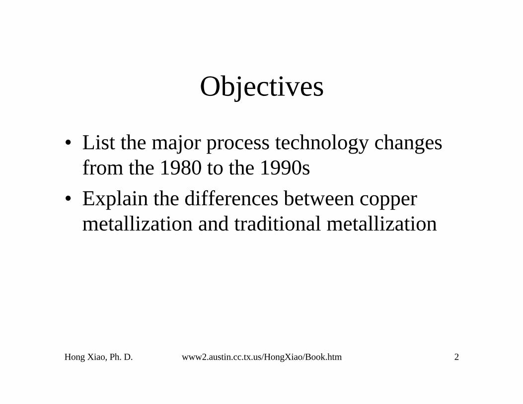
Objectives
• List the major process technology changesfrom the 1980 to the 1990s
• Explain the differences between coppermetallization and traditional metallization

Hong Xiao, Ph. D. www2.austin.cc.tx.us/HongXiao/Book.htm 3
From 1960s to 1970s
• 1960s– PMOS
– Diffusion
– Metal gate
• 1970s– NMOS
– Ion implantation
– Polysilicon gate

Hong Xiao, Ph. D. www2.austin.cc.tx.us/HongXiao/Book.htm 4
1980’s Technology
• LCD replacing LED as indicators forelectronic watches and calculators
• CMOS IC replacing NMOS IC for lowerpower consumption
• Minimum feature size: from 3 µm to 0.8 µm
• Wafer size: 100 mm (4 in) to 150 mm (6 in)
Hong Xiao, Ph. D. www2.austin.cc.tx.us/HongXiao/Book.htm 5
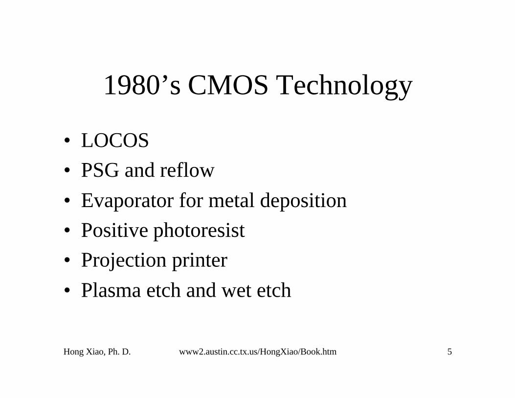
1980’s CMOS Technology
• LOCOS
• PSG and reflow
• Evaporator for metal deposition
• Positive photoresist
• Projection printer
• Plasma etch and wet etch

Hong Xiao, Ph. D. www2.austin.cc.tx.us/HongXiao/Book.htm 6
P-type substrate
1980’s Technology, Wafer Clean
Hong Xiao, Ph. D. www2.austin.cc.tx.us/HongXiao/Book.htm 7
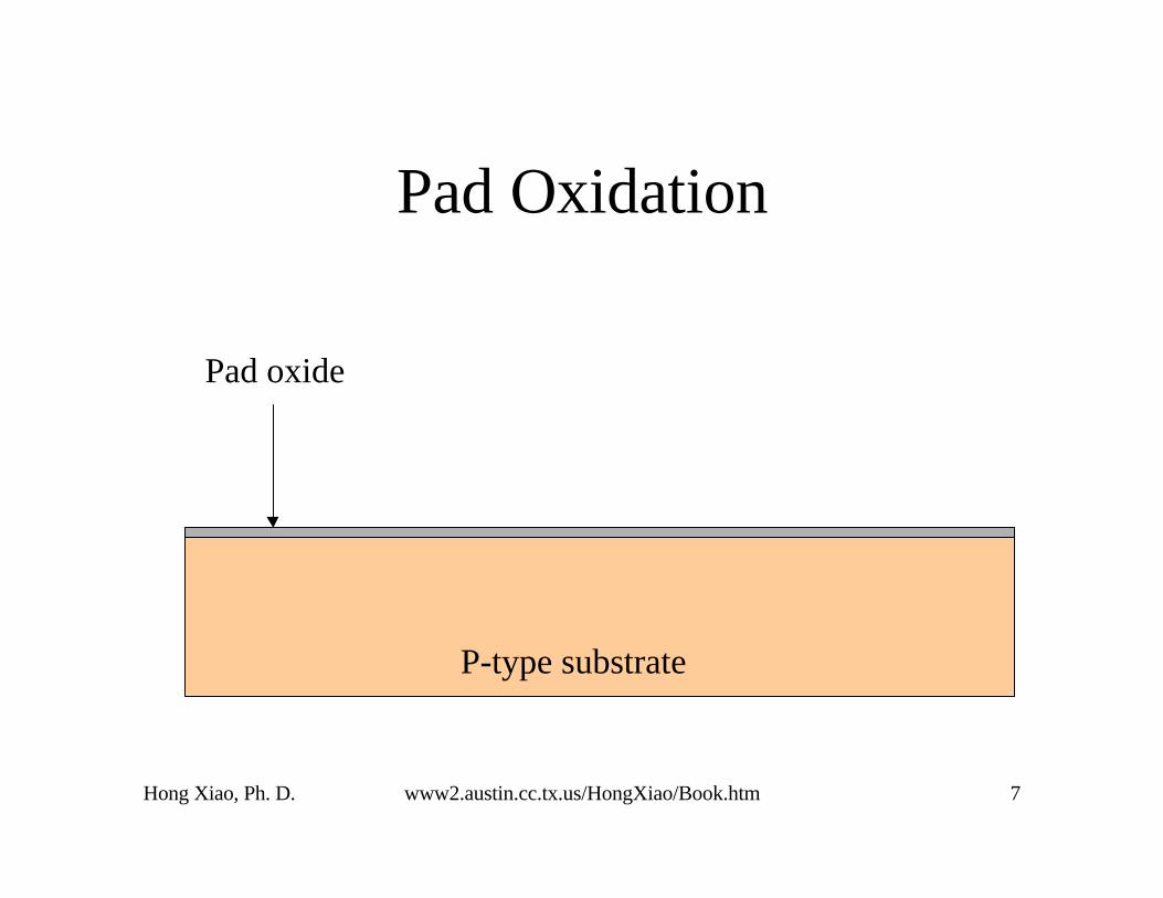
Pad oxide
P-type substrate
Pad Oxidation

Hong Xiao, Ph. D. www2.austin.cc.tx.us/HongXiao/Book.htm 8
Pad oxide
P-type substrate
Silicon nitride
LPCVD Nitride

Hong Xiao, Ph. D. www2.austin.cc.tx.us/HongXiao/Book.htm 9
Pad oxide
P-type substrate
PhotoresistSilicon nitride
Photoresist Coating

Hong Xiao, Ph. D. www2.austin.cc.tx.us/HongXiao/Book.htm 10
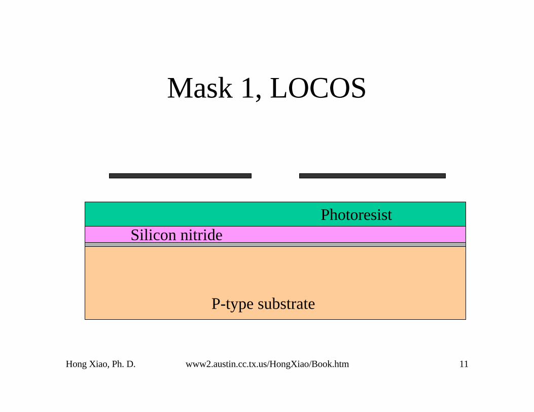
Mask 1, LOCOS
Hong Xiao, Ph. D. www2.austin.cc.tx.us/HongXiao/Book.htm 11
P-type substrate
PhotoresistSilicon nitride
Mask 1, LOCOS
Hong Xiao, Ph. D. www2.austin.cc.tx.us/HongXiao/Book.htm 12
P-type substrate
PhotoresistSilicon nitride
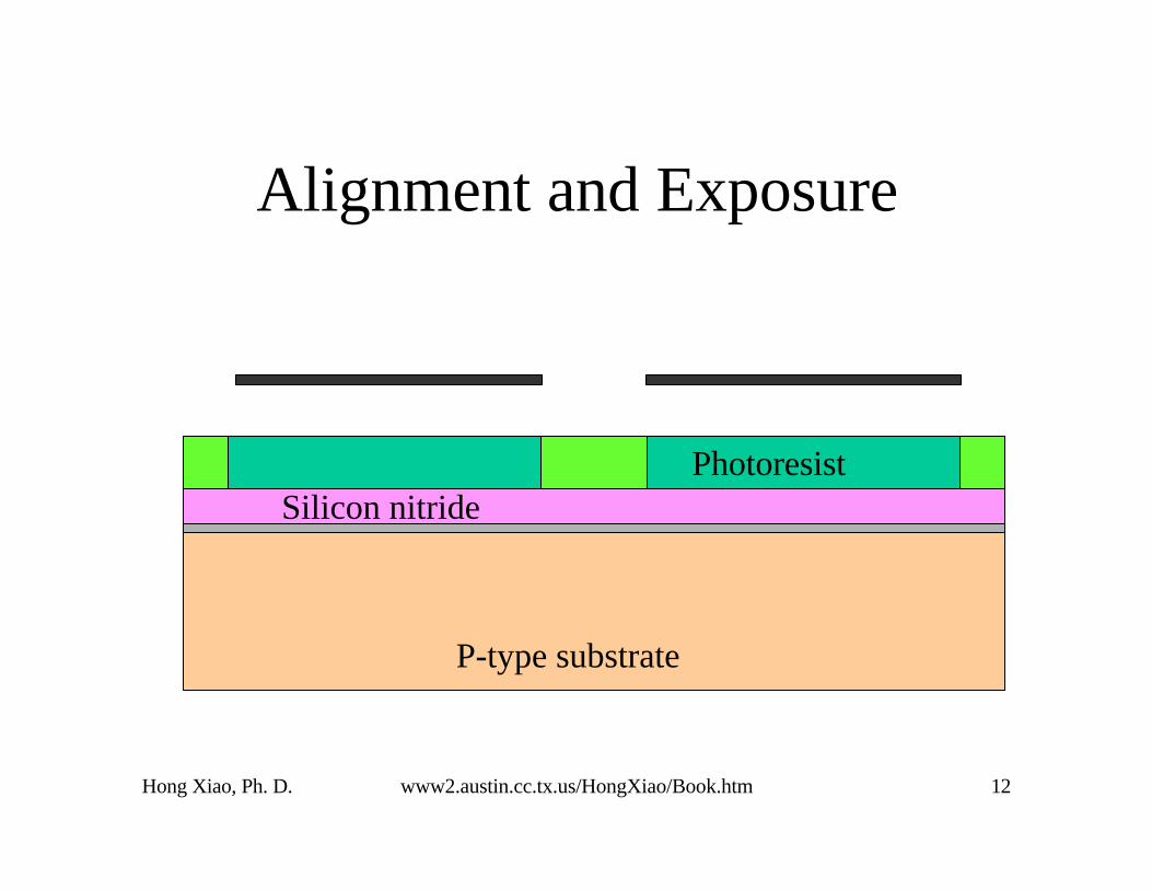
Alignment and Exposure
Hong Xiao, Ph. D. www2.austin.cc.tx.us/HongXiao/Book.htm 13
Silicon nitride
P-type substrate
Photoresist
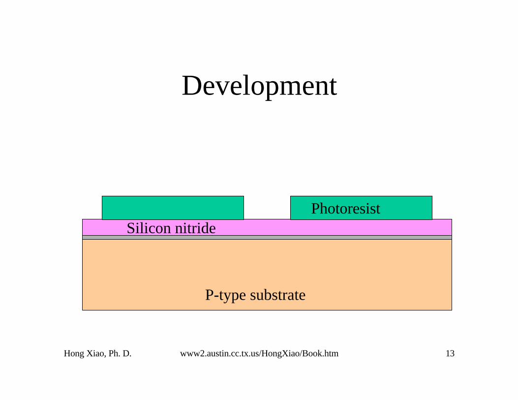
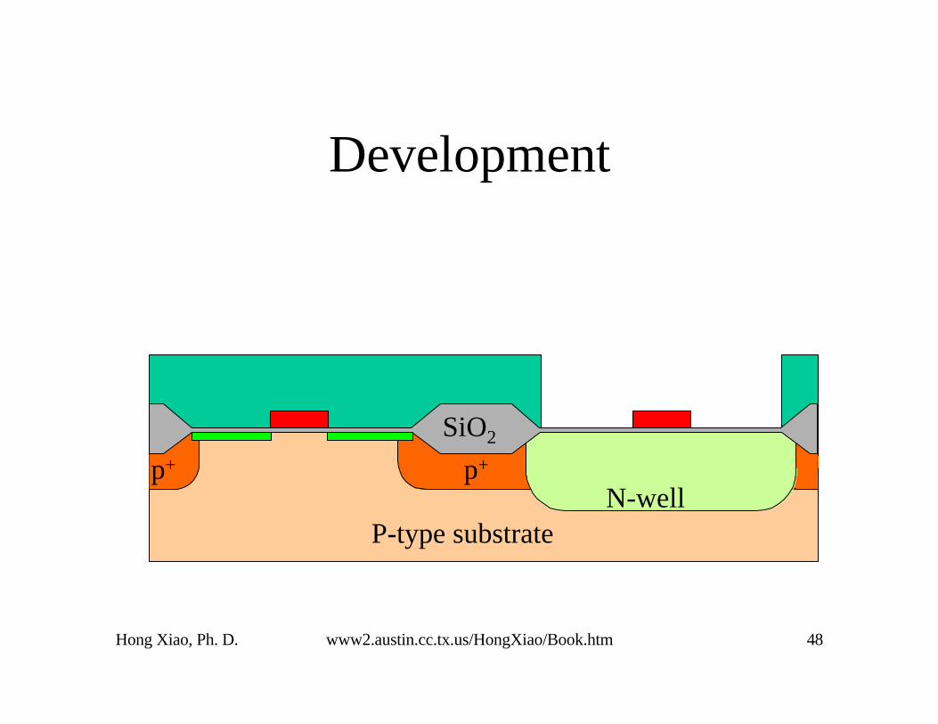
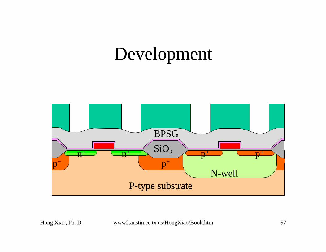
Development

Hong Xiao, Ph. D. www2.austin.cc.tx.us/HongXiao/Book.htm 14
Silicon nitride
P-type substrate
Photoresist
Etch Nitride
Hong Xiao, Ph. D. www2.austin.cc.tx.us/HongXiao/Book.htm 15
Silicon nitride
P-type substrate
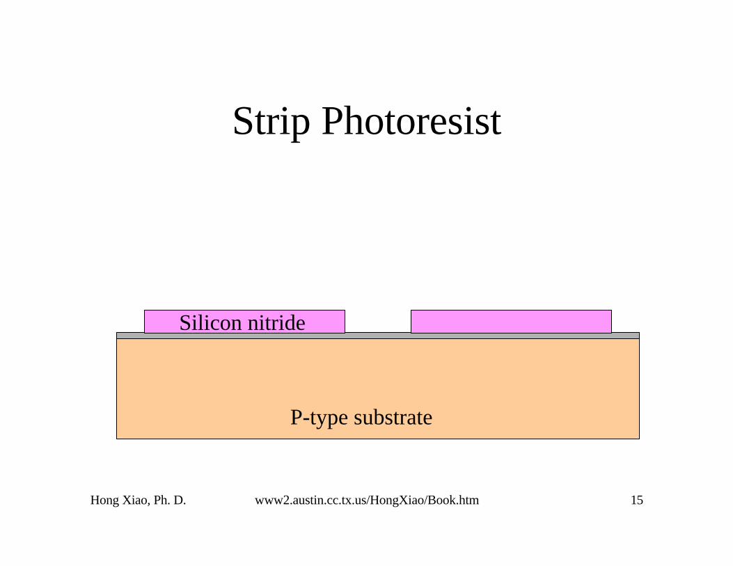
Strip Photoresist

Hong Xiao, Ph. D. www2.austin.cc.tx.us/HongXiao/Book.htm 16
Silicon nitride
P-type substrate
p+p+
Isolation Implantation

Hong Xiao, Ph. D. www2.austin.cc.tx.us/HongXiao/Book.htm 17
P-type substrate
Silicon nitride
p+p+
SiO2
LOCOS Oxidation

Hong Xiao, Ph. D. www2.austin.cc.tx.us/HongXiao/Book.htm 18
P-type substrate
p+p+
SiO2
Strip Nitride and Pad Oxide, Clean

Hong Xiao, Ph. D. www2.austin.cc.tx.us/HongXiao/Book.htm 19
P-type substrate
p+p+ p+
SiO2
Screen Oxidation

Hong Xiao, Ph. D. www2.austin.cc.tx.us/HongXiao/Book.htm 20
Photoresist
P-type substrate
p+p+ p+
SiO2
Photoresist Coating
Hong Xiao, Ph. D. www2.austin.cc.tx.us/HongXiao/Book.htm 21
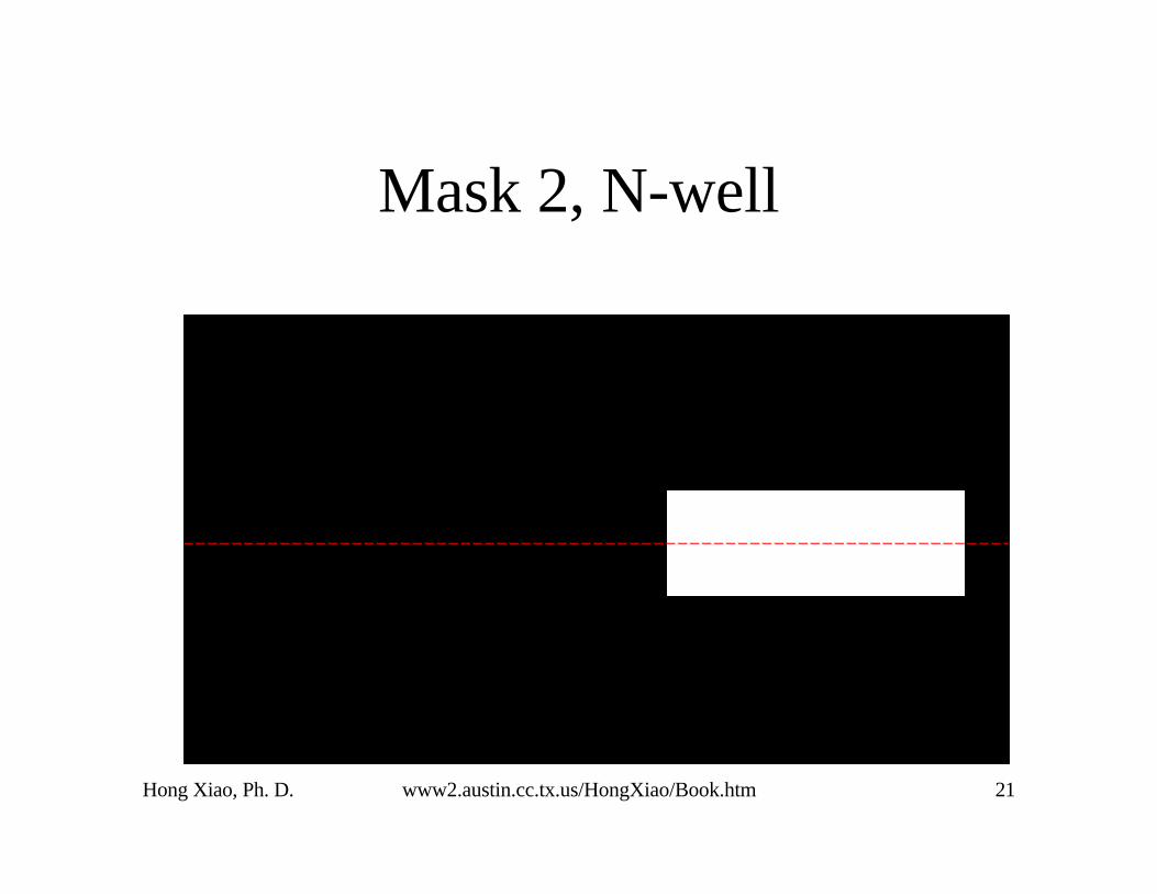
Mask 2, N-well
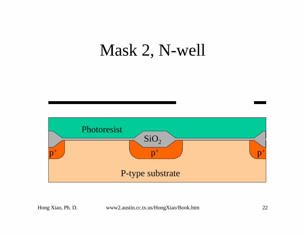
Hong Xiao, Ph. D. www2.austin.cc.tx.us/HongXiao/Book.htm 22
Photoresist
P-type substrate
p+p+ p+
SiO2
Mask 2, N-well
Hong Xiao, Ph. D. www2.austin.cc.tx.us/HongXiao/Book.htm 23
Photoresist
P-type substrate
p+p+ p+
SiO2
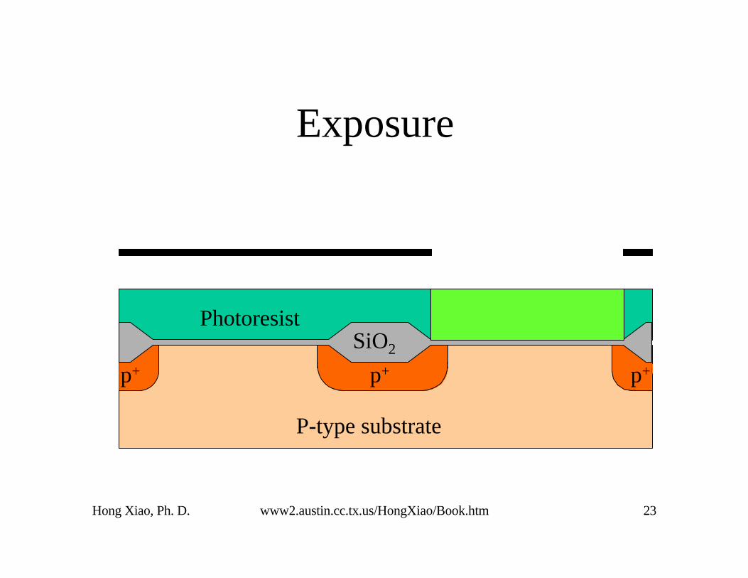
Exposure
Hong Xiao, Ph. D. www2.austin.cc.tx.us/HongXiao/Book.htm 24
Photoresist
P-type substrate
p+p+ p+
SiO2
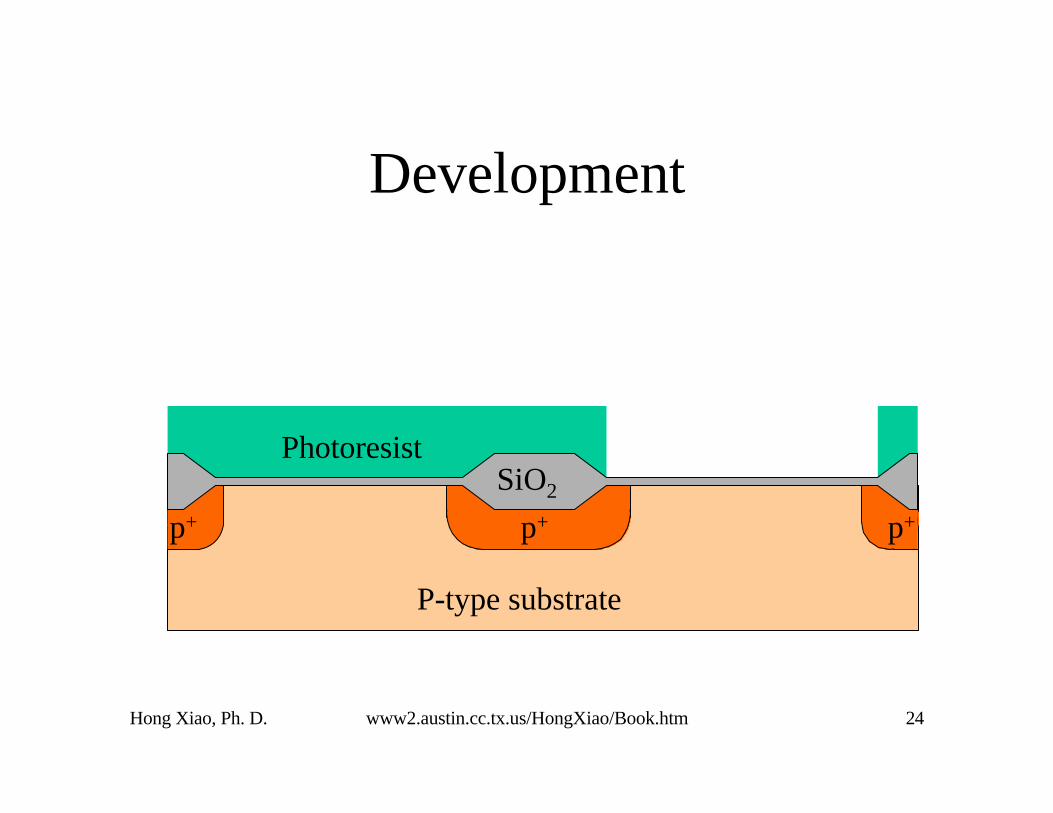
Development

Hong Xiao, Ph. D. www2.austin.cc.tx.us/HongXiao/Book.htm 25
Phosphorus Ions
Photoresist
P-type substrate
p+p+ p+
SiO2 N-well
N-well Implantation

Hong Xiao, Ph. D. www2.austin.cc.tx.us/HongXiao/Book.htm 26
P-type substrate
p+p+ p+
SiO2 N-well
Strip Photoresist
Hong Xiao, Ph. D. www2.austin.cc.tx.us/HongXiao/Book.htm 27
P-type substrate
p+p+
N-well
SiO2
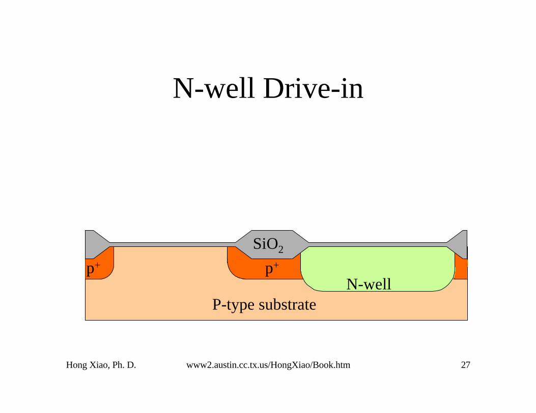
N-well Drive-in
Hong Xiao, Ph. D. www2.austin.cc.tx.us/HongXiao/Book.htm 28
P-type substrate
p+p+
N-well
SiO2
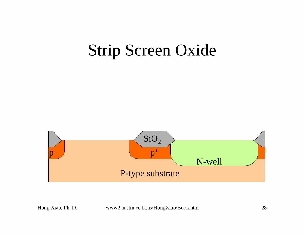
Strip Screen Oxide

Hong Xiao, Ph. D. www2.austin.cc.tx.us/HongXiao/Book.htm 29
P-type substrate
p+p+
N-well
SiO2
Grow Sacrificial Oxide
Hong Xiao, Ph. D. www2.austin.cc.tx.us/HongXiao/Book.htm 30
P-type substrate
p+p+
N-well
SiO2
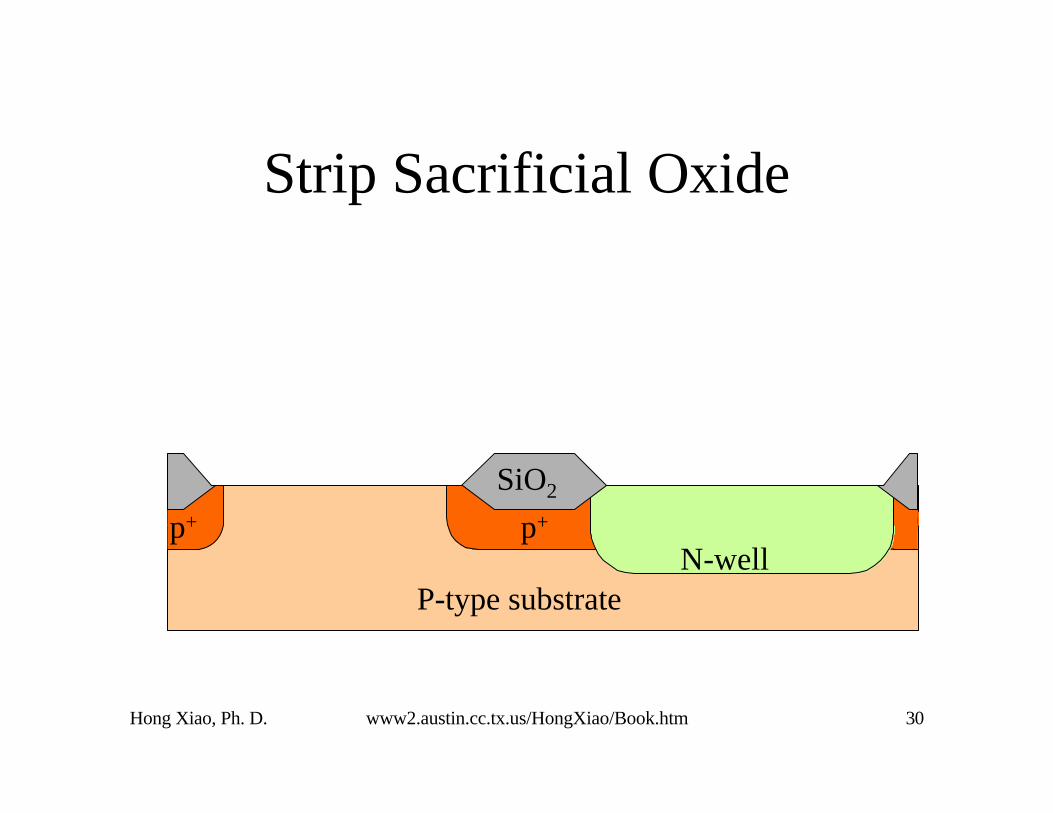
Strip Sacrificial Oxide

Hong Xiao, Ph. D. www2.austin.cc.tx.us/HongXiao/Book.htm 31
P-type substrate
p+p+
N-well
SiO2
Grow Gate Oxide

Hong Xiao, Ph. D. www2.austin.cc.tx.us/HongXiao/Book.htm 32
Polysilicon
P-type substrate
p+p+
N-well
SiO2
Gate Oxide
Deposit Polysilicon

Hong Xiao, Ph. D. www2.austin.cc.tx.us/HongXiao/Book.htm 33
Polysilicon
P-type substrate
p+p+
N-well
SiO2
Photoresist Coating
Hong Xiao, Ph. D. www2.austin.cc.tx.us/HongXiao/Book.htm 34
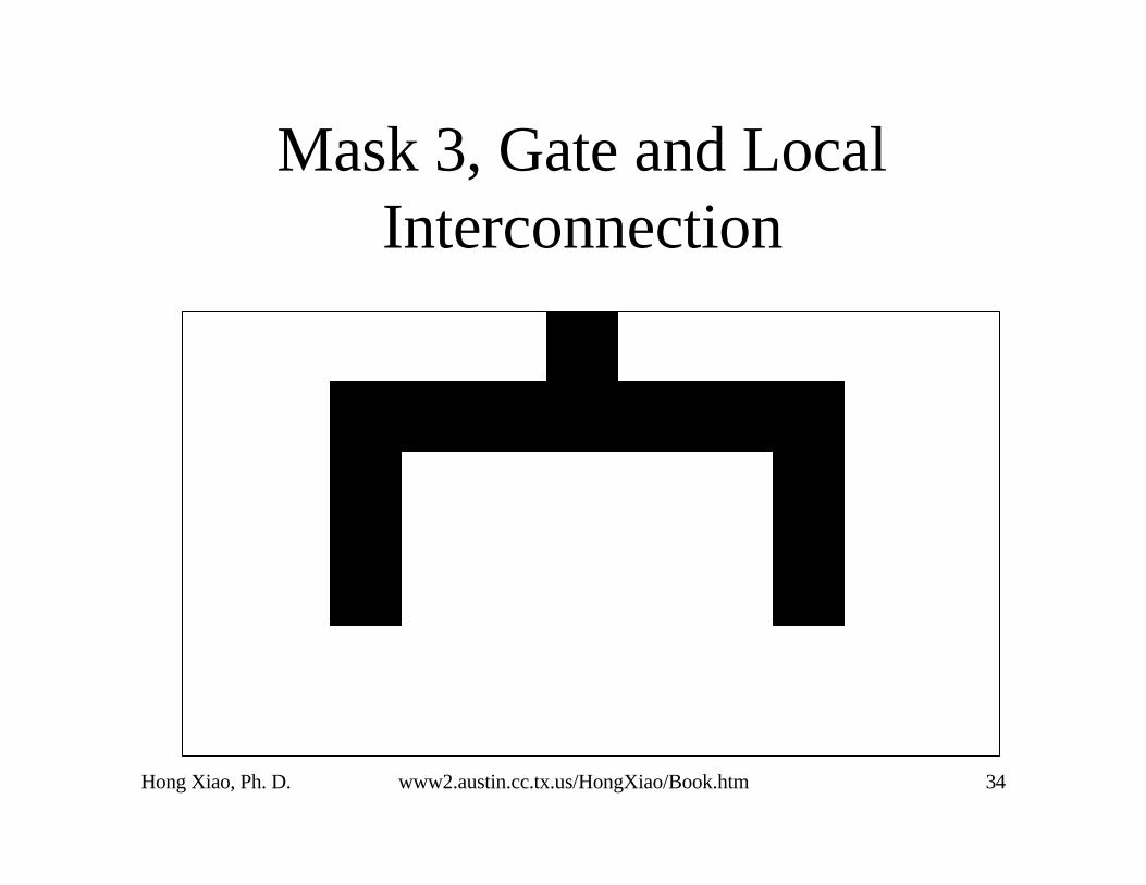
Mask 3, Gate and LocalInterconnection
Hong Xiao, Ph. D. www2.austin.cc.tx.us/HongXiao/Book.htm 35
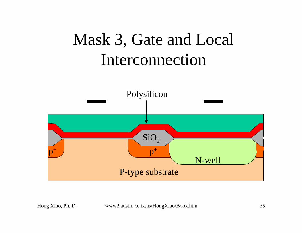
P-type substrate
p+p+
N-well
SiO2
Polysilicon
Mask 3, Gate and LocalInterconnection
Hong Xiao, Ph. D. www2.austin.cc.tx.us/HongXiao/Book.htm 36
Polysilicon
P-type substrate
p+p+
N-well
SiO2
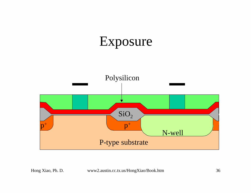
Exposure

Hong Xiao, Ph. D. www2.austin.cc.tx.us/HongXiao/Book.htm 37
Polysilicon
P-type substrate
p+p+
N-well
SiO2
Development

Hong Xiao, Ph. D. www2.austin.cc.tx.us/HongXiao/Book.htm 38
P-type substrate
p+p+
N-well
SiO2
PRPolysilicon Gate
Etch Polysilicon
Hong Xiao, Ph. D. www2.austin.cc.tx.us/HongXiao/Book.htm 39
Polysilicon
P-type substrate
p+p+
N-well
SiO2
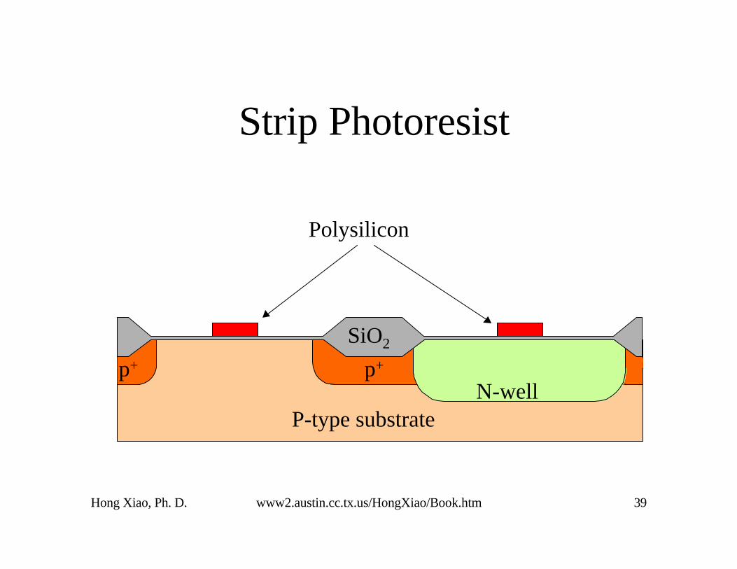
Strip Photoresist

Hong Xiao, Ph. D. www2.austin.cc.tx.us/HongXiao/Book.htm 40
Polysilicon
Photoresist
P-type substrate
p+p+
N-well
SiO2
Photoresist Coating
Hong Xiao, Ph. D. www2.austin.cc.tx.us/HongXiao/Book.htm 41
Photoresist
P-type substrate
p+p+
N-well
SiO2
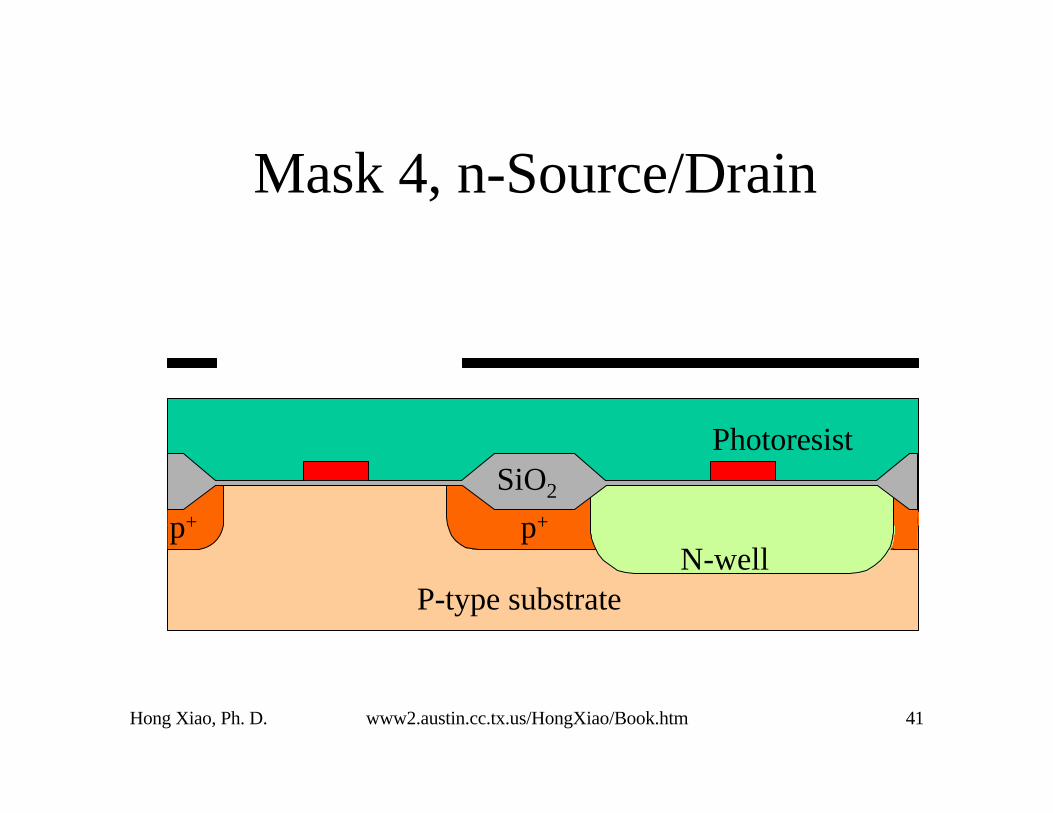
Mask 4, n-Source/Drain
Hong Xiao, Ph. D. www2.austin.cc.tx.us/HongXiao/Book.htm 42
Photoresist
P-type substrate
p+p+
N-well
SiO2
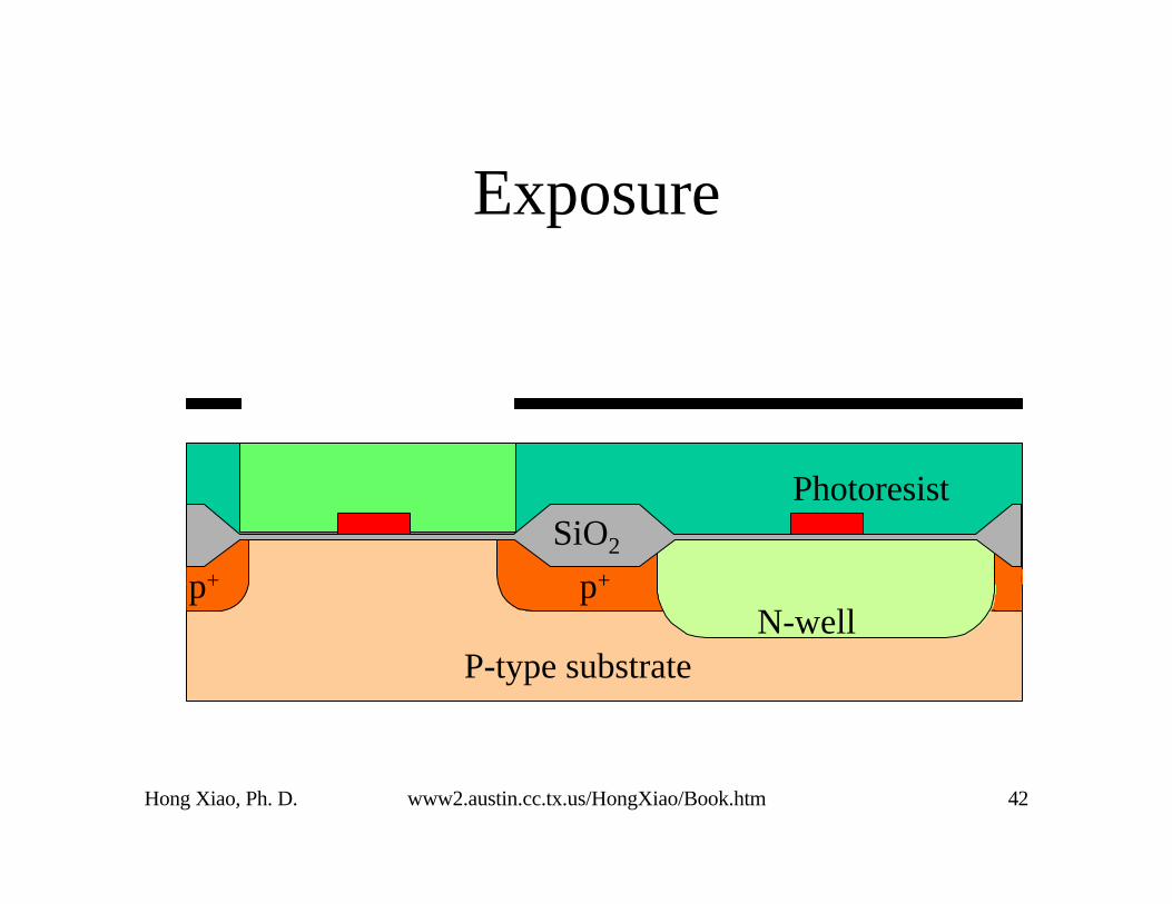
Exposure

Hong Xiao, Ph. D. www2.austin.cc.tx.us/HongXiao/Book.htm 43
Photoresist
P-type substrate
p+p+
N-well
SiO2
Development

Hong Xiao, Ph. D. www2.austin.cc.tx.us/HongXiao/Book.htm 44
Photoresist
P-type substrate
p+p+
N-well
SiO2
P+ implantation
N-Source/Drain Ion Implantation

Hong Xiao, Ph. D. www2.austin.cc.tx.us/HongXiao/Book.htm 45
Photoresist
P-type substrate
p+p+
N-well
SiO2
Strip Photoresist

Hong Xiao, Ph. D. www2.austin.cc.tx.us/HongXiao/Book.htm 46
P-type substrate
p+p+
N-well
SiO2
Photoresist Coating

Hong Xiao, Ph. D. www2.austin.cc.tx.us/HongXiao/Book.htm 47
P-type substrate
p+p+
N-well
SiO2
Mask 5, P-Source/Drain Exposure
Hong Xiao, Ph. D. www2.austin.cc.tx.us/HongXiao/Book.htm 48
P-type substrate
p+p+
N-well
SiO2
Development
Hong Xiao, Ph. D. www2.austin.cc.tx.us/HongXiao/Book.htm 49
B+ implantation
P-type substrate
p+p+
N-well
SiO2
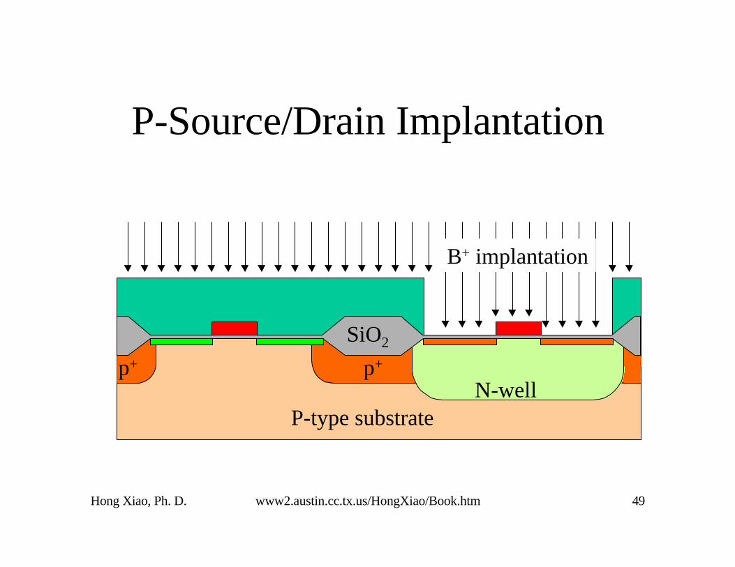
P-Source/Drain Implantation

Hong Xiao, Ph. D. www2.austin.cc.tx.us/HongXiao/Book.htm 50
P-type substrate
p+p+
N-well
SiO2
Strip Photoresist

Hong Xiao, Ph. D. www2.austin.cc.tx.us/HongXiao/Book.htm 51
P-type substrate
p+p+
N-wellP-type substrate
SiO2n+ n+ p+ p+
Anneal

Hong Xiao, Ph. D. www2.austin.cc.tx.us/HongXiao/Book.htm 52
P-type substrate
p+p+
N-wellP-type substrate
SiO2n+ n+ p+ p+
LPCVD Barrier Nitride

Hong Xiao, Ph. D. www2.austin.cc.tx.us/HongXiao/Book.htm 53
BPSG
P-type substrate
p+p+
N-wellP-type substrate
SiO2n+ n+ p+ p+
CVD BPSG

Hong Xiao, Ph. D. www2.austin.cc.tx.us/HongXiao/Book.htm 54
BPSG
P-type substrate
p+p+
N-wellP-type substrate
SiO2n+ n+ p+ p+
BPSG Reflow

Hong Xiao, Ph. D. www2.austin.cc.tx.us/HongXiao/Book.htm 55
BPSG
P-type substrate
p+p+
N-wellP-type substrate
SiO2n+ n+ p+ p+
Photoresist Coating

Hong Xiao, Ph. D. www2.austin.cc.tx.us/HongXiao/Book.htm 56
BPSG
P-type substrate
p+p+
N-wellP-type substrate
SiO2n+ n+ p+ p+
Mask 6, Contact Exposure
Hong Xiao, Ph. D. www2.austin.cc.tx.us/HongXiao/Book.htm 57
BPSG
P-type substrate
p+p+
N-wellP-type substrate
SiO2n+ n+ p+ p+
Development

Hong Xiao, Ph. D. www2.austin.cc.tx.us/HongXiao/Book.htm 58
BPSG
P-type substrate
p+p+
N-wellP-type substrate
SiO2n+ n+ p+ p+
Contact Etch

Hong Xiao, Ph. D. www2.austin.cc.tx.us/HongXiao/Book.htm 59
BPSG
P-type substrate
p+p+
N-wellP-type substrate
n+ n+ p+ p+SiO2
Strip Photoresist

Hong Xiao, Ph. D. www2.austin.cc.tx.us/HongXiao/Book.htm 60
Al·Cu·SiBPSG
P-type substrate
p+p+
N-wellP-type substrate
n+ n+ p+ p+SiO2
Metal Deposition

Hong Xiao, Ph. D. www2.austin.cc.tx.us/HongXiao/Book.htm 61
Al·Cu·SiBPSG
P-type substrate
p+p+
N-wellP-type substrate
n+ n+ p+ p+SiO2
Photoresist Coating

Hong Xiao, Ph. D. www2.austin.cc.tx.us/HongXiao/Book.htm 62
Al·Cu·SiBPSG
P-type substrate
p+p+
N-wellP-type substrate
n+ n+ p+ p+SiO2
Mask 7, Metal InterconnectionExposure

Hong Xiao, Ph. D. www2.austin.cc.tx.us/HongXiao/Book.htm 63
Al·Cu·SiBPSG
P-type substrate
p+p+
N-wellP-type substrate
n+ n+ p+ p+SiO2
Development

Hong Xiao, Ph. D. www2.austin.cc.tx.us/HongXiao/Book.htm 64
Al·Cu·SiBPSG
P-type substrate
p+p+
N-wellP-type substrate
n+ n+ p+ p+SiO2
Etch Metal
Hong Xiao, Ph. D. www2.austin.cc.tx.us/HongXiao/Book.htm 65
Al·Cu·SiBPSG
P-type substrate
p+p+
N-wellP-type substrate
n+ n+ p+ p+SiO2
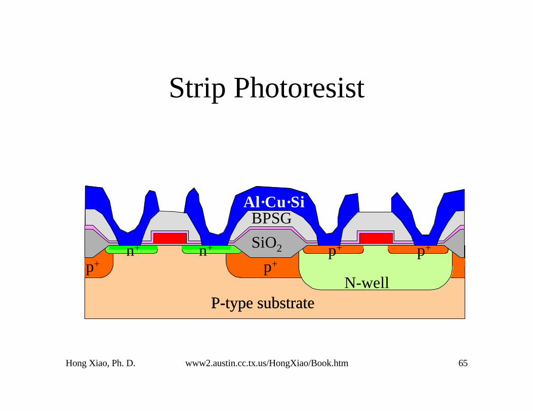
Strip Photoresist

Hong Xiao, Ph. D. www2.austin.cc.tx.us/HongXiao/Book.htm 66
USG
Al·Cu·SiBPSG
P-type substrate
p+p+
N-wellP-type substrate
n+ n+ p+ p+SiO2
CVD USG

Hong Xiao, Ph. D. www2.austin.cc.tx.us/HongXiao/Book.htm 67
USG
Al·Cu·SiBPSG
Nitride
P-type substrate
p+p+
N-wellP-type substrate
n+ n+ p+ p+SiO2
CVD Nitride
Hong Xiao, Ph. D. www2.austin.cc.tx.us/HongXiao/Book.htm 68
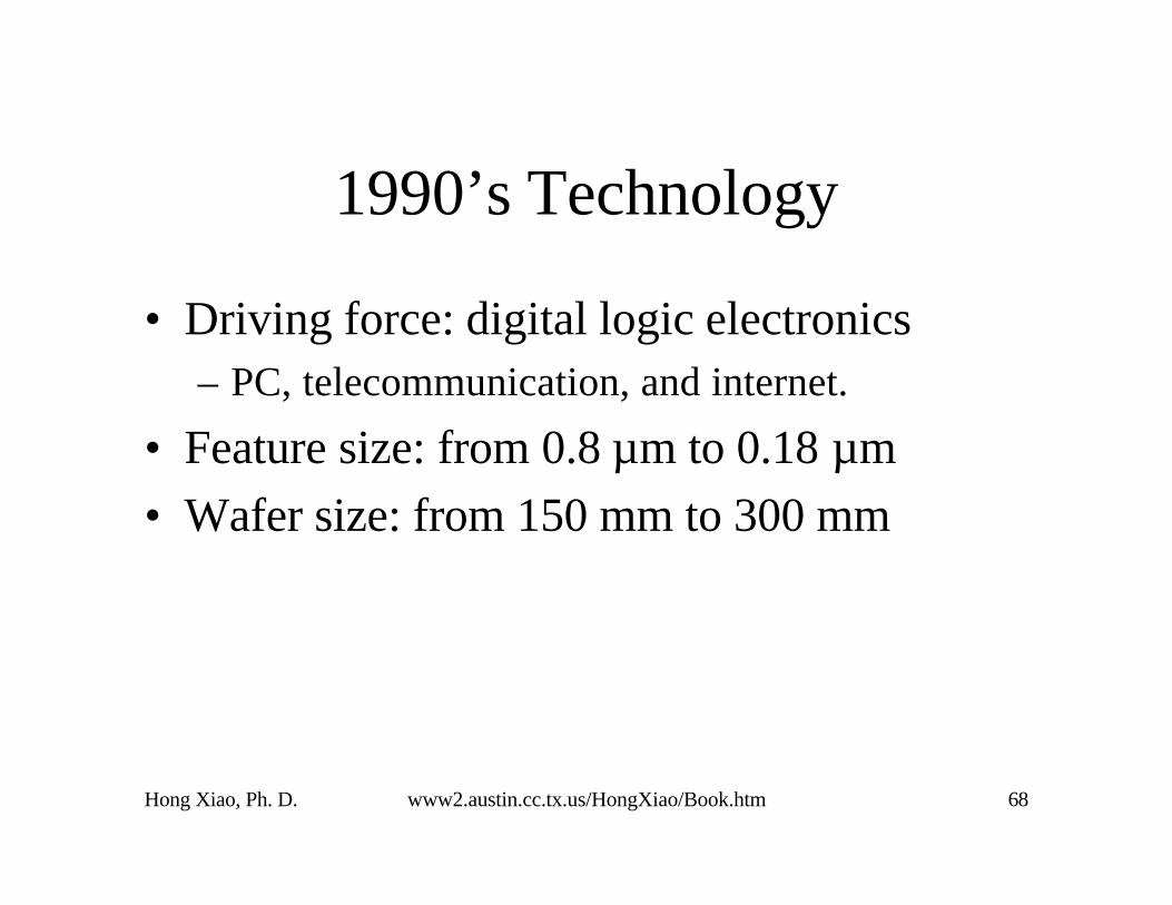
1990’s Technology
• Driving force: digital logic electronics– PC, telecommunication, and internet.
• Feature size: from 0.8 µm to 0.18 µm
• Wafer size: from 150 mm to 300 mm

Hong Xiao, Ph. D. www2.austin.cc.tx.us/HongXiao/Book.htm 69
1990’s CMOS Technology
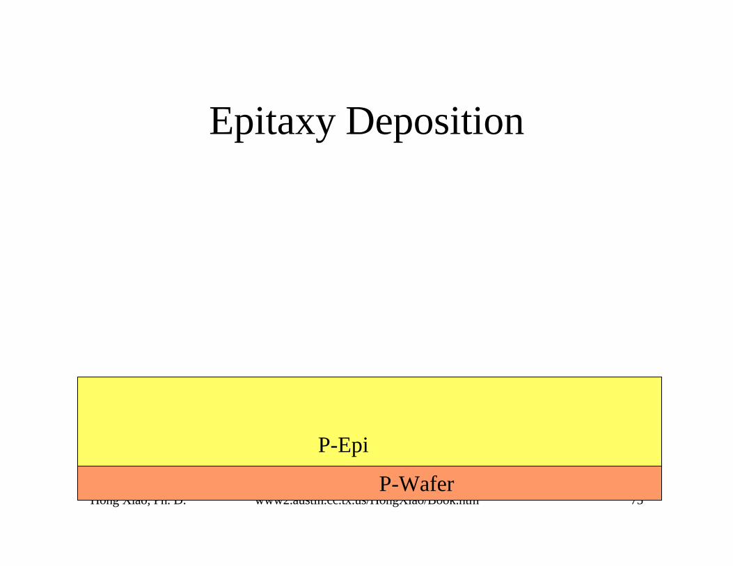
• Epitaxy silicon
• Shallow trench isolation
• The sidewall spacer for LDD and salicide
• Polycide gates and local interconnectionsreduce resistance and improve device speed– Tungsten silicide and titanium silicide.
Hong Xiao, Ph. D. www2.austin.cc.tx.us/HongXiao/Book.htm 70
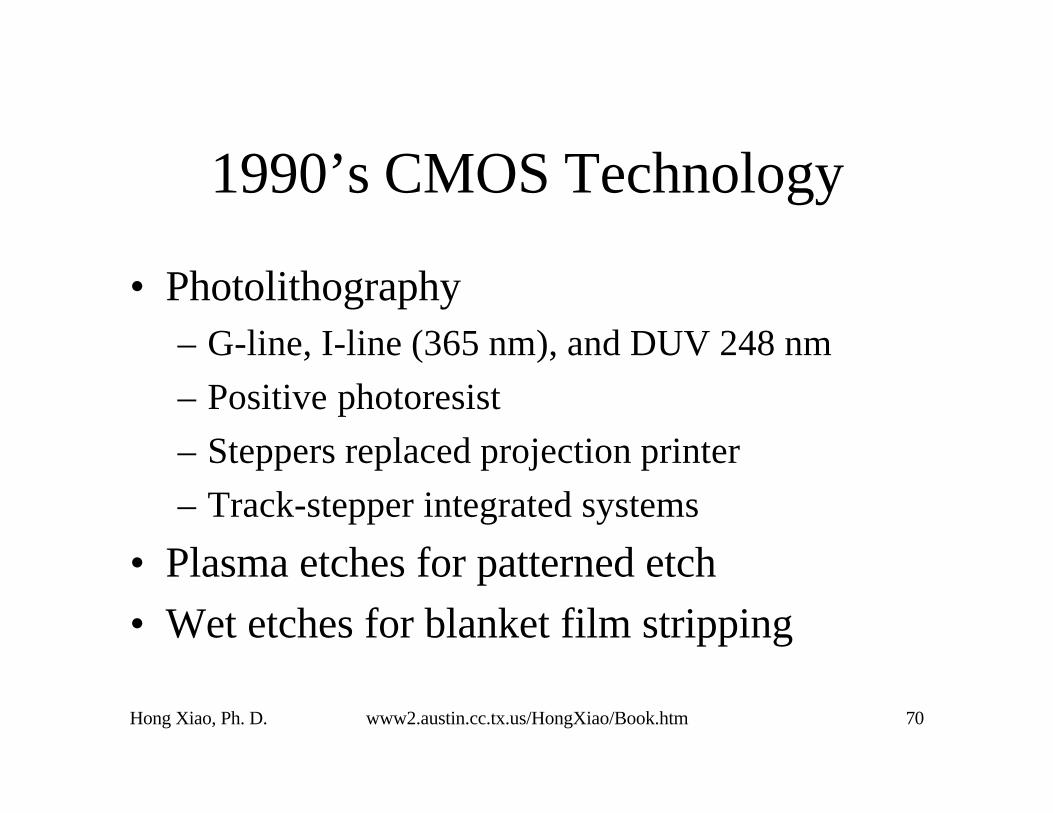
1990’s CMOS Technology
• Photolithography– G-line, I-line (365 nm), and DUV 248 nm
– Positive photoresist
– Steppers replaced projection printer
– Track-stepper integrated systems
• Plasma etches for patterned etch
• Wet etches for blanket film stripping
Hong Xiao, Ph. D. www2.austin.cc.tx.us/HongXiao/Book.htm 71
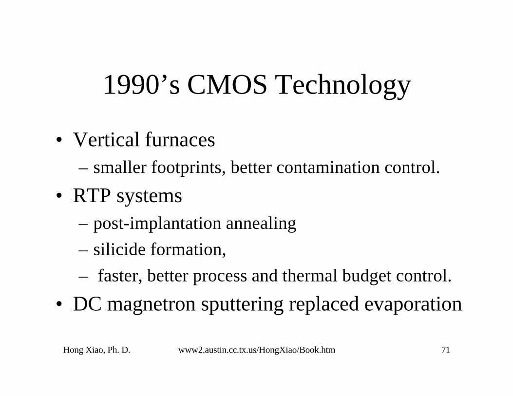
1990’s CMOS Technology
• Vertical furnaces– smaller footprints, better contamination control.
• RTP systems– post-implantation annealing
– silicide formation,
– faster, better process and thermal budget control.
• DC magnetron sputtering replaced evaporation
Hong Xiao, Ph. D. www2.austin.cc.tx.us/HongXiao/Book.htm 72
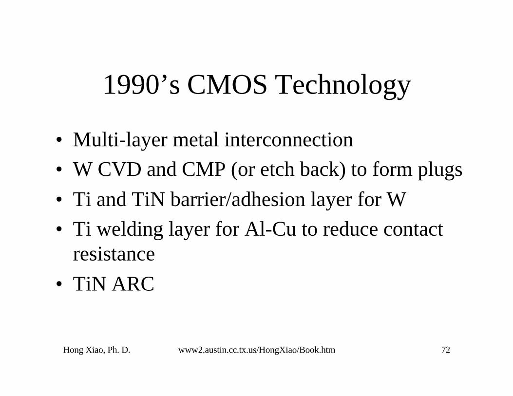
1990’s CMOS Technology
• Multi-layer metal interconnection
• W CVD and CMP (or etch back) to form plugs
• Ti and TiN barrier/adhesion layer for W
• Ti welding layer for Al-Cu to reduce contactresistance
• TiN ARC
Hong Xiao, Ph. D. www2.austin.cc.tx.us/HongXiao/Book.htm 73
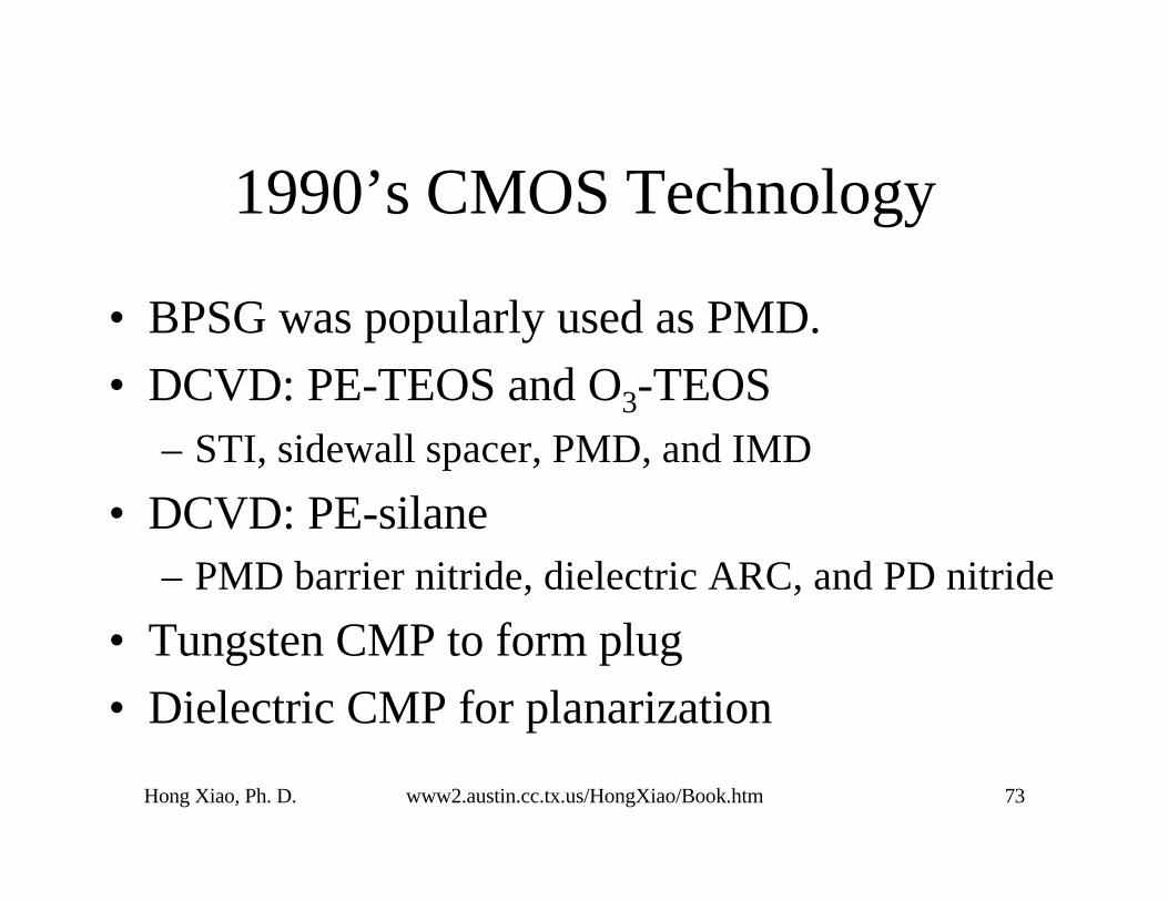
1990’s CMOS Technology
• BPSG was popularly used as PMD.
• DCVD: PE-TEOS and O3-TEOS– STI, sidewall spacer, PMD, and IMD
• DCVD: PE-silane– PMD barrier nitride, dielectric ARC, and PD nitride
• Tungsten CMP to form plug
• Dielectric CMP for planarization

Hong Xiao, Ph. D. www2.austin.cc.tx.us/HongXiao/Book.htm 74
1990’s CMOS Technology
• Cluster tools became very popular
• Single wafer processing systems improvewafer-to-wafer uniformity control
• Batch systems is still commonly employedin many non-critical processes for their highthroughput.
Hong Xiao, Ph. D. www2.austin.cc.tx.us/HongXiao/Book.htm 75
Epitaxy Deposition
P-Epi
P-Wafer

Hong Xiao, Ph. D. www2.austin.cc.tx.us/HongXiao/Book.htm 76
Mask 1: N-well

Hong Xiao, Ph. D. www2.austin.cc.tx.us/HongXiao/Book.htm 77
N-well Implantation
P-EpiP-Wafer
Photoresist
N-Well
Phosphorus Ions
Hong Xiao, Ph. D. www2.austin.cc.tx.us/HongXiao/Book.htm 78
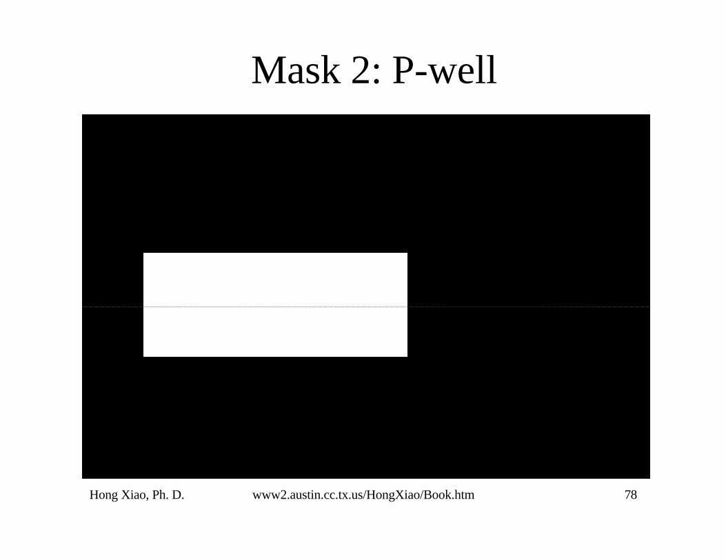
Mask 2: P-well

Hong Xiao, Ph. D. www2.austin.cc.tx.us/HongXiao/Book.htm 79
P-well Implantation
P-EpiP-Wafer
Boron Ions
P-WellN-Well
Photoresist

Hong Xiao, Ph. D. www2.austin.cc.tx.us/HongXiao/Book.htm 80
Strip PR, Strip Nitride/Pad Oxide
P-EpiP-Wafer
N-WellP-Well

Hong Xiao, Ph. D. www2.austin.cc.tx.us/HongXiao/Book.htm 81
Pad Oxidation, LPCVD Nitride
P-EpiP-Wafer
N-WellP-Well
Nitride

Hong Xiao, Ph. D. www2.austin.cc.tx.us/HongXiao/Book.htm 82
Mask 3: Shallow Trench Isolation

Hong Xiao, Ph. D. www2.austin.cc.tx.us/HongXiao/Book.htm 83
Etch Nitride, Pad Oxide and Silicon
P-EpiP-Wafer
N-WellP-Well
Nitride Nitride

Hong Xiao, Ph. D. www2.austin.cc.tx.us/HongXiao/Book.htm 84
HDP-CVD USG Trench Fill
P-EpiP-Wafer
N-WellP-Well
Nitride Nitride
USG
USG

Hong Xiao, Ph. D. www2.austin.cc.tx.us/HongXiao/Book.htm 85
CMP USG, Stop on Nitride
P-EpiP-Wafer
N-WellP-Well
Nitride Nitride
USG

Hong Xiao, Ph. D. www2.austin.cc.tx.us/HongXiao/Book.htm 86
Strip Nitride and Pad Oxide, Clean
P-EpiP-Wafer
N-WellP-Well
USGSTI

Hong Xiao, Ph. D. www2.austin.cc.tx.us/HongXiao/Book.htm 87
Mask 4: N-channel VT Adjust

Hong Xiao, Ph. D. www2.austin.cc.tx.us/HongXiao/Book.htm 88
Photoresist
Phosphorus Ions
P-EpiP-Wafer
N-WellP-Well
USGSTI

Hong Xiao, Ph. D. www2.austin.cc.tx.us/HongXiao/Book.htm 89
Mask 5: P-channel VT Adjust

Hong Xiao, Ph. D. www2.austin.cc.tx.us/HongXiao/Book.htm 90
Photoresist
Boron Ions
P-EpiP-Wafer
N-WellP-WellSTI USG
Hong Xiao, Ph. D. www2.austin.cc.tx.us/HongXiao/Book.htm 91
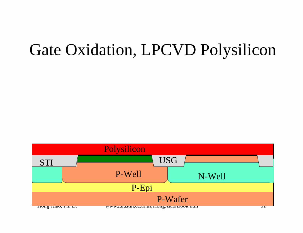
Gate Oxidation, LPCVD Polysilicon
Polysilicon
P-EpiP-Wafer
N-WellP-WellSTI USG

Hong Xiao, Ph. D. www2.austin.cc.tx.us/HongXiao/Book.htm 92
Mask 6: Gate & Local Interconnection
Hong Xiao, Ph. D. www2.austin.cc.tx.us/HongXiao/Book.htm 93
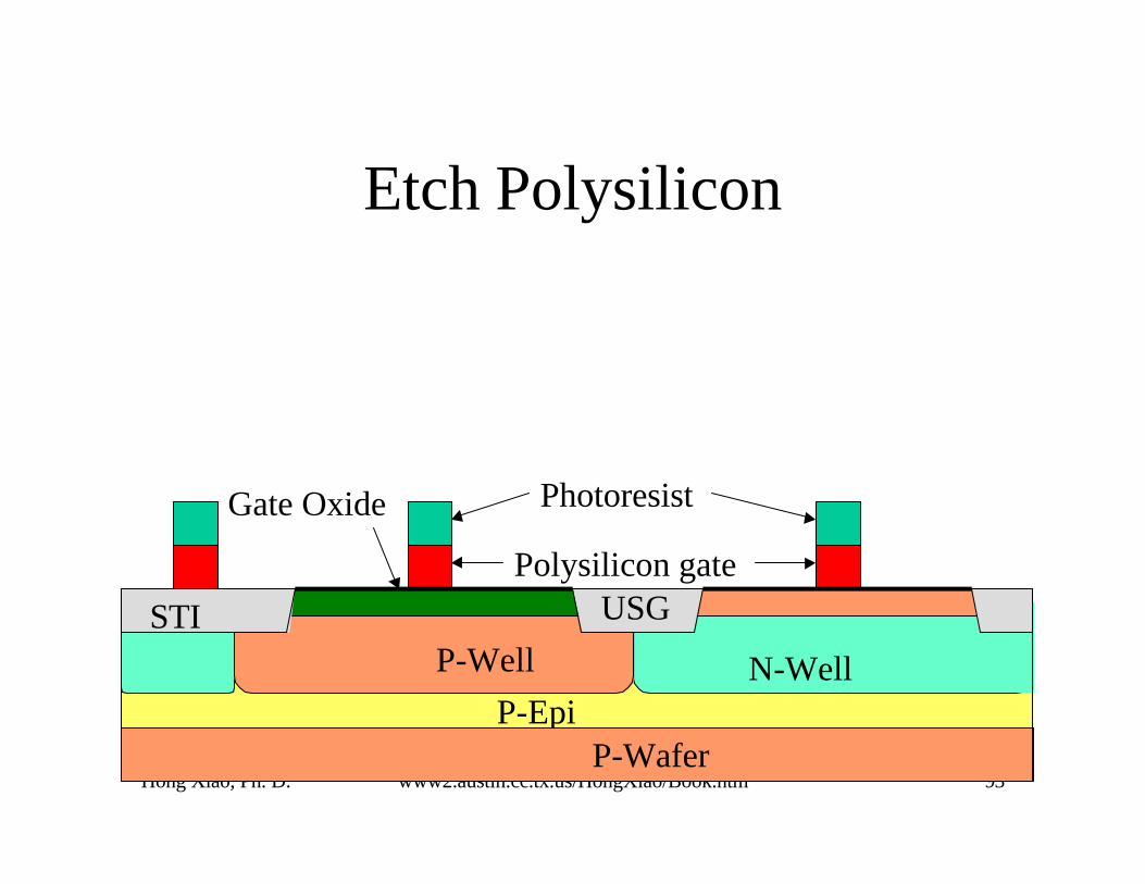
Etch Polysilicon
Polysilicon gate
P-EpiP-Wafer
N-WellP-WellSTI USG
PhotoresistGate Oxide

Hong Xiao, Ph. D. www2.austin.cc.tx.us/HongXiao/Book.htm 94
Mask 7: N-channel LDD

Hong Xiao, Ph. D. www2.austin.cc.tx.us/HongXiao/Book.htm 95
N-channel LDD Implantation, Arsenic
Photoresist
Arsenic Ions
P-EpiP-Wafer
N-WellP-Well
USGSTI
Hong Xiao, Ph. D. www2.austin.cc.tx.us/HongXiao/Book.htm 96
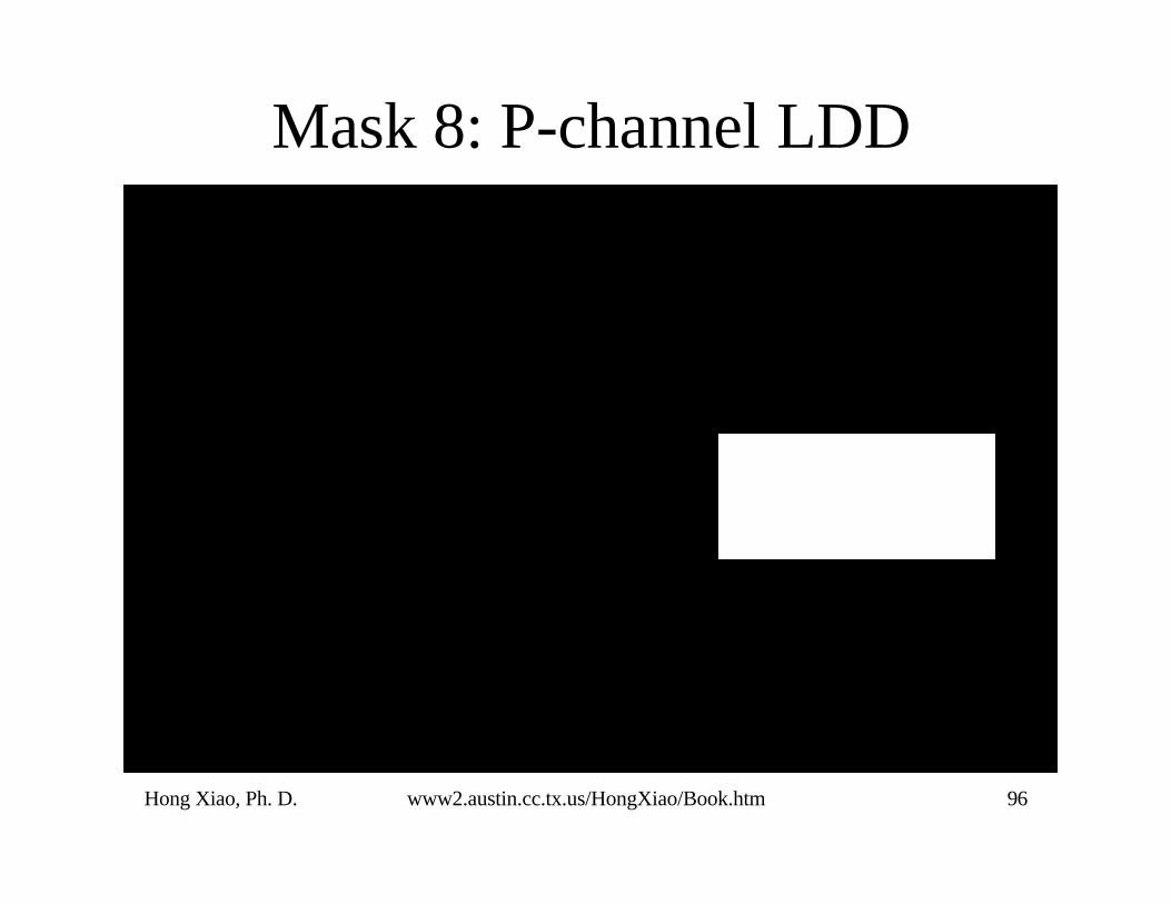
Mask 8: P-channel LDD
Hong Xiao, Ph. D. www2.austin.cc.tx.us/HongXiao/Book.htm 97
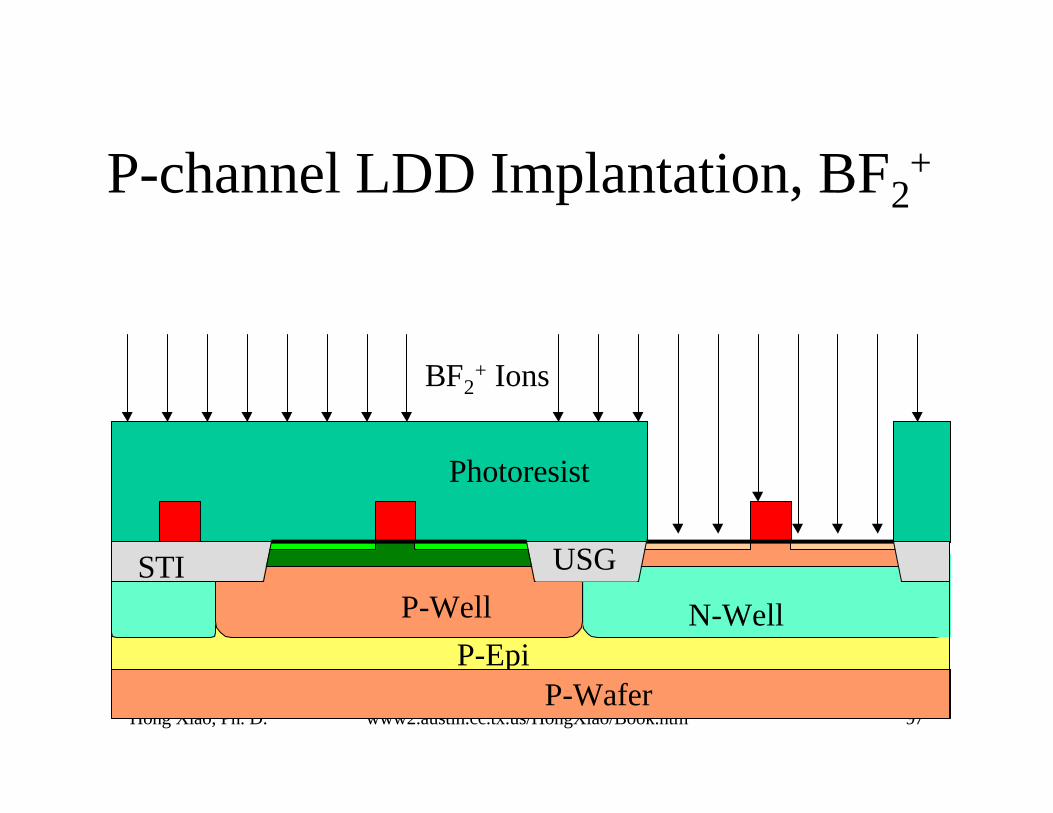
P-channel LDD Implantation, BF2+
Photoresist
BF2+ Ions
P-EpiP-Wafer
N-WellP-WellSTI USG

Hong Xiao, Ph. D. www2.austin.cc.tx.us/HongXiao/Book.htm 98
Sidewall Spacer
Gate oxiden- LDD n- LDD
SidewallSpacer
SidewallSpacer Polysilicon gatePolysilicon gate
Gate oxiden- LDD n- LDD
Hong Xiao, Ph. D. www2.austin.cc.tx.us/HongXiao/Book.htm 99
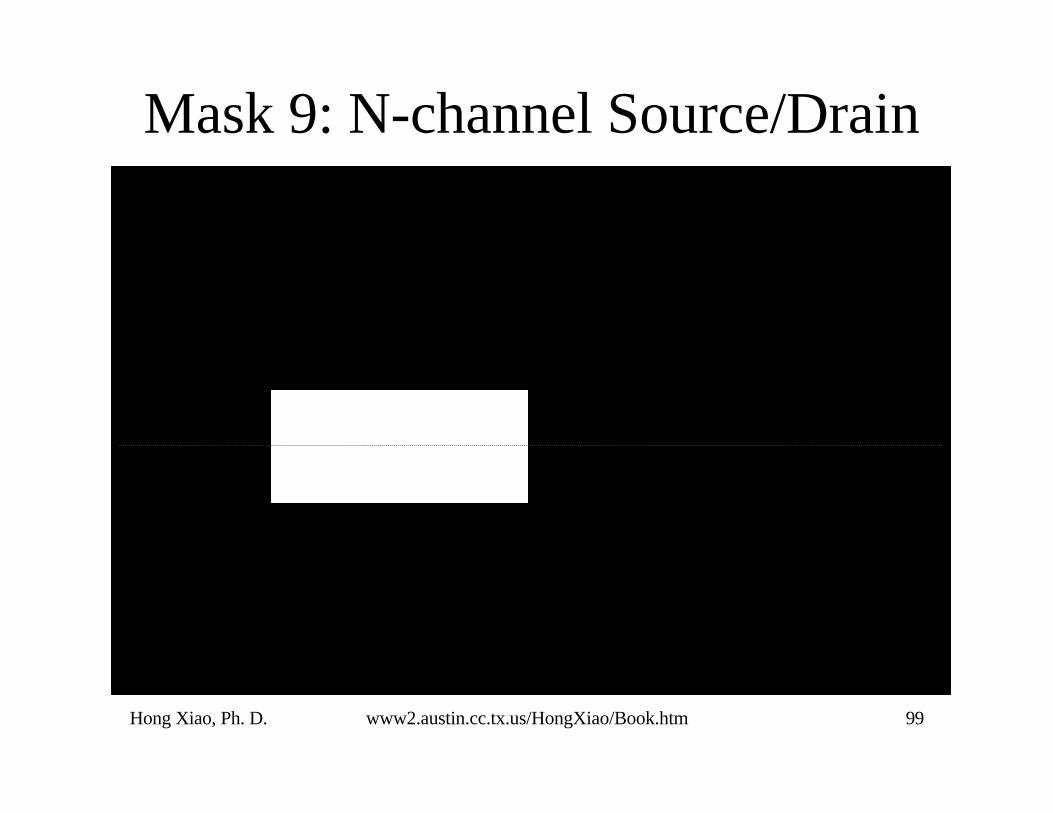
Mask 9: N-channel Source/Drain

Hong Xiao, Ph. D. www2.austin.cc.tx.us/HongXiao/Book.htm 100
N-channel Source/Drain Implantation
Photoresist
Phosphorus Ions
P-EpiP-Wafer
N-WellP-Well
n+n+STI p- p-USG

Hong Xiao, Ph. D. www2.austin.cc.tx.us/HongXiao/Book.htm 101
Mask 9: P-channel Source/Drain

Hong Xiao, Ph. D. www2.austin.cc.tx.us/HongXiao/Book.htm 102
P-channel Source/Drain Implantation
Photoresist
Boron Ions
P-EpiP-Wafer
N-WellP-Well
n+n+STI p+ p+USG
Hong Xiao, Ph. D. www2.austin.cc.tx.us/HongXiao/Book.htm 103
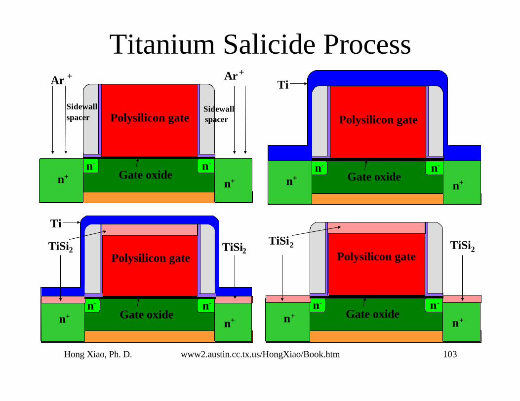
Titanium Salicide Process
Polysilicon gateSidewallspacer
Sidewallspacer
Gate oxiden- n-
n+n+
Ar + Ar+
Ti
Polysilicon gate
Gate oxiden- n-
n+n+
TiSi2 TiSi2
Ti
Polysilicon gate
Gate oxiden- n-
n+n+
TiSi2 TiSi2Polysilicon gate
Gate oxiden- n-
n+n+

Hong Xiao, Ph. D. www2.austin.cc.tx.us/HongXiao/Book.htm 104
Titanium Self-aligned silicide Process
Titanium Deposition
RTP Silicide Alloying
Strip Unreact Titanium
Silicon
Silicon
Silicon
STI
Sidewall Spacer
Titanium
Titanium SilicidePolysilicon
Gate Oxide

Hong Xiao, Ph. D. www2.austin.cc.tx.us/HongXiao/Book.htm 105
BPSG Deposition and Reflow
n+n+ p+ p+STI USG
BPSG
n+n+ p+ p+STI USG
BPSG

Hong Xiao, Ph. D. www2.austin.cc.tx.us/HongXiao/Book.htm 106
Mask 10: Contact Hole

Hong Xiao, Ph. D. www2.austin.cc.tx.us/HongXiao/Book.htm 107
Contact Hole Etch, BPSG Etch
P-EpiP-Wafer
N-WellP-Well
BPSG
n+n+ p+ p+STI USG
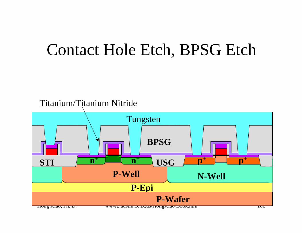
Hong Xiao, Ph. D. www2.austin.cc.tx.us/HongXiao/Book.htm 108
Contact Hole Etch, BPSG Etch
P-EpiP-Wafer
N-WellP-Well
BPSG
n+n+ p+ p+STI USG
Tungsten
Titanium/Titanium Nitride

Hong Xiao, Ph. D. www2.austin.cc.tx.us/HongXiao/Book.htm 109
Contact Hole Etch, BPSG Etch
P-EpiP-Wafer
N-WellP-Well
BPSG
n+n+ p+ p+STI USG
Titanium/Titanium Nitride
Aluminum Copper Alloy
TitaniumTiN ARC
W

Hong Xiao, Ph. D. www2.austin.cc.tx.us/HongXiao/Book.htm 110
Mask 11: Metal 1 Interconnect

Hong Xiao, Ph. D. www2.austin.cc.tx.us/HongXiao/Book.htm 111
Metal Etch
P-EpiP-Wafer
N-WellP-Well
BPSG
n+n+ p+ p+STI USG
Titanium/Titanium Nitride TitaniumTiN ARC
W
Al-Cu Alloy

Hong Xiao, Ph. D. www2.austin.cc.tx.us/HongXiao/Book.htm 112
PE-TEOS USG Dep/Etch/Dep/CMP
P-EpiP-Wafer
N-WellP-Well
BPSG
n+n+ p+ p+STI USG
W
Al-Cu Alloy
USG Dep/Etch/Dep/CMPIMD 1

Hong Xiao, Ph. D. www2.austin.cc.tx.us/HongXiao/Book.htm 113
Mask 12: Via 1

Hong Xiao, Ph. D. www2.austin.cc.tx.us/HongXiao/Book.htm 114
Via Etch, Etch USG
P-EpiP-Wafer
N-WellP-Well
BPSG
n+n+ p+ p+STI USG
W
Al-Cu Alloy
USGIMD 1

Hong Xiao, Ph. D. www2.austin.cc.tx.us/HongXiao/Book.htm 115
Via Etch, Etch USG
P-EpiP-Wafer
N-WellP-Well
BPSG
n+n+ p+ p+STI USG
W
Al-Cu Alloy
USG
Metal 2 Al-Cu Alloy
M1
IMD 1

Hong Xiao, Ph. D. www2.austin.cc.tx.us/HongXiao/Book.htm 116
Mask 13: Metal 2 Interconnect
Hong Xiao, Ph. D. www2.austin.cc.tx.us/HongXiao/Book.htm 117
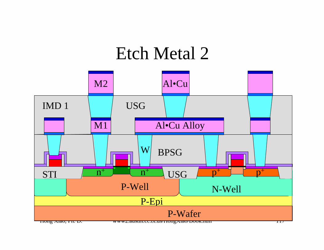
Etch Metal 2
P-EpiP-Wafer
N-WellP-Well
BPSG
n+n+ p+ p+STI USG
W
Al•Cu Alloy
USG
M1
M2 Al•Cu
IMD 1

Hong Xiao, Ph. D. www2.austin.cc.tx.us/HongXiao/Book.htm 118
USG Dep/Etch/Dep/CMP
P-EpiP-Wafer
N-WellP-Well
BPSG
n+n+ p+ p+STI USG
W
Al•Cu Alloy
USG
M1
M2 Al•Cu
USG
IMD 1
IMD 2

Hong Xiao, Ph. D. www2.austin.cc.tx.us/HongXiao/Book.htm 119
Mask 14: Via 2
Hong Xiao, Ph. D. www2.austin.cc.tx.us/HongXiao/Book.htm 120
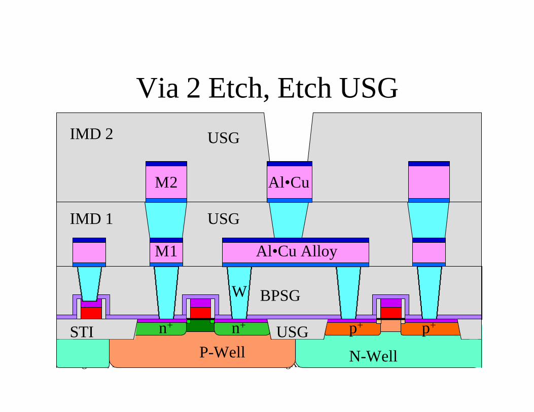
Via 2 Etch, Etch USG
N-WellP-Well
BPSG
n+n+ p+ p+STI USG
W
Al•Cu Alloy
USG
M1
M2 Al•Cu
USG
IMD 1
IMD 2

Hong Xiao, Ph. D. www2.austin.cc.tx.us/HongXiao/Book.htm 121
Metallization of Metal 3
N-WellP-Well
BPSG
n+n+ p+ p+STI USG
W
Al•Cu Alloy
USG
M1
M2 Al•Cu
USG
Metal 3 Al•Cu Alloy
W
IMD 1
IMD 2

Hong Xiao, Ph. D. www2.austin.cc.tx.us/HongXiao/Book.htm 122
Mask 15: Metal 3 Interconnects

Hong Xiao, Ph. D. www2.austin.cc.tx.us/HongXiao/Book.htm 123
Metal Etch, PR Strip and Metal Anneal
N-WellP-Well
BPSG
p+ p+STI USG
W
Al•Cu Alloy
USG
M1
M2 Al•Cu
USG
Metal 3 Al•Cu Alloy
W
IMD 1
IMD 2
n+n+

Hong Xiao, Ph. D. www2.austin.cc.tx.us/HongXiao/Book.htm 124
PE-TEOS USG Dep/Etch/Dep/CMP
Al•Cu Alloy
USG
M1
M2 Al•Cu
USG
Metal 3 Al•Cu Alloy
W
USG
IMD 1
IMD 2
IMD 3

Hong Xiao, Ph. D. www2.austin.cc.tx.us/HongXiao/Book.htm 125
Mask 16: Via 3

Hong Xiao, Ph. D. www2.austin.cc.tx.us/HongXiao/Book.htm 126
Via 3 Etch and PR Strip
Al•Cu Alloy
USG
M1
M2 Al•Cu
USG
Metal 3 Al•Cu Alloy
W
IMD 1
IMD 2
IMD 3 USG

Hong Xiao, Ph. D. www2.austin.cc.tx.us/HongXiao/Book.htm 127
Metal 4 Deposition
Al•Cu Alloy
USG
M1
M2 Al•Cu
USG
Metal 3 Al•Cu Alloy
W
IMD 1
IMD 2
IMD 3 USGMetal 4
Al•Cu
Hong Xiao, Ph. D. www2.austin.cc.tx.us/HongXiao/Book.htm 128
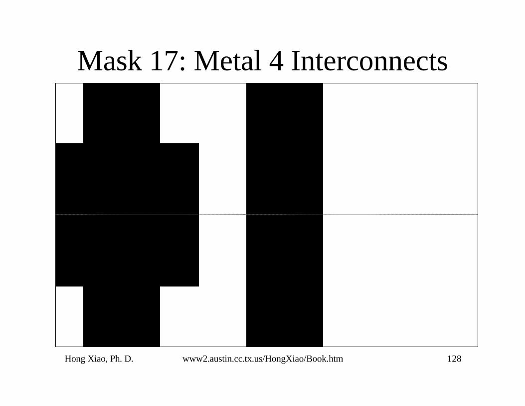
Mask 17: Metal 4 Interconnects
Hong Xiao, Ph. D. www2.austin.cc.tx.us/HongXiao/Book.htm 129
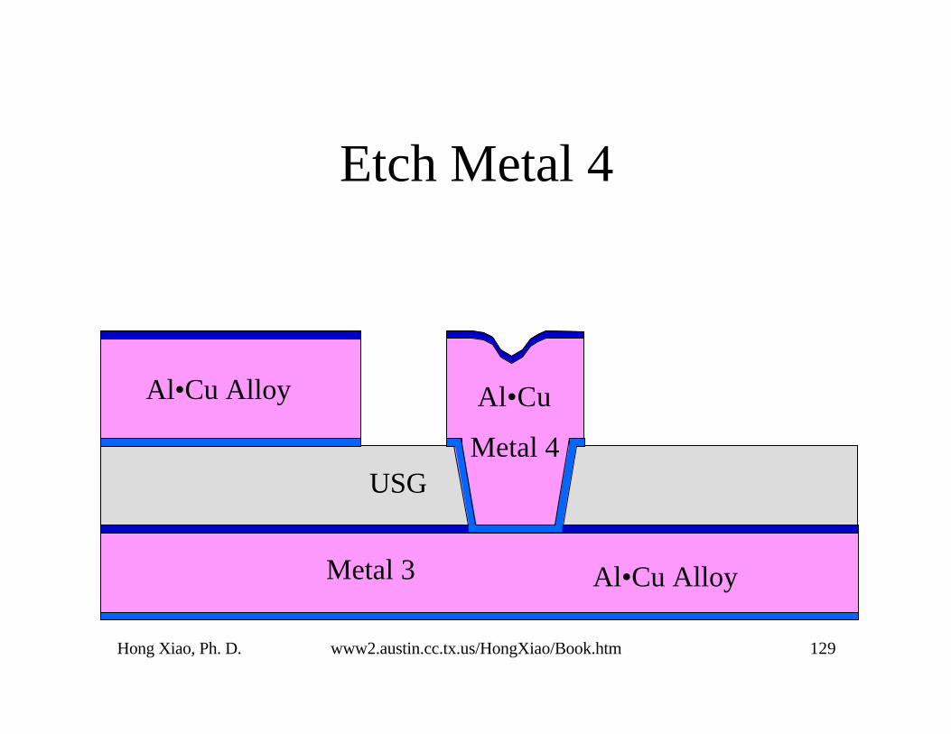
Etch Metal 4
Metal 3 Al•Cu Alloy
IMD 3 USGMetal 4
Al•CuAl•Cu Alloy

Hong Xiao, Ph. D. www2.austin.cc.tx.us/HongXiao/Book.htm 130
Passivation Dielectric Deposition
Metal 3 Al•Cu Alloy
IMD 3 USGMetal 4
Al•Cu
USG
Al•Cu Alloy
Silicon Nitride

Hong Xiao, Ph. D. www2.austin.cc.tx.us/HongXiao/Book.htm 131
Mask 18: Bonding Pad
Hong Xiao, Ph. D. www2.austin.cc.tx.us/HongXiao/Book.htm 132
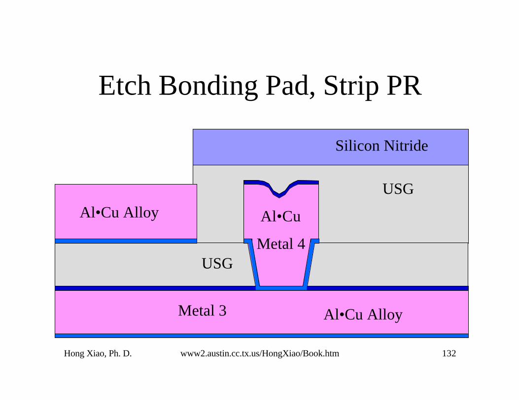
Etch Bonding Pad, Strip PR
Metal 3 Al•Cu Alloy
IMD 3 USGMetal 4
Al•Cu
USG
Silicon Nitride
Al•Cu Alloy
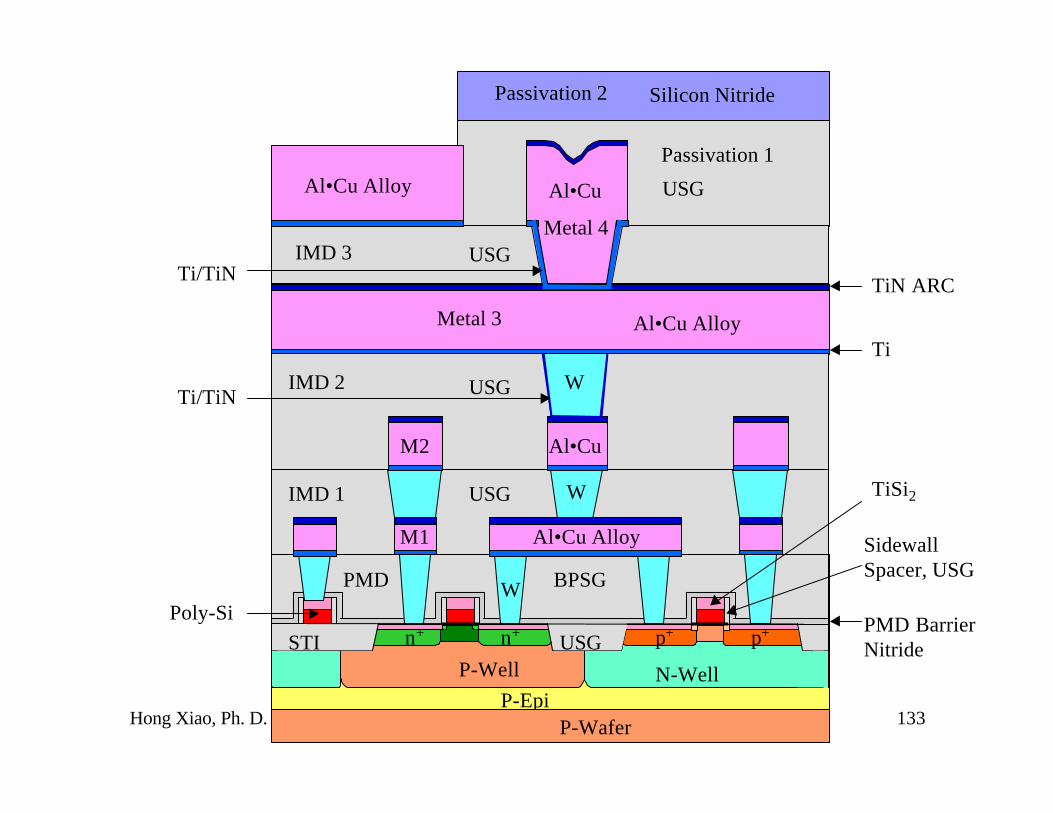
Hong Xiao, Ph. D. www2.austin.cc.tx.us/HongXiao/Book.htm 133P-Epi
P-Wafer
Metal 3 Al•Cu Alloy
IMD 3 USGMetal 4
Al•Cu USG
Silicon Nitride
Al•Cu Alloy
N-WellP-Well
BPSG
n+n+ p+ p+STI USG
W
Al•Cu Alloy
USG
M1
M2 Al•Cu
USG W
IMD 1
IMD 2
TiSi2
Poly-Si
Ti
TiN ARC
W
Ti/TiN
Ti/TiN
SidewallSpacer, USG
PMD BarrierNitride
IMD 3
Passivation 1
Passivation 2
PMD

Hong Xiao, Ph. D. www2.austin.cc.tx.us/HongXiao/Book.htm 134
State-of-art Technology
• The 2000’s Technology
• Feature size 0.13 µm or smaller
• Wafer size 200 mm or 300 mm

Hong Xiao, Ph. D. www2.austin.cc.tx.us/HongXiao/Book.htm 135
State-of-art Technology
• Silicon on isolator (SOI) with STI– Completely isolate the transistor on the silicon
surface from the bulk silicon substrate
– Eliminate radiation-induced soft error.
• Increase the packing density of IC chip.
• High radiation resistance
• SOI chips will become the mainstream forthe high-performance electronics

Hong Xiao, Ph. D. www2.austin.cc.tx.us/HongXiao/Book.htm 136
State-of-art Technology
• Copper and low-κ to reduce RC delay,
• Lower power consumption, higher IC speed
• Dual damascene process– Two dielectric etches, no metal etch
– Uses metal CMP instead of metal etch
• Main challenges: dielectric etch, metaldeposition, and metal polish

Hong Xiao, Ph. D. www2.austin.cc.tx.us/HongXiao/Book.htm 137
State-of-art Technology
• Copper metallization: Cu seed, Ta/TaNbarrier, Cu ECP, anneal, and metal CMP
• Low-κ dielectric: still in development– CVD and spin-on dielectric (SOD).
– CVD: familiar technologies, existing processequipment and experience
– SOD: extendibility to very low dielectricconstant (κ<2) with porous silica

Hong Xiao, Ph. D. www2.austin.cc.tx.us/HongXiao/Book.htm 138
State-of-ArtSOI CMOS ICwith Copperand Low-κ
Interconnection
P-well
P-waferBuried SiO 2
USGN-well
STI USGn+ n+ p+ p+
PSGW Tungsten
SOD
SODCu 1Cu 1 Cu 1Cu 1 Cu 1Cu 1 Cu 1Cu 1
SOD
SODCopper 2
SOD
SOD
Cu 3 Cu 3
SOD
Copper 4
SOD
SODCopper 5
PSG
NitrideLead-tin alloy
SOD

Hong Xiao, Ph. D. www2.austin.cc.tx.us/HongXiao/Book.htm 139
Bare wafer
P-wafer

Hong Xiao, Ph. D. www2.austin.cc.tx.us/HongXiao/Book.htm 140
High Current Oxygen IonImplantation
P-wafer
Oxygen ions, O+
Hong Xiao, Ph. D. www2.austin.cc.tx.us/HongXiao/Book.htm 141
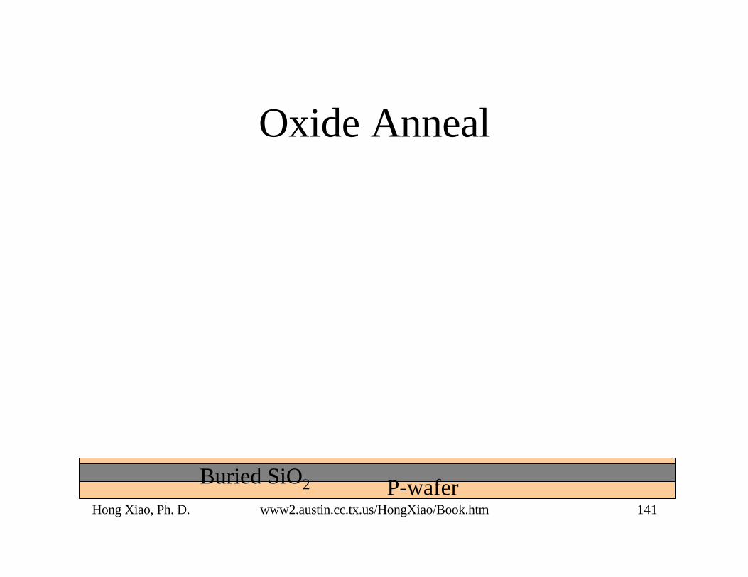
Oxide Anneal
P-waferBuried SiO2

Hong Xiao, Ph. D. www2.austin.cc.tx.us/HongXiao/Book.htm 142
Wafer Clean
P-waferBuried SiO2

Hong Xiao, Ph. D. www2.austin.cc.tx.us/HongXiao/Book.htm 143
Epitaxial Silicon Deposition
P-waferBuried SiO2
P-epi

Hong Xiao, Ph. D. www2.austin.cc.tx.us/HongXiao/Book.htm 144
Wafer Clean
P-waferBuried SiO2
P-epi
Hong Xiao, Ph. D. www2.austin.cc.tx.us/HongXiao/Book.htm 145
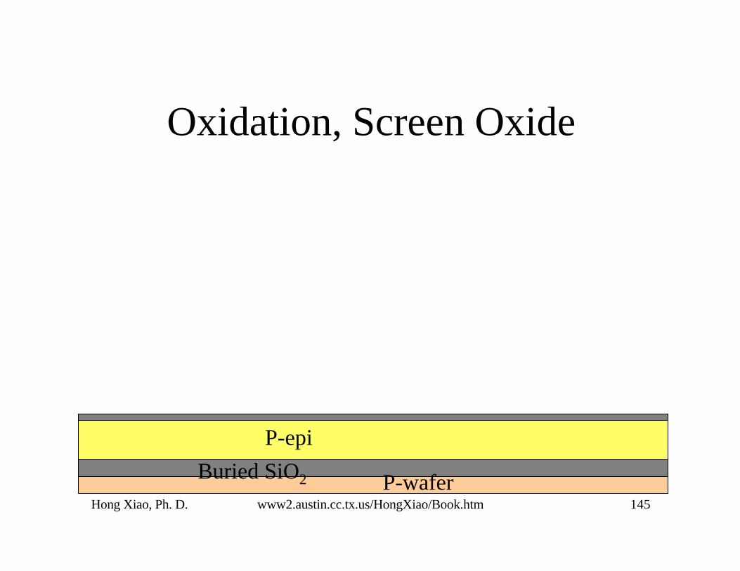
Oxidation, Screen Oxide
P-waferBuried SiO2
P-epi

Hong Xiao, Ph. D. www2.austin.cc.tx.us/HongXiao/Book.htm 146
Photoresist Coating and Baking
P-waferBuried SiO2
P-epi
Photoresist
Hong Xiao, Ph. D. www2.austin.cc.tx.us/HongXiao/Book.htm 147
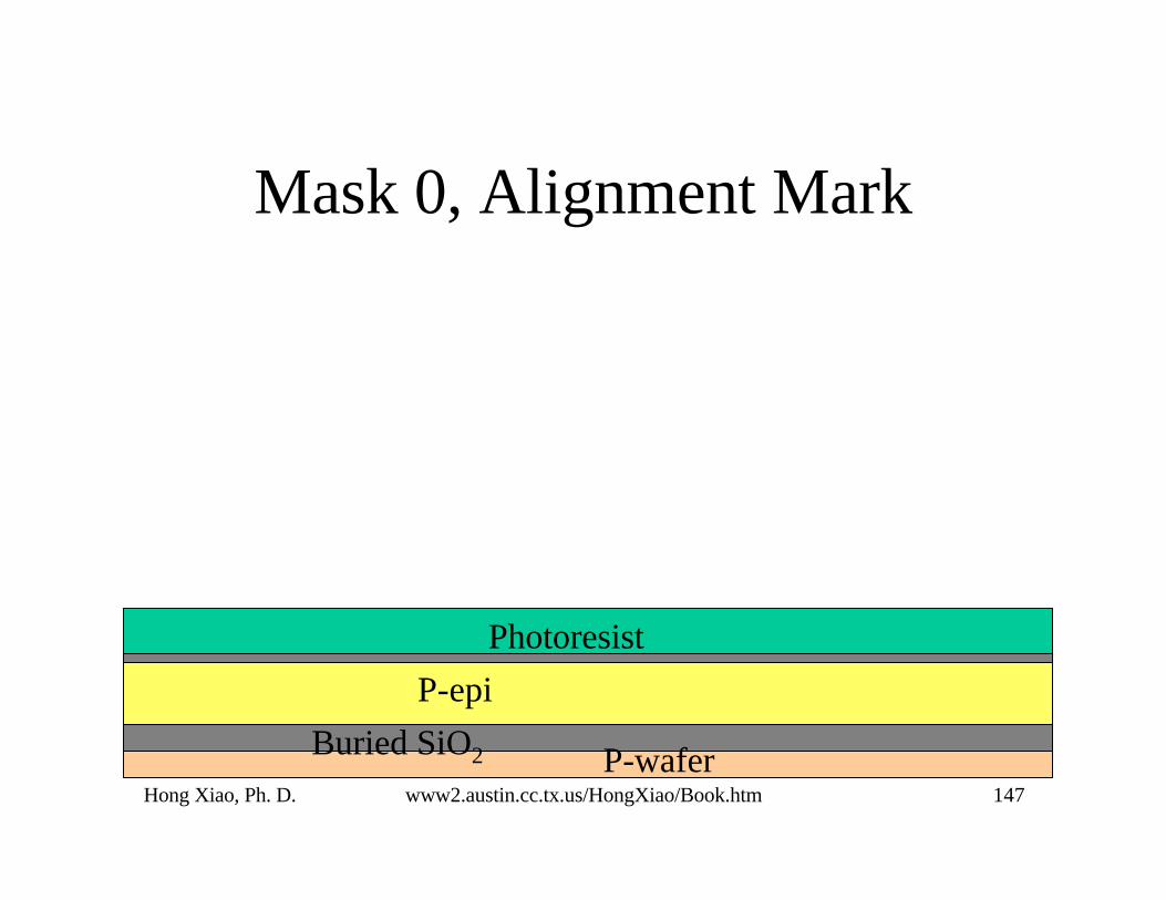
Mask 0, Alignment Mark
P-waferBuried SiO2
P-epi
Photoresist
Hong Xiao, Ph. D. www2.austin.cc.tx.us/HongXiao/Book.htm 148
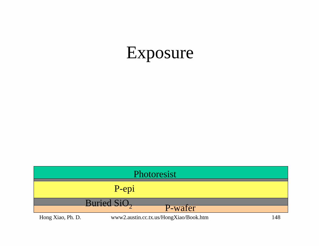
Exposure
P-waferBuried SiO2
P-epi
Photoresist
Hong Xiao, Ph. D. www2.austin.cc.tx.us/HongXiao/Book.htm 149
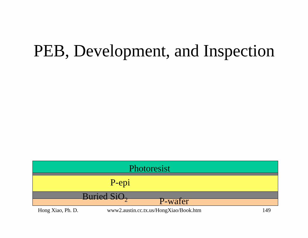
PEB, Development, and Inspection
P-waferBuried SiO2
P-epi
Photoresist
Hong Xiao, Ph. D. www2.austin.cc.tx.us/HongXiao/Book.htm 150
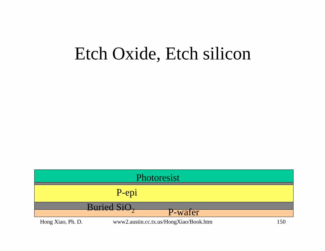
Etch Oxide, Etch silicon
P-waferBuried SiO2
P-epi
Photoresist
Hong Xiao, Ph. D. www2.austin.cc.tx.us/HongXiao/Book.htm 151
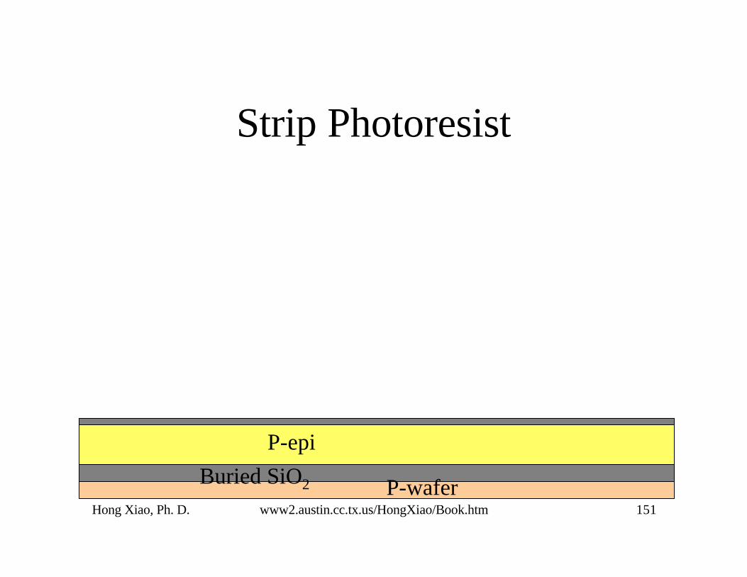
Strip Photoresist
P-waferBuried SiO2
P-epi
Hong Xiao, Ph. D. www2.austin.cc.tx.us/HongXiao/Book.htm 152
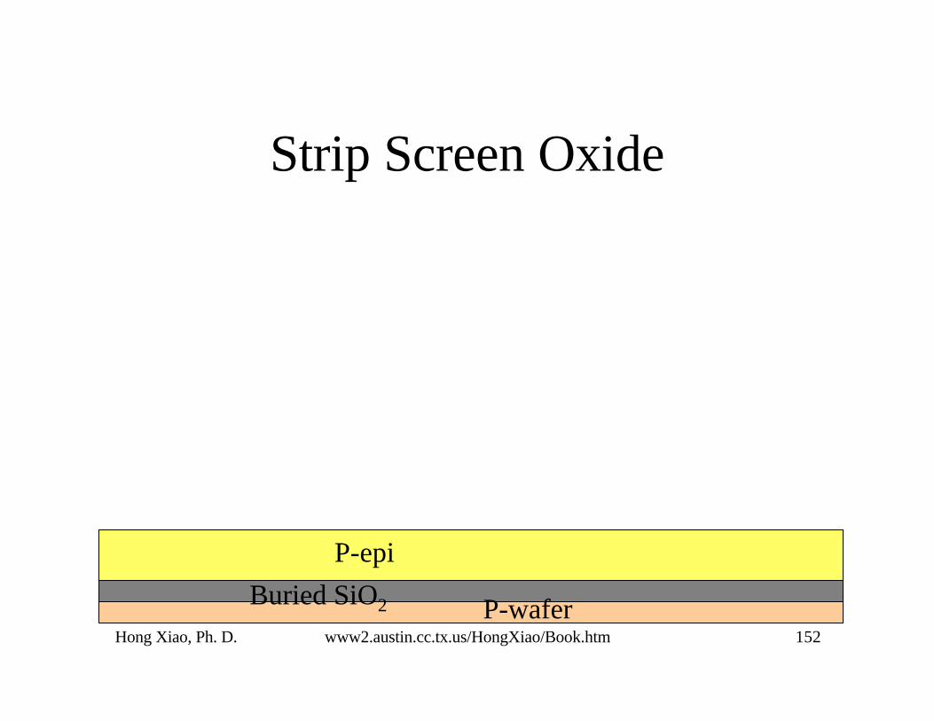
Strip Screen Oxide
P-waferBuried SiO2
P-epi

Hong Xiao, Ph. D. www2.austin.cc.tx.us/HongXiao/Book.htm 153
Wafer Clean
P-waferBuried SiO2
P-epi

Hong Xiao, Ph. D. www2.austin.cc.tx.us/HongXiao/Book.htm 154
Oxidation, Pad Oxide
P-waferBuried SiO2
P-epi

Hong Xiao, Ph. D. www2.austin.cc.tx.us/HongXiao/Book.htm 155
LPCVD Silicon Nitride
P-waferBuried SiO2
P-epi
Nitride

Hong Xiao, Ph. D. www2.austin.cc.tx.us/HongXiao/Book.htm 156
Photoresist Coating and Baking
P-waferBuried SiO2
P-epi
PhotoresistNitride
Hong Xiao, Ph. D. www2.austin.cc.tx.us/HongXiao/Book.htm 157
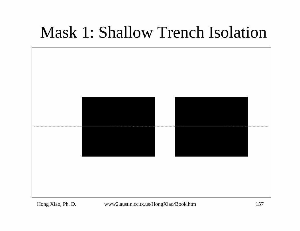
Mask 1: Shallow Trench Isolation

Hong Xiao, Ph. D. www2.austin.cc.tx.us/HongXiao/Book.htm 158
Alignment and Exposure
P-waferBuried SiO2
P-epi
PhotoresistNitride

Hong Xiao, Ph. D. www2.austin.cc.tx.us/HongXiao/Book.htm 159
PEB, Development, and Inspection
P-waferBuried SiO2
P-epi
PhotoresistNitride

Hong Xiao, Ph. D. www2.austin.cc.tx.us/HongXiao/Book.htm 160
Etch Nitride and Pad Oxide
P-waferBuried SiO2
P-epi
PhotoresistNitride

Hong Xiao, Ph. D. www2.austin.cc.tx.us/HongXiao/Book.htm 161
Strip Photoresist
P-waferBuried SiO2
P-epi
Nitride
Hong Xiao, Ph. D. www2.austin.cc.tx.us/HongXiao/Book.htm 162
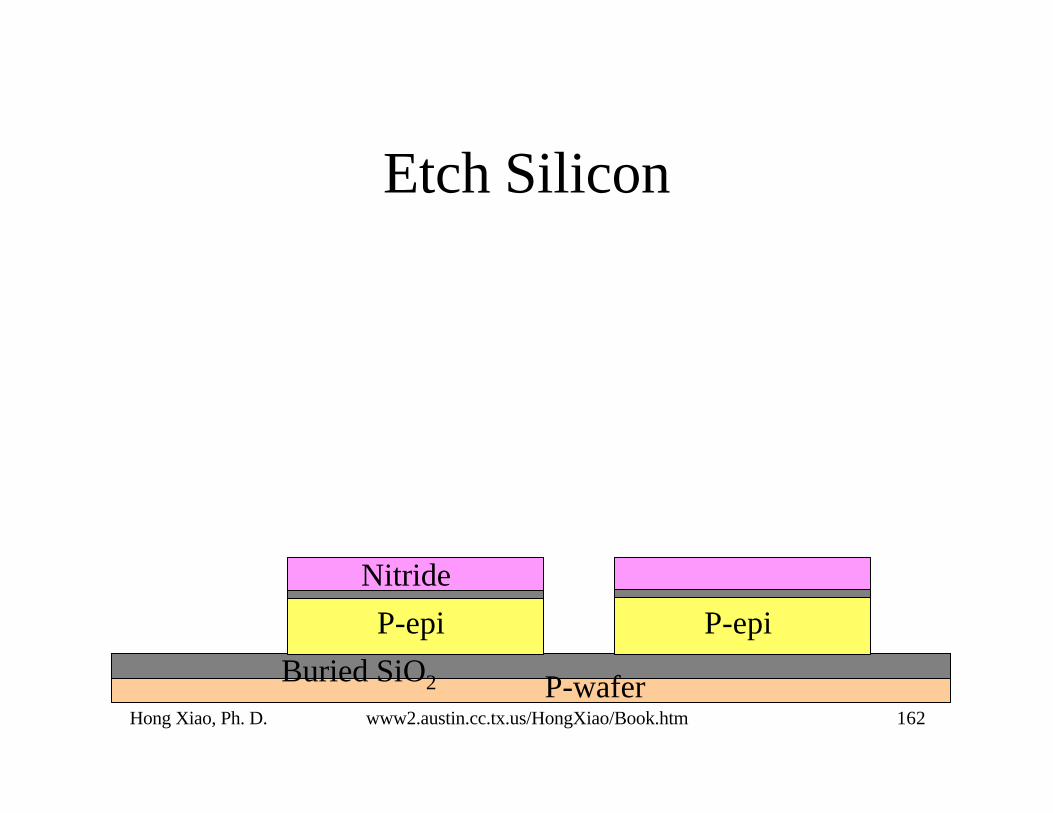
Etch Silicon
P-waferBuried SiO2
P-epi
Nitride
P-epi

Hong Xiao, Ph. D. www2.austin.cc.tx.us/HongXiao/Book.htm 163
Wafer Clean
P-waferBuried SiO2
P-epi
Nitride
P-epi

Hong Xiao, Ph. D. www2.austin.cc.tx.us/HongXiao/Book.htm 164
P-epi P-epi
Oxidation, Barrier Oxide
P-waferBuried SiO2
Nitride
Hong Xiao, Ph. D. www2.austin.cc.tx.us/HongXiao/Book.htm 165
P-epi P-epi
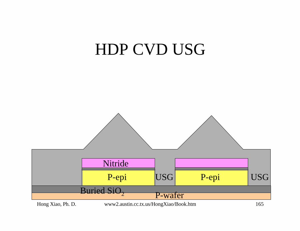
HDP CVD USG
P-waferBuried SiO2
Nitride
USGUSG
Hong Xiao, Ph. D. www2.austin.cc.tx.us/HongXiao/Book.htm 166
P-epi P-epi
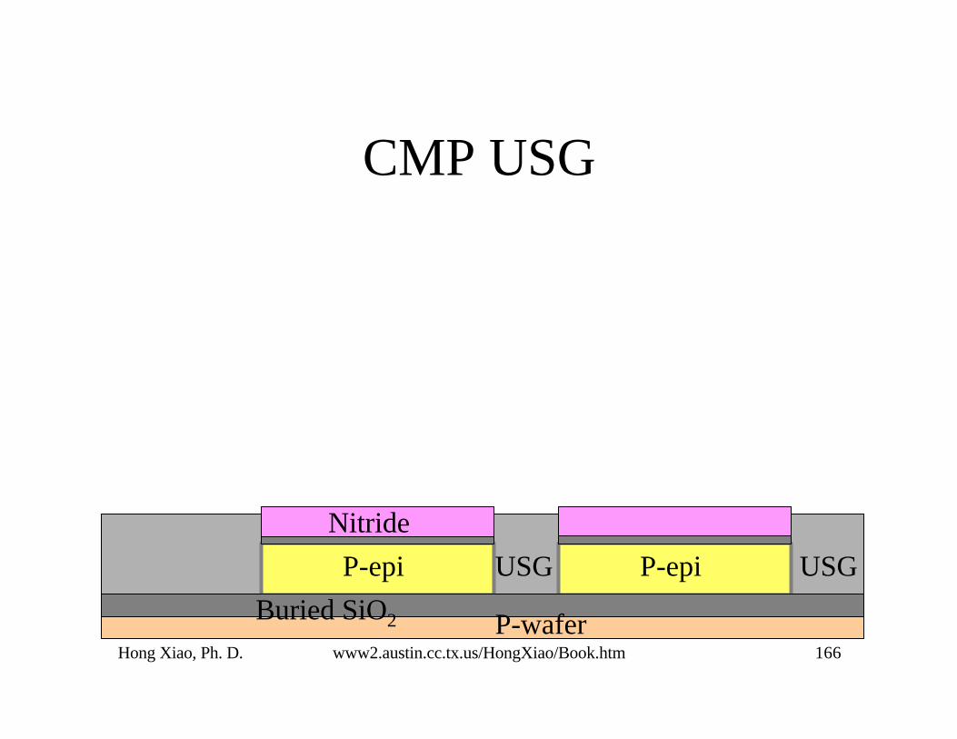
CMP USG
P-waferBuried SiO2
Nitride
USGUSG

Hong Xiao, Ph. D. www2.austin.cc.tx.us/HongXiao/Book.htm 167
P-epi P-epi
Strip Nitride
P-waferBuried SiO2
USGUSG

Hong Xiao, Ph. D. www2.austin.cc.tx.us/HongXiao/Book.htm 168
P-epi P-epi
Strip Pad Oxide
P-waferBuried SiO2
USGUSGSTI

Hong Xiao, Ph. D. www2.austin.cc.tx.us/HongXiao/Book.htm 169
P-epi P-epi
Wafer Clean
P-waferBuried SiO2
USGUSGSTI

Hong Xiao, Ph. D. www2.austin.cc.tx.us/HongXiao/Book.htm 170
P-epi P-epi
Oxidation, Sacrificial Oxide
P-waferBuried SiO2
USGUSGSTI
Hong Xiao, Ph. D. www2.austin.cc.tx.us/HongXiao/Book.htm 171
P-epi P-epi
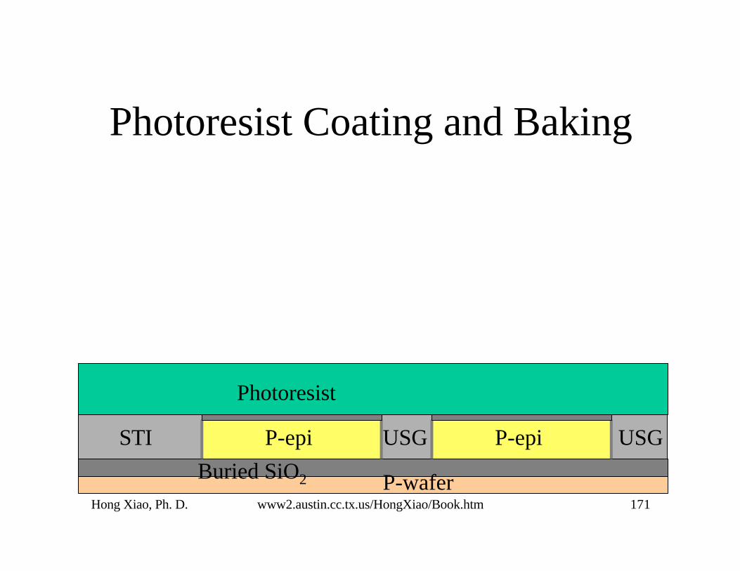
Photoresist Coating and Baking
P-waferBuried SiO2
USGUSGSTI
Photoresist

Hong Xiao, Ph. D. www2.austin.cc.tx.us/HongXiao/Book.htm 172
Mask 2: N-well

Hong Xiao, Ph. D. www2.austin.cc.tx.us/HongXiao/Book.htm 173
P-epi P-epi
Alignment and Exposure
P-waferBuried SiO2
USGUSGSTI
Photoresist

Hong Xiao, Ph. D. www2.austin.cc.tx.us/HongXiao/Book.htm 174
P-epi P-epi
PEB, Development, and Inspection
P-waferBuried SiO2
USGUSGSTI
Photoresist

Hong Xiao, Ph. D. www2.austin.cc.tx.us/HongXiao/Book.htm 175
P-epi
N-well Implantations
P-waferBuried SiO2
USGUSGSTI
Photoresist
N-well
Phosphorus ions, P+

Hong Xiao, Ph. D. www2.austin.cc.tx.us/HongXiao/Book.htm 176
P-epi
PMOS VT Adjust Implantation
P-waferBuried SiO2
USGUSGSTI
Photoresist
N-well
Boron ions, B+

Hong Xiao, Ph. D. www2.austin.cc.tx.us/HongXiao/Book.htm 177
P-epi
Strip Photoresist
P-waferBuried SiO2
USGUSGSTI N-well

Hong Xiao, Ph. D. www2.austin.cc.tx.us/HongXiao/Book.htm 178
P-epi
Photoresist Coating and Baking
P-waferBuried SiO2
USGUSGSTI N-well
Photoresist
Hong Xiao, Ph. D. www2.austin.cc.tx.us/HongXiao/Book.htm 179
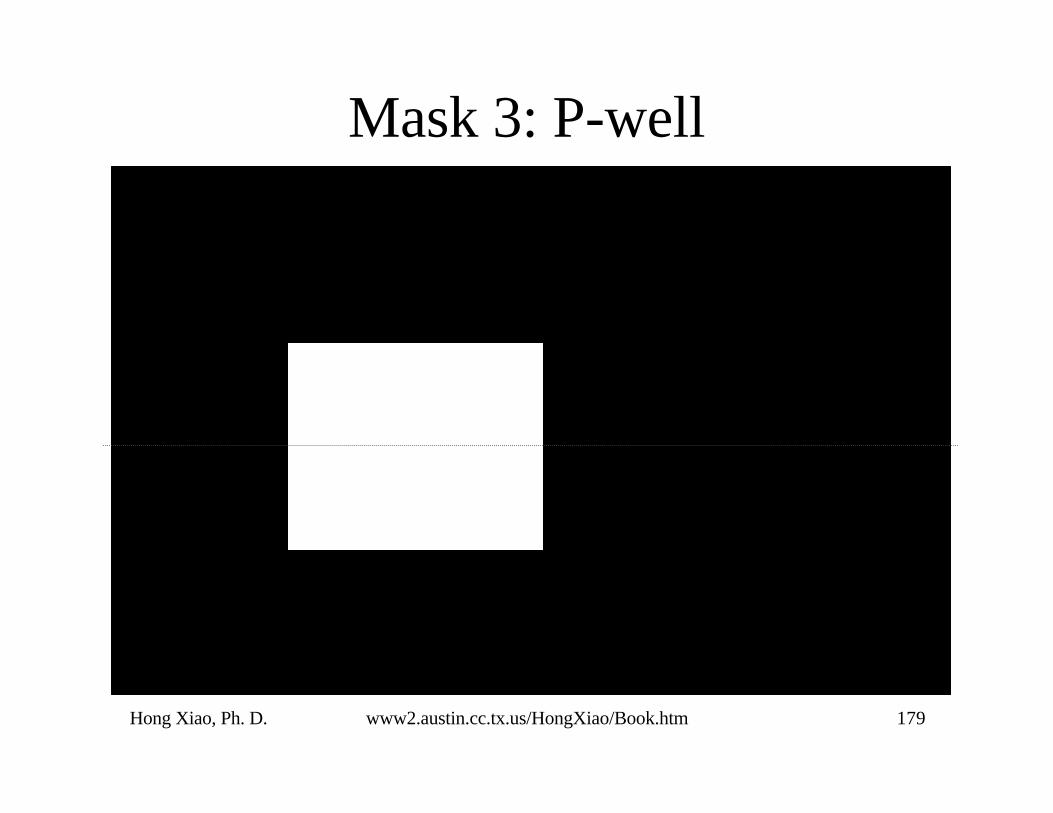
Mask 3: P-well
Hong Xiao, Ph. D. www2.austin.cc.tx.us/HongXiao/Book.htm 180
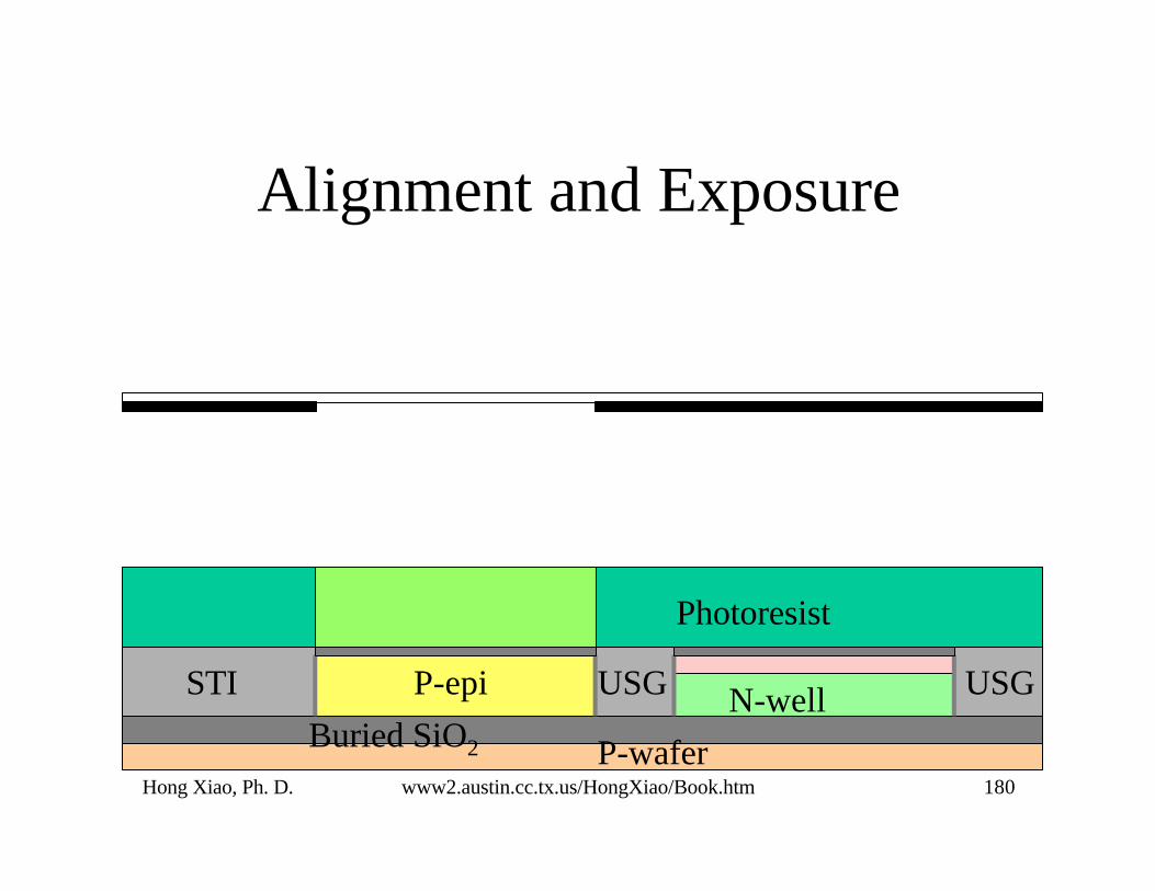
P-epi
Alignment and Exposure
P-waferBuried SiO2
USGUSGSTI N-well
Photoresist

Hong Xiao, Ph. D. www2.austin.cc.tx.us/HongXiao/Book.htm 181
P-epi
PEB, Development, and Inspection
P-waferBuried SiO2
USGUSGSTI N-well
Photoresist

Hong Xiao, Ph. D. www2.austin.cc.tx.us/HongXiao/Book.htm 182
P-well
P-well Implantations
P-waferBuried SiO2
USGUSGSTI N-well
Photoresist
Boron ions, B+

Hong Xiao, Ph. D. www2.austin.cc.tx.us/HongXiao/Book.htm 183
P-well
NMOS VT Adjust Implantation
P-waferBuried SiO2
USGUSGSTI N-well
Photoresist
Phosphorus ions, P+

Hong Xiao, Ph. D. www2.austin.cc.tx.us/HongXiao/Book.htm 184
P-well
Strip Photoresist
P-waferBuried SiO2
USGUSGSTI N-well
Hong Xiao, Ph. D. www2.austin.cc.tx.us/HongXiao/Book.htm 185
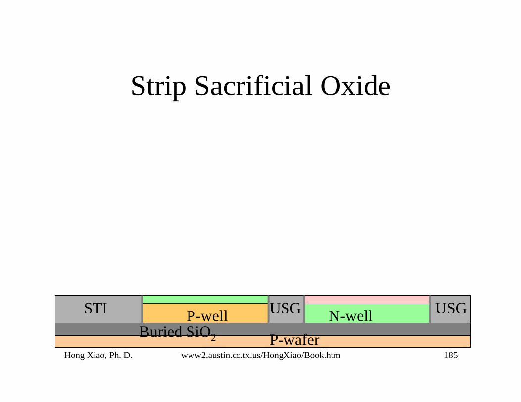
P-well
Strip Sacrificial Oxide
P-waferBuried SiO2
USGUSGSTI N-well

Hong Xiao, Ph. D. www2.austin.cc.tx.us/HongXiao/Book.htm 186
P-well
Wafer Clean
P-waferBuried SiO2
USGUSGSTI N-well
Hong Xiao, Ph. D. www2.austin.cc.tx.us/HongXiao/Book.htm 187
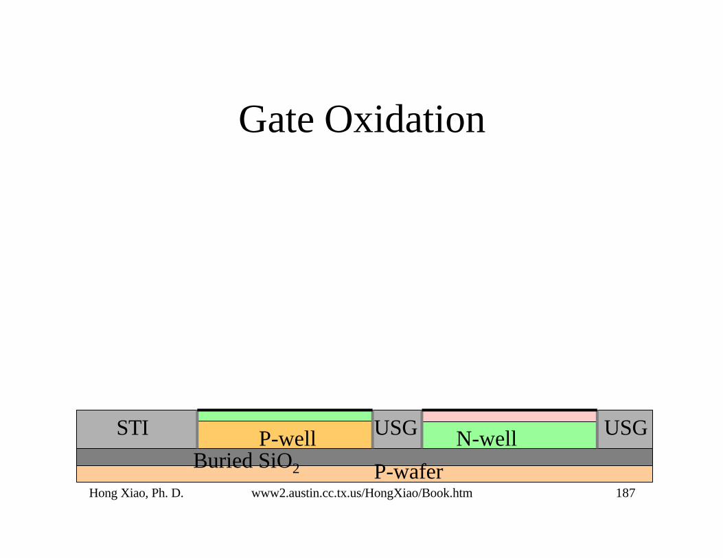
P-well
Gate Oxidation
P-waferBuried SiO2
USGUSGSTI N-well

Hong Xiao, Ph. D. www2.austin.cc.tx.us/HongXiao/Book.htm 188
P-well
LPCVD Amorphous Silicon
P-waferBuried SiO2
USGSTI N-well
α-Si
Gate oxide
USG
Hong Xiao, Ph. D. www2.austin.cc.tx.us/HongXiao/Book.htm 189
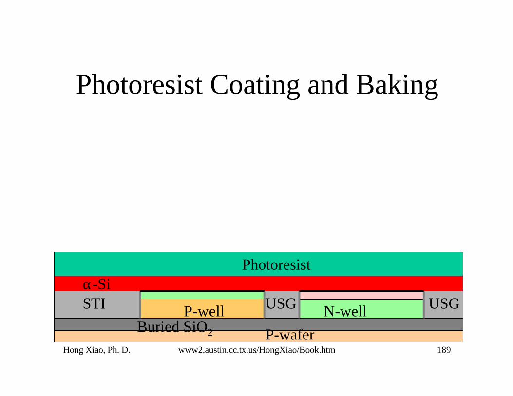
P-well
Photoresist Coating and Baking
P-waferBuried SiO2
USGUSGSTI N-well
α-SiPhotoresist

Hong Xiao, Ph. D. www2.austin.cc.tx.us/HongXiao/Book.htm 190
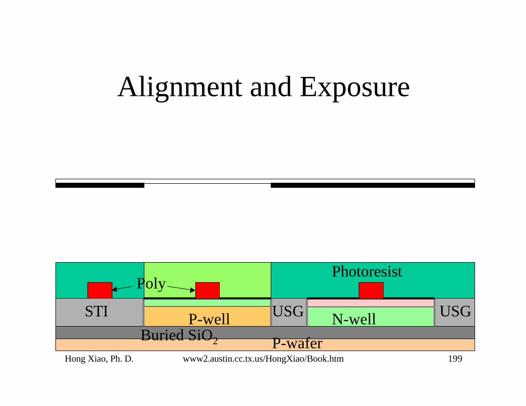
Mask 4, Gate and LocalInterconnection

Hong Xiao, Ph. D. www2.austin.cc.tx.us/HongXiao/Book.htm 191
P-well
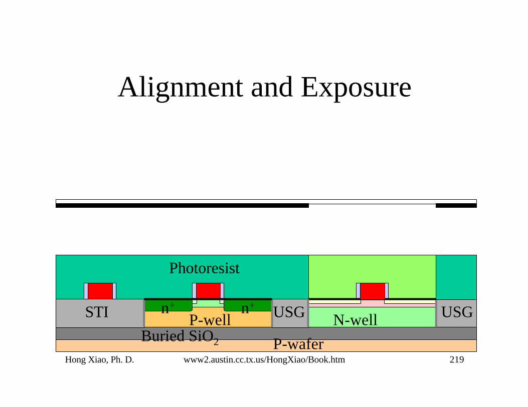
Alignment and Exposure
P-waferBuried SiO2
USGUSGSTI N-well
α-SiPhotoresist

Hong Xiao, Ph. D. www2.austin.cc.tx.us/HongXiao/Book.htm 192
P-well
PEB, Development, and Inspection
P-waferBuried SiO2
USGUSGSTI N-well
α-SiPhotoresist

Hong Xiao, Ph. D. www2.austin.cc.tx.us/HongXiao/Book.htm 193
P-well
Etch Amorphous Silicon
P-waferBuried SiO2
USGUSGSTI N-well
α-Si
PhotoresistGate oxide
Hong Xiao, Ph. D. www2.austin.cc.tx.us/HongXiao/Book.htm 194
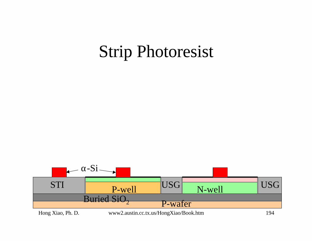
P-well
Strip Photoresist
P-waferBuried SiO2
USGUSGSTI N-well
α-Si

Hong Xiao, Ph. D. www2.austin.cc.tx.us/HongXiao/Book.htm 195
P-well
Wafer Clean
P-waferBuried SiO2
USGUSGSTI N-well
α-Si

Hong Xiao, Ph. D. www2.austin.cc.tx.us/HongXiao/Book.htm 196
P-well
Polysilicon Annealing and Oxidation
P-waferBuried SiO2
USGUSGSTI N-well
Poly Si

Hong Xiao, Ph. D. www2.austin.cc.tx.us/HongXiao/Book.htm 197
P-well
Photoresist Coating and Baking
P-waferBuried SiO2
USGUSGSTI N-well
PhotoresistPoly

Hong Xiao, Ph. D. www2.austin.cc.tx.us/HongXiao/Book.htm 198
Mask 5, NMOS LDD Implantation
Hong Xiao, Ph. D. www2.austin.cc.tx.us/HongXiao/Book.htm 199
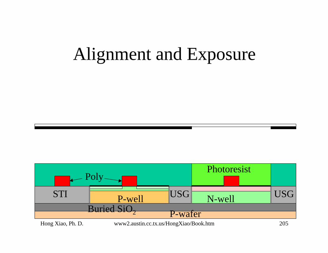
P-well
Alignment and Exposure
P-waferBuried SiO2
USGUSGSTI N-well
PolyPhotoresist

Hong Xiao, Ph. D. www2.austin.cc.tx.us/HongXiao/Book.htm 200
P-well
PEB, Development, and Inspection
P-waferBuried SiO2
USGUSGSTI N-well
Photoresist
Hong Xiao, Ph. D. www2.austin.cc.tx.us/HongXiao/Book.htm 201
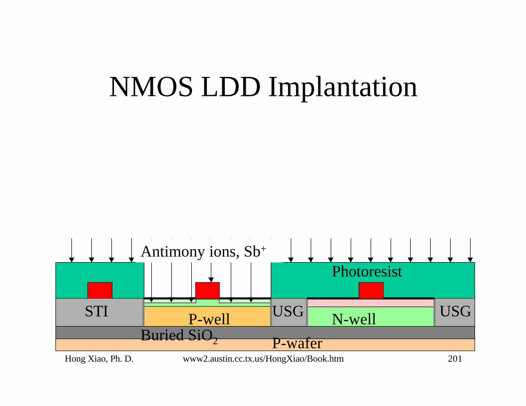
P-well
NMOS LDD Implantation
P-waferBuried SiO2
USGUSGSTI N-well
PhotoresistAntimony ions, Sb+

Hong Xiao, Ph. D. www2.austin.cc.tx.us/HongXiao/Book.htm 202
P-well
Strip Photoresist
P-waferBuried SiO2
USGUSGSTI N-well

Hong Xiao, Ph. D. www2.austin.cc.tx.us/HongXiao/Book.htm 203
P-well
Photoresist Coating and Baking
P-waferBuried SiO2
USGUSGSTI N-well
PolyPhotoresist

Hong Xiao, Ph. D. www2.austin.cc.tx.us/HongXiao/Book.htm 204
Mask 6: PMOS LDD Implantation
Hong Xiao, Ph. D. www2.austin.cc.tx.us/HongXiao/Book.htm 205
P-well
Alignment and Exposure
P-waferBuried SiO2
USGUSGSTI N-well
PolyPhotoresist

Hong Xiao, Ph. D. www2.austin.cc.tx.us/HongXiao/Book.htm 206
P-well
PEB, Development, and Inspection
P-waferBuried SiO2
USGUSGSTI N-well
PolyPhotoresist
Hong Xiao, Ph. D. www2.austin.cc.tx.us/HongXiao/Book.htm 207
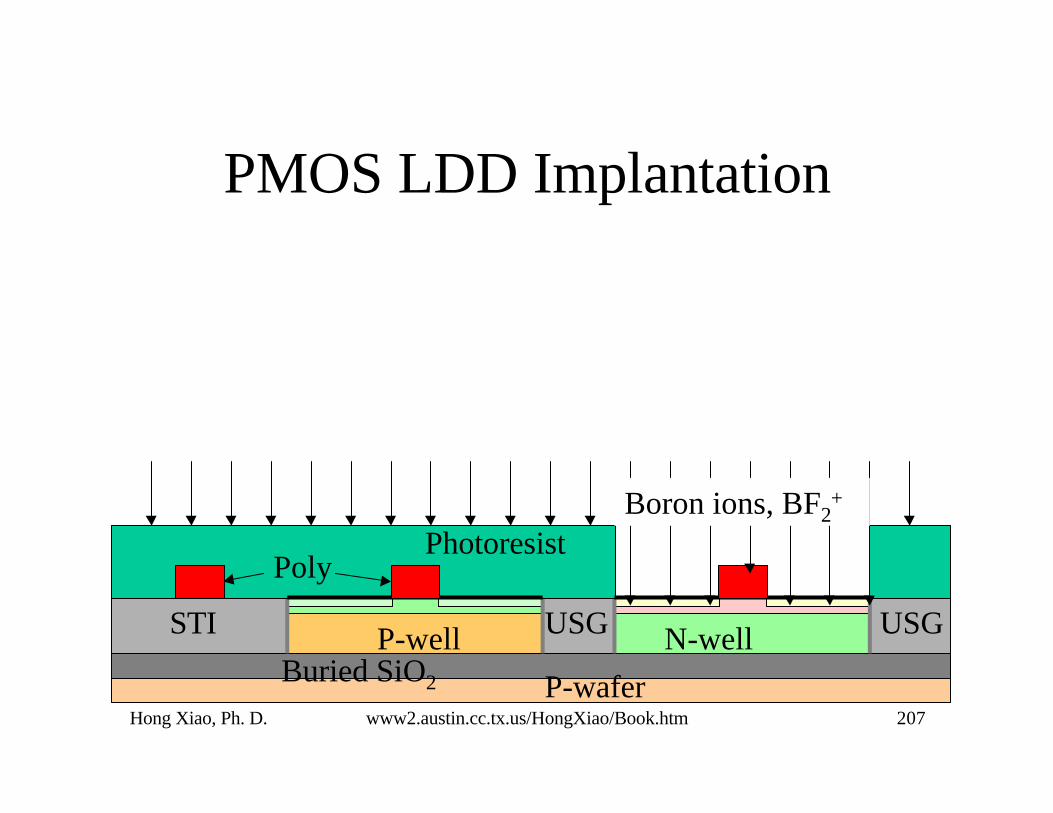
P-well
PMOS LDD Implantation
P-waferBuried SiO2
USGUSGSTI N-well
PolyPhotoresist
Boron ions, BF2+

Hong Xiao, Ph. D. www2.austin.cc.tx.us/HongXiao/Book.htm 208
P-well
Strip Photoresist
P-waferBuried SiO2
USGUSGSTI N-well

Hong Xiao, Ph. D. www2.austin.cc.tx.us/HongXiao/Book.htm 209
P-well
CVD USG, CVD Nitride
P-waferBuried SiO2
USGUSGSTI N-well

Hong Xiao, Ph. D. www2.austin.cc.tx.us/HongXiao/Book.htm 210
P-well
Nitride and USG Etchback
P-waferBuried SiO2
USGUSGSTI N-well
Sidewall spacersPolysilicon gate

Hong Xiao, Ph. D. www2.austin.cc.tx.us/HongXiao/Book.htm 211
P-well
Photoresist Coating and Baking
P-waferBuried SiO2
USGUSGSTI N-well
Photoresist

Hong Xiao, Ph. D. www2.austin.cc.tx.us/HongXiao/Book.htm 212
Mask 7, NMOS S/D Implantation

Hong Xiao, Ph. D. www2.austin.cc.tx.us/HongXiao/Book.htm 213
P-well
Alignment and Exposure
P-waferBuried SiO2
USGUSGSTI N-well
Photoresist

Hong Xiao, Ph. D. www2.austin.cc.tx.us/HongXiao/Book.htm 214
P-well
PEB, Development, and Inspection
P-waferBuried SiO2
USGUSGSTI N-well
Photoresist

Hong Xiao, Ph. D. www2.austin.cc.tx.us/HongXiao/Book.htm 215
P-well
NMOS S/D Implantation
P-waferBuried SiO2
USGN-well
Photoresist
STI USG
Arsenic ions, As+
Hong Xiao, Ph. D. www2.austin.cc.tx.us/HongXiao/Book.htm 216
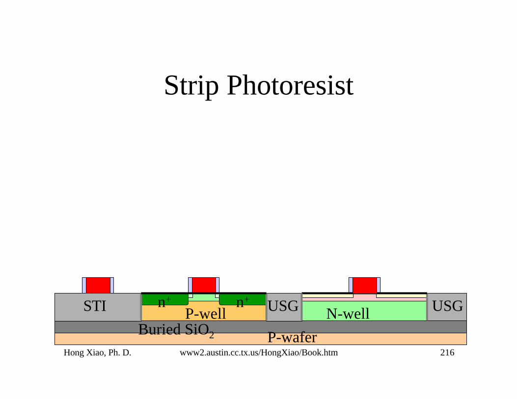
P-well
Strip Photoresist
P-waferBuried SiO2
USGN-wellSTI USGn+ n+

Hong Xiao, Ph. D. www2.austin.cc.tx.us/HongXiao/Book.htm 217
P-well
Photoresist Coating and Baking
P-waferBuried SiO2
USGN-wellSTI USGn+ n+
Photoresist

Hong Xiao, Ph. D. www2.austin.cc.tx.us/HongXiao/Book.htm 218
Mask 8, PMOS S/D Implantation
Hong Xiao, Ph. D. www2.austin.cc.tx.us/HongXiao/Book.htm 219
P-well
Alignment and Exposure
P-waferBuried SiO2
USGN-wellSTI USGn+ n+
Photoresist

Hong Xiao, Ph. D. www2.austin.cc.tx.us/HongXiao/Book.htm 220
P-well
PEB, Development, and Inspection
P-waferBuried SiO2
USGN-wellSTI USGn+ n+
Photoresist

Hong Xiao, Ph. D. www2.austin.cc.tx.us/HongXiao/Book.htm 221
P-well
PMOS S/D Implantation
P-waferBuried SiO2
USGN-wellSTI USGn+ n+
Photoresist
Boron ions, B+
Hong Xiao, Ph. D. www2.austin.cc.tx.us/HongXiao/Book.htm 222
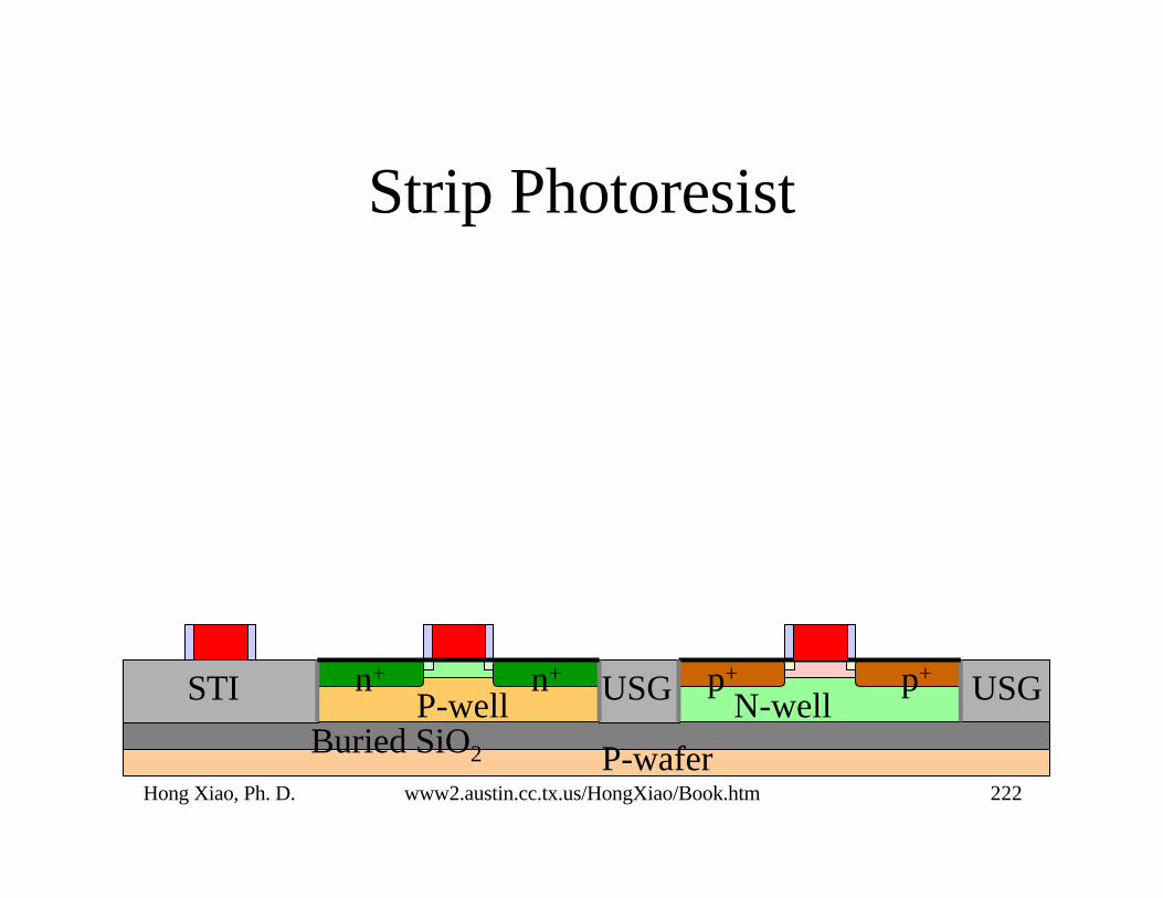
P-well
Strip Photoresist
P-waferBuried SiO2
USGN-wellSTI USGn+ n+ p+ p+

Hong Xiao, Ph. D. www2.austin.cc.tx.us/HongXiao/Book.htm 223
P-well
Rapid Thermal Annealing
P-waferBuried SiO2
USGN-wellSTI USGn+ n+ p+ p+
Hong Xiao, Ph. D. www2.austin.cc.tx.us/HongXiao/Book.htm 224
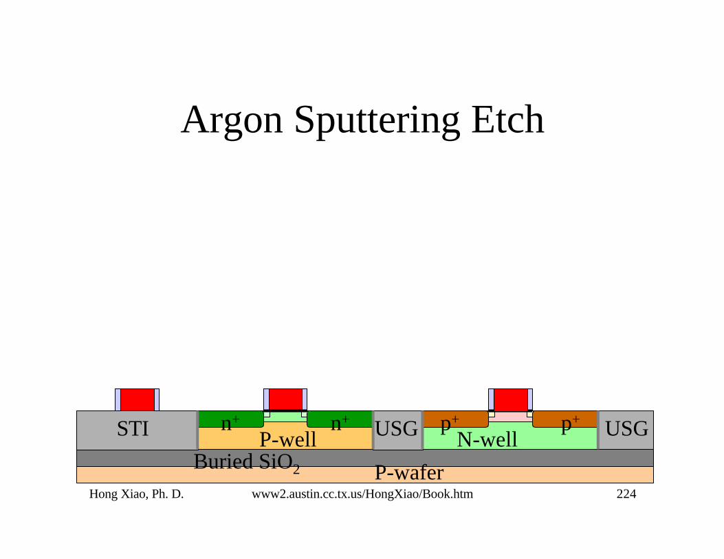
P-well
Argon Sputtering Etch
P-waferBuried SiO2
USGN-wellSTI USGn+ n+ p+ p+

Hong Xiao, Ph. D. www2.austin.cc.tx.us/HongXiao/Book.htm 225
P-well
Co and TiN Sputtering Deposition
P-waferBuried SiO2
USGN-wellSTI USGn+ n+ p+ p+
CoTiN
Hong Xiao, Ph. D. www2.austin.cc.tx.us/HongXiao/Book.htm 226
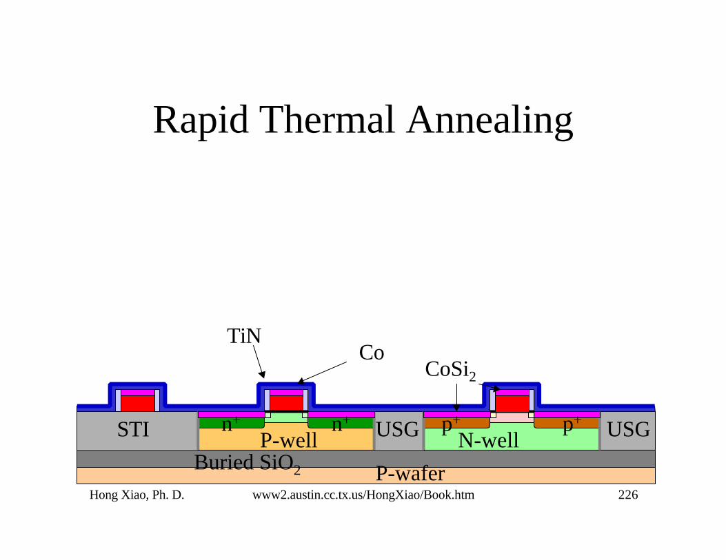
P-well
Rapid Thermal Annealing
P-waferBuried SiO2
USGN-wellSTI USGn+ n+ p+ p+
CoSi2
CoTiN

Hong Xiao, Ph. D. www2.austin.cc.tx.us/HongXiao/Book.htm 227
P-well
Strip Titanium Nitride and Cobalt
P-waferBuried SiO2
USGN-wellSTI USGn+ n+ p+ p+
CoSi2
Hong Xiao, Ph. D. www2.austin.cc.tx.us/HongXiao/Book.htm 228
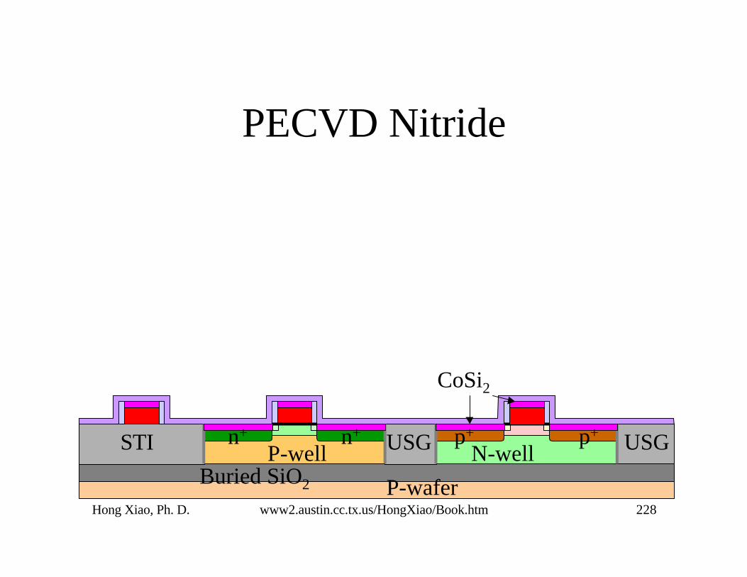
P-well
PECVD Nitride
P-waferBuried SiO2
USGN-wellSTI USGn+ n+ p+ p+
CoSi2

Hong Xiao, Ph. D. www2.austin.cc.tx.us/HongXiao/Book.htm 229
P-well
HDP CVD PSG
P-waferBuried SiO2
USGN-wellSTI USGn+ n+ p+ p+
PSG

Hong Xiao, Ph. D. www2.austin.cc.tx.us/HongXiao/Book.htm 230
P-well
CMP PSG
P-waferBuried SiO2
USGN-wellSTI USGn+ n+ p+ p+
PSG
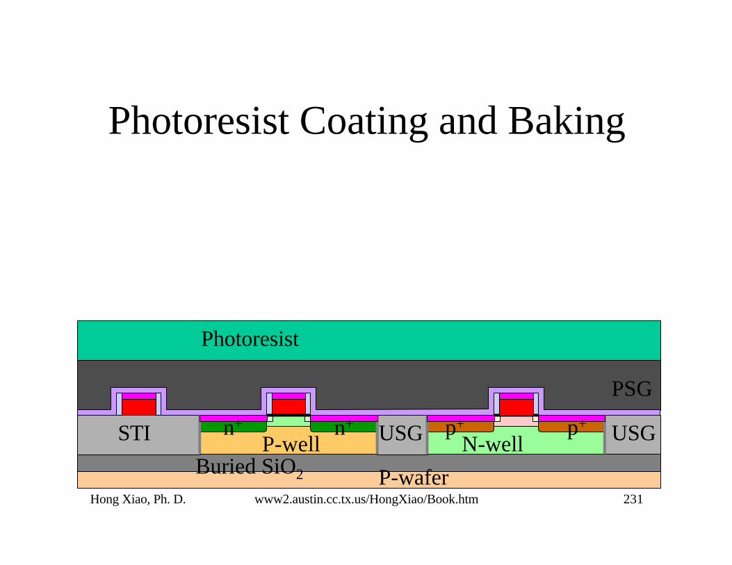
Hong Xiao, Ph. D. www2.austin.cc.tx.us/HongXiao/Book.htm 231
P-well
Photoresist Coating and Baking
P-waferBuried SiO2
USGN-wellSTI USGn+ n+ p+ p+
PSG
Photoresist

Hong Xiao, Ph. D. www2.austin.cc.tx.us/HongXiao/Book.htm 232
Mask 9, Contact and LocalInterconnection

Hong Xiao, Ph. D. www2.austin.cc.tx.us/HongXiao/Book.htm 233
P-well
Alignment and Exposure
P-waferBuried SiO2
USGN-wellSTI USGn+ n+ p+ p+
PSG
Photoresist
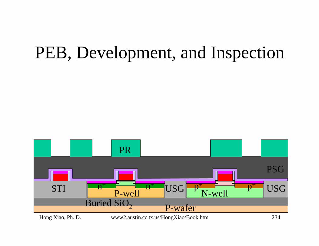
Hong Xiao, Ph. D. www2.austin.cc.tx.us/HongXiao/Book.htm 234
P-well
PEB, Development, and Inspection
P-waferBuried SiO2
USGN-wellSTI USGn+ n+ p+ p+
PSG
PR

Hong Xiao, Ph. D. www2.austin.cc.tx.us/HongXiao/Book.htm 235
P-well
Etch PSG
P-waferBuried SiO2
USGN-wellSTI USGn+ n+ p+ p+
PSG
PR

Hong Xiao, Ph. D. www2.austin.cc.tx.us/HongXiao/Book.htm 236
P-well
Strip Photoresist
P-waferBuried SiO2
USGN-wellSTI USGn+ n+ p+ p+
PSG

Hong Xiao, Ph. D. www2.austin.cc.tx.us/HongXiao/Book.htm 237
P-well
Argon Sputtering Etch
P-waferBuried SiO2
USGN-wellSTI USGn+ n+ p+ p+
PSG

Hong Xiao, Ph. D. www2.austin.cc.tx.us/HongXiao/Book.htm 238
P-well
Ti and TiN Sputtering Deposition
P-waferBuried SiO2
USGN-wellSTI USGn+ n+ p+ p+
PSG
Ti/TiN glue and barrier layers

Hong Xiao, Ph. D. www2.austin.cc.tx.us/HongXiao/Book.htm 239
P-well
Tungsten CVD
P-waferBuried SiO2
USGN-wellSTI USGn+ n+ p+ p+
PSG
Ti/TiN glue and barrier layers
TungstenW
Hong Xiao, Ph. D. www2.austin.cc.tx.us/HongXiao/Book.htm 240
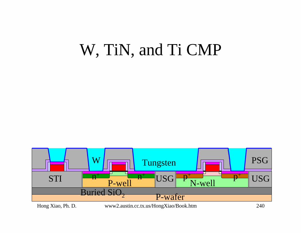
P-well
W, TiN, and Ti CMP
P-waferBuried SiO2
USGN-wellSTI USGn+ n+ p+ p+
PSGW Tungsten

Hong Xiao, Ph. D. www2.austin.cc.tx.us/HongXiao/Book.htm 241
PECVD Silicon Carbide Seal Layer
P-well
P-waferBuried SiO2
USGN-wellSTI USGn+ n+ p+ p+
PSGW Tungsten
Hong Xiao, Ph. D. www2.austin.cc.tx.us/HongXiao/Book.htm 242
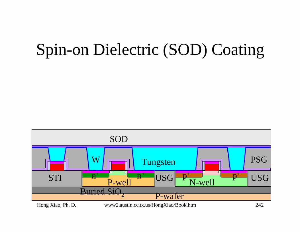
Spin-on Dielectric (SOD) Coating
SOD
P-well
P-waferBuried SiO2
USGN-wellSTI USGn+ n+ p+ p+
PSGW Tungsten

Hong Xiao, Ph. D. www2.austin.cc.tx.us/HongXiao/Book.htm 243
SOD Cure
SOD
P-well
P-waferBuried SiO2
USGN-wellSTI USGn+ n+ p+ p+
PSGW Tungsten
Hong Xiao, Ph. D. www2.austin.cc.tx.us/HongXiao/Book.htm 244
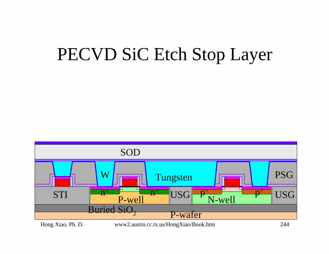
PECVD SiC Etch Stop Layer
SOD
P-well
P-waferBuried SiO2
USGN-wellSTI USGn+ n+ p+ p+
PSGW Tungsten

Hong Xiao, Ph. D. www2.austin.cc.tx.us/HongXiao/Book.htm 245
SOD Coating and Curing
SOD
SOD
P-well
P-waferBuried SiO2
USGN-wellSTI USGn+ n+ p+ p+
PSGW Tungsten

Hong Xiao, Ph. D. www2.austin.cc.tx.us/HongXiao/Book.htm 246
PE-TEOS Cap
SOD
SOD
P-well
P-waferBuried SiO2
USGN-wellSTI USGn+ n+ p+ p+
PSGW Tungsten

Hong Xiao, Ph. D. www2.austin.cc.tx.us/HongXiao/Book.htm 247
Photoresist Coating and Baking
SOD
SOD
Photoresist
P-well
P-waferBuried SiO2
USGN-wellSTI USGn+ n+ p+ p+
PSGW Tungsten

Hong Xiao, Ph. D. www2.austin.cc.tx.us/HongXiao/Book.htm 248
Mask 10, Via 1
Hong Xiao, Ph. D. www2.austin.cc.tx.us/HongXiao/Book.htm 249
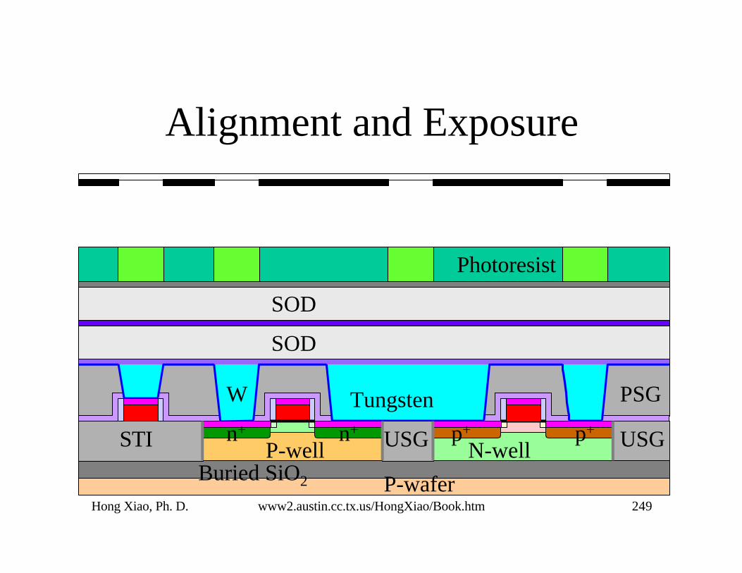
Alignment and Exposure
SOD
SOD
Photoresist
P-well
P-waferBuried SiO2
USGN-wellSTI USGn+ n+ p+ p+
PSGW Tungsten

Hong Xiao, Ph. D. www2.austin.cc.tx.us/HongXiao/Book.htm 250
PEB, Development, and Inspection
SOD
SOD
Photoresist
P-well
P-waferBuried SiO2
USGN-wellSTI USGn+ n+ p+ p+
PSGW Tungsten

Hong Xiao, Ph. D. www2.austin.cc.tx.us/HongXiao/Book.htm 251
Etch PE-TEOS&SOD, Stop on SiC
SOD
SOD
Photoresist
P-well
P-waferBuried SiO2
USGN-wellSTI USGn+ n+ p+ p+
PSGW Tungsten

Hong Xiao, Ph. D. www2.austin.cc.tx.us/HongXiao/Book.htm 252
Strip Photoresist
SOD
SOD
P-well
P-waferBuried SiO2
USGN-wellSTI USGn+ n+ p+ p+
PSGW Tungsten
Hong Xiao, Ph. D. www2.austin.cc.tx.us/HongXiao/Book.htm 253
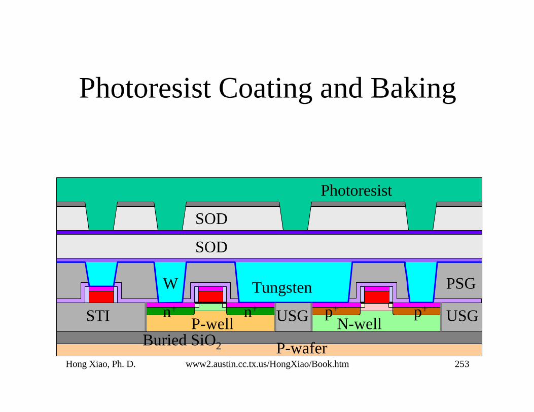
Photoresist Coating and Baking
SOD
SOD
Photoresist
P-well
P-waferBuried SiO2
USGN-wellSTI USGn+ n+ p+ p+
PSGW Tungsten
Hong Xiao, Ph. D. www2.austin.cc.tx.us/HongXiao/Book.htm 254
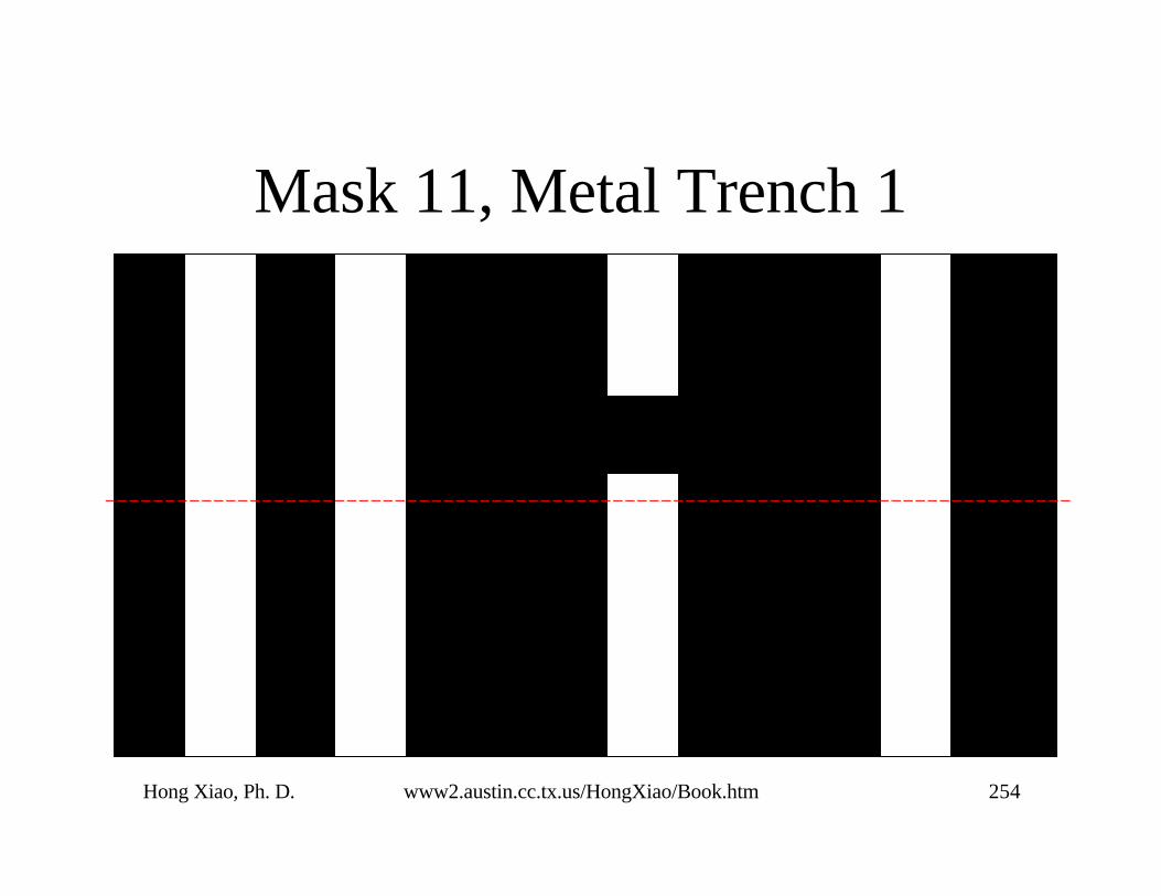
Mask 11, Metal Trench 1

Hong Xiao, Ph. D. www2.austin.cc.tx.us/HongXiao/Book.htm 255
Alignment and Exposure
SOD
SOD
Photoresist
P-well
P-waferBuried SiO2
USGN-wellSTI USGn+ n+ p+ p+
PSGW Tungsten

Hong Xiao, Ph. D. www2.austin.cc.tx.us/HongXiao/Book.htm 256
PEB, Development, and Inspection
SOD
SOD
Photoresist
P-well
P-waferBuried SiO2
USGN-wellSTI USGn+ n+ p+ p+
PSGW Tungsten

Hong Xiao, Ph. D. www2.austin.cc.tx.us/HongXiao/Book.htm 257
Etch Trench
P-well
P-waferBuried SiO2
USGN-wellSTI USGn+ n+ p+ p+
PSGW Tungsten
SOD
SOD
Photoresist

Hong Xiao, Ph. D. www2.austin.cc.tx.us/HongXiao/Book.htm 258
Strip Photoresist
SOD
P-well
P-waferBuried SiO2
USGN-wellSTI USGn+ n+ p+ p+
PSGW Tungsten
SOD

Hong Xiao, Ph. D. www2.austin.cc.tx.us/HongXiao/Book.htm 259
Argon Sputtering Clean
SOD
P-well
P-waferBuried SiO2
USGN-wellSTI USGn+ n+ p+ p+
PSGW Tungsten
SOD

Hong Xiao, Ph. D. www2.austin.cc.tx.us/HongXiao/Book.htm 260
Ta and TaN Barrier Layer PVD
SOD
P-well
P-waferBuried SiO2
USGN-wellSTI USGn+ n+ p+ p+
PSGW Tungsten
SOD

Hong Xiao, Ph. D. www2.austin.cc.tx.us/HongXiao/Book.htm 261
P-well
P-waferBuried SiO2
USGN-wellSTI USGn+ n+ p+ p+
PSGW Tungsten
Cu Seed Layer PVD
SOD
SOD

Hong Xiao, Ph. D. www2.austin.cc.tx.us/HongXiao/Book.htm 262
Bulk Copper Electrochemical Plating
P-well
P-waferBuried SiO2
USGN-wellSTI USGn+ n+ p+ p+
PSGW Tungsten
SOD
SODCu 1 Cu 1 Cu 1 Cu 1
Hong Xiao, Ph. D. www2.austin.cc.tx.us/HongXiao/Book.htm 263
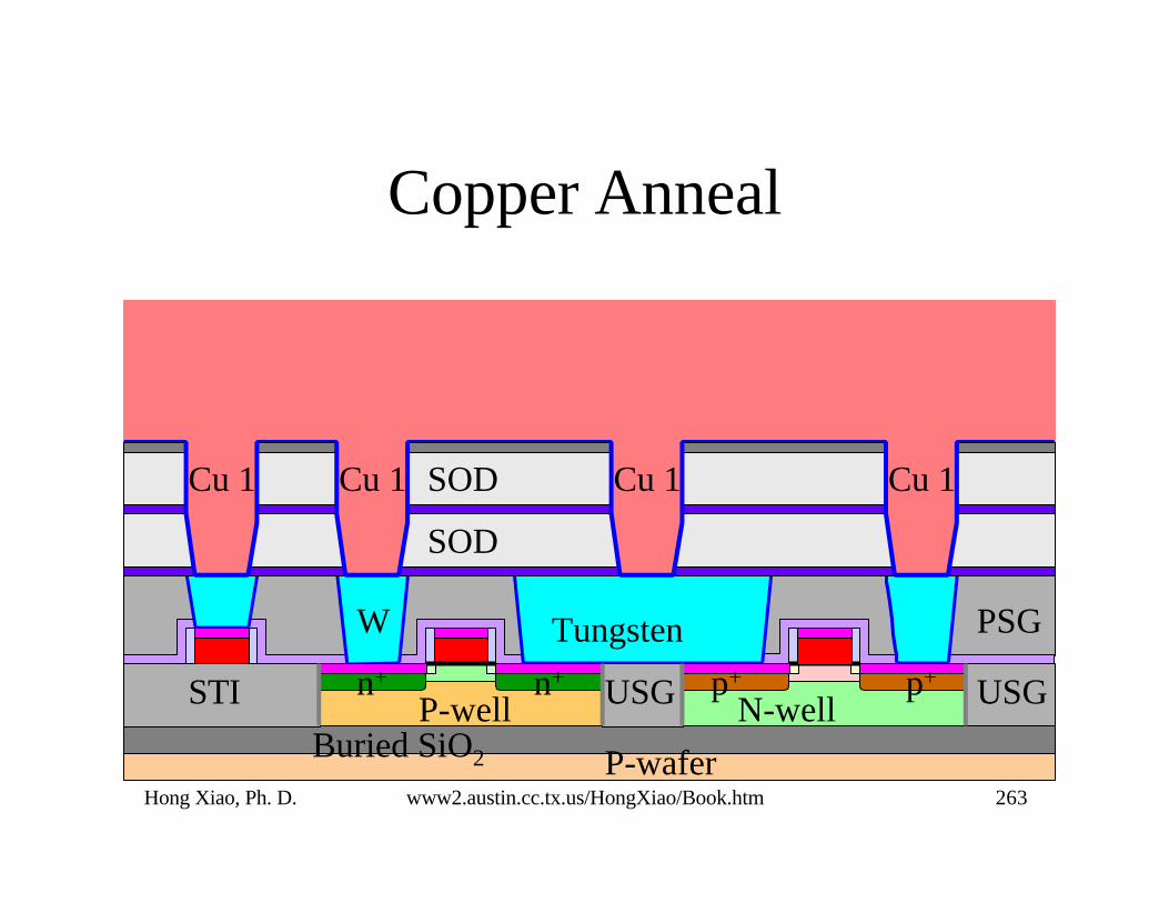
Copper Anneal
P-well
P-waferBuried SiO2
USGN-wellSTI USGn+ n+ p+ p+
PSGW Tungsten
SOD
SODCu 1 Cu 1 Cu 1 Cu 1

Hong Xiao, Ph. D. www2.austin.cc.tx.us/HongXiao/Book.htm 264
Cu, Ta, and TaN CMP
P-well
P-waferBuried SiO2
USGN-wellSTI USGn+ n+ p+ p+
PSGW Tungsten
SOD
SODCu 1 Cu 1 Cu 1 Cu 1

Hong Xiao, Ph. D. www2.austin.cc.tx.us/HongXiao/Book.htm 265
P-well
P-waferBuried SiO2
USGN-wellSTI USGn+ n+ p+ p+
PSGW Tungsten
SOD
SODCu 1 Cu 1 Cu 1 Cu 1
PECVD SiC Seal Layer

Hong Xiao, Ph. D. www2.austin.cc.tx.us/HongXiao/Book.htm 266
P-well
P-waferBuried SiO2
USGN-wellSTI USGn+ n+ p+ p+
PSGW Tungsten
SOD
SODCu 1 Cu 1 Cu 1 Cu 1
Spin-on Dielectric (SOD) Coating
SOD

Hong Xiao, Ph. D. www2.austin.cc.tx.us/HongXiao/Book.htm 267
P-well
P-waferBuried SiO2
USGN-wellSTI USGn+ n+ p+ p+
PSGW Tungsten
SOD
SODCu 1 Cu 1 Cu 1 Cu 1
SOD Curing
SOD
Hong Xiao, Ph. D. www2.austin.cc.tx.us/HongXiao/Book.htm 268
P-well
P-waferBuried SiO2
USGN-wellSTI USGn+ n+ p+ p+
PSGW Tungsten
SOD
SODCu 1 Cu 1 Cu 1 Cu 1
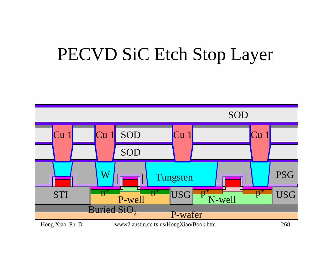
PECVD SiC Etch Stop Layer
SOD

Hong Xiao, Ph. D. www2.austin.cc.tx.us/HongXiao/Book.htm 269
P-well
P-waferBuried SiO2
USGN-wellSTI USGn+ n+ p+ p+
PSGW Tungsten
SOD
SODCu 1 Cu 1 Cu 1 Cu 1
SOD Coating and Curing
SOD
SOD

Hong Xiao, Ph. D. www2.austin.cc.tx.us/HongXiao/Book.htm 270
P-well
P-waferBuried SiO2
USGN-wellSTI USGn+ n+ p+ p+
PSGW Tungsten
SOD
SODCu 1 Cu 1 Cu 1 Cu 1
PE-TEOS Cap
SOD
SOD
Hong Xiao, Ph. D. www2.austin.cc.tx.us/HongXiao/Book.htm 271
P-well
P-waferBuried SiO2
USGN-wellSTI USGn+ n+ p+ p+
PSGW Tungsten
SOD
SODCu 1 Cu 1 Cu 1 Cu 1
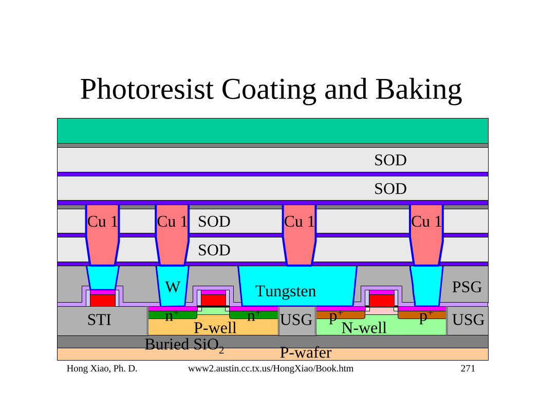
Photoresist Coating and Baking
SOD
SOD

Hong Xiao, Ph. D. www2.austin.cc.tx.us/HongXiao/Book.htm 272
Mask 12, Metal Trench 2

Hong Xiao, Ph. D. www2.austin.cc.tx.us/HongXiao/Book.htm 273
P-well
P-waferBuried SiO2
USGN-wellSTI USGn+ n+ p+ p+
PSGW Tungsten
SOD
SODCu 1 Cu 1 Cu 1 Cu 1
Alignment and Exposure
SOD
SOD
Hong Xiao, Ph. D. www2.austin.cc.tx.us/HongXiao/Book.htm 274
P-well
P-waferBuried SiO2
USGN-wellSTI USGn+ n+ p+ p+
PSGW Tungsten
SOD
SODCu 1 Cu 1 Cu 1 Cu 1
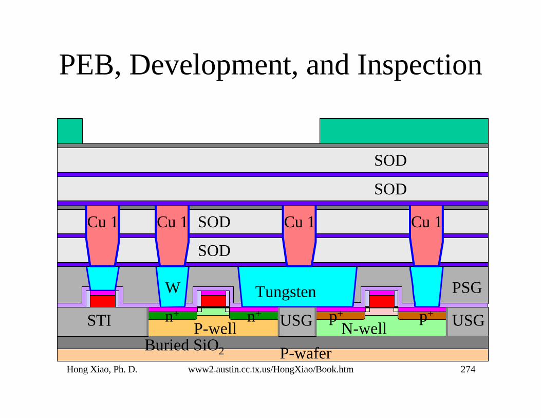
PEB, Development, and Inspection
SOD
SOD

Hong Xiao, Ph. D. www2.austin.cc.tx.us/HongXiao/Book.htm 275
P-well
P-waferBuried SiO2
USGN-wellSTI USGn+ n+ p+ p+
PSGW Tungsten
SOD
SODCu 1 Cu 1 Cu 1 Cu 1
Etch Trench, Stop on SiC Layer
SOD
SODSiCPhotoresist

Hong Xiao, Ph. D. www2.austin.cc.tx.us/HongXiao/Book.htm 276
P-well
P-waferBuried SiO2
USGN-wellSTI USGn+ n+ p+ p+
PSGW Tungsten
SOD
SODCu 1 Cu 1 Cu 1 Cu 1
Strip Photoresist
SOD
SODSiC
Hong Xiao, Ph. D. www2.austin.cc.tx.us/HongXiao/Book.htm 277
P-well
P-waferBuried SiO2
USGN-wellSTI USGn+ n+ p+ p+
PSGW Tungsten
SOD
SODCu 1 Cu 1 Cu 1 Cu 1
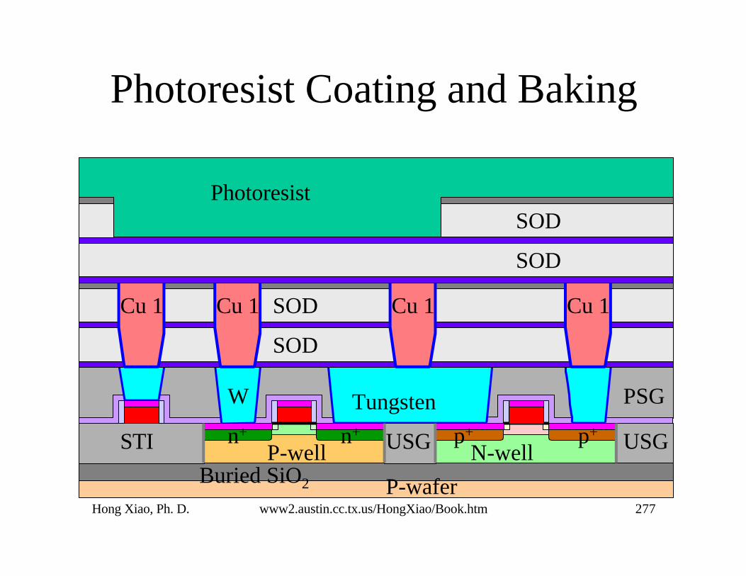
Photoresist Coating and Baking
SOD
SODPhotoresist

Hong Xiao, Ph. D. www2.austin.cc.tx.us/HongXiao/Book.htm 278
Mask 13, Via 2

Hong Xiao, Ph. D. www2.austin.cc.tx.us/HongXiao/Book.htm 279
P-well
P-waferBuried SiO2
USGN-wellSTI USGn+ n+ p+ p+
PSGW Tungsten
SOD
SODCu 1 Cu 1 Cu 1 Cu 1
Alignment and Exposure
SOD
SODPhotoresist
Hong Xiao, Ph. D. www2.austin.cc.tx.us/HongXiao/Book.htm 280
P-well
P-waferBuried SiO2
USGN-wellSTI USGn+ n+ p+ p+
PSGW Tungsten
SOD
SODCu 1 Cu 1 Cu 1 Cu 1
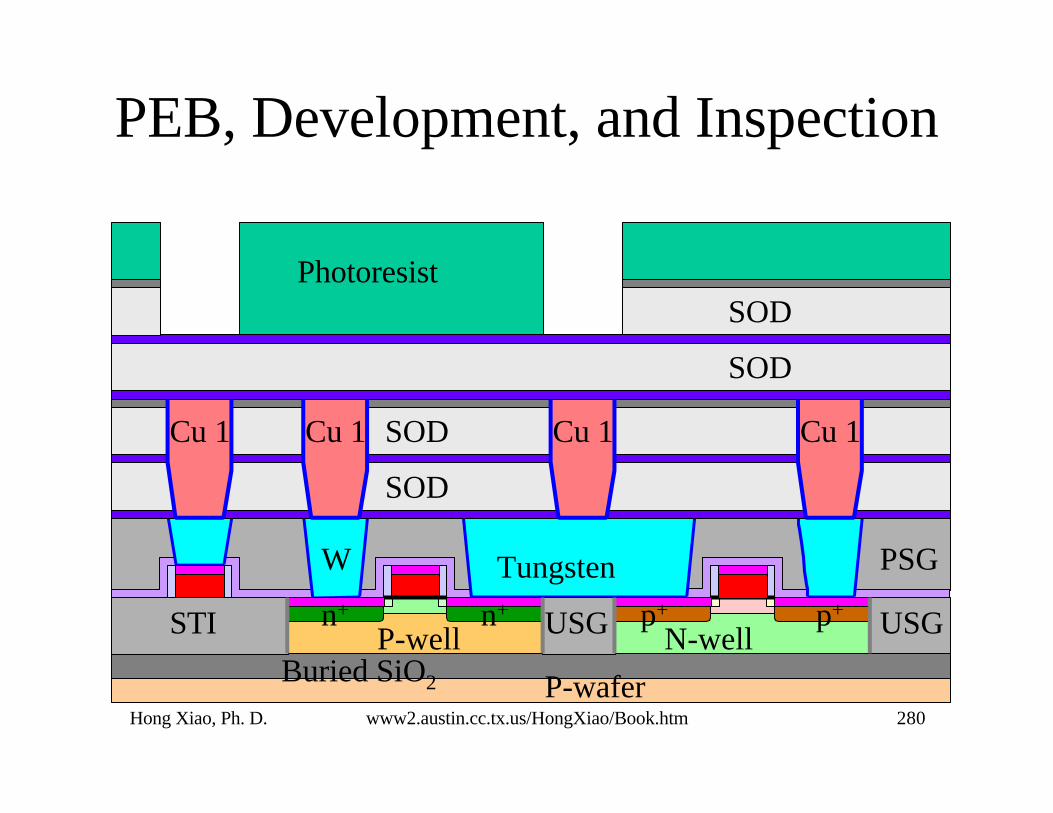
PEB, Development, and Inspection
SOD
SODPhotoresist

Hong Xiao, Ph. D. www2.austin.cc.tx.us/HongXiao/Book.htm 281
P-well
P-waferBuried SiO2
USGN-wellSTI USGn+ n+ p+ p+
PSGW Tungsten
SOD
SODCu 1 Cu 1 Cu 1 Cu 1
Via2 Etch
SOD
SODPhotoresist

Hong Xiao, Ph. D. www2.austin.cc.tx.us/HongXiao/Book.htm 282
P-well
P-waferBuried SiO2
USGN-wellSTI USGn+ n+ p+ p+
PSGW Tungsten
SOD
SODCu 1 Cu 1 Cu 1 Cu 1
Strip Photoresist
SOD
SOD

Hong Xiao, Ph. D. www2.austin.cc.tx.us/HongXiao/Book.htm 283
P-well
P-waferBuried SiO2
USGN-wellSTI USGn+ n+ p+ p+
PSGW Tungsten
SOD
SODCu 1 Cu 1 Cu 1 Cu 1
Hydrogen Plasma Clean
SOD
SOD

Hong Xiao, Ph. D. www2.austin.cc.tx.us/HongXiao/Book.htm 284
P-well
P-waferBuried SiO2
USGN-wellSTI USGn+ n+ p+ p+
PSGW Tungsten
SOD
SODCu 1 Cu 1 Cu 1 Cu 1
SOD
Ta and TaN Barrier Layer PVD
SOD

Hong Xiao, Ph. D. www2.austin.cc.tx.us/HongXiao/Book.htm 285
P-well
P-waferBuried SiO2
USGN-wellSTI USGn+ n+ p+ p+
PSGW Tungsten
SOD
SODCu 1 Cu 1 Cu 1 Cu 1
Cu Seed Layer PVD
SOD
SOD

Hong Xiao, Ph. D. www2.austin.cc.tx.us/HongXiao/Book.htm 286
P-well
P-waferBuried SiO2
USGN-wellSTI USGn+ n+ p+ p+
PSGW Tungsten
SOD
SODCu 1 Cu 1 Cu 1 Cu 1
Bulk Cu ECP
SOD
SODCopper 2
Hong Xiao, Ph. D. www2.austin.cc.tx.us/HongXiao/Book.htm 287
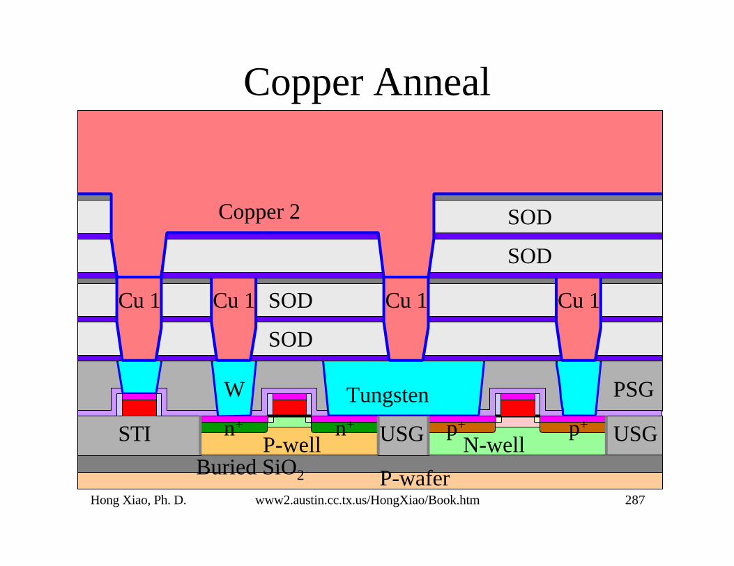
Copper Anneal
P-well
P-waferBuried SiO2
USGN-wellSTI USGn+ n+ p+ p+
PSGW Tungsten
SOD
SODCu 1 Cu 1 Cu 1 Cu 1
SOD
SODCopper 2
Hong Xiao, Ph. D. www2.austin.cc.tx.us/HongXiao/Book.htm 288
P-well
P-waferBuried SiO2
USGN-wellSTI USGn+ n+ p+ p+
PSGW Tungsten
SOD
SODCu 1 Cu 1 Cu 1 Cu 1
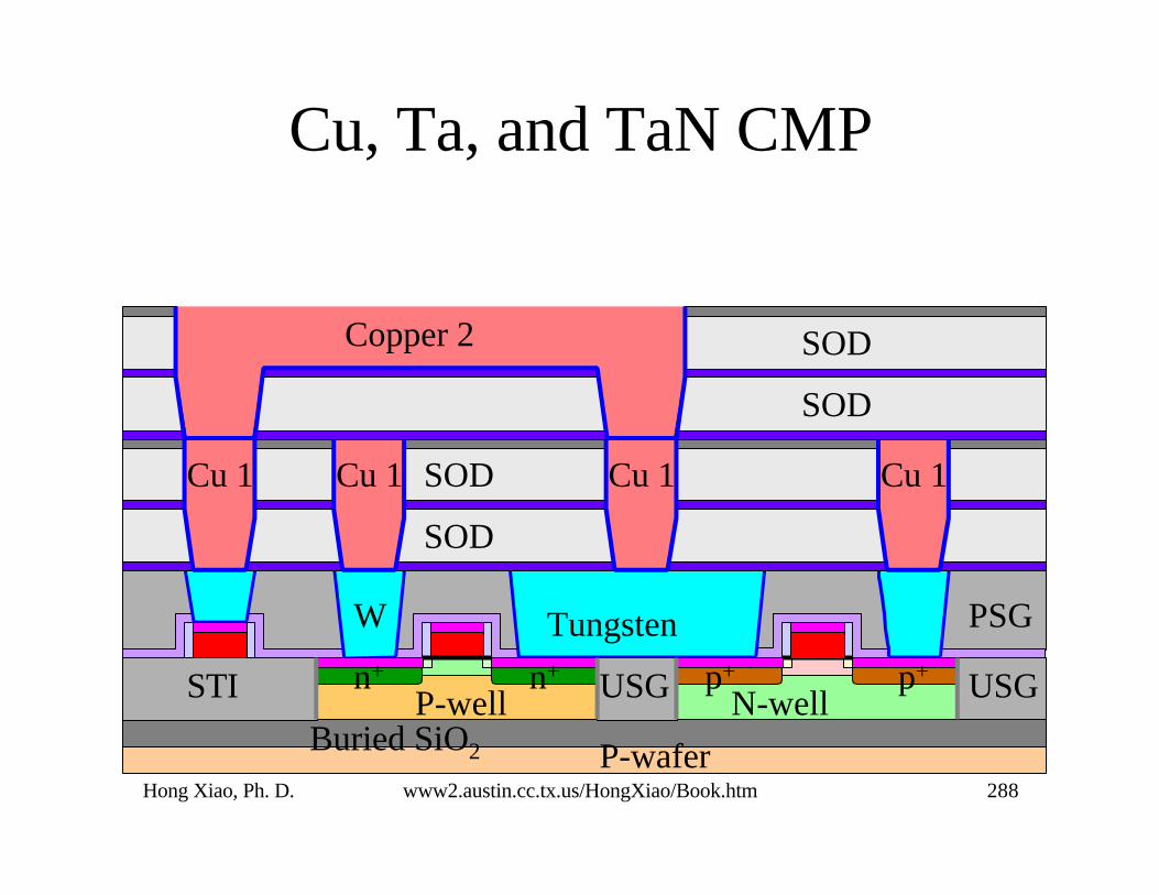
Cu, Ta, and TaN CMP
SOD
SODCopper 2
Hong Xiao, Ph. D. www2.austin.cc.tx.us/HongXiao/Book.htm 289
P-well
P-waferBuried SiO2
USGN-wellSTI USGn+ n+ p+ p+
PSGW Tungsten
SOD
SODCu 1 Cu 1 Cu 1 Cu 1
SOD
SODCopper 2
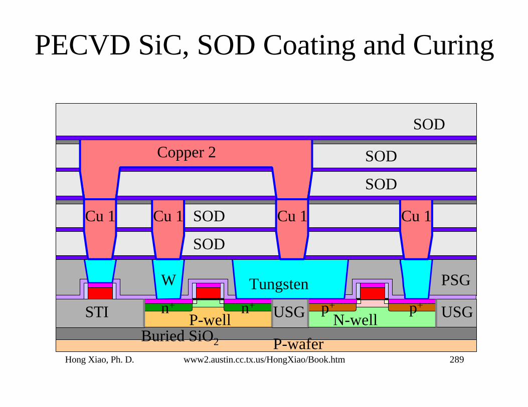
PECVD SiC, SOD Coating and Curing
SOD

Hong Xiao, Ph. D. www2.austin.cc.tx.us/HongXiao/Book.htm 290
P-well
P-waferBuried SiO2
USGN-wellSTI USGn+ n+ p+ p+
PSGW Tungsten
SOD
SODCu 1 Cu 1 Cu 1 Cu 1
SOD
SODCopper 2
PECVD SiC Etch Stop Layer
SOD

Hong Xiao, Ph. D. www2.austin.cc.tx.us/HongXiao/Book.htm 291
P-well
P-waferBuried SiO2
USGN-wellSTI USGn+ n+ p+ p+
PSGW Tungsten
SOD
SODCu 1 Cu 1 Cu 1 Cu 1
SOD
SODCopper 2
Photoresist Coating and Baking
SOD
Photoresist

Hong Xiao, Ph. D. www2.austin.cc.tx.us/HongXiao/Book.htm 292
Mask 14, Via 3

Hong Xiao, Ph. D. www2.austin.cc.tx.us/HongXiao/Book.htm 293
P-well
P-waferBuried SiO2
USGN-wellSTI USGn+ n+ p+ p+
PSGW Tungsten
SOD
SODCu 1 Cu 1 Cu 1 Cu 1
SOD
SODCopper 2
Alignment and Exposure
SOD
Photoresist

Hong Xiao, Ph. D. www2.austin.cc.tx.us/HongXiao/Book.htm 294
P-well
P-waferBuried SiO2
USGN-wellSTI USGn+ n+ p+ p+
PSGW Tungsten
SOD
SODCu 1 Cu 1 Cu 1 Cu 1
SOD
SODCopper 2
PEB, Development, and Inspection
SOD
Photoresist

Hong Xiao, Ph. D. www2.austin.cc.tx.us/HongXiao/Book.htm 295
P-well
P-waferBuried SiO2
USGN-wellSTI USGn+ n+ p+ p+
PSGW Tungsten
SOD
SODCu 1 Cu 1 Cu 1 Cu 1
SOD
SODCopper 2
Etch SiC
SOD
Photoresist
Hong Xiao, Ph. D. www2.austin.cc.tx.us/HongXiao/Book.htm 296
P-well
P-waferBuried SiO2
USGN-wellSTI USGn+ n+ p+ p+
PSGW Tungsten
SOD
SODCu 1 Cu 1 Cu 1 Cu 1
SOD
SODCopper 2
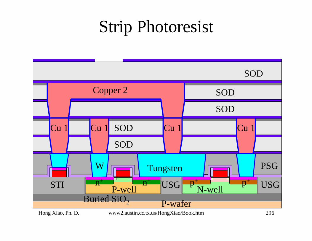
Strip Photoresist
SOD
Hong Xiao, Ph. D. www2.austin.cc.tx.us/HongXiao/Book.htm 297
P-well
P-waferBuried SiO2
USGN-wellSTI USGn+ n+ p+ p+
PSGW Tungsten
SOD
SODCu 1 Cu 1 Cu 1 Cu 1
SOD
SODCopper 2
SOD
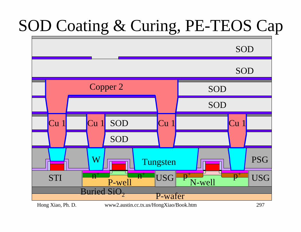
SOD Coating & Curing, PE-TEOS Cap
SOD

Hong Xiao, Ph. D. www2.austin.cc.tx.us/HongXiao/Book.htm 298
P-well
P-waferBuried SiO2
USGN-wellSTI USGn+ n+ p+ p+
PSGW Tungsten
SOD
SODCu 1 Cu 1 Cu 1 Cu 1
SOD
SODCopper 2
SOD
Photoresist Coating and Baking
SOD
Hong Xiao, Ph. D. www2.austin.cc.tx.us/HongXiao/Book.htm 299
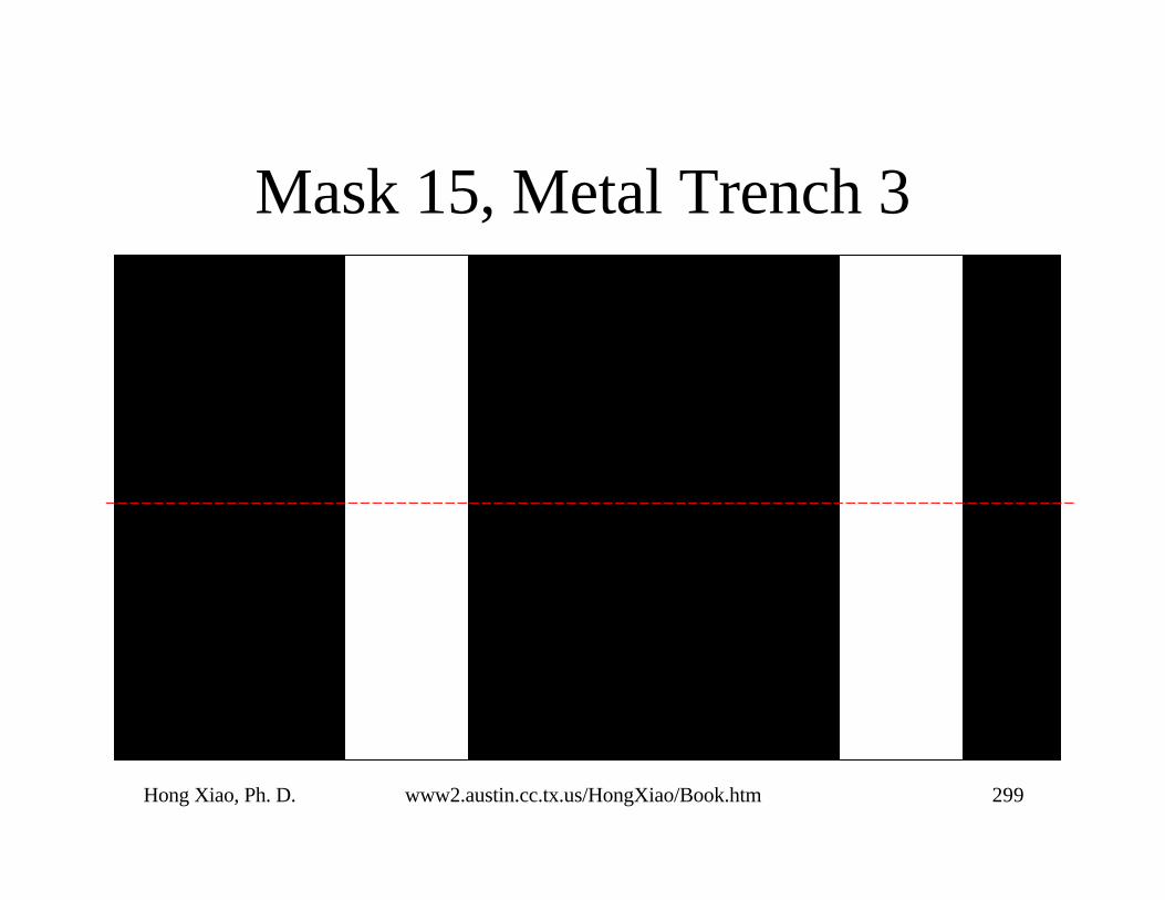
Mask 15, Metal Trench 3

Hong Xiao, Ph. D. www2.austin.cc.tx.us/HongXiao/Book.htm 300
P-well
P-waferBuried SiO2
USGN-wellSTI USGn+ n+ p+ p+
PSGW Tungsten
SOD
SODCu 1 Cu 1 Cu 1 Cu 1
SOD
SODCopper 2
SOD
SOD
Alignment and Exposure

Hong Xiao, Ph. D. www2.austin.cc.tx.us/HongXiao/Book.htm 301
P-well
P-waferBuried SiO2
USGN-wellSTI USGn+ n+ p+ p+
PSGW Tungsten
SOD
SODCu 1 Cu 1 Cu 1 Cu 1
SOD
SODCopper 2
SOD
SOD
PEB, Development, and Inspection
Hong Xiao, Ph. D. www2.austin.cc.tx.us/HongXiao/Book.htm 302
P-well
P-waferBuried SiO2
USGN-wellSTI USGn+ n+ p+ p+
PSGW Tungsten
SOD
SODCu 1 Cu 1 Cu 1 Cu 1
SOD
SODCopper 2
SOD
SOD
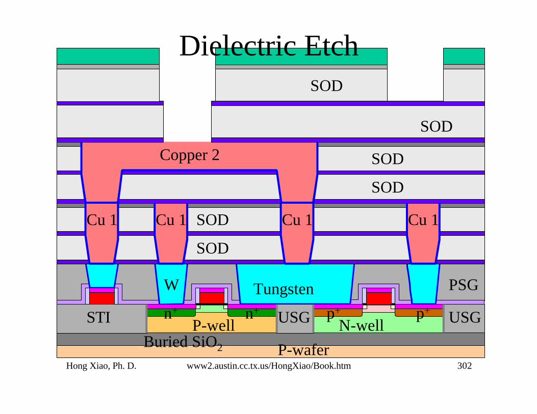
Dielectric Etch

Hong Xiao, Ph. D. www2.austin.cc.tx.us/HongXiao/Book.htm 303
P-well
P-waferBuried SiO2
USGN-wellSTI USGn+ n+ p+ p+
PSGW Tungsten
SOD
SODCu 1 Cu 1 Cu 1 Cu 1
SOD
SODCopper 2
SOD
SOD
Strip Photoresist

Hong Xiao, Ph. D. www2.austin.cc.tx.us/HongXiao/Book.htm 304
P-well
P-waferBuried SiO2
USGN-wellSTI USGn+ n+ p+ p+
PSGW Tungsten
SOD
SODCu 1 Cu 1 Cu 1 Cu 1
SOD
SODCopper 2
SOD
SOD
Hydrogen Plasma Clean

Hong Xiao, Ph. D. www2.austin.cc.tx.us/HongXiao/Book.htm 305
P-well
P-waferBuried SiO2
USGN-wellSTI USGn+ n+ p+ p+
PSGW Tungsten
SOD
SODCu 1 Cu 1 Cu 1 Cu 1
SOD
SODCopper 2
SOD
SOD
Cu, Ta, and TaN Deposition and CMPCu 3 Cu 3
Hong Xiao, Ph. D. www2.austin.cc.tx.us/HongXiao/Book.htm 306
SOD
SOD
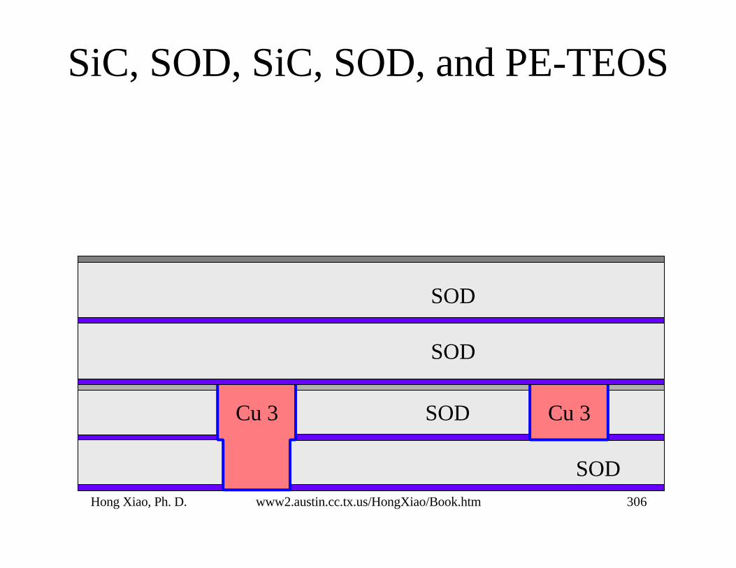
SiC, SOD, SiC, SOD, and PE-TEOS
Cu 3 Cu 3
SOD
SOD
Hong Xiao, Ph. D. www2.austin.cc.tx.us/HongXiao/Book.htm 307
SOD
SOD
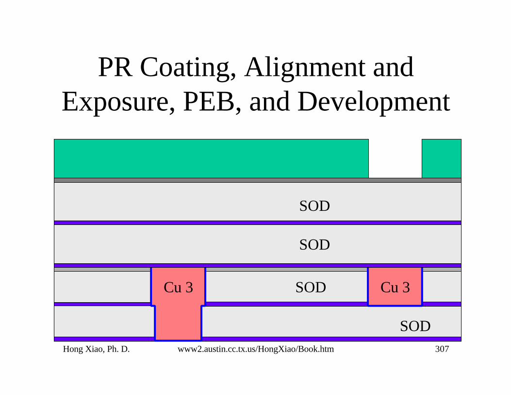
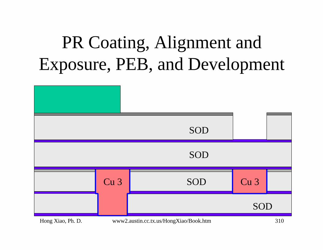
PR Coating, Alignment andExposure, PEB, and Development
Cu 3 Cu 3
SOD
SOD

Hong Xiao, Ph. D. www2.austin.cc.tx.us/HongXiao/Book.htm 308
SOD
SOD
Via 4 Etch
Cu 3 Cu 3
SOD
SOD

Hong Xiao, Ph. D. www2.austin.cc.tx.us/HongXiao/Book.htm 309
SOD
SOD
Strip Photoresist
Cu 3 Cu 3
SOD
SOD
Hong Xiao, Ph. D. www2.austin.cc.tx.us/HongXiao/Book.htm 310
SOD
SOD
PR Coating, Alignment andExposure, PEB, and Development
Cu 3 Cu 3
SOD
SOD

Hong Xiao, Ph. D. www2.austin.cc.tx.us/HongXiao/Book.htm 311
SOD
SOD
Etch Trench
Cu 3 Cu 3
SOD
SOD
Hong Xiao, Ph. D. www2.austin.cc.tx.us/HongXiao/Book.htm 312
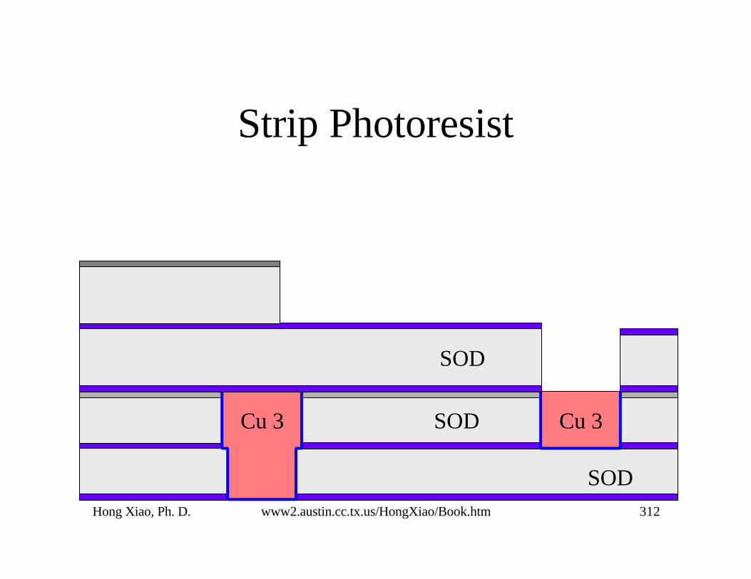
SOD
SOD
Strip Photoresist
Cu 3 Cu 3
SOD
SOD

Hong Xiao, Ph. D. www2.austin.cc.tx.us/HongXiao/Book.htm 313
SOD
SOD
Hydrogen Plasma Clean
Cu 3 Cu 3
SOD
SOD
Hong Xiao, Ph. D. www2.austin.cc.tx.us/HongXiao/Book.htm 314
SOD
SOD
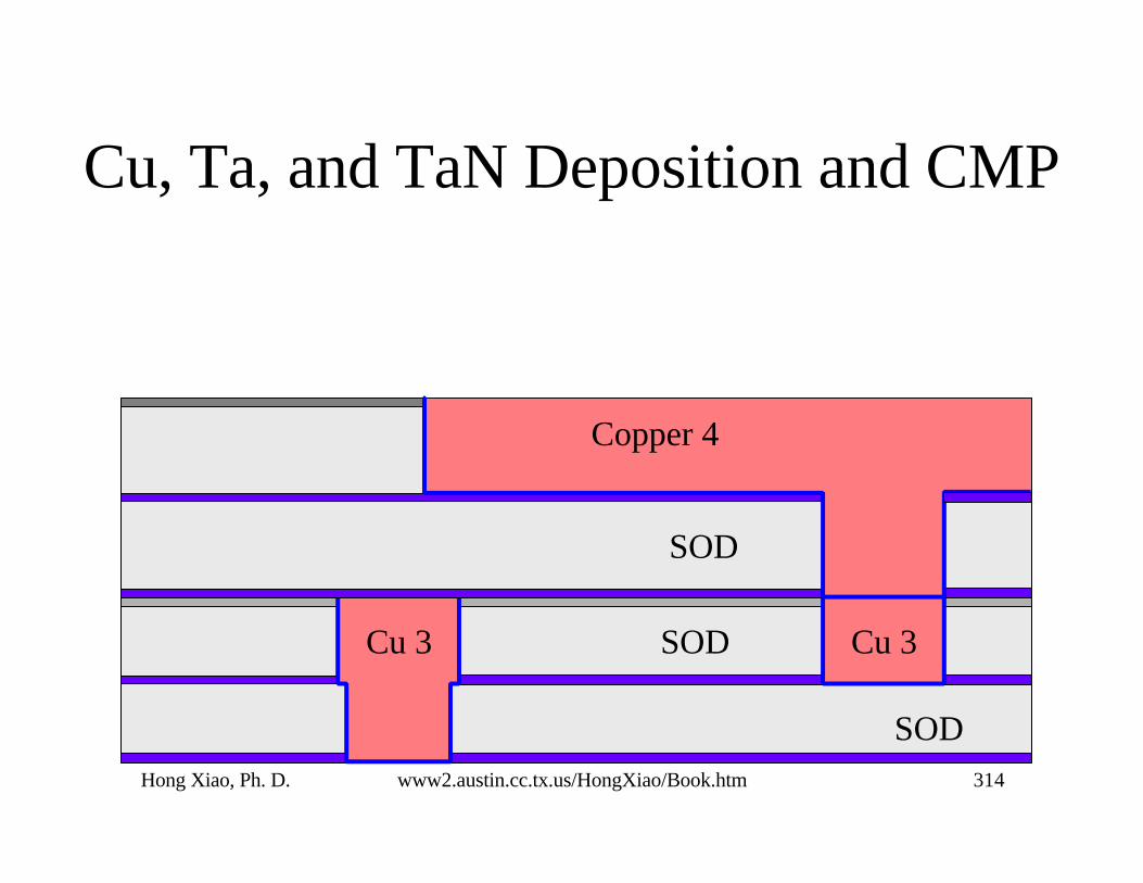
Cu, Ta, and TaN Deposition and CMP
Cu 3 Cu 3
SOD
SOD Copper 4
Hong Xiao, Ph. D. www2.austin.cc.tx.us/HongXiao/Book.htm 315
SOD
SOD
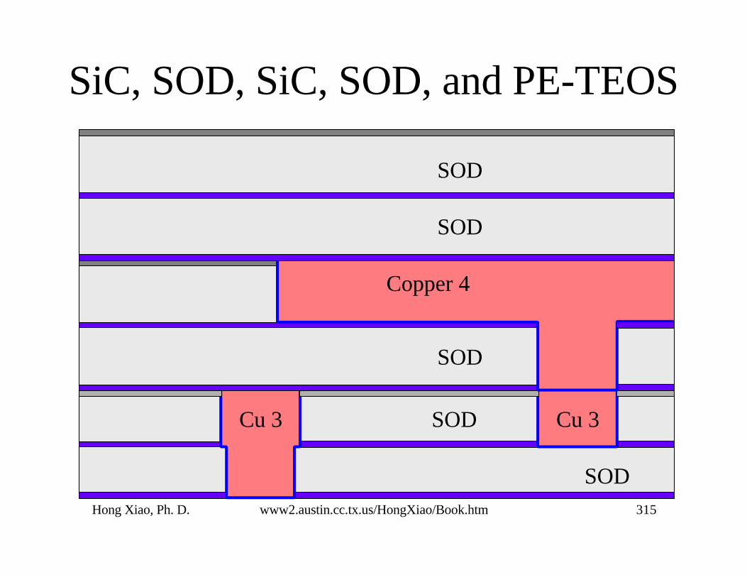
SiC, SOD, SiC, SOD, and PE-TEOS
Cu 3 Cu 3
SOD
SOD
SOD
SOD Copper 4
Hong Xiao, Ph. D. www2.austin.cc.tx.us/HongXiao/Book.htm 316
SOD
SOD
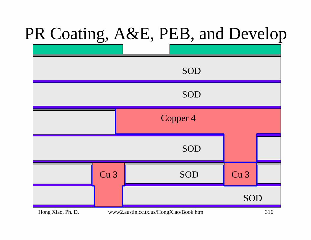
PR Coating, A&E, PEB, and Develop
Cu 3 Cu 3
SOD
SOD
SOD
SOD Copper 4

Hong Xiao, Ph. D. www2.austin.cc.tx.us/HongXiao/Book.htm 317
SOD
SOD
Etch Via5
Cu 3 Cu 3
SOD
SOD
SOD
SOD Copper 4

Hong Xiao, Ph. D. www2.austin.cc.tx.us/HongXiao/Book.htm 318
SOD
SOD
Strip Photoresist
Cu 3 Cu 3
SOD
SOD
SOD
SOD Copper 4

Hong Xiao, Ph. D. www2.austin.cc.tx.us/HongXiao/Book.htm 319
SOD
SOD
PR Coating, A&E, PEB, and Develop
Cu 3 Cu 3
SOD
SOD
SOD
SOD Copper 4

Hong Xiao, Ph. D. www2.austin.cc.tx.us/HongXiao/Book.htm 320
SOD
SOD
Dielectric Etch
Cu 3 Cu 3
SOD
SOD
SOD
SOD Copper 4

Hong Xiao, Ph. D. www2.austin.cc.tx.us/HongXiao/Book.htm 321
SOD
SOD
Strip Photoresist
Cu 3 Cu 3
SOD
SOD
SOD
SOD Copper 4

Hong Xiao, Ph. D. www2.austin.cc.tx.us/HongXiao/Book.htm 322
SOD
SOD
Hydrogen Plasma Clean
Cu 3 Cu 3
SOD
SOD
SOD
SOD Copper 4

Hong Xiao, Ph. D. www2.austin.cc.tx.us/HongXiao/Book.htm 323
SOD
SOD
Cu, Ta, and TaN Deposition and CMP
Cu 3 Cu 3
SOD
SODCopper 5
SOD
SOD Copper 4

Hong Xiao, Ph. D. www2.austin.cc.tx.us/HongXiao/Book.htm 324
PECVD Passivation Layers:Nitride, PSG, and Nitride
SOD
SODCopper 5
PSG
Nitride

Hong Xiao, Ph. D. www2.austin.cc.tx.us/HongXiao/Book.htm 325
PR Coating, A&E, PEB, and Develop
SOD
SODCopper 5
PSG
Nitride

Hong Xiao, Ph. D. www2.austin.cc.tx.us/HongXiao/Book.htm 326
Etch Passivation Layers
SOD
SODCopper 5
PSG
Nitride

Hong Xiao, Ph. D. www2.austin.cc.tx.us/HongXiao/Book.htm 327
Strip Photoresist
SOD
SODCopper 5
PSG
Nitride

Hong Xiao, Ph. D. www2.austin.cc.tx.us/HongXiao/Book.htm 328
Polyamide Coating
SOD
SODCopper 5
PSG
Nitride
Polyamide

Hong Xiao, Ph. D. www2.austin.cc.tx.us/HongXiao/Book.htm 329
Ship to Test and Package
SOD
SODCopper 5
PSG
Nitride
Polyamide
Hong Xiao, Ph. D. www2.austin.cc.tx.us/HongXiao/Book.htm 330
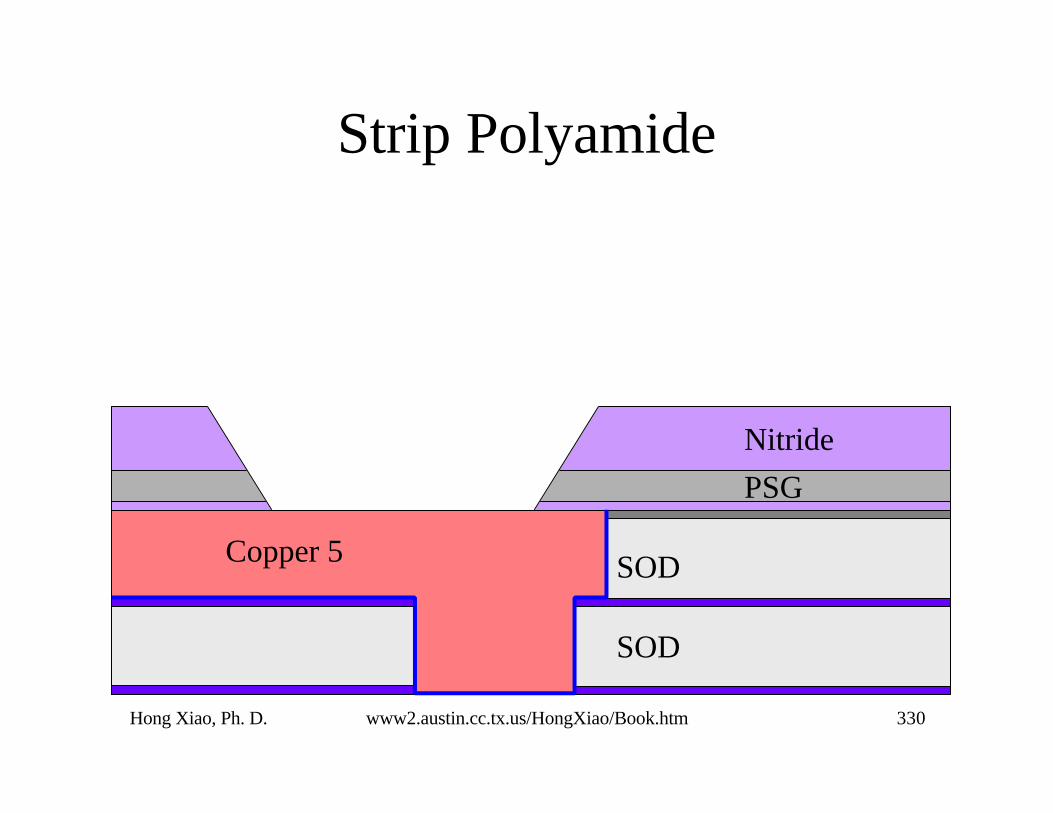
Strip Polyamide
SOD
SODCopper 5
PSG
Nitride

Hong Xiao, Ph. D. www2.austin.cc.tx.us/HongXiao/Book.htm 331
Argon Sputtering Etch
SOD
SODCopper 5
PSG
Nitride

Hong Xiao, Ph. D. www2.austin.cc.tx.us/HongXiao/Book.htm 332
Cr, Cu, and Au Liner Coating
SOD
SODCopper 5
PSG
Nitride

Hong Xiao, Ph. D. www2.austin.cc.tx.us/HongXiao/Book.htm 333
Lead-Tin Alloy Coating
SOD
SODCopper 5
PSG
NitrideLead-tin alloy

Hong Xiao, Ph. D. www2.austin.cc.tx.us/HongXiao/Book.htm 334
PR Coating, A&E, PEB, and Develop
SOD
SODCopper 5
PSG
NitrideLead-tin alloy
Photoresist

Hong Xiao, Ph. D. www2.austin.cc.tx.us/HongXiao/Book.htm 335
Metal Etch
SOD
SODCopper 5
PSG
NitrideLead-tin alloy
Photoresist
Hong Xiao, Ph. D. www2.austin.cc.tx.us/HongXiao/Book.htm 336
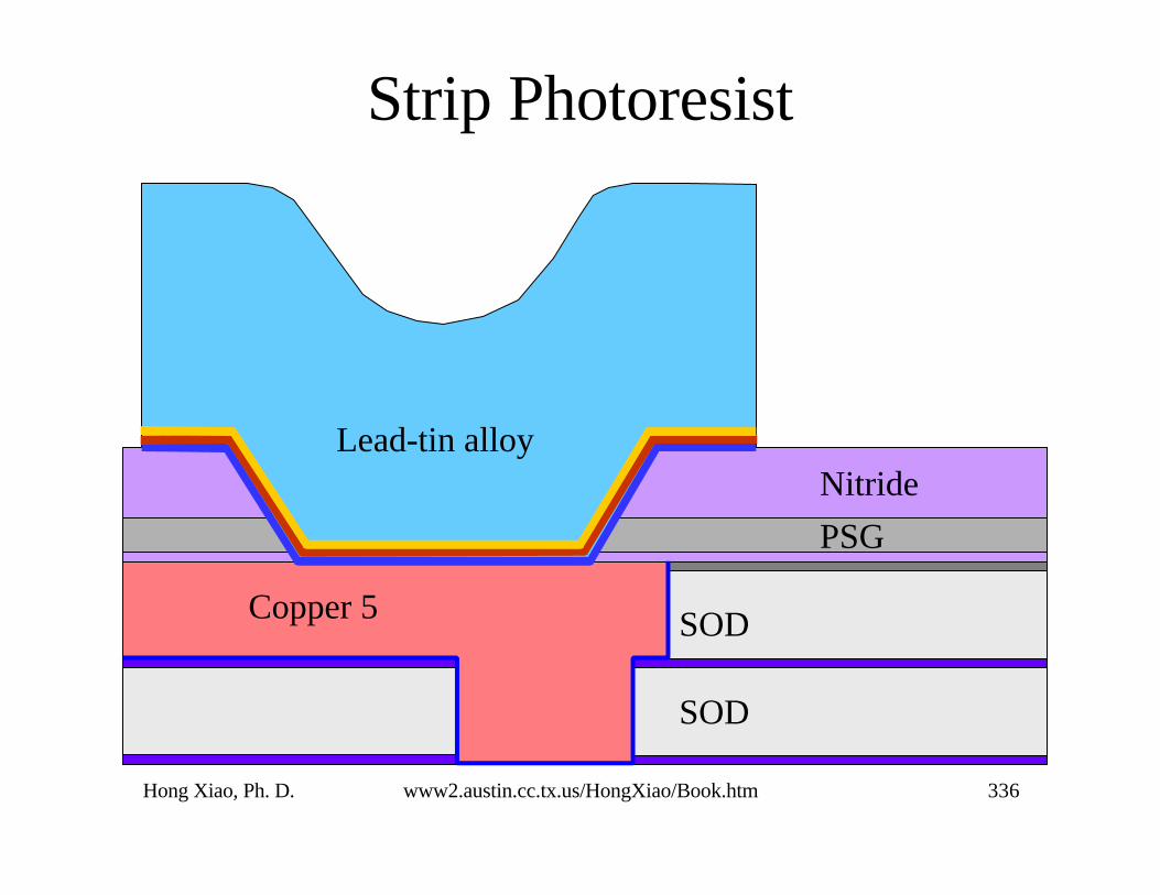
Strip Photoresist
SOD
SODCopper 5
PSG
NitrideLead-tin alloy
Hong Xiao, Ph. D. www2.austin.cc.tx.us/HongXiao/Book.htm 337
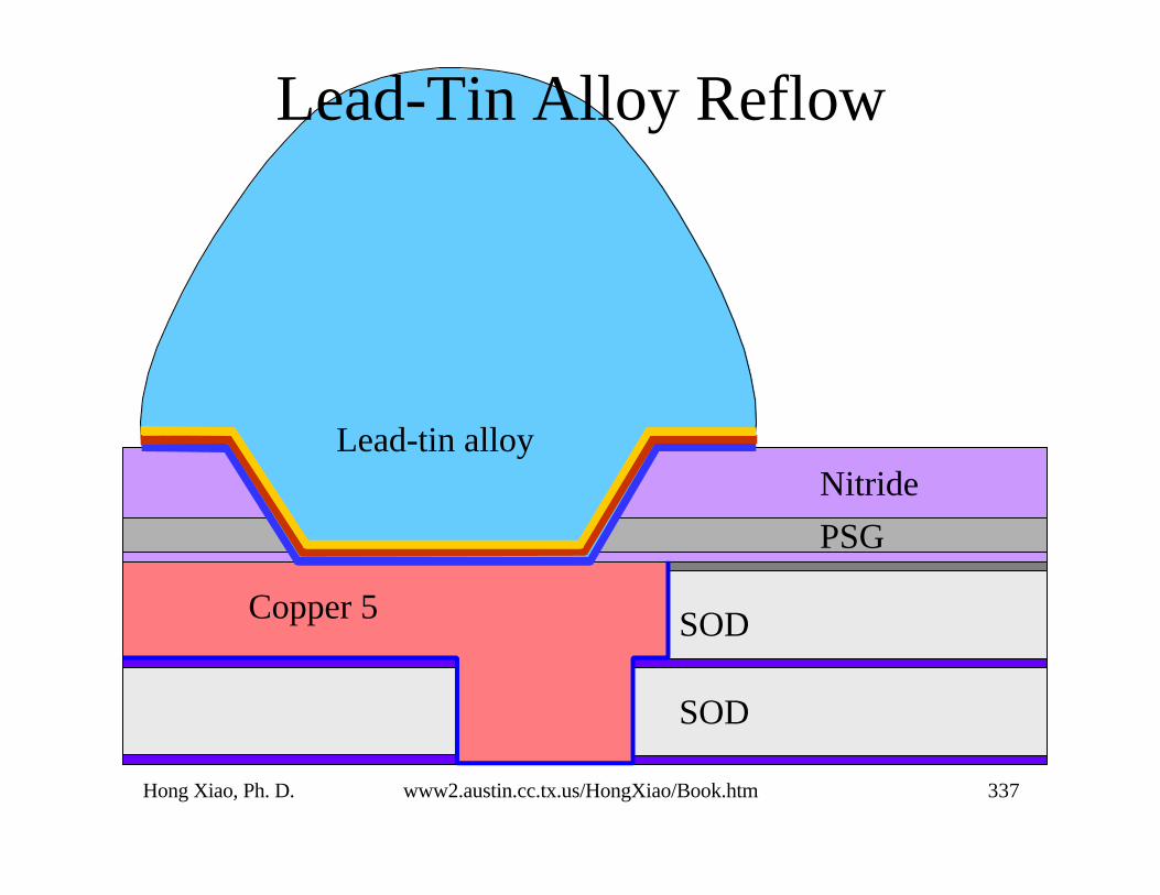
Lead-Tin Alloy Reflow
SOD
SODCopper 5
PSG
NitrideLead-tin alloy
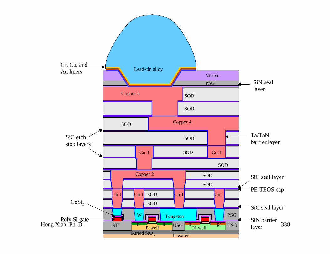
Hong Xiao, Ph. D. www2.austin.cc.tx.us/HongXiao/Book.htm 338P-well
P-waferBuried SiO 2
USGN-wellSTI USGn+ n+ p+ p+
PSGW Tungsten
SOD
SODCu 1Cu 1 Cu 1Cu 1 Cu 1Cu 1 Cu 1Cu 1
SOD
SODCopper 2
SOD
SOD
Cu 3 Cu 3
SOD
Copper 4
SOD
SODCopper 5
PSG
NitrideLead-tin alloy
SOD
SiC seal layer
SiN barrierlayer
PE-TEOS cap
SiC seal layer
SiN seallayer
Ta/TaNbarrier layer
SiC etchstop layers
Poly Si gate
CoSi2
Cr, Cu, andAu liners
Hong Xiao, Ph. D. www2.austin.cc.tx.us/HongXiao/Book.htm 339
Summary
• CMOS IC chips dominate semiconductorindustry– Demands for digital electronics, such as
electronic watches, calculators, and personalcomputers
Hong Xiao, Ph. D. www2.austin.cc.tx.us/HongXiao/Book.htm 340
Summary
• In the 1980s– 3 micron to sub-micron
– Multi-layer metallization
– Tungsten CVD, dielectric CVD and metal sputtering
– Sidewall spacer for LDD
– Plasma etch gradually replaced wet etch in allpatterning etch processes.
– Steppers became popular for alignment and exposurewhile projection systems were widely used

Hong Xiao, Ph. D. www2.austin.cc.tx.us/HongXiao/Book.htm 341
Summary
• In the 1990s,– 0.8 micron to 0.18 micron– Silicides used for the gate and local interconnection– CMP widely used for tungsten polishing and dielectric
planarization– RTP is widely used for anneal processes– HDP sources are used for etch, CVD, sputtering clean,
and sputtering deposition– O3-TEOS oxide CVD processes commonly used for
STI, PMD and IMD depositions.– ECP is used for copper metallization process