the future of nano-computing - georgia institute of … - the...the future of nano-computing george...
TRANSCRIPT

2/5/2003 Intel Corp. George Bourianoff 1
The future of nano-computing
George BourianoffIntel Corporation
Presented toInternational Engineering Consortium and
Electrical and Computer Engineering Department Heads
Jan. 27, 2003 San Jose, Ca

2/5/2003 Intel Corp. George Bourianoff 2
Future of Nanocomputing
Silicon highway
Scalable newtechnology
Scalable newtechnology
originscharacteristics
limits
criteria
criteria
taxonomyelements

2/5/2003 Intel Corp. George Bourianoff 3
Key messages
• CMOS scaling will continue for next 12 –15 years
• Alternative new technologies will emerge and begin to be integrated on CMOS by 2015
• Nanoscience research is needed to facilitate radical new scalable technologies beyond 2020

2/5/2003 Intel Corp. George Bourianoff 4
The future of nanocomputing
• Introduction• Scaled CMOS• Nano-computing, nano-technology and
nano-science• Radical new technologies• Challenges• Conclusions
2/5/2003 Intel Corp. George Bourianoff 5
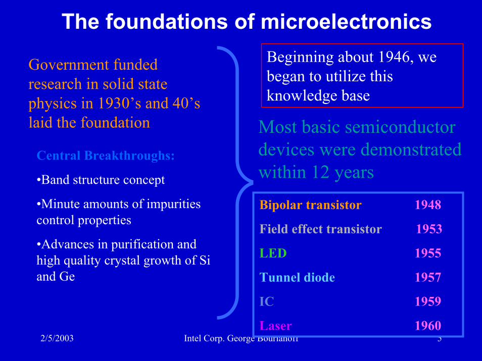
The foundations of microelectronics
Central Breakthroughs:
•Band structure concept
•Minute amounts of impurities control properties
•Advances in purification and high quality crystal growth of Siand Ge
Most basic semiconductor devices were demonstrated within 12 years
Beginning about 1946, we began to utilize this knowledge base
Government funded research in solid state physics in 1930’s and 40’s laid the foundation
Bipolar transistor 1948
Field effect transistor 1953
LED 1955
Tunnel diode 1957
IC 1959
Laser 1960

2/5/2003 Intel Corp. George Bourianoff 6
The beauty of silicon
1 GB64 MB4 MBDRAMs
Cost per Megabit
12”8”6”Wafer diameter
0.15 µm0.35 µm0.8 µmFeature size
200019951990
1. Scaling device dimensions downward
For four decades, the semiconductor industry has steadily reduced the unit cost of IC components by
$6.50 $3.14 $0.10
2. Scaling wafer diameter upward

2/5/2003 Intel Corp. George Bourianoff 7
200870 nm
201150 nm
201435 nm
6.00 10.00 13.509 9-10 103 4 4
2.1 E6 3.7 E6 4.6 E6140 100 70165 120 851.9 2.1 2.2 - 2.39 7 5
210 145 1102.5/2.3 2.7/2.4 2.9/2.5
30 22 17
0 0 0330 240 170
2.8/2.9 2.9/3.0 3.0/3.155 38 20
14.1 16.1 23.11.8 < 1.8 < 1.80 0 0
1.4 <1.5 <1.5
Brick Walls on the ITRSYEAR
TECHNOLOGY NODE1999
180 nm2002
130 nm2005
100 nmOn-chip local frequency (MHz) 1.25 2.10 3.50Number of metal levels - Logic 6-7 7-8 8-9Number of optional levels 0 2 2Jmax (A/cm2) - wire (at 105oC) 5.8 E5 9.6 E5 1.4 E6Local wiring pitch - DRAM non-contacted (nm) 360 260 200Local wiring pitch - Logic (nm) 500 325 230Local wiring AR-Logic (Cu) 1.4 1.5 1.7Cu local dishing (nm) 18 14 11Intermediate wiring pitch - Logic (nm) 560 405 285Intermediate wiring h/w AR - Logic (Cu DD via/lin) 2.0/2.1 2.2/2.1 2.4/2.2Cu intermediate wiring dishing - 15 um wide wire (nm) 64 51 41Dielectric erosion, intermediate wiring 50% density (nm) 64 51 41Global wiring pitch - Logic (nm) 900 650 460Global wiring h/w AR - Logic - Cu DD via/line (nm) 2.2/2.4 2.5/2.7 2.7/2.8Cu global wiring dishing, 15 um wide wire (nm) 116 95 76Contact aspect ratio - DRAM, stacked cap 9.3 11.4 13Conductor effective resistivity (uohm -cm) 2.2 2.2 2.2Barrier/cladding thickness (nm) 17 13 10Interlevel metal insulator effective dielectric constant (k) - Logic 4.0 - 3.5 3.5 - 2.7 2.2 - 1.6
Solutions ExistSolutions being pursuedNo known solutions
200870 nm
201150 nm
201435 nm
6.00 10.00 13.509 9-10 103 4 4
2.1 E6 3.7 E6 4.6 E6140 100 70165 120 851.9 2.1 2.2 - 2.39 7 5
210 145 1102.5/2.3 2.7/2.4 2.9/2.5
30 22 17
0 0 0330 240 170
2.8/2.9 2.9/3.0 3.0/3.155 38 20
14.1 16.1 23.11.8 < 1.8 < 1.80 0 0
1.4 <1.5 <1.5

2/5/2003 Intel Corp. George Bourianoff 8
Silicon Nanotechnology is Here!1000010000
10001000
100100
1010
1010
11
0.10.1
0.010.01
MicronMicron NanoNano--metermeter
1970 1980 1990 2000 2010 20201970 1980 1990 2000 2010 2020
Nominal feature sizeNominal feature size
NanotechnologyNanotechnology
130nm130nm90nm90nm
70nm70nm50nm50nm
Gate WidthGate Width

2/5/2003 Intel Corp. George Bourianoff 9
The ingredients of scaling Material Evolution in MOSMaterial Evolution in MOS
2000’s
60’s70’s
80’s
90’s
Al
SiO2
Al-Si
SiO2
Poly
Al-Cu
SiO2
WSi2/Poly
Ti/TiN
Al-Cu
SiO2
TiSi2/Poly
Ti/TiN
W
Al-Cu
SiO2
TiSi2/Poly
Ti/TiN
W
Low K
Al-Cu
SiO2/SiN
CSi2/Poly
Ti/TiN
W
ELK
Cu
Silicon Silicon Silicon Silicon Silicon Silicon
New materials
Improved processing
New geometries
Scaling Will continue as long as (δ cost) /(δ performance) < alternate technologies

2/5/2003 Intel Corp. George Bourianoff 10
Transistor Scaling
70nm transistorfor 0.13µm process
2001 production
70nm
30nm transistor Prototype
30nm
Demo: 2000
15nm15nm transistor
prototype Source: Intel (IEDM, Dec 2001)
0
100200
300400
500
0 0.2 0.4 0.6 0.8Drain Voltage (V)
Dra
in C
urre
nt (µ
A/µm
)
Vg = 0.8V
0.7V
0.6V
0.5V0.4V0.3V
15nm NMOS
100nm100nm
Influenza virusSource: CDC

2/5/2003 Intel Corp. George Bourianoff 11
New Materials
GateGateSilicideSilicideaddedadded
ChannelChannelStrainedStrainedsiliconsilicon
ChangesChangesMadeMade
FutureFutureOptionsOptions
HighHigh--kkgategate
dielectricdielectric
NewNewtransistortransistorstructurestructure
TransistorTransistorSource: Intel
The problem: High Ioff currentThe problem: High The problem: High IoffIoff currentcurrent

2/5/2003 Intel Corp. George Bourianoff 12
New Geometries
SourceSourceDrainDrain
GateGate
GateGate
SiliconSilicon
DrainDrain
SourceSource
00 0.30.3 0.60.6 0.90.9 1.21.2
Id (
Id ( m
Am
A/µ
m)
/µm
)
00 0.30.3 0.60.6 0.90.9 1.21.2VdVd (V) (V)
0.20.2
0.40.4
0.60.6
0.80.8
1.01.0
1.21.2
Source: Intel Source: Intel (ISSDM, Sep 2002)(ISSDM, Sep 2002)
Source: Intel

2/5/2003 Intel Corp. George Bourianoff 13
Improved processing
EUV EUV LithographyLithographyPrototype Exposure ToolPrototype Exposure Tool
50nm Lines Printed50nm Lines Printedwith EUV Lithographywith EUV Lithography
EUV lithography in commercialization phaseCost effectiveness is key challenge
EUV lithography in commercialization phaseCost effectiveness is key challenge
Source: Source: SandiaSandia

2/5/2003 Intel Corp. George Bourianoff 14
The limits of logic scaling
• For an arbitrary switching device made of of a single electron in a dual quantum well– Operating at room temperature
• It can be shown a power dissipation limit of 100 W/cm**2
• Will limit the operational frequency to ~100 GHz at length scales ~ 4 nm

2/5/2003 Intel Corp. George Bourianoff 15
CMOS device circa 2016
• Cost 10-11 $/gate
• Size 8 nm / device
• Speed 0.2 ps /operation
• Energy 10-18 J/operation

2/5/2003 Intel Corp. George Bourianoff 16
The future of nanocomputing
– Introduction– Scaled CMOS– Nano-computing, nano-technology and nano-science
• A taxonomy• New devices• New architectures• Alternative state variables
– Radical new technologies– Challenges– Conclusions

2/5/2003 Intel Corp. George Bourianoff 17
Architecture
Devices
State variables
Data represent
ations
A taxonomy for nano-computing
CNT FETs
Molecular Spintronics Quantum
CNN Crossbar QuantumBoolean
Molecular state
Spin orientation
Flux quanta Quantum stateElectric charge
associativepatterns
analogue
Digital
Scaled CMOS
probabilities
Heir-archy
biotech
Memory devices sensors
Time

2/5/2003 Intel Corp. George Bourianoff 18
The future of nanocomputing– Introduction– Scaled CMOS– Nano-computing, nano-technology and nano-science
• A taxonomy• New devices• New architectures• Alternative state variables
– Radical new technologies– Challenges– Conclusions

2/5/2003 Intel Corp. George Bourianoff 19

2/5/2003 Intel Corp. George Bourianoff 20
CNT-FET Device StructureE-beam Ti/Au gate
Mo S/D 8 nmZrO2
1.4 nm diameter single wall CNT
McEuen et. al, . Cornell Universwity

2/5/2003 Intel Corp. George Bourianoff 21
Nanowire Gating Geometries
S
D
GSiO2
Si
Back gate
S
DGTop gate
S
D
GCoaxial gateC. Leiber et. al. , Harvard U

2/5/2003 Intel Corp. George Bourianoff 22
Top-gated p-Si Nanowire Transistors
S
DG
1500
1000
500
0
-I DS (n
A)
-2 -1 0 1 2VGS (V)
0.01
0.1
1
10
100
1000
-IDS (nA)
700 nA/V
250 mV/dec
VDS= -1 V
-2.5
-2.0
-1.5
-1.0
-0.5
0.0
I DS
(µA)
-4 -3 -2 -1 0VDS (V)
-2.0 VGS
-1.5 VGS
-1.0 VGS
-0.5 VGS
0.0 VGS
+0.5 VGS
Si
SiOx
D
S
G
1 µm
1 µm
C. Leiber et. al. , Harvard U

2/5/2003 Intel Corp. George Bourianoff 23
Crossed Nanowire Structures: A Powerful Strategy for Creation &
Integration of Nanodevices
Nanowires serve dual purpose: both active devices and interconnects.All key nanoscale metrics are defined during synthesis and subsequent assembly. Crossed nanowire architecture provides natural scaling and potential for integration at highest densities.No additional complexity (with added material).C. Leiber et. al. , Harvard U

2/5/2003 Intel Corp. George Bourianoff 24
Crossed Nanowire FETs
400
200
0
-200
-400
Cur
rent
(nA
)
-1.0 -0.5 0.0 0.5 1.0Bias (V)
S D
G
Vg(V):0
1
23
10-2
100
102
Cur
rent
(nA
)
543210Gate (V)
In crossed nanowire FETs (cNW-FET), all critical nanoscale metrics are defined by synthesis and assembly:
• channel width by the active nanowire diameter (to 2 nm)• channel length by the gate nanowire diameter (to 1-2 nm)• gate dielectric oxide coating on the nanowires (to 1 atomic layer)
The conductance of cNW-FETs can be changed by more than 105-times with less than 0.1 V variation in the nano-gate.
Huang, Duan, Lieber et al., Science 294, 1313 (2001)

2/5/2003 Intel Corp. George Bourianoff 25
Device DemonstratedP-N Junction
Lieber/Harvard

2/5/2003 Intel Corp. George Bourianoff 26
Room temperature Single Electron Transistor (SET)
••Single electron Single electron in “island” in “island” controls current controls current flow from flow from source to drainsource to drain
••Typical sizes Typical sizes of theof the TiOxTiOxlines are 15lines are 15--25 25 nm widths and nm widths and 3030--50 nm 50 nm lengths. lengths.
••Typical island Typical island sizes are 30sizes are 30--50 50 nm by 35nm by 35--50 50 nmnm Courtesy, NEC, IEDM 2000, PP 481

2/5/2003 Intel Corp. George Bourianoff 27
Spin resonance transistor (SRT)
• Transistors that control spins rather than charge
• More energy efficient than conventional transistors
• Combines magnetic and electrostatic fields
• May enable quantum computing
Courtesy Eli Courtesy Eli YablanovitchYablanovitch, UCLA, UCLA

2/5/2003 Intel Corp. George Bourianoff 28
A Molecular Electronic Switch(2-amino-4-ethyinylphenyl-4-ethylphenyl-5-
nitro-1-benzenethiolate)Au
Silicon Nitride
1000 Self AssembledMolecules (SEM)
AuIV Characteristics11
0.00 0.50 1.00 1.50 2.00 2.50 3.00Voltage (V)
Cur
rent
(pA)
Source: M.Reed & others,Yale Univ and Rice Univ
(@T=60K)

2/5/2003 Intel Corp. George Bourianoff 29
The future of nanocomputing
– Introduction– Scaled CMOS– Nano-computing, nano-technology and nano-science
• A taxonomy• New devices• New architectures• Alternative state variables
– Radical new technologies– Challenges– Conclusions

2/5/2003 Intel Corp. George Bourianoff 30
Emerging Research Architectures
ARCHITECTURE 3-D INTEGRATION QUANTUM CELLULAR AUTOMATA
DEFECT TOLERANT
ARCHITECTURE
MOLECULAR ARCHITECTURE
CELLULAR NONLINEAR NETWORKS
QUANTUM COMPUTING
DEVICE IMPLEMENTATION
CMOS with dissimilar material systems
Arrays of quantum dots
Intelligently assembles
nanodevices
Molecular switches and
memories
Single electron array
architectures
Spin resonance transistors,
NMR devices, Single flux quantum devices
ADVANTAGES
Less interconnect
delay, Enables mixed
technology solutions
High functional density. No
interconnects in signal path
Supports hardware with
defect densities >50%
Supports memory based
computing
Enables utilization of
single electron devices at
room temperature
Exponential performance
scaling, Enables
unbreakable cryptography
CHALLENGES
Heat removal, No design
tools, Difficult test
and measurement
Limited fan out, Dimensional control (low temperature operation), Sensitive to background
charge
Requires pre-computing test
Limited functionality
Subject to background
noise, Tight
tolerances
Extreme application limitation, Extreme
technology
MATURITY Demonstration Demonstration Demonstration Concept Demonstration Concept
NO 2
H2 N

2/5/2003 Intel Corp. George Bourianoff 31
Quantum Cellular Automata
Adder circuit with carry executed in QCA logic
Example of asynchronous, CNN, nearest neighbor architecture
Courtesy of Notre Dame

2/5/2003 Intel Corp. George Bourianoff 32
Fault tolerant architecture• All-memory architecture• Defect tolerant• Potentially self-repairing and
reconfigurableJ. Heath, R. S. Williams et al, UCLA and HP

2/5/2003 Intel Corp. George Bourianoff 33
Phase logic• Store information in the
relative phase of 2 signals• Multi-valued logic
possible depending on frequencies of 2 signals
• Tunneling Phase logic devices use RTDs to create one of the signals
Courtesy: R Courtesy: R KeihleKeihle, University of , University of MinnesotaMinnesota

2/5/2003 Intel Corp. George Bourianoff 34
Quantum ComputerSelected technological implementations•Liquid-state NMR
•Linear ion trap
•Coupled quantum dots
•Deterministically doped semicondustor structures
31P 31P
e-28SiBarrier layer
- - - + + +A-Gate J-Gate A-Gate

2/5/2003 Intel Corp. George Bourianoff 35
The future of nanocomputing– Introduction– Scaled CMOS– Nano-computing, nano-technology and nano-science
• A taxonomy• New devices• New architectures• Alternative state variables
– Radical new technologies– Challenges– Conclusions

2/5/2003 Intel Corp. George Bourianoff 36
Alternative state variables
• Electric charge
• Molecular state
• Spin orientation
• Electric dipole orientation
• Photon intensity• Photon polarization• Quantum state• Phase state• Mechanical state

2/5/2003 Intel Corp. George Bourianoff 37
The future of nanocomputing– Introduction– Scaled CMOS– Nano-computing, nano-technology and nano-science
• A taxonomy• New devices• New architectures• Alternative state variables
– Radical new technologies– Challenges– Conclusions
2/5/2003 Intel Corp. George Bourianoff 38
Economic criteria
• Economic relevance criteria– The risk adjusted ROI for any new technology must
exceed that of silicon
• Caution– Sufficiently advanced technologies will create their
own applications. New technologies cannot necessarily be justified by current day applications.

2/5/2003 Intel Corp. George Bourianoff 39
Technical criteria
• CMOS compatibility• Energy efficiency• Scalability• Performance• Architectural compatibility• Sensitivity to parametric variation• Room temperature operation• Stability and reliability

2/5/2003 Intel Corp. George Bourianoff 40
Existence proof for alternate models
The brain is the ultimate model for its ability to deal with complexity
• Little understanding on its architecture & organization• It is however
– Orders of magnitude more powerful than the best microprocessor– Self assembled– Parallel operation– Self repairing to a significant degree– Fault tolerant– Runs on ~ 10W

2/5/2003 Intel Corp. George Bourianoff 41
Breakthrough scientific investigation is needed
1952 Achievements• Bulk band structure
of solids
• Doping
• Crystal growth
2002 Needs• geometry dependent
energetic structure of nanostructures
• precise location of atoms
• self organization of matter in complex structures

2/5/2003 Intel Corp. George Bourianoff 42
The integration challenge
ScalabilityScalabilityPort SwitchPort Switch
MemoryMemory MemoryMemoryScalabilityScalability
NodeNodeControllerController
I/O HubI/O Hub
PCIPCI--(X)(X)BridgeBridge
InfiniBand*InfiniBand*BridgeBridge
I/OI/OBridgeBridge
PCIPCI--(X)(X)BridgeBridge
InfiniBand*InfiniBand*BridgeBridge
I/OI/OBridgeBridge
ScalabilityScalabilityPort SwitchPort Switch
ScalabilityScalabilityNodeNode
ControllerController
I/O HubI/O Hub
IntelIntel®® 8287082870 44--way & 8way & 8--way Server Configurationsway Server Configurations

2/5/2003 Intel Corp. George Bourianoff 43
Conclusions
• CMOS scaling will continue for next 12 –15 years
• Alternative new technologies will emerge and begin to be integrated on CMOS by 2015
• Nanoscience research is needed to facilitate radical new scalable technologies beyond 2020

2/5/2003 Intel Corp. George Bourianoff 44
For further information on Intel's silicon technology, please visit the Silicon Showcase at
www.intel.com/research/silicon

2/5/2003 Intel Corp. George Bourianoff 45
Backup
2/5/2003 Intel Corp. George Bourianoff 46
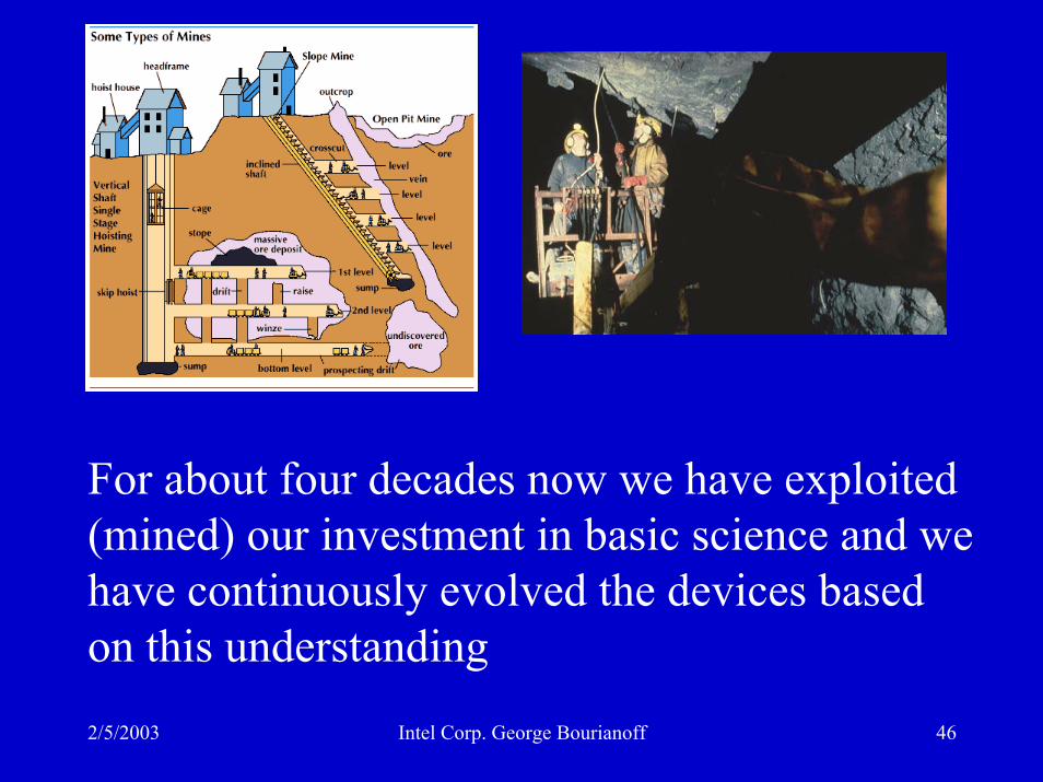
For about four decades now we have exploited (mined) our investment in basic science and we have continuously evolved the devices based on this understanding

2/5/2003 Intel Corp. George Bourianoff 47
Leakage is the limiter to SiO2 scalingIntegration is the key challenge to High K
Leakage is the limiter to SiO2 scalingLeakage is the limiter to SiO2 scalingIntegration is the key challenge to High KIntegration is the key challenge to High K
Silicon substrateSilicon substrate
GateGate
3.0nm High3.0nm High--kk90nm process90nm process
1X1X1X1X
Experimental highExperimental high--kk1.6X1.6X
< 0.01X< 0.01XCapacitanceCapacitance
LeakageLeakage
Silicon substrateSilicon substrate
1.2nm SiO1.2nm SiO22
GateGate
Source: Intel
Transistor gate oxide thickness trend
1
10
100
1970 1980 1990 2000 2010 2020First year in production
Dim
ensi
on (n
m) SiO2
High KSi-O bond:0.16nm
Nanotechnology for Gate Dielectrics

2/5/2003 Intel Corp. George Bourianoff 48
What new basic science is needed?
• Spin manipulation, e.g. transport, storage, detection, creation, …
• Geometry related quantum effects, e.g. quantum wedge, parabolic wells, …
• Precise location of atoms e.g. coherent manipulation of entangled wavefunctions
Rs →r
P+ P+
B-
Si
Source Drain

2/5/2003 Intel Corp. George Bourianoff 49
Transport in Si-Ge Core-Shell Structures-2.5
-2.0
-1.5
-1.0
-0.5
0.0
I DS
(µA)
-4 -3 -2 -1 0VDS (V)
VGS= -1.1 V
-0.7
-0.9
-0.5
-0.3
0.0
S
DG Si
GeSiOx
1000
800
600
400
200
0
-I DS (n
A)
-1.0 0.0 1.0VGS (V)
0.01
0.1
1
10
100
1000
-IDS (nA)
VDS= -1 V
1300 nA/V
330 mV/dec
G
S D
500 nm

2/5/2003 Intel Corp. George Bourianoff 50
Coaxially-Gated Si-Ge-2.5
-2.0
-1.5
-1.0
-0.5
0.0
0.5
I DS(µ
A)
-1.5 -1.0 -0.5 0.0VSD (V)
O VGS
-1 VGS
-2 VGS
3.0
2.5
2.0
1.5
1.0
0.5
0.0
I DS (µ
A)
-2 -1 0 1 2VGS (V)
0.1
1
10
100
1000
IDS (nA)
1.5 µA/V
450 mV/dec.
+1 VDS
Si
GeSiOx
Ge
2/5/2003 Intel Corp. George Bourianoff 51
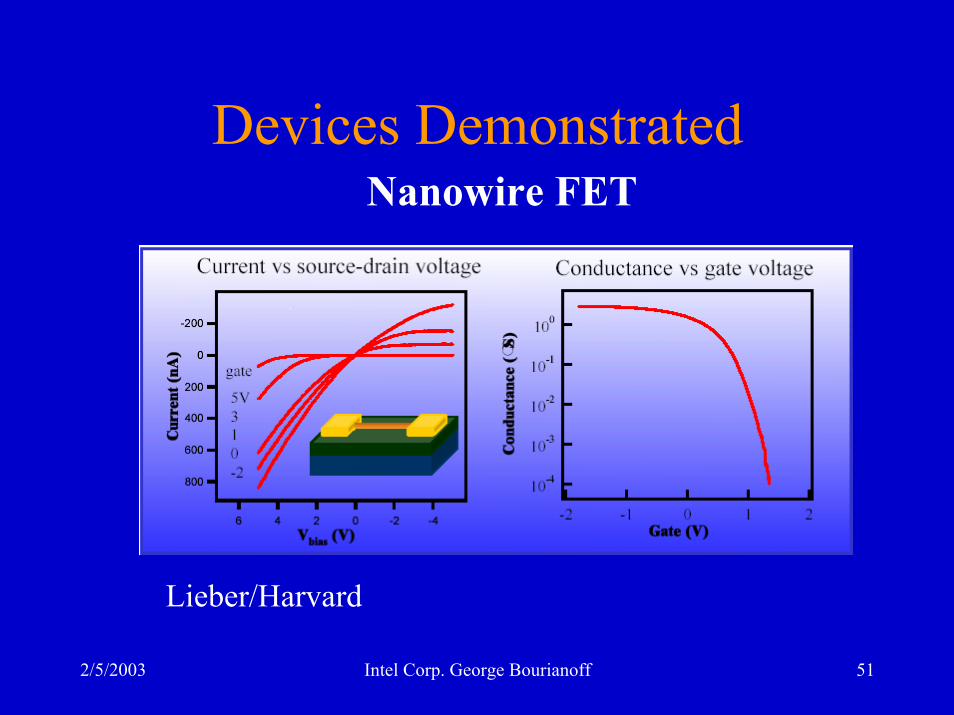
Devices DemonstratedNanowire FET
Lieber/Harvard
2/5/2003 Intel Corp. George Bourianoff 52
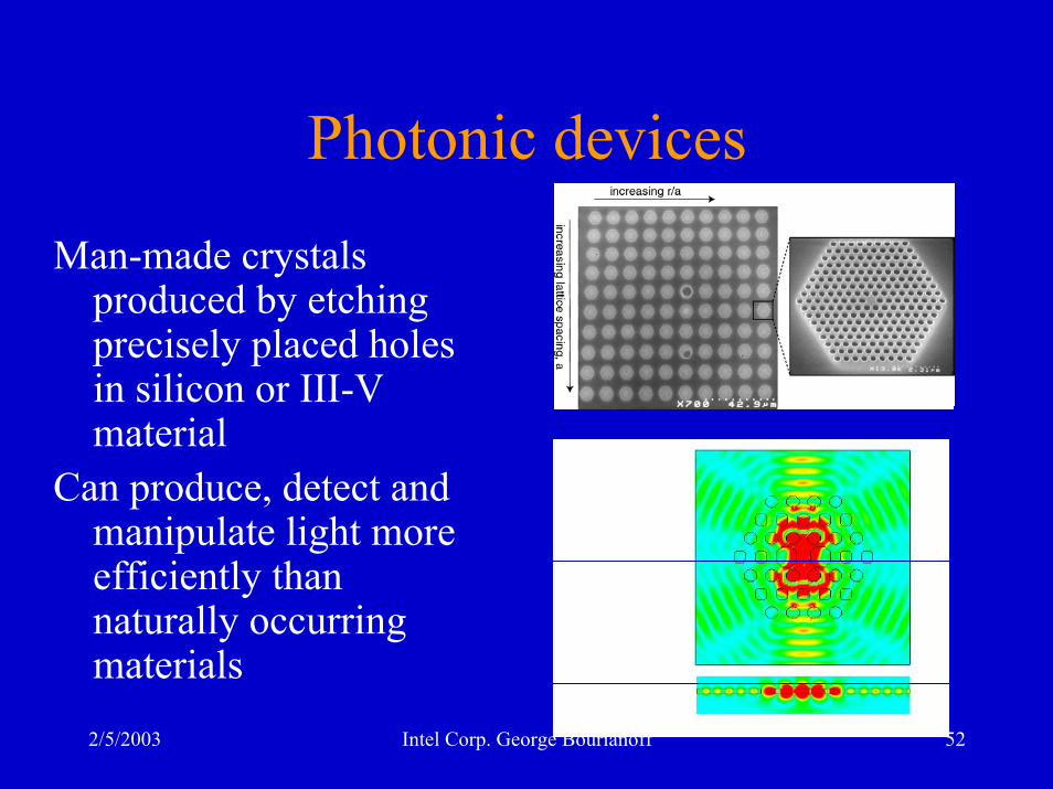
Photonic devices
Man-made crystals produced by etching precisely placed holes in silicon or III-V material
Can produce, detect and manipulate light more efficiently than naturally occurring materials

2/5/2003 Intel Corp. George Bourianoff 53
System software design needs to facilitate emerging technologies
Challenge• CMOS is based on Boolean logic and binary data
representation• Alternative technologies will require “native”
logic systems and data representations to optimize their performance
Solution?• Design science must provide functional
abstractions and interfaces to couple multiple, dissimilar technologies into a single functional system
2/5/2003 Intel Corp. George Bourianoff 54
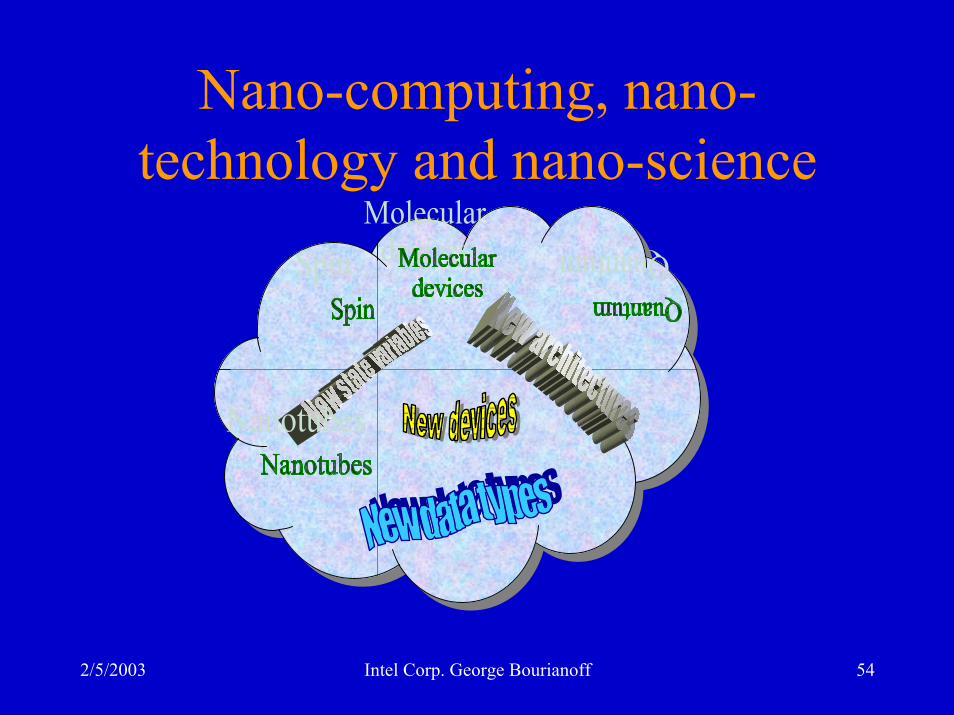
Nano-computing, nano-technology and nano-science

2/5/2003 Intel Corp. George Bourianoff 55
Changing architectural paradigmsCurrent
• Boolean logic• Binary data
representation
• 2D• Homogeneous• Globally interconnected• Synchronous• Von Neuman• 3 terminal
Future• Neural networks, CNN,
QCA,…• Associative, patterned,
memory based, … data representations
• 3D• Non homogeneous• Nearest neighbor• Asynchronous• Integrated memory/logic• 2 terminal