the fundamental technical knowledge of passive … ripple cu. polarity de-rating limitation re...
TRANSCRIPT

http://www.ty-top.com
The Fundamental Technical Knowledgeof Passive Components
for Windows version

-- Chapter 1Chapter 1--
CapacitorCapacitor

Impedance Characteristics of CapacitorImpedance Characteristics of Capacitor
Impedance equivalent circuit with capacitor is the same as the RLC series model.
ESR is constantIm
peda
nce
ESL increases
Impe
danc
e
Capacitance decreases
Impe
danc
e
Impe
danc
e
Frequency
Impe
danc
e
Frequency
Impe
danc
e
Frequency
ESR
ESL
Changes in Frequency Changes in ElementElements in Capacitor
Frequency
Frequency
Frequency
ESL: Decrease
ESR: Increase
Capacitance Cap. : Increase
What happens to the impedance level when connected in series?

Impedance Characteristics of CapacitorImpedance Characteristics of Capacitor
Impedance for series connection
0.001
0.01
0.1
1
10
100
0.001 0.01 0.1 1 10 100
周波数 [MHz]
インピーダンス
[Ω]
0.001
0.01
0.1
1
10
100
0.001 0.01 0.1 1 10 100
周波数 [MHz]
インピーダンス
[Ω]
Impedance depends on capacitance
Impedance depends on ESL
Resonance Point
Impedance depends on
ESR
Cap. : Increase
Resonance Point→Cap. : Increase,
ESL: IncreaseESR:
Decrease
ESL:Decrease
Impe
danc
e
FrequencyIm
peda
nce
Frequency
Impedance with different elements
Impedance characteristics varydepended on each element.
At resonance point, no impedance for Capacitor & ESL
(Impedance for ESR only) The frequency at resonance point depends
on Capacitor & ESL

Impedance Characteristics of CapacitorImpedance Characteristics of Capacitor
0.001
0.01
0.1
1
10
100
1 10 100 1000 10000 100000
周波数 [kHz]インピーダンス・ES
R
[Ω]
Ta 47μF ESRTa 47μF ZNEO 47μF ESRNEO 47μF ZSPCAP 47μF ESRSPCAP 47μF ZJM432BJ476MM ESRJM432BJ476MM ZSDK47μF ESRSDK47μF Z
MLCC47μF ESRMLCC47μF Z
Frequency characteristics for different type of capacitors
Frequency characteristic varies depended on the type of capacitor,
especially on ESR.
FrequencyIm
peda
nce
ESR varies depended on frequency
Impedance,ESR Freq.-Temperature Characteristic
0.001
0.01
0.1
1
10
100
1000
0.1 1 10 100 1000 10000 100000Frequency[KHz]
Impe
danc
e,ES
R[Ω
]
RZ
RLC varies depended on capacitors material, structure and case size
RLC Series Model→ ESR independent from frequency
ESR actually varies.
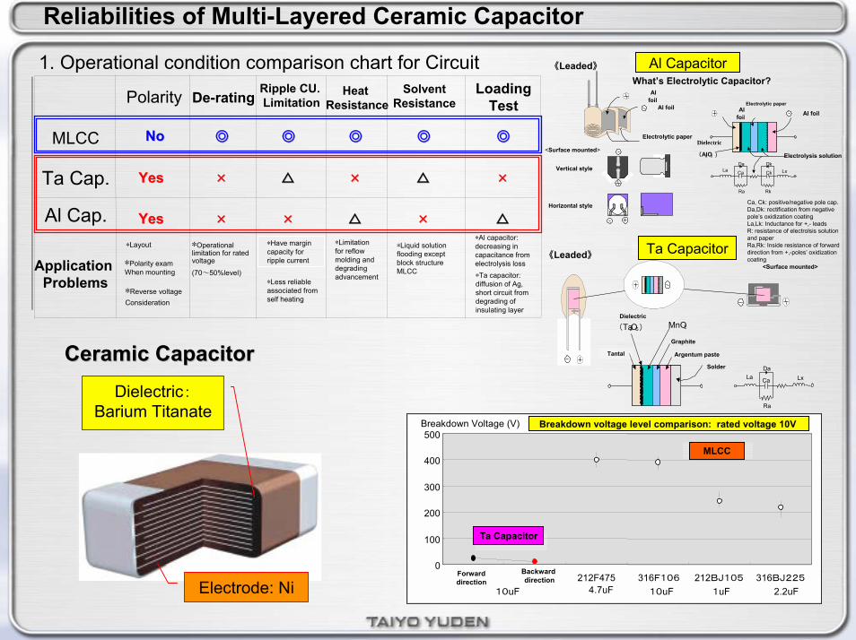
Reliabilities of Multi-Layered Ceramic Capacitor
1. Operational condition comparison chart for Circuit
《Leaded》
Da
Ra
CaLa Lx
(Ta2O5) MnO2
《Leaded》
Horizontal style
Vertical style
Alfoil
Alfoil
Al foilAl foil
(Al2O3 )Da Dk
Ra Rk
Ca Ck LxLa
Al CapacitorWhats Electrolytic Capacitor?
Electrolytic paper
Electrolytic paper
Dielectric
Electrolysis solution<Surface mounted>
Ta Capacitor<Surface mounted>
Dielectric
Tantal
Graphite
Argentum paste
Solder
Ca, Ck: positive/negative pole cap.Da,Dk: rectification from negative poles oxidization coatingLa,Lk: Inductance for +,- leadsR: resistance of electrolsis solutionand paperRa,Rk: Inside resistance of forwarddirection from +,-poles oxidization coating
NoNo
YesYes ×× ×× ××
YesYes ×× ×× ××
∗Operational limitation for rated voltage
(70~50%level)
MLCC
Ta Cap.
Al Cap.
Heatsistance
SolventResistance
Application Problems
∗Limitation for reflow molding and degrading advancement
∗Liquid solutionflooding except block structure MLCC
∗Al capacitor:decreasing in capacitance from electrolysis loss
LoadingTest
Ripple CU. Limitation RePolarity De-rating
∗Have margin capacity for ripple current
∗Layout
∗Polarity exam When mounting ∗Ta capacitor:
diffusion of Ag,short circuit fromdegrading of insulating layer
∗Less reliableassociated from self heating
∗Reverse voltageConsideration
Ceramic CapacitorCeramic Capacitor
0
100
200
300
400
500
212F475 316F106 212BJ105 316BJ22510uF 1uF 2.2uF10uF4.7uF
Breakdown Voltage (V)
Ta Capacitor
MLCC
Breakdown voltage level comparison: rated voltage 10V
Forwarddirection
Backward directionElectrode: Ni
Dielectric:Barium Titanate

Characteristics Comparison for the Different Type of Capacitors
Frequency Characteristics
0.001
0.01
0.1
1
10
100
1 10 100 1000 10000 100000
周波数 [kHz]
インピーダンス・ES
R
[Ω]
Ta 47μF ESRTa 47μF ZNEO 47μF ESRNEO 47μF ZSPCAP 47μF ESRSPCAP 47μF ZJM432BJ476MM ESRJM432BJ476MM ZSDK47μF ESRSDK47μF Z
MLCC47μF ESRMLCC47μF Z
ESR varies greatly depended on each type of capacitors.
Al>Ta>Functional Ta>Functional Al>ML
The lower ESR becomes, the lowerthe impedance for high frequency gets.
Al>Ta>Functional Ta>Functional Al>MLFrequency
Impe
danc
e
The most competitive merit
MLCC has superior frequency characteristics.

Characteristics Comparison for the Different Type of Capacitors
Ripple current characteristics for the different type of capacitorsRipple Current Characteristics
リップル電流対部品温度上昇の比較
0.1
1
10
100
0 0.5 1 1.5 2 2.5 3 3.5 4リップル電流(Arms)
積層コン47μF
タンタル47μF
POSCAP100μF
Temperature rise characteristic due to ripple current
Tem
pera
ture
rise
(deg
ree)
Ripple current(Arms)
MLCC47uF Tant.Cap47uFPOSCAP100uF
リップル電流対部品温度上昇の比較
0.1
1
10
100
0 0.5 1 1.5 2 2.5 3 3.5 4リップル電流(Arms)
積層コン47μF
タンタル47μF
POSCAP100μF
Temperature rise characteristic due to ripple current
Tem
pera
ture
rise
(deg
ree)
Ripple current(Arms)
MLCC47uF Tant.Cap47uFPOSCAP100uF
Given the same amount of calorific power,ripple current goes through MLCC the most because of its low ESR.
ESR ESL
CapacitorRipplecurrent Heat
Capacitor
Electrical energy is converted to heat when ripple current(AC) goes through capacitor.(DC does not go through it)
Heat shortens capacitors durability.
Heat
Electrical energy is converted to heatwhen current goes through resistance.
Operational recommendation of heat release value for MLCC is within 10.
There is no limitation of allowed ripple current for MLCC.
Operational recommendation of heat releasevalue for electrolytic capacitor is within 5.
Allowed ripple current is regulated by makers.

The Basic Knowledge of Circuits

The Functions of Bypass (decoupling) Capacitor
Impedance Low High
Noise effect of decreasing
More effective
Less effective
ICPower supply line
Noise + Load current Load Current
NoiseCurrent
To connect the noise current to the earth
(grounding)
The principle of operation for Bypass Capacitor
DC does not go through the capacitor (Impedance:∞)
DC is supplied directly to ICAC (noise) does go through the capacitor
AC (noise) is grounded
Noise Suppression → Stabilize IC operation
The Role of Bypass Capacitor Necessary Characteristics for Bypass CapacitorIt has low impedance.
(low prevention of an electric current)
It electrifies an electric current well.
It efficiently grounds the noise current.
It effectively decreases the noise current.
Noise: more Noise: lessLow Impedance High Impedance

The Functions of Bypass (decoupling) Capacitor
Replacement of Ta capacitor by Bypass CapacitorSelection Criteria for Capacitor
インピーダンスの比較
0.001
0.01
0.1
1
10
100
10 100 1000 10000 100000
Frequency(kHz
Impe
dance(Ω)
タンタル10μF
タンタル47μF
LMK212F475ZG
LMK316F106ZL
LMK212BJ225KG
EMK325BJ106KN
Change product name
to MLCC + capacitance
When the frequency is over 10kHz, the impedance of MLCC is lower than
that of Ta capacitor.
Impedance Comparison
Ta10uFTa47uF
Impedance,ESR Freq.-Temperature Characteristic
0.001
0.01
0.1
1
10
100
1000
0.1 1 10 100 1000 10000 100000Frequency[KHz]
Impe
danc
e,ES
R[Ω
]
RZ
Increasing in noise suppression effectiveness
Decreasing in noise suppression effectiveness
Maximum level for noise suppression effectiveness
Effectiveness of reduction in high frequency noise for MLCC is more superior than that of Ta capacitor.
Several kinds of Noise Frequencies
It enables to replace Ta capacitorwith a smaller value of MLCC.
Select a Capacitor based on noise frequency needs to be eliminated

The Functions of Backup Capacitor
IC IC IC IC
IC
Load current to ICLoad current doesnt stay constant.
Load current:small
Load current:large
Operating at low-speed
Operating at high-speed
High-speed load change
When ICs operational speed changes rapidly,large load current is quickly needed.
Low-speedoperation
High-speed operation
Time
Load
cur
rent
Power line for high-speed load changing Large load current is
quickly needed.The current cant flow to IC quickly enough.
Line voltage
Line voltage
Line voltage cant be maintained, thereforevoltage is dropped.
Voltage dropped
Line voltage
Line voltage decreases below the required operational voltage for IC.
The IC stops its operation.
Minimum required
operational voltage
for IC
Low-speedoperation
High-speedoperation
Time
Circ
uit v
olta
ge,
Load
cur
rent

The Functions of Backup Capacitor
IC ICESR
Electric current delays Making up for electriccurrent shortage
Voltage dropped
Line voltage
Maintaining Line
voltage
Low-speed operation
High-speedoperation
Minimum required operational voltage
for IC
Time
Line
vol
tage
,ne
eded
load
cur
rent
,D
isch
arge
cur
rent
from
C
apac
itor
Keeping the minimum required operational voltage for IC
Maintaining stable operation
Capacitors actual (considering equivalent circuit)
∗This is a simplified version, so disregard ESL
Capacitor
Voltage dropped by electric current
Voltage dropped by discharge
current
Line voltage dropped
Voltage dropped by ESR
Voltage dropped by electric discharge
Voltage risen by capacitor charging
Voltage risen by ESRLi
ne v
olta
ge
Capacitor and ESR decide the amount of voltage dropped
The Role of Backup Capacitor
Voltage fluctuation occurs when capacitor charging

The Functions of Backup Capacitor
ESRの比較
0.001
0.01
0.1
1
10
0.1 1 10 100 1000 10000 100000
周波数(KHz)
ESR(Ω)
積層コン22μF
タンタル100μF
Experimental result for Capacitance and ESR
タンタル100μFのリップル電圧
1μS/Div
20m
V/
Div
LMK432BJ226MMのリップル電圧
1μS/Div
20m
V/
Div
容量による電圧変動
ESRによる電圧変動
Experimentalcircuit
To oscilloscope
Power Supply
Voltage=5V
R = 1Ω
Current probe
RatingCapacitor
2SK2684
Loadresistance
R=5Ω
Pulse generator1945 (NF)
MLCC47µF∗7
Switching frequency =1000KHz
ESR comparison
High Value Low ESR
The fluctuation band of line becomes narrower.
Ripple Voltage of LMK432BJ226MM Ripple Voltage of 100uF Ta Cap
Voltage fluctuation by ESR
Voltage fluctuation by capacitance
MLCC 22uFTa Cap 100uF
Frequency (KHz)
Merits of MLCC
It enables to replace Ta capacitor with a smaller value of MLCC.
The effectiveness of MLCCs voltage fluctuation depressing effect is greater than that of Ta capacitor.

Application Examples for Backup Capacitor
100uF22uF10uF 47uFLMK325BJ106MN(積層コンデンサ10μF)
2.5μS/Div
50m
V/
Div
LMK432BJ226MM(積層コンデンサ22μF)
2.5μS/Div
50m
V/
Div
JMK432BJ476MM(積層コンデンサ47μF)
2.5μS/Div
50m
V/
Div
JMK550BJ107MM(積層コンデンサ100μF)
2.5μS/Div
50m
V/
Div
タンタルコンデンサ10μF
2.5μS/Div
50m
V/
Div
タンタルコンデンサ22μF
2.5μS/Div
50m
V/
Div
タンタルコンデンサ47μF
2.5μS/Div
50m
V/
Div
タンタルコンデンサ100μF
2.5μS/Div
50m
V/
Div
OSコン10μF
2.5μS/Div
50m
V/
Div
OSコン22μF
2.5μS/Div
50m
V/
Div
OSコン47μF
2.5μS/Div
50m
V/
Div
OSコン100μF
2.5μS/Div
50m
V/
Div
JMK316BJ106ML(10uF) JMK325BJ226MM(22uF) JMK432BJ476MM(47uF) JMK550BJ107MM(100uF)
OS-CON 10uF OS-CON 22uF OS-CON 47uF OS-CON 100uF
MLCCMLCC
Ta CapTa Cap
OSOS--CONCON
Ta Cap 10uF Ta Cap 22uF Ta Cap 47uF Ta Cap 100uF

The Basic Knowledge of Power The Basic Knowledge of Power Supply CircuitSupply Circuit

Series Regulator (3 Terminal Regulator)Series Regulator (3 Terminal Regulator)
Load current fluctuationCircuit operation (water gate model)
Load current
Controlling element (transistor)
Load current
Controlling element (transistor)
Inpu
t vo
ltage
Inpu
t vo
ltage
Out
put
volta
ge
Out
put
volta
ge
Controlling water gate to keep the water level constant
Producing output voltage by lowering certain amount of input
voltage
Controlling load current with transistor
Output voltage stays constant.
Step-down power supply

Series Regulator (3 Terminal Regulator)Series Regulator (3 Terminal Regulator)
Circuit structure Effects of input capacitorInput voltage > Output voltage Add alternate current to input voltage
purposely to measure input current amount with or without input capacitorRegulator
IC
Input Capacitor
-2000
-1000
0
1000
2000
-1 0 1
-2000
-1000
0
1000
2000
-1 0 1
With capacitors (MLCC)Without capacitors
Inpu
t Vol
tage
Vin
Vertical: mV Horizontal: u sec
IC IC
Input voltage is stabilized asinput capacitor is connected.
Output CapacitorConsisting of IC, input and output capacitors.
Noise + Load currentLoad current
IC
Function of input capacitor
Noise current
Connecting the line noise to the ground.
Same as the function of Bypass Capacitor

Series Regulator (3 Terminal Regulator)Series Regulator (3 Terminal Regulator)
IC Keeping line voltage
ICLine
voltage
Voltage dropped
Unable to supply current immediately
Load
Cur
rent
Iou
t
0
50
100
150
200
-10 -5 0 5 10
Measuring the voltage fluctuation when load change is occurred with/without output capacitor.
With capacitors (MLCC)Without capacitors
Out
put f
luct
uatio
n Δ
Vout
-2000
-1000
0
1000
-2 -1 0 1 2-2000
-1000
0
1000
-10 -5 0 5 10
ICIC
Effects of output capacitorFunction of output capacitor
Cover the current shortage
Supply current to control voltagefluctuation for rapid load change
Same as the function of Backup Capacitor Output voltage is stabilized as output
capacitor is connected.

StepStep--Down ConverterDown Converter
Transistor for switching power supply has only ON or OFF signal.
Switching operation
Controlling output voltage by switching
Circuit operation (water gate model)
Producing output voltage by lowering input voltage with transistor
Inpu
t vo
ltage
Out
put
volta
ge
Controlling element (transistor) Turn-on cycle Constant
Time to be ON ChangesPWM method
Turn-on cycle Changes
Time to be ON ConstantPFM method
Load current
Turn-on cycle of the switch Switching frequencyControlling element (transistor)
Out
put
volta
geInpu
t vo
ltage Control
ON ON ON
TimePWM
ON ONON
Control
Load current
TimePFM

StepStep--Down ConverterDown Converter
Circuit structure
Input capacitor
Control IC
Output capacitor
Choke coil
FET(2)
FET1
FET2
FET1
ON
FET1
ON
FET1
ON
Inpu
t cu
rren
t
Time
Large amount of alternating current (ripple current) flows.
Operation of input capacitorRipple current Ripple current flows
into input capacitor.
Heat generated by ESR
High tolerance for ripple current
Example: Permissible ripple current of a capacitor is 1A.
1A 1A1A1A 1A 1A
2A 2A2A
heatheat
Necessary characteristics of input capacitor
Input side currentRipple current: 6A
6 capacitors
ReducedExample: Permissible ripple current of a capacitor is 2A.
Ripple current: 6A
3 capacitors

Output side operation
ON ON ON
Time
Vo
lta
ge
Input voltage
Time
Output
capacitor
Choke coil
Input voltage is controlled
by an on-off switching.
It is smoothed with a
choke coil and an output
capacitor.
Points of output voltage to remember
Output
voltage
Ripple voltage is included.
Keeping higher voltage than the lowest operating
voltage of load IC.
Keep the band of
ripple voltage within
the rated value.
Ripple voltage
Rated output voltage
The lowest
operating voltage
Control voltage drop by
rapid load voltage
fluctuation
Rapid load voltage fluctuation
Rated output voltage
Step-Down ConverterStep-Down Converter
Vo
lta
ge
The lowest
operating voltage

StepStep--Down ConverterDown Converter
Repeating an on-off switching signal
Charge and discharge are repeated with output capacitor.
Voltage is fluctuated by current flowing in and out.
Ripple voltage
Operation at rapid load change
Same as Backup Capacitor
High Value MLCC
Suitable
ESR
CapacityCharging
Charging Current
Voltage rise
When charging
ESR
CapacityDischarging
Voltage drop
Discharging current
Voltage drop
When discharging
Repeat
Voltage rise
Factor for determining voltage drop by rapid load voltage fluctuation
Factor for determining ripple voltage
Necessary characteristics for capacitor when rapid load fluctuation occurred
High capacitanceSupply capacitor of high electronic charge
Low ESRReducing voltage drop when supplying
electronic charge
High capacitance and low ESRreduce ripple voltage.

Charge Pump (Boost)Charge Pump (Boost)
Lowering voltage fluctuation occurred by charging/discharging
Charging capacitor and output capacitor
Backup CapacitorSame as step-down output capacitor
Connecting charged capacitors
Output double amount of voltage than input
Smoothing with output capacitor (Switching)
Operation of charge pump (image)
V
Charging
V
C2
C1 Load2V
Output capacitor (smoothing capacitor)
Connect
Charging
Circuitry of charge pump (example: double boost)
Charging 2 capacitors separatelyIn
IC
Out
Input capacitor
Output capacitor
Capacitors for charging
C2C1V V
Required characteristics of capacitorV
V
High capacitance and low ESR are required.
Output voltage is determined by the number ofcapacitors connected. (integral multiple)

Comparison of Various Input CapacitorsComparison of Various Input CapacitorsSummary
各種コンデンサ周波数特性(1μF)
0.001
0.01
0.1
1
10
100
1000
10000
1 10 100 1000 10000 100000Freq. [kHz]
Z・ES
R
[Ω]
ML R
ML ZTa R
Ta Z
Al RAl Z
MLCC is excellent in noise suppression (low impedance).
Output fluctuation becomes smaller as IC input voltage stays constant.
Input fluctuation of 1Vrms Output fluctuation of 35Vrms
Vertical mV, Horizontal µsec
VsZZ
ZVin21
2+
=Δ (Z1:Line impedance)
Constant IC input voltage
Effect of noise suppression: large
Vs:1Vrms RegulatorICZ2
Z1
Vs ΔVin ΔVout7.5V
IC used:NJM78L05(JRC)Capacitor used:LMK212BJ105KG, Ta1uF, A11uF
コンデンサ未挿入
-2000
-1000
0
1000
2000
-1 0 1
入力変動 ΔVin
-100
-50
0
50
100
-1 0 1
出力変動 ΔVoutコンデンサ未挿入
-2000
-1000
0
1000
2000
-1 0 1
入力変動 ΔVin
-2000
-1000
0
1000
2000
-1 0 1
入力変動 ΔVin
-100
-50
0
50
100
-1 0 1
出力変動 ΔVout
-100
-50
0
50
100
-1 0 1
出力変動 ΔVout
入力コンデンサ挿入時の入力変動 ΔVin
-500
-250
0
250
500
-1 0 1
Al電解1μF
-500
-250
0
250
500
-1 0 1
積層1μF
-500
-250
0
250
500
-1 0 1
Ta電解1μF入力コンデンサ挿入時の入力変動 ΔVin
-500
-250
0
250
500
-1 0 1
Al電解1μF
-500
-250
0
250
500
-1 0 1
Al電解1μF
-500
-250
0
250
500
-1 0 1
積層1μF
-500
-250
0
250
500
-1 0 1
積層1μF
-500
-250
0
250
500
-1 0 1
Ta電解1μF
-500
-250
0
250
500
-1 0 1
Ta電解1μF
入力コンデンサ挿入時の出力変動 ΔVout
-20
-10
0
10
20
-1 0 1
Al電解1μF
-20
-10
0
10
20
-1 0 1
Ta電解1μF
-20
-10
0
10
20
-1 0 1
積層1μF入力コンデンサ挿入時の出力変動 ΔVout
-20
-10
0
10
20
-1 0 1
Al電解1μF
-20
-10
0
10
20
-1 0 1
Al電解1μF
-20
-10
0
10
20
-1 0 1
Ta電解1μF
-20
-10
0
10
20
-1 0 1
Ta電解1μF
-20
-10
0
10
20
-1 0 1
積層1μF
Vertical mV, Horizontal µsec
Vertical mV, Horizontal µsecFrequency Characteristics
Without CapacitorInput fluctuation
With Capacitor
With Capacitor
Al Cap Ta Cap MLCC
Al Cap Ta Cap MLCC
Output fluctuationMeasuring the noise absorption and the output voltage fluctuation by adding sine wave on input line
Input capacitor inserted
Capacitor (Z2) has low impedance.
MLCC has lower impedance than that of Ta for a wide range of frequency.MLCC is suitable for input capacitor.

Summary Operation Analysis of Output CapacitorOperation Analysis of Output Capacitor
Taコンと積層コンのESR-周波数特性比較
0.001
0.01
0.1
1
10
100
1000
1 10 100 1000 10000 100000Freq. [kHz]
ESR
[Ω]
JMK212BJ475KGTa4.7μF
IC used: R1112N331B (Ricoh)Input Cap: LMK212BJ225KG
Switching frequency: 100HzInput V: 5V
Load current: 150mA
ESR:Large ESR:Small
RegulatorIC
Iout
Vout
Using output capacitor with low ESRreduces the output voltage drop when load fluctuation occurred.
時間 μsec
0
50
100
150
200
-10 -5 0 5 10
負荷電流
Iout
mA
負荷電流波形
0
50
100
150
200
-10 -5 0 5 10
負荷電流
Iout
mA
0
50
100
150
200
-10 -5 0 5 10
負荷電流
Iout
mA
負荷電流波形
-4000
-2000
0
2000
-10 -5 0 5 10
未挿入Ta 4.7μFJMK212B475KG
時間 μsec
出力電圧変動 Δ
V
mV
出力電圧変動
-4000
-2000
0
2000
-10 -5 0 5 10
未挿入Ta 4.7μFJMK212B475KG
時間 μsec
出力電圧変動 Δ
V
mV
-4000
-2000
0
2000
-10 -5 0 5 10
未挿入Ta 4.7μFJMK212B475KG
時間 μsec
-4000
-2000
0
2000
-10 -5 0 5 10
未挿入Ta 4.7μFJMK212B475KG
時間 μsec
出力電圧変動 Δ
V
mV
出力電圧変動
ESRの変動分:大 ESRの変動分:小
-150
-100
-50
0
50
-10 -5 0 5 10
-150
-100
-50
0
50
-10 -5 0 5 10
Ta 4.7μF JMK212BJ475KG出力電圧変動 ΔV
Vertical mV, Horizontal µsec
Load Current Waveform Vout Fluctuation
Load
Cur
rent
Vout
Fluc
tuat
ion
Time Time
Vout Fluctuation
Frequency Characteristics Comparison Variable ESR: Large Variable ESR: Small
Without CapacitorTa 4.7uFJMK212B475KG
Observation of output voltage fluctuation
Waveform observation: Iout, Vout(Observing by the type of output capacitors)
MLCC with low ESR is well-suitable for output capacitor.

Development Method Direction for ML Lineups and ProposalsDevelopment Method Direction for ML Lineups and Proposals
Market demandCircuit segment Capacitor application segment Required performance
Digital circuit
Analog circuit
Amplifier
Arithmetic
Oscillation
Modem
DigitalPower supply
LogicHigh frequencyPower supply
Audio
Others
Decoupling
Backup
Smoothing
FilterCoupling
Focusing on impedance and ESR characteristics
Focusing on the stability of real capacitance, temperature and bias
High pressure
Time constant,Resonance
It is for circuit noise suppression and often used in digital circuits.
Low Impedance, Low ESRMLCC with Y5V characteristic and 0.1-10uF is best
suited
It may also be used for a circuit with large load change (CPU), stability of power line and
protection of IC.Low ESR, Low ESL, Low Impedance
MLCC with characteristics of Y5V,X5R,X7R and 0.1-10uF is best suited.
It is for in/output of power supply circuit and more used as the miniaturization of equipment.
Real capacitance, Low ESR, Low ESL, Low ImpedanceRated Voltage and Reliability
MLCC with characteristics of X5R, X7R and 1- tens of uF is best suited.
It is for amplifier, arithmetic, modem and filter circuits.
Stability of capacitance temperature and bias is important.
Temperature compensating dielectric type MLCC is best suited.
(CFCAP, TC type multilayer)

Proposal for Bypass CapacitorProposal for Bypass Capacitor
Replacement proposal for high capacitance Ta or Al electrolysis with ML 0.1uF
Common Case Example
Ta or Electrolysis Multilayer
0.1uF
High Value MLCC
Replaced only by a single High Value MLCC
Impedance for high frequency decreases.High frequency characteristic is advanced.
Replaced only by a single MLCC
0.001
0.01
0.1
1
10
100
1000
10000
1 10 100 1000 10000 100000
電解コン22μF+積層0.1μF電解コン22μF
積層0.1μF
電解コン22μF+積層0.1μFのインピーダンス特性
インピーダンス
[Ω]
周波数 [KHz]
0.001
0.01
0.1
1
10
100
1000
10000
1 10 100 1000 10000 100000
電解コン22μF+積層0.1μF電解コン22μF
積層0.1μF
電解コン22μF+積層0.1μFのインピーダンス特性
インピーダンス
[Ω]
周波数 [KHz]
0.001
0.01
0.1
1
10
100
1000
10000
1 10 100 1000 10000 100000
電解コン22μF+積層0.1μF
積層コンF特4.7μF
積層コンF特10μF
周波数 [KHz]
インピーダンス
[Ω]
大容量積層コンデンサのインピーダンス特性
0.001
0.01
0.1
1
10
100
1000
10000
1 10 100 1000 10000 100000
電解コン22μF+積層0.1μF
積層コンF特4.7μF
積層コンF特10μF
周波数 [KHz]
インピーダンス
[Ω]
大容量積層コンデンサのインピーダンス特性
Wider low impedance range compared with parallel use.
Impe
danc
e
Frequency
Impedance Characteristics
Impedance Characteristics
Impe
danc
e
Frequency
Electrolytic cap 22uF + MLCC 0.1uFElectrolytic cap 22uFMLCC 0.1uF
Electrolytic cap 22uF + MLCC 0.1uFMLCC 4.7uFMLCC 10uF

-- Chapter 2Chapter 2--
InductorInductor

Impedance of Inductor and Capacitor Inductive Reactance & Capacitive Reactance
Ohms law: (Alternate voltage)=(Impedance)×(Alternate current)
Impedance of pure inductor: inductive reactance: it increases as frequency increases.
周波数
インピーダンス
Inductance:High
Inductance:Medium
Inductance: Low
Impe
danc
e
Frequency
Alternatepower supply
Capacitance :C
Alternatepower supply
Inductance: LAccording to the Ohms law, the impedance of pure inductor isproportional to frequency and inductance.
V=L・di/dtSolving for V: V0=j2πf・L
Impedance is equal to:Z=XL=2πf・L
Frequency : fVoltage magnitude : VO
V=V0・exp(jωt)
Impedance of pure capacitor: capacitive reactance: it decreases as frequency decreases.
周波数
インピーダンス
Capacitance:LowCapacitance:
Medium
Capacitance:HighIm
peda
nce
Frequency
Frequency : fVoltage magnitude : VOV=V0・exp(jωt)
According to the Ohms law, the impedance of pure capacitor is inversely proportional to frequency and capacitance.
V=1/C・∫idtSolving for V: V0 = 1/(j2πf・C)
Impedance is equal to: Z = Xc = 1/(2πf・C)

Usage of Inductor and Capacitor: Low-pass Filter and High-pass Filter
Impedance of inductor: It increases as frequency increases.Impedance of capacitor: It decreases as frequency increases.
Typical characteristic of high-pass filter
IN OUT
GND
IN OUT
GND
周波数
Gain In case of low frequency,
inductors low Z: passing-through
capacitors high Z:passing-through instead
of dropping to the ground
In case of high frequency,inductors high Z:
blocked capacitors low Z:
dropping to the ground
Frequency
Gai
n
周波数
Gain
In case of low frequency,inductors low Z:
dropping to the groundcapacitors high Z:
blocked
In case of high frequency,inductors high Z:
passing-through instead of dropping to the ground
capacitors low Z:passing-through
Gai
n
Frequency
Typical characteristic of low-pass filter

Series Circuit・Series Resonance and Parallel Circuit・Parallel Resonance of Inductor and Capacitor
Impedance of inductor: It increases as frequency increases.Impedance of capacitor: It decreases as frequency increases.
Series circuit of pure inductor and capacitor:
Series resonance
Parallel circuit of pure Inductor and capacitor:
Parallel resonance
周波数
インピーダンス
周波数
インピーダンス
Capacitorimpedance
Inductors impedance
Impedance of series circuit
At resonant frequency:
zero
Capacitors impedance
Inductors impedance
Impedance of parallel circuit
At resonant frequency:
∞
Impe
danc
e
Frequency
Impe
danc
e
Frequency
Parallel circuit:Basically an electric
current flows in lower impedance.
Series circuit:Basically addition

Application of Inductor and Capacitor Application of Inductor and Capacitor BandBand--pass Filter and Trap Filterpass Filter and Trap Filter
Impedance of series circuit: Lowest at frequency resonance pointImpedance of parallel circuit: Highest at frequency resonance point
Typical characteristic of trap filter
Typical characteristic ofband-pass filter
OUTOUT IN
周波数
Gain
Parallel circuit:high Z at resonant
frequency:passing-through
instead of dropping to the ground
Frequency
IN
GNDGND
Series circuit: low Z at resonant
frequency:dropping to the
ground
周波数
Gain
Frequency

Real Characteristics of Inductor Self-Resonance Point Characteristic
Typical impedance characteristic of existing inductor
~similar to the typical impedance characteristic of LCR parallel circuit~
Multilayer inductor
周波数
インピーダンス
Impe
danc
eFrequency
Ex) Stray capacitanceexisted between internal and external electrode
Wound chip inductor
Ex) Stray capacitanceexisted between winding
wiresInductor for the low frequency side,
capacitor for the high frequency side and at resonance point, impedance is limited.

Application Ex. using Self-Resonance Characteristic of Inductor Trapping Formulation by Low-pass Filter
周波数
インピーダンス
周波数
インピーダンス
It has a sharp peak point at a resonance frequency.
Same inductance as inductor A, but its impedance is lower than
that of As.
Inductor A: impedance characteristic Inductor B: impedance characteristic
Impe
danc
e
Frequency
Impe
danc
e
Frequency
Example of Low-pass filter
OUTIN
GND
周波数
Gain
周波数
Gain
Trapping resulted from
the sharp peak point
Filter characteristic of pure inductor Inductor A in use
Frequency Frequency 周波数
Gain
Trap-less
Transmitting characteristic
deformed
Inductor B in use
Frequency
This self-resonance characteristic is proactively implemented for a filter circuit application, and therefore this unique characteristic needs to be considered
for both replacement and downsizing applications.

Real Characteristics of Inductor Lost Elements and Q Characteristic
Inductors Q factorML inductor Wound chip inductorImpedance of pure inductor:
Inductive reactance
Resistance elements
(Summation of loss)
R XL
Core materials:Hysterisis loss, Eddy current loss, dielectric material loss and more Internal electrode:DCR, resistance loss in high frequency zone originated from skin effect and morePure inductor has no loss at all.
Q factor is an approximation value which expresses how close an inductor is to be a pure inductor.The larger the Q factor an inductor has, the purer the inductor becomes on circuit.
Print internal electrode on sheet made of core
material
Inductive reactanceWind up wire around core Q =
Resistance elements
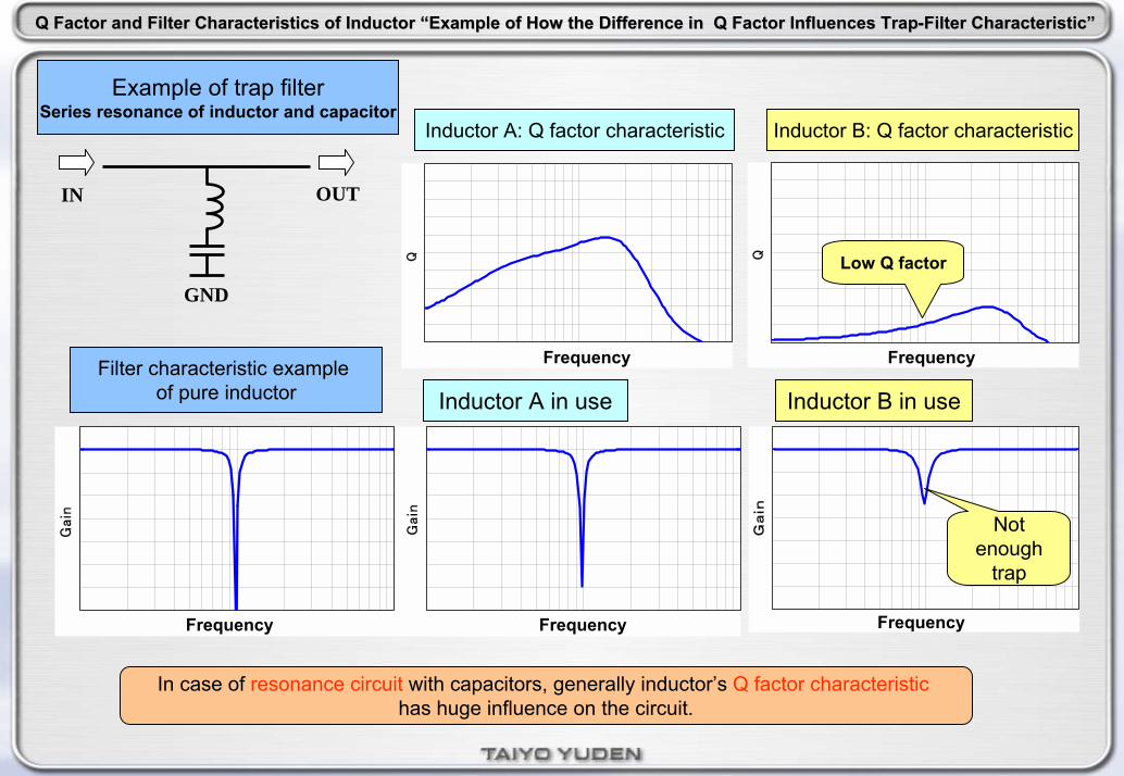
Q Factor and Filter Characteristics of Inductor Q Factor and Filter Characteristics of Inductor Example of How the Difference in Q Factor Influences TrapExample of How the Difference in Q Factor Influences Trap--Filter CharacteristicFilter Characteristic
周波数
Gain
周波数
Q
周波数
Q Low Q factor
Not enough
trap
周波数
Gain
周波数
Gain
Example of trap filterSeries resonance of inductor and capacitor
Filter characteristic example of pure inductor
Inductor A: Q factor characteristic
Inductor A in use
Inductor B: Q factor characteristic
Frequency
Frequency
Frequency
Frequency Frequency
OUTIN
GND
Inductor B in use
In case of resonance circuit with capacitors, generally inductors Q factor characteristichas huge influence on the circuit.
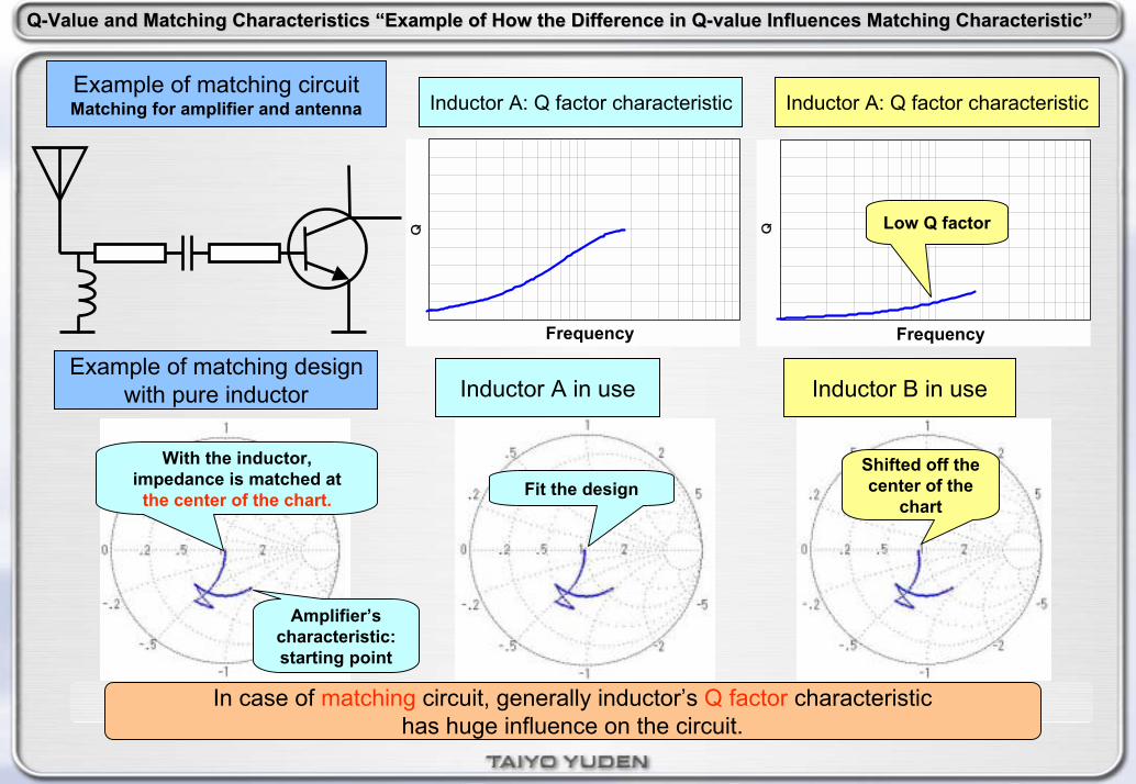
QQ--Value and Matching Characteristics Value and Matching Characteristics Example of How the Difference in QExample of How the Difference in Q--value Influences Matching Characteristicvalue Influences Matching Characteristic
Example of matching circuitMatching for amplifier and antenna
周波数
Q
Inductor A: Q factor characteristic
Frequency 周波数
Q Low Q factor
Inductor A: Q factor characteristic
Frequency
Shifted off the center of the
chart
With the inductor, impedance is matched at the center of the chart. Fit the design
Amplifiers characteristic:starting point
In case of matching circuit, generally inductors Q factor characteristichas huge influence on the circuit.
Example of matching designwith pure inductor Inductor A in use Inductor B in use

Coffee Break Q Factor of Inductor and Tan δof Capacitor
Impedance of pure inductor:inductive reactance
Resistance elements
(summation of loss)
XLR
=Q Resistance elements
Inductive reactance
Q factor of inductorinductors loss elements
Q factor is an approximation value which expresses how close an inductor is to be a pure inductor.
The larger the Q factor an inductor has, the purer the inductor becomes on circuit.
Impedance of pure capacitor:Capacitance reactance
Resistance elements
(summation of loss)
XcR
=Tan δResistance elements
Capacitance reactance
Tan δof capacitorcapacitors loss elements
Tan δ is a value which explains how fara capacitor is from being a pure capacitor.
The smaller the tan δ a capacitor has, the purer the capacitor becomes on circuit.

Real Characteristics of Inductor Example of DC Bias Characteristic
Example of impedance characteristicExample of inductorsDC bias characteristic
バイアス電流
インダクタンス
周波数
インピーダンス
周波数
インピーダンス
Example of an inductorwhich has a strong
characteristic against DC bias
Example of an inductor which has a weak
characteristicagainst DC bias
Impedance gets lowered as inductance is dropped by magneticsaturation.
An inductor which has a strong characteristic against DC biascan maintain high impedance level(vice versa).
Generally, an inductor is selected based on a margin level for both required inductance and impedance under operational circumstances.
Impe
danc
e
DC Bias Current
Impe
danc
eIm
peda
nce
Frequency
Frequency
In case of magnetic-material core which has the magnetic saturation characteristic, inductance is lowered by increasing in DC bias current.

Example of the Influence on InductorExample of the Influence on Inductors DC Bias Characteristic in use of Power Supply Chokes DC Bias Characteristic in use of Power Supply Choke
IC
周波数
インピーダンス
周波数
インピーダンス
A strongcharacteristic against DC bias and maintain high impedance
A weak characteristic against DC bias and unable to keep high impedance
Improved bypass characteristic at high frequency range Inferior bypass
characteristic
ON/OFF noise Load
fluctuation
Capacitor: Bypass tothe ground
Impedance increased by
high frequency
Inductor: Blocked by impedance
Bypass improved
Bypass characteristic of capacitor only
Inductor A: Impedance characteristic
Inductor A in use Inductor B in useIm
peda
nce
Frequency
Impe
danc
e
Frequency
Example of power supply choke circuitInductor B: Impedance characteristic
In case of power supply choke application, it should take full advantage of impedance characteristicin terms of designing of bypass circuit. Since impedance characteristic is degraded by DC bias,
it should be paid attention to see if the required value left under operational circumstances comparing with self-resonance characteristic.

Example of the Influence on InductorExample of the Influence on Inductor’’s DC Bias Characteristic of Power Supply Switching Circuit Applis DC Bias Characteristic of Power Supply Switching Circuit Applicationcation
バイアス電流
インダクタンス
IsVs
時間
Is 及び
Vs
Vs:ON ONOFF OFF ON
Is
Is increases as times goes on. Is increases even faster with
small inductance.
時間ICを流れる電流:Is
Switching ICbroken down
Example of step-up power supply circuitInductance: L
DC InputVin
DC OutputVout
While Vs turned on, Is flows to IC and then voltage is raised by inductor. When Vs being off, it is added
onto the input DC and then Output DC is up-converted.
When Vs is being on, Vin = L・dIs/dt, solving for this→Is = Vin / L・t
Is gradually increases as Vs turned on, it increases rapidly with small inductance .
It is important to know of the tolerance currentwhen selecting an inductor for the power supply circuit.
General relationship between DC bias characteristic and Is
As DC bias current increases, the
inductance starts decreasing.
DC bias current passes at some
point, inductance drops suddenly.
When DC bias current passes
the tolerance current, (for the worst case
scenario) the switchingIC is broken down.
Switching interval is shortened by high frequency power supply IC, and therefore large inductance is
no longer needed for IC.Addition to this, flat DC bias characteristic isn’t ideal for all kinds of circuit. It would be better to match a specific DC bias characteristic with IC and power supply demand.
and
Time
Impe
danc
e
DC Bias current
Cur
rent
(Is)
flow
s in
to IC
Time

Coffee Break The Charging and Discharging Mechanisms of Capacitor
+Q
-Q
Electric current
Electric current
Apply voltage to a capacitor, electronic charge is built up in the inside of capacitor. On the other hand, when both sides of external electrodes are short-circuited, the capacitor discharges the built-up electronic charge.
The quantity of electronic charge is proportional to voltage. (In case with inductor, an electronic current creates magnetic flux. The quantity of magnetic flux is proportional toelectronic current.)
Capacitors capacitance is the constant of proportion between the quantity of electronic charge and voltage. (In case with inductor, inductance is the constant of proportion from magnetic flux and electronic current.
A time-varying electric charge or discharge induces electric current.In case with inductor, a time-varying magnetic flux induces electric voltage.
Charging mechanism
Increasing electric charge
Voltage raisedBatteryCapacitor
Discharging mechanism
+QDecreasing electric charge
Voltage dropped -Q Capacitor
A time-varying electric charge induces electric current.-I = dQ/dt
Capacitance is the constant of proportion derived from the relationship between the quantity of electric
charge and voltage.Q = C・V
The relationship among voltage, electric current and capacitance
-V = 1/c・∫idt or I = C・dV/dtThe equivalent relationship for inductor
-V = L・di/dt

-- Chapter 3 Chapter 3 --
ElectroElectro--Magnetic CompatibilityMagnetic Compatibility(EMC)(EMC)

The Different Types of NoiseThe Different Types of Noise
Spark Gaps and Varistors.Beads and Resistors for low voltage.
Instantaneous high voltage and current. It is occurred by natural phenomenon (eg. thunderstorm), inserting and removing a cable, etc.
Surge noise
Mainly Chip Varistors and Diodes. Capacitors and Beads may also be used.
A discharge phenomenon, which is caused by friction charge. It causes element destruction and malfunctions.
Electrostatic
Mainly capacitorsA fluctuation by voltage drop occurred when IC operates. It becomes a problem at power line with high power consumption for CPU, etc.
Ripple voltage (current)
Mainly Surface Mount High Current Inductors NP series, Wound Chip Inductors LB series and such ferrite components and capacitors for DC-DC, etc.
It runs through DC power line, i.e. switching noise, etc. The sources are DC-DC power supply converter, etc.
Conduction noise (noise
terminal voltage)
Mainly ML Ferrite Chip Beads BK series, Rectangular Ferrite Chip Beads (High Current) FB series M type. Resistors and capacitors may also be used.
It leaks out as an electromagnetic wave. The sources are signal line and power line. There are restrictions in countries. (VCCI, FCC, CISPR, EN, etc.)
Radiation noise
Countermeasure componentsContents

Standards of Radiation Electric FieldStandards of Radiation Electric Field
U.S.A.: FCC part15
Europe: EN55022
Other countries: Setting regulation based on CISPR
Regulation of the frequency band is between 30MHz to 1000MHz for VCCI.
Others are referred on the next page.
Global Standard: CISPR
Japan: VCC class2(Consumer Equipment)

EMI Regulation Example for High Frequency Band (EMI Regulation Example for High Frequency Band (Tightening Regulation for GHz band noise)Tightening Regulation for GHz band noise)
1. CISPR 11 Group 2 Class B (1999 industry, chemistry, medical)
For equipment with embedded frequency of 400MHz and above
Regulated frequency: 1-2.4GHz band Standard: 70dBuV/m and below (3m electric field intensity)
2. CISPR 22 CIS/G/210/CD (2001 IT equipment)For equipment with embedded frequency of 200MHz and above
Regulated frequency: 1-2.7GHz band Standard: Average of 50dBuV/m and below,
Max 70dBuV/m and below (3m electric field intensity)
3. FCC Part 15 (IT equipment) Measurement up to 2GHz is required for an operation between 108 to 500MHz band.
Measurement up to 5GHz is required for an operation between 500 to 1000MHz band.

Mechanism of Radiation Noise 1Mechanism of Radiation Noise 1
SpectrumDigital waveform
Measurement system: Spectrum AnalyzerMeasurement system: Oscilloscope
Time
Voltage (current)
Frequency
Spectrum Analyzer
Oscillo
scop
e
Frequency
Noise
(voltage, current)
Fourier transform
Time axis is transformed to frequency.
Noise standard restricts the noise received with an antenna.
Digital wave is formed by various frequencies.
Voltage (current)
Time

Mechanism of Radiation Noise 2Mechanism of Radiation Noise 2
Electric and magnetic fields occur with alternate current.
Current Magnetic field
Electric field
0V
Voltage
0A
Current
Electric field
Magnetic fieldFlux occurs only with direct current.
Current Flux
0V
voltage current
0A
Noise Clock
Radiated from digital wave
・・・
IC
NoiseDigital signal
IC
VccVcc
Leakage of high frequency
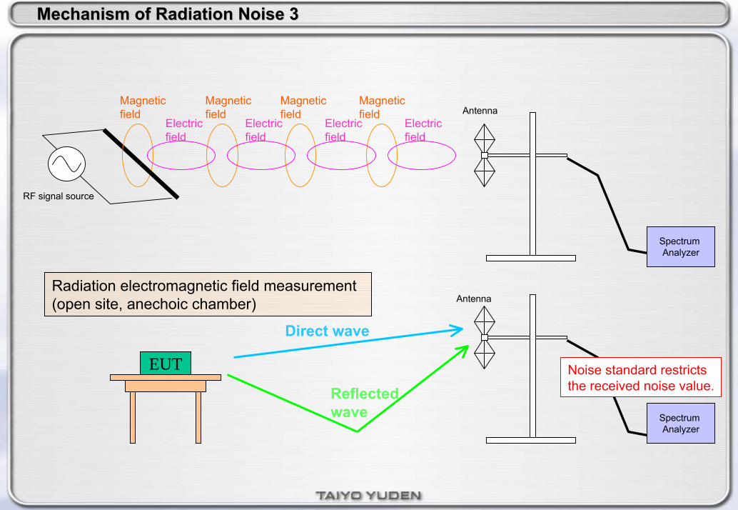
Mechanism of Radiation Noise 3Mechanism of Radiation Noise 3
Magnetic field
Electric field
Electric field
Spectrum Analyzer
RF signal source
AntennaMagnetic field
Magnetic field
Magnetic field
Electric field
Electric field
EUT
Direct wave
Reflected wave Spectrum
Analyzer
Antenna
Noise standard restricts the received noise value.
Radiation electromagnetic field measurement (open site, anechoic chamber)

Mechanism of Radiation Noise 4Mechanism of Radiation Noise 4
Time
Voltage
Frequency
Noise
Spectrum changes with waveform distortion.
Ringing occurring
Voltage
Time
FrequencyN
oise
Level changes
Cause: mismatching of transmission line
Standing wave
=traveling wave+reflected wave Because harmonics of a digital signal make a standing wave, the emission of the signal increases as noise.Reflected wave
Traveling wave
Transmission line pattern Mismatching of impedance

Fin.
http://www.ty-top.com