the development system and circuit design of buck …
TRANSCRIPT

THE DEVELOPMENT SYSTEM AND CIRCUIT
DESIGN OF BUCK BOOST CONVERTER FOR PV
SOLAR SYSTEM
NURSHUHADAH BINTI ZAHARUDIN
BACHELOR OF ENGINEERING TECHNOLOGY
(ELECTRICAL) WITH HONS

ii
UNIVERSITI MALAYSIA PAHANG
BUCK BOOST CONVERTER FOR PV SOLAR SYSTEM
NURSHUHADAH BINTI ZAHARUDIN
Thesis submitted in fulfilment of the requirements
for the award of the degree of
Bachelor of Engineering Technology in Electrical
Faculty of Engineering Technology
UNIVERSITI MALAYSIA PAHANG
JANUARY 2018

v
STATEMENT OF AWARD FOR DEGREE
1. Bachelor of Engineering Technology
Thesis submitted in fulfilmentof the requirements for the award of the degree of
Bachelor of Engineering Technology in Electrical.

vi
SUPERVISOR’S DECLARATION
We hereby declare that we have checked this thesis and in our opinion, this thesis is
adequate in terms of scope and quality for the award of degree of Bachelor of
Engineering Technology in Electrical.
Signature:
Name of Supervisor: DR WAHEB ABDUL JABAR
Position: LECTURER, FACULTY OF ENGINEERING TECHNOLOGY,
UNIVERSITI MALAYSIA PAHANG.
Date: JANUARY 2018

vii
STUDENT’S DECLARATION
I hereby declare that the work in this thesis is my own except for quotations and
summaries in which have been duly acknowledged. The thesis has not been accepted for
any degree and is not concurrently submitted for award of other degree.
Signature:
Name: NURSHUHADAH BINTI ZAHARUDIN
ID Number: TB14007
Date: JANUARY 2018

viii
ACKNOWLEDGEMENTS
In the name of Allah, the Most Merciful and The Gracious. Praise be to Allah,
finally this thesis reaches the end with the support of many individuals.
Here I would like to extend my sincere gratitude to all of them. First and foremost
I want to thank my supervisor, Dr Waheb Abdul Jabar and my co-supervisor Dr.Yasir
H.Naif for his guidance, continuous support and encouragement, endless patience, and
also for being very understanding supervisor. He has always impressed me with his
intelligence and knowledge. He also a very generous person as he always shared anything
that he knew that can help me in this project. I really appreciate his kindness in spent a
lot of his time together to finish this project and for correcting my mistakes while
completing this thesis. I’ve learned a lot since the beginning of this project until the
project is succesfully done.
Many specials thanks goes to all the instructors from Faculty of Engineering
Technology (FTEK) who have gave me support and guidance especially in doing
mechanical part for this project.
I acknowledge my sincere gratitude to my strong backbone support which is my
beloved parents Encik.Zaharudin Bin Murad and Puan Maimon Binti Zakaria, also my
others family members for their love and sacrifice throughout my life. They are the place
where I went to when facing some emotional issues while doing this project. I also thank
them for all the financial support that they gave me during my studies.
Lastly, thanks to my friends who always support me and be there for me during
ups and downs in my life. Without all of them that I had mention above, I would not be
where I be today. Thank you and may Allah shower all of us with his blessings.

xi
TABLE OF CONTENTS
Page
SUPERVISOR’S DECLARATION v
STUDENT’S DECLARATION vi
ACKNOWLEDGEMENT vii
ABSTRACT viii
TABLE OF CONTENTS xi
LIST OF TABLES xiii
LIST OF FIGURES xiv
LIST OF SYMBOLS xv
LIST OF ABBREVIATION xvi
CHAPTER 1 INTRODUCTION
CHAPTER 2 LITERATURE REVIEW
1.1 Project Background…………………………………… 1
1.2 Objective………………………………………………. 2
1.3 Problem statement……………………………………... 3
1.4 Scope Project…………………………………………... 4
2.1 Introduction...………………………………………….. 4
2.2 PV Solar System…………………………………......… 6
2.3 Sensitive load toward Regulated Voltage...…………... 13
2.4 Buck Boost Converter…………………………………. 14
2.4.1 DC – DC Converter……………………………......… 14
2.4.2 Buck Converter…………………………...…………... 16
2.4.3 Boost Converter…………………………………. 19
2.4.4 Buck Boost Converter…………………………......… 20
2.5 Mosfet …………………………………...…………... 23
2.6 Capacitor…………………………………. 24
2.7 Inductor…………………………………......… 25

xii
CHAPTER 3 METHODOLOGY
CHAPTER 4 RESULT AND DISCUSSION
CHAPTER 5 CONCLUSION AND RECOMMENDATION
REFERENCES.………………………………………………………….. 47
APPENDICES…………………………………………………………… 50
2.8 Diode ………………………………........…………... 25
2.9 Arduino Atmega328…………………………………. 25
2.10 Battery…………….…………………………………. 27
3.1 Introduction ……………………………..…............. 29
3.2 Flowchart of the process………………… 30
3.3 Designing of buck boost converter…………………. 33
3.4 Circuit Simulation using MULTISIM ………………. 33
3.5 PWM Generation using function generator………… 36
3.6 PWM Generation using arduino controller…………. 37
3.5 Buck Boost Converter circuit using proteus 7………
39
4.1 Simluation result and practical result………….............. 41
4.2 Buck mode reult ………………...........
4.3 Ideal mode result………………………………………
4.4 Boost mode result …………………………………
41
42
43
5.1 Conclusion……………………………........................... 46
5.2 Recommendation…………………………..................... 46

xiii
LIST OF TABLES
Table No. Title Page
3.1 The value of duty cycle at different value of voltage input 32
3.2 The value of every component 36

xiv
LIST OF FIGURES
Figure No. Title Page
2.1 Cut way of Monocrystalline Solar Panel
7
2.2 Diagram of Grid-connected PV solar system
8
2.3 Diagram of Direct-Coupled System 9
2.4 Diagram of stand alone PV system with battery storage
powering DC and AC load
10
2.5 Line Voltage 14
2.6 The system of DC-DC Converter 16
2.7 Buck DC-DC Converter circuit 17
2.8 Buck Converter Waveform 18
2.9 Boost DC-DC Converter circuit 19
2.10
2.11
2.12
2.13
Connection of buck-boost converter circuit
Graph of buck boost converter
Graph operation mode in buck boost converter
Capacitor’s C Voltage
19
21
22
23
2.14
Arduino Microcontroller
24
3.1
Flowchart shows the flow of the project development
system
31
3.2
Connection of buck boost converter using MULTISIM
35
3.3
Circuit configuration in MULTISIM
35
3.4
Flowchart of arduino PWM closed loop system
38
3.5 Proteus system Virtual Modelling 39
4.1 Simulation result for boost mode 41
4.2 Practical result for boost mode 42
4.3 Simulation result for ideal mode 42
4.4 Practical result for ideal mode 43

xv
4.5 Simulation result for buck mode 44
4,6 Practical result for buck mode 45
xvi
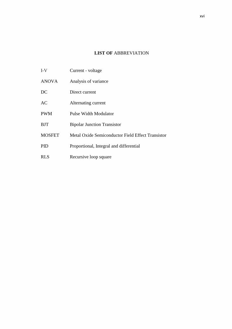
LIST OF ABBREVIATION
I-V Current - voltage
ANOVA Analysis of variance
DC Direct current
AC Alternating current
PWM Pulse Width Modulator
BJT Bipolar Junction Transistor
MOSFET Metal Oxide Semiconductor Field Effect Transistor
PID
RLS
Proportional, Integral and differential
Recursive loop square