the design for test architecture in digital section of the atlas fe-i4 chip vladimir zivkovic...
TRANSCRIPT

The Design for Test Architecture in Digital Section of the ATLAS FE-I4 Chip
Vladimir ZivkovicNational Institute for Subatomic Physics
(NIKHEF)Amsterdam, the Netherlands
Topical Workshop on Electronics for Particle Physics (TWEPP) 2010Aachen, September 22

2
Outline
• Introduction• Implementation of the Design-for-Test (DfT)
Architecture in FE-I4 • Test Development Flow• Method evaluation - benchmarking• Conclusion and further challenges
Vladimir Zivkovic 22/09/2010

Pixel array size 80x336
Pixel size 50x250 mm2
Maximum charge 100 000 e-
Hit trigger association resolution 25 ns
Same pixel two-hit discrimination (time) 400 ns
Tuned threshold dispersion < 100 e-
Charge resolution 4 bits
ADC method TOT
Radiation tolerance 250 MRad
Operating temperature range -40o C to 60o C
Average hit rate with < 1% data loss 400 MHz/cm2
Readout initiation Trigger command
Max number of consecutive triggers 16
Trigger latency (max) 6.4 s
Maximum sustained trigger rate 200 KHz
External clock input (nominal) 40 MHz
Single serial command input (nominal) 40 Mb/s
Single serial data output (nominal) 160 Mb/s
Output data encoding 8b/10b
I/O signals LVDS
FE-I4 ChipInsertable B-Layer (IBL) Application
Vladimir Zivkovic 3 22/09/2010

4
Importance of IC Test• IBL has raised concerns on large-volume product quality:
yield has to be increased• Complexity of State-of-the-Art ICs produced in deep
submicron technology requires dedicated approach for test
• Times when the designers were able to write the procedures to distinguish between correct and faulty chips quickly, with ease and map them to tester platforms, are past long times ago
Physical Defect: An on-chip flaw introduced during fabrication or packaging of an individual ASIC that makes the device malfunctioning
Transistor always ON
Short circuit
Open circuit
Oxide pinholes
22/09/2010Vladimir Zivkovic

5
Test development process in deep-submicron technologies
Rule of the game: Tester access to the Device Under Test (DUT) only possible through its primary I/O ports – the Design for Test (DfT) needed
Internal probing of ICs too costly
Fact: Test is not any longer back-end process – the development and implementation begins during the design stage
Test Development and Test Vector Generation
22/09/2010Vladimir Zivkovic
Test programme
------------ ----
--------------

6
Functional vs Structural Testing• Functional testing verifies that a circuit fulfils the desired spec• Functional testing not feasible for exhaustive tests
– An example: 32-bit adder requires 265 ≈ 3.7*1019 test vectors
• Structural test focuses rather on the circuit structure and can cover manufacturing defects that otherwise may not have been detected by functional testing– Power or ground shorts– Open interconnection on the die– Short-circuited drain or source of the transistor, caused by metal-spike
through
22/09/2010Vladimir Zivkovic

7
Outline
• Introduction• Implementation of the DfT Architecture in
FE-I4 • Test Development Flow• Method evaluation - benchmarking• Conclusion and further challenges
22/09/2010Vladimir Zivkovic

PLL
The DfT architectural choice: Full-scan Modular (Core-Based) test architecture
8Vladimir Zivkovic 22/09/2010
FE-I4 Architecture Overview
The Design for Test Circuitries are inserted in the output data path of the readout part of the FE-I4
For the sake of SEU robustness, the design makes extensive use of triple redundancy, emphasizing further the internal test structures requirement
Courtesy of M. Barbero*

9
Basics of digital structural testing
Most of the commercials Automatic Test Pattern Generator (ATPG) based on stuck-at fault model (D-algorithm)
• Stimulus and response calculated by Automatic Test Pattern Generator (ATPG) based on fault models
• Applied on the whole device or in a divide-and-conquer fashion, individually on the embedded modules (cores)
DUT
0110100010110001
:
0001011110100001
:
comparators fail flags
stimuli
response
Clk
logic logiclogic logic
Clk
Scan-in
Scan-out
Se
Stuck-at Fault Model: A logical model representing the effects of a physical defect
SA1 SA0
Handling sequential designs: full-scan concept
Access to internal terminals of the embedded modules (cores) through design for test (DfT) is necessary
22/09/2010Vladimir Zivkovic

10
Core-Based Test concept
Embedded module
source sink
1. Test Pattern Source and Sink
wrapper
3. Core Test Wrapper
coreTAM
2. Test Access Mechanism (TAM)
TAMTestRail TestRail
[ Zorian, Marinissen, Dey - ITC’98 ]
22/09/2010Vladimir Zivkovic

11
wrapper
Wrapper cells providing function access and test controllability + observability at IP’s data terminals
Core-Based Test in FE-I4
from/to other cores
from/to other cores from/to other cores
EOCHL DOB
wrapper
Pixel Array
IC-level FE-I4
MandatoryInternal scan chain insertion
si2
so2so1
si1
SEU proof
22/09/2010
TestRail access to wrapper cells (‘surround chains’) and IP flip flops (‘scan chains’)
IC-level Test Control & Data
Vladimir Zivkovic

12
Wrapper cells in the nutshellInput isolation Output isolation
0d _ in
s tc ks c ane n a b le
F Fs ca n_ in
s ca n_ o u t
IP inp u t
Test Shells c i
D
0
sco
d_outIP output
Test Shell
stck
scan enable
s c a n _ i n F F s c a n _ o u t
D
Note: Only the combinatorial inputs require isolation
Deglitcher cells implemented on scan enable, test mode and reset signals
&/||
Signal_inSignal_out
Delay 5ns
22/09/2010Vladimir Zivkovic
13
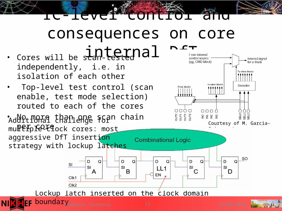
IC-level control and consequences on core internal DfT
• Cores will be scan-tested independently, i.e. in isolation of each other
• Top-level test control (scan enable, test mode selection) routed to each of the cores
• No more than one scan chain per core
Courtesy of M. Garcia-Sciveres *
Lockup latch inserted on the clock domain boundary
Additional challenge for multiple-clock cores: most aggressive DfT insertion strategy with lockup latches
22/09/2010Vladimir Zivkovic

14
Outline
• Introduction• Implementation of the DfT Architecture in
FE-I4 • Test Development Flow• Method evaluation - benchmarking• Conclusion and further challenges
22/09/2010Vladimir Zivkovic

15
DfT generation: Two-pass mapped flow
Scanablenetlist (.v)LibraryConstraints
after scan (.sdc)
Placement
Clock tree synthesis
Timing Analysis
Optimization postCTS
Routing/optimization
Add filler cells
Verification, DfM
Floorplan (Power bars, blockings)
Chip finishing in Virtuoso
VIRTUOSO
OPENACCESS
2.2
Scan Chain Reordering
Control, configuration, fp
Physical netlist (.v)Backannotation(MMMC, .SDF, .SPEF,)
Synopsys Design & DfTCompilerLibrary
Design & Test Constraints (.tcl)
Control Script(.tcl)
Input, output delay =5ns,Clock(s) timing and uncertainty (500p)False path on reset, scan, wire_load_model,
scx3_cmos8rf_lpvt_ff_1p32v_m55c.db scx3_cmos8rf_rvt_tt_1p2v_25c.db scx3_cmos8rf_rvt_ss_1p08v_70c.db
Design databaseRTL Netlist
(.v) (.sv)
Wrapper
functioninputs function
outputs
IP
TestRailinputs
TestRailoutputs
Scannable Netlist(.v)
Constraints after scan (.sdc)
Physical Implementation
Synthesis & DfT
Courtesy of MUG *
22/09/2010Vladimir Zivkovic

16
ATPG & Test Assembly• Generate the test patterns• Generate the test bench for the simulation with both stimuli and
response with timing and wave information• Assemble the test patterns of the IP(s) into the test vectors running at
the tester platform
22/09/2010Vladimir Zivkovic
WaveForm {
Pin = rzClocks;
Drive = RZ, t1, t2;
}
WaveForm {Pin = outputs;Expect = SB, t1, t2;
}
WaveForm {
Pin = inputs;
Drive = NR, tdel;
}
tdel
vector
waveform
tdel
t
period
t1
vector
waveform
t2
t
period
t1
vector
waveform
t2
t
period
t1 t2
Timing TetraMax
ATPG
STILvectors
test bench
NCsim
DfT
Protocols
test lib
Physical netlist
ATPG constraints

17
Test execution
DIB Integration
22/09/2010Vladimir Zivkovic
18
Outline
• Introduction• Implementation of the DfT Architecture in
FE-I4 • Test Development Flow• Method evaluation - benchmarking• Conclusion and further challenges
22/09/2010Vladimir Zivkovic

19
Reports• End of Chip Logic (EOCHL) Core
– Total faults 105980– Fault coverage 90.83%– Number of patterns 231 (3192 bit-stream wide,
each)– DfT area overhead 8 % relative, < 0.1% absolute
• Data Output Block (DOB) Core– Total faults 2183– Fault coverage 78.67%– Number of patterns 26
Test Cost (time) = i
Nc
iii
i
i
ftckpp
nsc
ff 11
1
22/09/2010Vladimir Zivkovic
Nc nr of modules
ff nr of flip-flops
nsc nr os scan-chains
p nr of patterns
ftck Test clock frequency

20
Simulation charts (EOCHL core)
Continuity pattern
Pattern1 Pattern2 …
22/09/2010Vladimir Zivkovic

21
Conclusion
• The test infrastructure in digital portion of ATLAS FEI4 IC is in place for production test
• The fault coverage figures are sufficiently high for this type of application
• Minimal area overhead, while the performance penalties are virtually none
• Reusability of the method• Compliant to the industrial standards
22/09/2010Vladimir Zivkovic

22
Future challenges• Implementing the DfT in a digital portion only may not be
sufficient – analog mixed-signal dedicated test approach needed
• Probability of the random defect landing on a random location leads to unpredictable quality levels
• Gaining in importance with smaller feature size
22/09/2010Vladimir Zivkovic

23
Future challenges (II)• Apply Analog Mixed-Signal DfT/BIST
– E.g. analog/mixed-signal test bus and/or digitally controlled patterns to test AMS block
• Automate the AMS Test Development (no analog ATPG tools available on the market)
ATE
Test unit1Digital patterns
Measurement unit.Analog/Digital
Test unit 2.Analog waveforms
JTAG
IP 2.Digitalcore
AMS Chip
IP 1.AMS core
IP 3.Analog
core
Test Access Mechanism
IP/SystemModels + Test
Access
Tester & Simulator independent language
EDA + AMS simulation
Tester programInterfaces
Test
Test benchMeasure
TPR & WIR
Digital i/o
Mixed-signal core
Analog i/o
ATP ATPATP ATPATPATP
ICPins
Analog Test BusInterface Circuits
ATB control
Mixed-signal Core
Analog interconnect
22/09/2010Vladimir Zivkovic

24
Acknowledgement
• Maurice Garcia-Sciveres, the project leader of FEI4• Jan-David Schipper, Ruud Kluit, Nikhef institute
• The other members of FEI4 team, A. Mekkaoui, M. Barbero, R. Beccherle, D. Gnani, T. Hemperek, M. Karagounis, M. Menouni, D. Fougeron, F. Gensolen, V.Gromov, A. Kruth, G. Darbo, J. Fleury, J-C. Clemens, S. Dube, D. Elledge, A. Rozanov, D. Arutinov, F. Jensen
22/09/2010Vladimir Zivkovic