the apollo guidance computer - sarah m....
TRANSCRIPT

T H E A P O L L O G U I D A N C E C O M P U T E R A VERILOG SIMULATION
MARY GERMINO, MICHAEL C. HUGHES, MARC SWEETGALL, AND SARAH M.
ZIMMERMANN
Computer Architecture Fall 2008 Final Project
Franklin W. Olin College of Engineering

CONTENTS
Introduction and Background ....................................................................................................................... 4
PROC: The CPU .............................................................................................................................................. 7
PMI (Processing Module external Interface) ............................................................................................ 7
ALU (Arithmetic Logic Unit) ...................................................................................................................... 7
CRG (Central Register) .............................................................................................................................. 7
INT (Interrupt Priority) .............................................................................................................................. 8
CTR (Priority Counter) ............................................................................................................................. 10
CTRL: The control Logic ............................................................................................................................... 10
CMI (Control Module external Interface) ............................................................................................... 10
MON (AGC Monitor) ............................................................................................................................... 10
CLK (Clock) ............................................................................................................................................... 11
SCL (Scaler) .............................................................................................................................................. 11
TPG (Time Pulse Generator) ................................................................................................................... 14
SEQ (Sequence Generator) ..................................................................................................................... 15
CPM-A (Control Pulse Matrix A) .............................................................................................................. 15
CPM-B (Control Pulse Matrix B) .............................................................................................................. 16
CPM-C (Control Pulse Matrix C) .............................................................................................................. 16
Memory ....................................................................................................................................................... 16
MMI (Memory Module external Interface) ............................................................................................ 16
EMM/FMM (Erasable/Fixed Memory) .................................................................................................... 17
MBF (Memory Buffer Register) ............................................................................................................... 17
PAR (Parity Generate and Test) .............................................................................................................. 17
ADR (Memory Address) .......................................................................................................................... 17
Chips ............................................................................................................................................................ 19
74LS151 ................................................................................................................................................... 19
74LS138 ................................................................................................................................................... 19
74LS148 ................................................................................................................................................... 20
74LS273 ................................................................................................................................................... 20
74LS83A................................................................................................................................................... 20
74LS181 ................................................................................................................................................... 20
74LS244 ................................................................................................................................................... 20
74LS161A................................................................................................................................................. 20

74LS154 ................................................................................................................................................... 20
74S280..................................................................................................................................................... 20
Tools and Resources ................................................................................................................................... 21
APPENDIX A ................................................................................................................................................. 21
APPENDIX B ................................................................................................................................................. 35

INTRODUCTION AND BACKGROUND
The Apollo Guidance computer served to perform the guidance and control of the Apollo missions. The AGC was designed and built in the MIT Instrumentation Laboratory, and later the Draper Laboratory in the 1960s. The AGC is perhaps the first well known use of integrated components (IC’s). These ICs were so expensive when the first AGC was being built that the first version was dismantled and the parts used in the subsequent versions of the AGC. Thus, the original AGC is no longer in existence.
A particularly notable innovation of the AGC was the use of the Display Keyboard or DSKY (shown in Figure 11
). Though this interface does not look like the modern computers of today, it was well designed and intuitive enough to be used by the astronauts as well as the computer scientists.
The schematics of the AGC are freely available online, as are many simulations. One resource heavily used by the team was the klabs website at http://klabs.org/ . In addition to countless resources on the history of the AGC, links to the original schematics, and papers written by computer scientists on the AGC, the klabs website contains a series of manuals on how to build the AGC in your basement. This series of 9 manuals was written by John Pultorak who spent 4 years replicating the AGC.
1 http://home.wtal.de/shotto/pictures/dsky.jpg
FIGURE 1: THE DISPLAY KEYBOARD OR DSKY OF THE APOLLO GUIDANCE COMPUTER
Specifications:1 Instruction Set: Approximately 20 instructions; 100 noun-verb pairs, data up to triple-precision Word Length: 16 bits (14 bits + sign + parity) Memory: ROM (rope core) 36K words; RAM (core) 2K words Disk: None I/O: DSKY (two per spacecraft) Performance: approx. Add time - 20us Basic machine cycle: 2.048 MHz Technology: RTL bipolar logic (flat pack) Size: AGC - 24" x 12.5" x 6" (HWD); DSKY - 8" x 8" x 7" (HWD) Weight: AGC - 70 lbs; DSKY - 17.5 lbs Number produced: AGC - 75; DSKY: 138 Cost: Unknown. Power consumption: Operating: 70W @ 28VDC; Standby 15.0 watts

Our goal in recreating the AGC in Verilog was to learn how this early computer worked. It is our hope that the following information on the modules of the AGC, their purpose and structure along with our methods of testing, will help subsequent inquirers better understand the function of the AGC.
The use of ICs in the AGC was a hotly debated topic. Eldon C. Hall was a huge proponent of the use of the ICs. He was one of the primary architects and builders of the AGC. He is show in Figure 22
Because the use of ICs was so integral to the historical nature of the AGC, it makes sense to take a look at what kinds of ICs were used. The manuals by John Pultorak take the gate-level schematics and move them up to a
higher level that includes such ICs as counters, registers, and demultiplexers. In our simulation, each chip was its own module so as to minimize the duplication of code. Because the chips themselves are used in many modules, we have included their descriptions and testing schemes separately.
To create this model in Verilog, the team broke the project into chunks described below. We each wrote and tested our own components and wrote a brief summary of the function of the components and any interesting or valuable lessons learned in the building or testing of the components. These summaries make up the bulk of this guide.
After each piece was built and tested individually, we attempted to put all the pieces together. Unfortunately, the biggest constraint was time and we were unable to successfully pull all the components together. The primary reason for this was the necessity of creating a large amount of code base before testing could be done. Building the CPU is of no use when there are 20+ control pins interfacing with it. Testing this CPU would be impossible without the support of the control peripherals. Memory was also a fundamental unit of the project and without some manner of faking memory, some of the primary functions of the CPU could not be tested.
As a future direction, we would love to be able to complete the entirety of the PROC, CTL, and MEM modules and see them working all together.
.
2 http://www.computerhistory.org/semiconductor/assets/images/400x400/1962_1_3.jpg
FIGURE 2: ELDON C. HALL, MIT INSTRUMENTATION LABORATORY LEAD HARDWARE DESIGNER FOR THE AGC PROMOTED THE USE OF INTEGRATED CIRCUITS.

In order to build the AGC, we followed the breakdown used by John Pultorak. This breakdown is illustrated in the following figure from John Pultorak. Since we were unable to build the various peripherals, we worked on 3 main components of the AGC. The first and most important is the heart of the machine, the CPU (which Pultorak calls the PROC module), shown below in yellow. This module contains the adder, the registers, the interrupt, and the priority counter. The PROC module is controlled by a series of control parameters which are set by the CTL module, shown in green. The submodules of the CTL system include a clock, a scaler, a time pulse generator, and a sequence generator which orchestrate the control pulse matrix which feeds the various control signals to the CPU. The final system created was the MEM module (in red). This module contains not only permanent and temporary data storage but also an addressing system, parity checker, and memory buffer.

PROC: THE CPU
PMI (PROCESSING MODULE EXTERNAL INTERFACE)
The PMI is the wrapper for the CPU. It sends the inputs to the CPU to the appropriate components.
ALU (ARITHMETIC LOGIC UNIT)
GENERAL FUNCTIONALITY
The ALU of the AGC is different from the ALUs we are familiar with. Instead of having two inputs and selection signals that determine the operation, the ALU on the AGC has two parts. First, two inputs are put into an adder, and then the result and a third input are put into a logic unit. This logic unit can do one of five things: output zero, the result of the adder, the third input, the adder result one’s complement negated, or the adder result one’s complement negated ORed with the third input. The logic chip used has much more functionality, but only those features are implemented in the AGC. The output of the logic chip is gated onto the Read Bus if no other modules are using it at the time. The Read Bus is also translated into the Write Bus inside the ALU by ORing it with a set of signals set by the Control Bus. Each of the inputs to the ALU is actually a register. The register’s data is fed by a buffered version of the Read Bus, and is clocked by the control signal corresponding to that register. Therefore, it takes several steps to complete an arbitrary operation since each of the values needs to be taken up by the register and they all share the same data source.
SPECIFIC IMPLEMENTATION
The Read Bus is declared as an inout in the ALU, because it is written to at times but must also be read from when the ALU is not writing to it.
CRG (CENTRAL REGISTER)
The Central Register is a series of 4, 16-bit registers each with different properties. Registers Q and Z are a simple load and drain mechanism while A and LP have the ability to implement a bit shift. All 4 registers are wrapped in a single register file that takes the control input, the Write Bus, and the Clock and outputs to the Read Bus. Each register has 2, 8-bit register chips which each use 8 d-flip-flops. The A and LP registers have an additional pair of 8-bit register chips with input wires offset to allow for the bit-shift.
The major challenge in creating the central register was understanding the control logic. Because all 4 registers read from an internal read bus and write to a single write bus, ensuring that the control pins keep each register in line is pivotal. Additionally, 2 clock signals are used to time the reading and writing of the data. Ensuring that there was adequate time for the circuit to settle with 2 offset clock cycles was

a worry but by careful observation of the propagation of the signal, we were able to prevent any problems.
INT (INTERRUPT PRIORITY)
GENERAL FUNCTIONALITY
The interrupt priority module allows the AGC CPU to manage instances when it may be necessary to halt the normal execution flow and execute a special instruction instead. These situations are known as interrupts. This project implements 3 possible interrupts: TIME3 - This interrupt triggers when the TIME3 counter overflows. TIME3 counter is a general purpose timer used by much of the software running on the AGC. When this counter overflows, a special routine must be executed to reset it. TIME4 – This interrupt triggers when the TIME4 counter overflows. TIME4 counter allows updating the display at regular intervals. Upon overflow, the CPU must execute a routine to reset it. KB_STR – This interrupt triggers when a user strikes a key on the keyboard. The CPU must be interrupted so that the keystroke may be processed. The AGC responds to each of these triggers by halting execution flow, processing a short series of special instructions, and then returning to the previous flow location. The interrupt priority module manages the interrupt triggering process. Most significantly, it handles how to process multiple interrupt signals that trigger simultaneously (or nearly so).
SPECIFIC IMPLEMENTATION
The INT module takes as inputs the three trigger signals for the interrupts: TIME3, TIME4, and KB_STR. Each of these gets fed into a separate single bit flip flop (labeled RPCELL in the diagram below). While the trigger signal may change its value, the RPCELL will maintain an altered state until reset (discussed later). Once an RPCELL has been triggered, its output changes and is sent into a priority encoder along with other RPCELL outputs. The encoder decides which interrupt is most important to service first, if multiple rupts are fired at the same time. In the case of the AGC, the ranking goes TIME3, TIME4, KB_STR (from top to lowest priority). The output of the priority encoder is unique to the particular interrupt chosen to be processed now. When the “RPT” control signal is activated, this unique signal is written into the master 8 bit register of the INT module. This holds the state of the current interrupt until the rupt has been serviced and the clear control signal is activated. The 8-bit value held in the 8bit register is sent through a buffer to the address bus. When an interrupt is not being serviced, this writing process is blocked by high impedance. When an interrupt is serviced, the

8bit value written into the Address Bus represents the address the jump to execute the appropriate service routine. For the AGC, the correct values are: TIME3: 2004, TIME4: 2014, KB: 2020. Once the correct value has been loaded into the address bus, the interrupt should be reset. This is activated by the knock-down control signal “KRUPT”. This resets the single bit RPCELL associated with whichever interrupt was serviced.
INHIBIT
Often, it may be necessary to inhibit the execution of an interrupt service routine. For example, software collecting important data on the moon may not want to lose an incoming data stream just to update the display. So a software controllable inhibit signal can be activated. When active, this signal adjusts the value of IRQ (interrupt request) to signal no request. IRQ is an output value of the module that actually determines whether or not the changes the module makes to the address bus, etc. are allowed.
TESTING
Verifying the correct functionality of the interrupt bus required extensive testing. We’ll discuss here the most interesting segment of these tests: watching what happens when all interrupts are triggered simultaneously. As with almost everything in the AGC, control signals and outputs are active low. While its difficult to relate the exact details of this test, the general procedure is as follows:

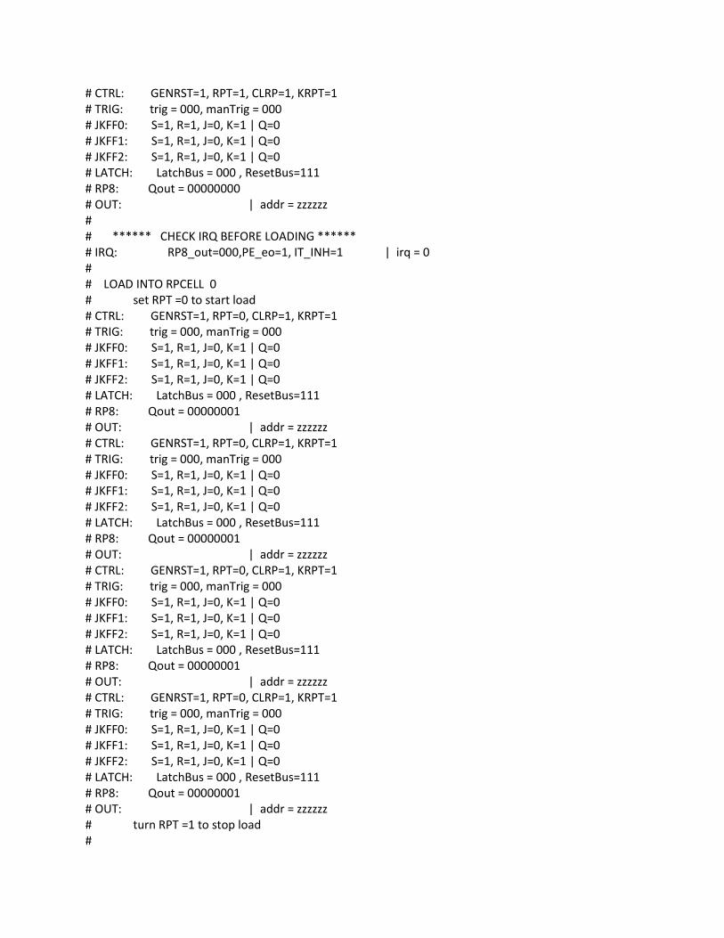
While there is an interrupt left to process, we repeat the following steps: 1) Check on the contents of the RPCells to see which interrupts have “fired”. This is indicated by the Q values shown. 2) Load the values of the single RPCells into RP8, the 8-bit state tracker. This result is labeled RP8’s Qout. 3) Enable RP8 output to write on the AddrBus. Make sure the correct address is written (depending on the particular input being processed). 4) Activate the KRPT signal to reset whichever interrupt has been processed. 5) Clear the contents of RP8 state register Generally, after using a particular control signal for a step, we disable it (eg KRPT gets disabled before we enter step 5). Scanning through the test print out in APPENDIX A, you can watch the Address Bus get periodically set (first to 2004, then to 2014, and finally to 2020). This corresponds to the desired addresses for TIME3, TIME4, and KBSTR. Since we fired all these simultaneously at the beginning, we observe that the module works correctly! We can successfully manage multiple interrupts at once. Also, keep an eye on the IRQ signal as the test progresses. Observe that it is disabled (irq=1) whenever the system has loaded RP8 and when the system is waiting for a reset or trigger action to happen. However, when a interrupt needs to be processed, the value of irq=0 (active), like when a new value needs to be loaded into the RP8.
CTR (PRIORITY COUNTER)
The CTR module’s purpose is to increment and decrement counters (which are simply memory locations) according to signals from elsewhere in the computer. The original Apollo Guidance computer contained 20 counters; we adhere to John Pultorak’s implementation and only include 5. Four of these counters interface with the control module and function as timers of some fashion. The remaining counter keeps track of overflows occurring for a particular subset of instructions. Certain counter overflows will trigger interrupts to the INT module.
CTRL: THE CONTROL LOGIC
CMI (CONTROL MODULE EXTERNAL INTERFACE)
The CMI is essentially the control wrapper that interfaces with all of the following control submodules. This was essentially just a single Verilog module that wires all the following bits together
MON (AGC MONITOR)
MON was obsorbed into the CTL. MON was a series of hardware switches and dials that we hard-wired to defaults in order to simplify the system. One example was the clock speed dial which we set to a fixed value for simplicty.

CLK (CLOCK)
GENERAL FUNCTIONALITY
The CLK module generates the two clock signals, CLK1 and CLK2. These are two normally low, out of phase, non overlapping clock signals used throughout the AGC. The module has inputs for the Reset signal, and the signals that determine if the clock runs automatically or is stepped by hand. However, since the AGC is being simulated, there is no need for the manual stepping, so that feature is not implemented.
SPECIFIC IMPLEMENTATION
The CLK has a 2 MHz internal clock that controls the flip flops that generate CLK1 and CLK2, resulting in 1 MHz outputs. These values are instead of the 2.048 MHz and 1.024 MHz values described in the schematic for ease of simulation.
TESTING
This module is the easiest to test of them all, since two of the inputs are not implemented and the other is a reset signal. Thus the test starts by asserting the reset signal, releasing it, and then monitoring CLK1 and CLK2. CLK2 is supposed to start first, and does as soon as the reset signal is turned off. CLK1 goes high a half cycle later, and the pattern repeats.
SCL (SCALER)
GENERAL FUNCTIONALITY
The scaler (SCL) module produces a series of oscillating signals based on the AGC system clock.
The output signals are labeled F1, F2, … F16. The signal FX represents a clock with frequency equal to CLK1/(10*2^X). So if the full cycle delay of CLK1 is 1000 time units, FX will take 2^X*10000 time units.

This module also contains three “one shot registers”. Each of these registers basically reads in one of the FX inputs (F10, F13, or F17 to be exact) and jumps to an activated state for one CLK1 cycle whenever its input signal goes through one period. This “one shot” thus acts like an alarm or timer that can be used by software (or hardware).
SPECIFIC IMPLEMENTATION:
The fundamental unit that allows the scaling of CLK1 is the synchronous counter chip 74LS161A. This is a 4 bit binary counter that will cycle from 0 to 15 decimal output when enabled. All changes in the count value occur on a positive edge of the clock (in this case CLK1). Chaining several of these together in a cascade allows for even higher counting ability by carefully setting the enable of one counter chip to only activate when the previous chip has reached its maximum value and starting over. The AGC requires 5 cascading counters.
We construct the FX signal of the SCL module by looking at the X bit of the counter output.
The one shot registers are each implemented using a series of JK flip flops.
TESTING
We verified this module using 2 separate tests.
First, we made sure the counter module worked and had the correct delay in relation to CLK1. Knowing the formula for when the Xth bit on the counter should first go from 0 to 1, we simply checked in on the counter at time 2^X*10*DELAY, where DELAY is the delay of CLK1 (in our case 1000 units). At these times the counter value should have X “1”s in its lowest order bits.
The print out below matches our expectations exactly.

# Initializing ... # START! # test counting ability # we'll check in on FBus every 2^i*10*DELAY time units # its should look like 000... followed by i 1s # 20000 | OUT = 00000000000000001 # 40000 | OUT = 00000000000000011 # 80000 | OUT = 00000000000000111 # 160000 | OUT = 00000000000001111 # 320000 | OUT = 00000000000011111 # 640000 | OUT = 00000000000111111 # 1280000 | OUT = 00000000001111111 # 2560000 | OUT = 00000000011111111 # 5120000 | OUT = 00000000111111111 # 10240000 | OUT = 00000001111111111 # 20480000 | OUT = 00000011111111111 # 40960000 | OUT = 00000111111111111 # 81920000 | OUT = 00001111111111111 # 163840000 | OUT = 00011111111111111 # 327680000 | OUT = 00111111111111111 # 655360000 | OUT = 01111111111111111 # 1310720000 | OUT = 11111111111111111
Second, we tested the ability of the “one shot” registers to fire appropriately. We examined both F17 and F10 separately. Recall that the “one shot” value will jump from 0 to 1 briefly when its corresponding pulse signal has a positive edge. We thus monitor the value of the one shot as the appropriate signal nears a positive edge (reusing some code from the above test). In both cases, we find that the one shot value jumps approximately one CLK1 cycle after F10 and F17 have a positive edge and then promptly resets the next CLK1 cycle, as expected.
# Initializing ... # START! # test one shot ability on F17 # we'll run simulation until F17 (10th bit on FBus) should go off # this should cause OneShotBus to flash to 100 for a brief time # 20000 | FBus = 00000000000000001 # 40000 | FBus = 00000000000000011 # 80000 | FBus = 00000000000000111 # 160000 | FBus = 00000000000001111 # 320000 | FBus = 00000000000011111 # 640000 | FBus = 00000000000111111 # 1280000 | FBus = 00000000001111111 # 2560000 | FBus = 00000000011111111 # 5120000 | FBus = 00000000111111111 # 10240000 | FBus = 00000001111111111 # 20480000 | FBus = 00000011111111111

# 40960000 | FBus = 00000111111111111 # 81920000 | FBus = 00001111111111111 # 163840000 | FBus = 00011111111111111 # 327680000 | FBus = 00111111111111111 # 655360000 | FBus = 01111111111111111 # 655360000 | FBus = 01111111111111111 | OneShot = 000 # 655360600 | FBus = 10000000000000000 | OneShot = 000 # 655361600 | FBus = 10000000000000000 | OneShot = 100 # 655362600 | FBus = 10000000000000000 | OneShot = 000 # Initializing ... # START! # test one shot ability on F10 # we'll run simulation until F10 (10th bit on FBus) should go off # this should cause OneShotBus to flash to 001 for a brief time # 20000 | FBus = 00000000000000001 # 40000 | FBus = 00000000000000011 # 80000 | FBus = 00000000000000111 # 160000 | FBus = 00000000000001111 # 320000 | FBus = 00000000000011111 # 640000 | FBus = 00000000000111111 # 1280000 | FBus = 00000000001111111 # 2560000 | FBus = 00000000011111111 # 5120000 | FBus = 00000000111111111 # 5120000 | FBus = 00000000111111111 | OneShot = 000 # 5120600 | FBus = 00000001000000000 | OneShot = 000 # 5121600 | FBus = 00000001000000000 | OneShot = 001 # 5122600 | FBus = 00000001000000000 | OneShot = 000 # 5130600 | FBus = 00000001000000001 | OneShot = 000 # 5140600 | FBus = 00000001000000010 | OneShot = 000
TPG (TIME PULSE GENERATOR)
In order to explain how the TPG works, let me first include a diagram from John Poltorak. The TPG is a big counter with a bunch of control logic to tell it when to count up and when to stay put.
We can see from the diagram that the TPG can sit in Standby, sit in a power-on clear, sit in SRLSE after the 12th count, or sit in a waiting state. The 10 control inputs tell the TPG when to wait where and for how long. The exact manner of this control is found on pages 40 and 41 of the CTL manual by John Poltorak.

In testing the TPG, the first main problem I ran into was a high vs low bit confusion in the counter contained within the module. I found the problem to be that I had assigned the bits backwards into the 74LS154 counter.
The final challenge was determining how the control inputs worked. Forcing the counter to move from the TP12 state shown in the diagram to the SRLSE state and into the WAIT state required changes in the control pins. After entering state TP12, the control NSTEP had to be toggled to 0 and back to 1 to force the counter into SRLSE. To move out of the SRLSE state, NSTEP had to once again be toggled while also changing NRUN to 1.
After discovering the necessity of changing inputs, the TPG was tested and ready to go.
SEQ (SEQUENCE GENERATOR)
GENERAL FUNCTIONALITY
The SEQ module is a control module. The output of this module helps determine what instruction gets executed next in the AGC CPU. Essentially, this module holds the registers that track the state of branching and other important execution processes such as the stage and the next instruction. It has registers for each of these state elements. We call these registers BR (branch), STA (stage), and SQ (Instruction Sequence). Its inputs are control signals that change the register values, which causes the CPU to change state.
SPECIFIC IMPLEMENTATION
The instruction register unit allows both loading a particular value for the next instruction or counting to reach the next instruction. The stage register unit uses a series of registers labeled A as buffers and maps their outputs to 2 registers B1 and B2 the form the actual output. The branch register unit consists of 2 registers, BR1, BR2. These hold the system’s current branching state.
TESTING
Testing this module conclusively proved difficult due to poor documentation. However, but toggling basic control signals we were able to identify some basic functionality and get the registers to do approximately their intended function. We’ll discuss the testing of each register group (Instruction, Stage, and branch) separately. Because the testing procedure is so long, we have included the individual test outputs in APPENDIX B.
CPM-A (CONTROL PULSE MATRIX A)
GENERAL FUNCTIONALITY

The CPMA is the core of the control logic. As the largest part of the CPM module which sets all 101 control flags, the CPMA is responsible for setting the first 56 control flags. Effectively, it does the work of translating the current instruction and state of the computer into the control signals that dictate the PROC module. The core of the CPMA is a large lookup table. Using this table, fourteen bits of input signal are translated into 56 bits of output signal. In hardware, this table is made using 7 EPROMs, each outputting eight bits. In simulation the table is contained in a precomputed data file made by modifying and running code that was provided to generate the tables for each of the EPROMs. Some logic is done to certain control signals after the EPROMs, but most feed directly into the control bus. The inputs to the module that form the 14 bit lookup address consist of: Bits 14-13: Two bits indicating if processing needs to be interrupted Bits 12-9: Four bits holding the currently executing instruction Bits 8-7: Two bits showing which subsequence of the current instruction is being run Bits 6-3: Four bit value that dictates what step of the subsequence is being run Bits 2-1: Two bit conditional branch register if more than one set of control pulses exists for the step The 56 bits of output contain 6 bits that are only used by CPMB and CPMC.
SPECIFIC IMPLEMENTATION
The seven EPROMs were replaced with one “56 bit EPROM” that loads from the precomputed data file and loads it into a table. It outputs the value indexed by the 14 bit value input to it.
TESTING
Testing this module was done mostly by testing the EPROM structure itself. Since the EPROM has one input and one output, it was very straightforward to test. A value was put on its input pins and the 56 bit output was printed to make sure it agreed with the appropriate step of the right instruction subsequence. A few values close together were tested as well to make sure there was no offset due to zero versus one indexing.
CPM-B (CONTROL PULSE MATRIX B)
The CMP-B module signals reads and writes to special registers, including the four central registers of the PROC module, as well as I/O registers. A portion of memory addresses are reserved for designating these registers, and this module ensures that the proper register is written to or read from.
CPM-C (CONTROL PULSE MATRIX C)
The CMP-C module interfaces with the priority counter and cycles through instructions
MEMORY
MMI (MEMORY MODULE EXTERNAL INTERFACE)

EMM/FMM (ERASABLE/FIXED MEMORY)
In an effort to simplify the computer, we faked memory using behavioral Verilog.
MBF (MEMORY BUFFER REGISTER)
The MBF module controls transfers between buses, registers, and memory. It will see to it that bits are shifted as necessary before being sent to the appropriate location. In particular, the MBF deals with parity and sign bits, which are stored in different bits depending on the word’s location.
PAR (PARITY GENERATE AND TEST)
The purpose of the PAR module is to both generate parity bits to tag memory contents, as well as to check parity bits to identify errors. Each 15 bit word in memory is accompanied by a 16th bit, selected to give the word an odd parity. Every memory cycle, parity bits are checked, and an alarm is set off if the word is found to be corrupt.
ADR (MEMORY ADDRESS)
GENERAL FUNCTIONALITY
The ADR module determines the next memory address the CPU needs to access. There are generally three different modes for determining the next address: LOAD FROM MEMORY: When the memory enable signal (AddrWrFrMem) is active (=1) and the load trigger (ExamTrig) is active (=1) then the ADR module loads whatever value is stored on the MemSwitch bus into the address bus (ABus). COUNT: When the memory signal is active but the load signal is inactive, the value of the Address bus is incremented by one every clock tick. This is probably the most common mode of the ADR, as many consecutive instructions are stored at consecutive locations in memory. WRITE BUS ENTRY: The latest value of the write bus (WBus) is always loaded into both the Bank register and the S register. S register is a 12 bit value that holds the lowest 12 bits of an address. Bank register is a 4 bit value that selects what memory bank (fixed or switchable) to address. According to John Pultorak

This selection process resolves through a series of basic logic gates (NOT, AND, OR) and ends of with final value held in the BankSelect bus. When the AddrWrFrMem signal is disabled (=0) the address bus obtains its next value from both the BankSelect bus and the S Register output. The top four bits (14-11) are from the BankSelect, while the bottom 10 come straight from the S register. Separate controls (WS and WBK) govern when the S and BankSelect registers can write onto the address bus. Additionally, the ADR module can write the top four bits of the write bus to the read bus when enabled. This action synchronizes with a falling edge on CLK1.
TESTING
We tested each mode of the ADR module in turn. While exhaustive testing was impossible, we verified basic functionality of each mode. First, we verified that the LOAD mode executed as expected. We see that the Address Bus does load the value of the MemSwitch bus after a clock cycle when triggered properly. # ------- MEM SWITCH ENTRY ---- # trigger mem load into addr # ExamTrig=1 | MemSwitch = 01010101000000 # | ABus = 01010101000000 Next, we verified that the address bus would increment when the load trigger turned off. We see the Address Bus properly count from the loaded value over 8 clock cycles. # ------- COUNT ---- # disable trigger. should just count. # ExamTrig=0 | MemSwitch = 01010101000000 # | ABus = 01010101000010 # | ABus = 01010101000011 # | ABus = 01010101000100 # | ABus = 01010101000101 # | ABus = 01010101000110 # | ABus = 01010101000111 # | ABus = 01010101001000

# | ABus = 01010101001001 Finally, we verified that the process of writing to the address bus from the S and BNK registers succeeds. While not an exhaustive test, we do see that the separate write controls for S and BNK do have their desired effect in altering the address bus. # ------- WRITE BUS ENTRY ---- # Switch source from Mem to Bank/S registers # WBus=11110000111100 # | ABus = 00000000000000 # enable writing to S # WBus=11110000111100 # | ABus = 00110000111100 # enable writing to BNK # WBus=11110000111100 # | ABus = 11110000111100 The ADR module will push the highest four bits of the BNK value into bits 14-11 of the 16 bit read bus. We verify that we can properly write on the ReadBus when we enable the writing process, when must happen on a falling edge of CLK1. We see the top four bits of the WBus do indeed make it to the R Bus, as expected. # ------- READ BUS ACTIVE ---- # check RBus before RBK changes # WBus=11110000111100 # | RBus = zzzzzzzzzzzzzzzz # check RBus after RBK =0, CLK1 = 1 # WBus=11110000111100 # | RBus = zzzzzzzzzzzzzzzz # check RBus after RBK=0, CLK1=0 # this should change RBus. can only work on falling CLK1 edge # WBus=11110000111100 # | RBus = 0011110000000000
CHIPS
74LS151
Enabled 8 to 1 multiplexer; when the enable bit is low, this multiplexer outputs the value of the particular input bit indicated by three selector bits. This was not tested exhaustively; however, 16 input combinations were tested for each of the enabled and un-enabled states. These tests confirmed that the enable is functional, that the correct bit is always selected, and that the output will be high or low as specified by the selected input.
74LS138

Enabled 3 to 8 demultiplexer; uses 3 select bits and 3 enable bits as inputs, and outputs an 8 bit signal. The enabled state occurs when the first enable bit is high and the remaining two are low. There are 8 possible combinations of select bits; each of these was tested for the enabled state. When the demultiplexer is not enabled (for 7 out of 8 of the possible enable bit combinations), all 8 of the output bits should be high regardless of the select bits; this was tested exhaustively.
74LS148
8-line to 3-line priority encoder; is used to identify the most significant bit of 8 input bits that is high. While the priority encoder was not exhaustively tested, it was tested in the enabled state (enable bit = 0) for one case per expected output combination. These same cases were then tested for the un-enabled state to ensure that the enable was working properly.
74LS273
8 flip flops, resets when MR is LOW.
74LS83A
Full 4 bit full adder
74LS181
Gate can do both math and logic, but is wired to only do logic since M is high. In addition to input/outputs listed below, also outputs Cn+4, A=B, G, and P.
74LS244
8 bit delay module with active-low enable
74LS161A
4 bit synchronous counter with parallel load feature
74LS154
4 to 16 DeMUX
74S280
9 Bit Parity Generator/Checker - This chip has two outputs: an odd indicator and an even indicator. The odd indicator will be high when an odd number of the nine inputs are high; the even indicator will be high when an even number of nine inputs are high. This was fairly easy to test exhaustively, by simply

running through all of the possible 9-bit input combinations in numerical order and confirming that the parities identified by the outputs are correct.
TOOLS AND RESOURCES
Because this guide is meant to help those wishing for a more complete understanding of the AGC we have included descriptions of our tools and resources. We have already mentioned the klabs.org website and the guides written by John Pultorak both of which were invaluable. The verilog was written primarially in Notepad++ and simulated in ModelSim.
APPENDIX A
# # ------- TRIAL = 0 / 3 # # # ****** CHECK IRQ IN WAIT MODE ****** # IRQ: RP8_out=000,PE_eo=0, IT_INH=1 | irq = 1 # # FIRE 000 # CTRL: GENRST=1, RPT=1, CLRP=1, KRPT=1 # TRIG: trig = 000, manTrig = 000 # JKFF0: S=1, R=1, J=0, K=1 | Q=0 # JKFF1: S=1, R=1, J=0, K=1 | Q=0 # JKFF2: S=1, R=1, J=0, K=1 | Q=0 # LATCH: LatchBus = 000 , ResetBus=111 # RP8: Qout = 00000000 # OUT: | addr = zzzzzz # CTRL: GENRST=1, RPT=1, CLRP=1, KRPT=1 # TRIG: trig = 000, manTrig = 000 # JKFF0: S=1, R=1, J=0, K=1 | Q=0 # JKFF1: S=1, R=1, J=0, K=1 | Q=0 # JKFF2: S=1, R=1, J=0, K=1 | Q=0 # LATCH: LatchBus = 000 , ResetBus=111 # RP8: Qout = 00000000 # OUT: | addr = zzzzzz # CTRL: GENRST=1, RPT=1, CLRP=1, KRPT=1 # TRIG: trig = 000, manTrig = 000 # JKFF0: S=1, R=1, J=0, K=1 | Q=0 # JKFF1: S=1, R=1, J=0, K=1 | Q=0 # JKFF2: S=1, R=1, J=0, K=1 | Q=0 # LATCH: LatchBus = 000 , ResetBus=111 # RP8: Qout = 00000000 # OUT: | addr = zzzzzz
# CTRL: GENRST=1, RPT=1, CLRP=1, KRPT=1 # TRIG: trig = 000, manTrig = 000 # JKFF0: S=1, R=1, J=0, K=1 | Q=0 # JKFF1: S=1, R=1, J=0, K=1 | Q=0 # JKFF2: S=1, R=1, J=0, K=1 | Q=0 # LATCH: LatchBus = 000 , ResetBus=111 # RP8: Qout = 00000000 # OUT: | addr = zzzzzz # # ****** CHECK IRQ BEFORE LOADING ****** # IRQ: RP8_out=000,PE_eo=1, IT_INH=1 | irq = 0 # # LOAD INTO RPCELL 0 # set RPT =0 to start load # CTRL: GENRST=1, RPT=0, CLRP=1, KRPT=1 # TRIG: trig = 000, manTrig = 000 # JKFF0: S=1, R=1, J=0, K=1 | Q=0 # JKFF1: S=1, R=1, J=0, K=1 | Q=0 # JKFF2: S=1, R=1, J=0, K=1 | Q=0 # LATCH: LatchBus = 000 , ResetBus=111 # RP8: Qout = 00000001 # OUT: | addr = zzzzzz # CTRL: GENRST=1, RPT=0, CLRP=1, KRPT=1 # TRIG: trig = 000, manTrig = 000 # JKFF0: S=1, R=1, J=0, K=1 | Q=0 # JKFF1: S=1, R=1, J=0, K=1 | Q=0 # JKFF2: S=1, R=1, J=0, K=1 | Q=0 # LATCH: LatchBus = 000 , ResetBus=111 # RP8: Qout = 00000001 # OUT: | addr = zzzzzz # CTRL: GENRST=1, RPT=0, CLRP=1, KRPT=1 # TRIG: trig = 000, manTrig = 000 # JKFF0: S=1, R=1, J=0, K=1 | Q=0 # JKFF1: S=1, R=1, J=0, K=1 | Q=0 # JKFF2: S=1, R=1, J=0, K=1 | Q=0 # LATCH: LatchBus = 000 , ResetBus=111 # RP8: Qout = 00000001 # OUT: | addr = zzzzzz # CTRL: GENRST=1, RPT=0, CLRP=1, KRPT=1 # TRIG: trig = 000, manTrig = 000 # JKFF0: S=1, R=1, J=0, K=1 | Q=0 # JKFF1: S=1, R=1, J=0, K=1 | Q=0 # JKFF2: S=1, R=1, J=0, K=1 | Q=0 # LATCH: LatchBus = 000 , ResetBus=111 # RP8: Qout = 00000001 # OUT: | addr = zzzzzz # turn RPT =1 to stop load #

# ****** CHECK IRQ NOW THAT ITS LOADED ****** # IRQ: RP8_out=001,PE_eo=1, IT_INH=1 | irq = 1 # # ENABLE LOAD INTO ADDR OUT # CTRL: GENRST=1, RPT=1, CLRP=1, KRPT=1 # TRIG: trig = 111, manTrig = 000 # JKFF0: S=1, R=1, J=0, K=1 | Q=0 # JKFF1: S=1, R=1, J=0, K=1 | Q=0 # JKFF2: S=1, R=1, J=0, K=1 | Q=0 # LATCH: LatchBus = 000 , ResetBus=111 # RP8: Qout = 00000001 # OUT: | addr = 002004 # CTRL: GENRST=1, RPT=1, CLRP=1, KRPT=1 # TRIG: trig = 111, manTrig = 000 # JKFF0: S=1, R=1, J=0, K=1 | Q=0 # JKFF1: S=1, R=1, J=0, K=1 | Q=0 # JKFF2: S=1, R=1, J=0, K=1 | Q=0 # LATCH: LatchBus = 000 , ResetBus=111 # RP8: Qout = 00000001 # OUT: | addr = 002004 # CTRL: GENRST=1, RPT=1, CLRP=1, KRPT=1 # TRIG: trig = 111, manTrig = 000 # JKFF0: S=1, R=1, J=0, K=1 | Q=0 # JKFF1: S=1, R=1, J=0, K=1 | Q=0 # JKFF2: S=1, R=1, J=0, K=1 | Q=0 # LATCH: LatchBus = 000 , ResetBus=111 # RP8: Qout = 00000001 # OUT: | addr = 002004 # CTRL: GENRST=1, RPT=1, CLRP=1, KRPT=1 # TRIG: trig = 111, manTrig = 000 # JKFF0: S=1, R=1, J=0, K=1 | Q=0 # JKFF1: S=1, R=1, J=0, K=1 | Q=0 # JKFF2: S=1, R=1, J=0, K=1 | Q=0 # LATCH: LatchBus = 000 , ResetBus=111 # RP8: Qout = 00000001 # OUT: | addr = 002004 # # RESET # CTRL: GENRST=1, RPT=1, CLRP=1, KRPT=0 # TRIG: trig = 111, manTrig = 000 # JKFF0: S=0, R=1, J=0, K=1 | Q=1 # JKFF1: S=1, R=1, J=0, K=1 | Q=0 # JKFF2: S=1, R=1, J=0, K=1 | Q=0 # LATCH: LatchBus = 001 , ResetBus=110 # RP8: Qout = 00000001 # OUT: | addr = zzzzzz # CTRL: GENRST=1, RPT=1, CLRP=1, KRPT=0 # TRIG: trig = 111, manTrig = 000

# JKFF0: S=1, R=1, J=0, K=1 | Q=1 # JKFF1: S=1, R=1, J=0, K=1 | Q=0 # JKFF2: S=1, R=1, J=0, K=1 | Q=0 # LATCH: LatchBus = 001 , ResetBus=111 # RP8: Qout = 00000001 # OUT: | addr = zzzzzz # CTRL: GENRST=1, RPT=1, CLRP=1, KRPT=0 # TRIG: trig = 111, manTrig = 000 # JKFF0: S=0, R=1, J=0, K=1 | Q=1 # JKFF1: S=1, R=1, J=0, K=1 | Q=0 # JKFF2: S=1, R=1, J=0, K=1 | Q=0 # LATCH: LatchBus = 001 , ResetBus=110 # RP8: Qout = 00000001 # OUT: | addr = zzzzzz # CTRL: GENRST=1, RPT=1, CLRP=1, KRPT=0 # TRIG: trig = 111, manTrig = 000 # JKFF0: S=1, R=1, J=0, K=1 | Q=1 # JKFF1: S=1, R=1, J=0, K=1 | Q=0 # JKFF2: S=1, R=1, J=0, K=1 | Q=0 # LATCH: LatchBus = 001 , ResetBus=111 # RP8: Qout = 00000001 # OUT: | addr = zzzzzz # # CLEAR RP8 # CTRL: GENRST=1, RPT=1, CLRP=0, KRPT=1 # TRIG: trig = 111, manTrig = 000 # JKFF0: S=1, R=1, J=0, K=1 | Q=1 # JKFF1: S=1, R=1, J=0, K=1 | Q=0 # JKFF2: S=1, R=1, J=0, K=1 | Q=0 # LATCH: LatchBus = 001 , ResetBus=111 # RP8: Qout = 00000000 # OUT: | addr = zzzzzz # CTRL: GENRST=1, RPT=1, CLRP=0, KRPT=1 # TRIG: trig = 111, manTrig = 000 # JKFF0: S=1, R=1, J=0, K=1 | Q=1 # JKFF1: S=1, R=1, J=0, K=1 | Q=0 # JKFF2: S=1, R=1, J=0, K=1 | Q=0 # LATCH: LatchBus = 001 , ResetBus=111 # RP8: Qout = 00000000 # OUT: | addr = zzzzzz # CTRL: GENRST=1, RPT=1, CLRP=0, KRPT=1 # TRIG: trig = 111, manTrig = 000 # JKFF0: S=1, R=1, J=0, K=1 | Q=1 # JKFF1: S=1, R=1, J=0, K=1 | Q=0 # JKFF2: S=1, R=1, J=0, K=1 | Q=0 # LATCH: LatchBus = 001 , ResetBus=111 # RP8: Qout = 00000000 # OUT: | addr = zzzzzz

# CTRL: GENRST=1, RPT=1, CLRP=0, KRPT=1 # TRIG: trig = 111, manTrig = 000 # JKFF0: S=1, R=1, J=0, K=1 | Q=1 # JKFF1: S=1, R=1, J=0, K=1 | Q=0 # JKFF2: S=1, R=1, J=0, K=1 | Q=0 # LATCH: LatchBus = 001 , ResetBus=111 # RP8: Qout = 00000000 # OUT: | addr = zzzzzz # # WAIT MODE # CTRL: GENRST=1, RPT=1, CLRP=1, KRPT=1 # TRIG: trig = 111, manTrig = 000 # JKFF0: S=1, R=1, J=0, K=1 | Q=1 # JKFF1: S=1, R=1, J=0, K=1 | Q=0 # JKFF2: S=1, R=1, J=0, K=1 | Q=0 # LATCH: LatchBus = 001 , ResetBus=111 # RP8: Qout = 00000000 # OUT: | addr = zzzzzz # CTRL: GENRST=1, RPT=1, CLRP=1, KRPT=1 # TRIG: trig = 111, manTrig = 000 # JKFF0: S=1, R=1, J=0, K=1 | Q=1 # JKFF1: S=1, R=1, J=0, K=1 | Q=0 # JKFF2: S=1, R=1, J=0, K=1 | Q=0 # LATCH: LatchBus = 001 , ResetBus=111 # RP8: Qout = 00000000 # OUT: | addr = zzzzzz # CTRL: GENRST=1, RPT=1, CLRP=1, KRPT=1 # TRIG: trig = 111, manTrig = 000 # JKFF0: S=1, R=1, J=0, K=1 | Q=1 # JKFF1: S=1, R=1, J=0, K=1 | Q=0 # JKFF2: S=1, R=1, J=0, K=1 | Q=0 # LATCH: LatchBus = 001 , ResetBus=111 # RP8: Qout = 00000000 # OUT: | addr = zzzzzz # CTRL: GENRST=1, RPT=1, CLRP=1, KRPT=1 # TRIG: trig = 111, manTrig = 000 # JKFF0: S=1, R=1, J=0, K=1 | Q=1 # JKFF1: S=1, R=1, J=0, K=1 | Q=0 # JKFF2: S=1, R=1, J=0, K=1 | Q=0 # LATCH: LatchBus = 001 , ResetBus=111 # RP8: Qout = 00000000 # OUT: | addr = zzzzzz # # # # ------- TRIAL = 1 / 3 # #

# ****** CHECK IRQ IN WAIT MODE ****** # IRQ: RP8_out=000,PE_eo=1, IT_INH=1 | irq = 0 # # FIRE 000 # CTRL: GENRST=1, RPT=1, CLRP=1, KRPT=1 # TRIG: trig = 111, manTrig = 000 # JKFF0: S=1, R=1, J=0, K=1 | Q=1 # JKFF1: S=1, R=1, J=0, K=1 | Q=0 # JKFF2: S=1, R=1, J=0, K=1 | Q=0 # LATCH: LatchBus = 001 , ResetBus=111 # RP8: Qout = 00000000 # OUT: | addr = zzzzzz # CTRL: GENRST=1, RPT=1, CLRP=1, KRPT=1 # TRIG: trig = 111, manTrig = 000 # JKFF0: S=1, R=1, J=0, K=1 | Q=1 # JKFF1: S=1, R=1, J=0, K=1 | Q=0 # JKFF2: S=1, R=1, J=0, K=1 | Q=0 # LATCH: LatchBus = 001 , ResetBus=111 # RP8: Qout = 00000000 # OUT: | addr = zzzzzz # CTRL: GENRST=1, RPT=1, CLRP=1, KRPT=1 # TRIG: trig = 111, manTrig = 000 # JKFF0: S=1, R=1, J=0, K=1 | Q=1 # JKFF1: S=1, R=1, J=0, K=1 | Q=0 # JKFF2: S=1, R=1, J=0, K=1 | Q=0 # LATCH: LatchBus = 001 , ResetBus=111 # RP8: Qout = 00000000 # OUT: | addr = zzzzzz # CTRL: GENRST=1, RPT=1, CLRP=1, KRPT=1 # TRIG: trig = 111, manTrig = 000 # JKFF0: S=1, R=1, J=0, K=1 | Q=1 # JKFF1: S=1, R=1, J=0, K=1 | Q=0 # JKFF2: S=1, R=1, J=0, K=1 | Q=0 # LATCH: LatchBus = 001 , ResetBus=111 # RP8: Qout = 00000000 # OUT: | addr = zzzzzz # # ****** CHECK IRQ BEFORE LOADING ****** # IRQ: RP8_out=000,PE_eo=1, IT_INH=1 | irq = 0 # # LOAD INTO RPCELL 0 # set RPT =0 to start load # CTRL: GENRST=1, RPT=0, CLRP=1, KRPT=1 # TRIG: trig = 111, manTrig = 000 # JKFF0: S=1, R=1, J=0, K=1 | Q=1 # JKFF1: S=1, R=1, J=0, K=1 | Q=0 # JKFF2: S=1, R=1, J=0, K=1 | Q=0 # LATCH: LatchBus = 001 , ResetBus=111

# RP8: Qout = 00000011 # OUT: | addr = zzzzzz # CTRL: GENRST=1, RPT=0, CLRP=1, KRPT=1 # TRIG: trig = 111, manTrig = 000 # JKFF0: S=1, R=1, J=0, K=1 | Q=1 # JKFF1: S=1, R=1, J=0, K=1 | Q=0 # JKFF2: S=1, R=1, J=0, K=1 | Q=0 # LATCH: LatchBus = 001 , ResetBus=111 # RP8: Qout = 00000011 # OUT: | addr = zzzzzz # CTRL: GENRST=1, RPT=0, CLRP=1, KRPT=1 # TRIG: trig = 111, manTrig = 000 # JKFF0: S=1, R=1, J=0, K=1 | Q=1 # JKFF1: S=1, R=1, J=0, K=1 | Q=0 # JKFF2: S=1, R=1, J=0, K=1 | Q=0 # LATCH: LatchBus = 001 , ResetBus=111 # RP8: Qout = 00000011 # OUT: | addr = zzzzzz # CTRL: GENRST=1, RPT=0, CLRP=1, KRPT=1 # TRIG: trig = 111, manTrig = 000 # JKFF0: S=1, R=1, J=0, K=1 | Q=1 # JKFF1: S=1, R=1, J=0, K=1 | Q=0 # JKFF2: S=1, R=1, J=0, K=1 | Q=0 # LATCH: LatchBus = 001 , ResetBus=111 # RP8: Qout = 00000011 # OUT: | addr = zzzzzz # turn RPT =1 to stop load # # ****** CHECK IRQ NOW THAT ITS LOADED ****** # IRQ: RP8_out=011,PE_eo=1, IT_INH=1 | irq = 1 # # ENABLE LOAD INTO ADDR OUT # CTRL: GENRST=1, RPT=1, CLRP=1, KRPT=1 # TRIG: trig = 111, manTrig = 000 # JKFF0: S=1, R=1, J=0, K=1 | Q=1 # JKFF1: S=1, R=1, J=0, K=1 | Q=0 # JKFF2: S=1, R=1, J=0, K=1 | Q=0 # LATCH: LatchBus = 001 , ResetBus=111 # RP8: Qout = 00000011 # OUT: | addr = 002014 # CTRL: GENRST=1, RPT=1, CLRP=1, KRPT=1 # TRIG: trig = 111, manTrig = 000 # JKFF0: S=1, R=1, J=0, K=1 | Q=1 # JKFF1: S=1, R=1, J=0, K=1 | Q=0 # JKFF2: S=1, R=1, J=0, K=1 | Q=0 # LATCH: LatchBus = 001 , ResetBus=111 # RP8: Qout = 00000011 # OUT: | addr = 002014

# CTRL: GENRST=1, RPT=1, CLRP=1, KRPT=1 # TRIG: trig = 111, manTrig = 000 # JKFF0: S=1, R=1, J=0, K=1 | Q=1 # JKFF1: S=1, R=1, J=0, K=1 | Q=0 # JKFF2: S=1, R=1, J=0, K=1 | Q=0 # LATCH: LatchBus = 001 , ResetBus=111 # RP8: Qout = 00000011 # OUT: | addr = 002014 # CTRL: GENRST=1, RPT=1, CLRP=1, KRPT=1 # TRIG: trig = 111, manTrig = 000 # JKFF0: S=1, R=1, J=0, K=1 | Q=1 # JKFF1: S=1, R=1, J=0, K=1 | Q=0 # JKFF2: S=1, R=1, J=0, K=1 | Q=0 # LATCH: LatchBus = 001 , ResetBus=111 # RP8: Qout = 00000011 # OUT: | addr = 002014 # # RESET # CTRL: GENRST=1, RPT=1, CLRP=1, KRPT=0 # TRIG: trig = 111, manTrig = 000 # JKFF0: S=1, R=1, J=0, K=1 | Q=1 # JKFF1: S=0, R=1, J=0, K=1 | Q=1 # JKFF2: S=1, R=1, J=0, K=1 | Q=0 # LATCH: LatchBus = 011 , ResetBus=101 # RP8: Qout = 00000011 # OUT: | addr = zzzzzz # CTRL: GENRST=1, RPT=1, CLRP=1, KRPT=0 # TRIG: trig = 111, manTrig = 000 # JKFF0: S=1, R=1, J=0, K=1 | Q=1 # JKFF1: S=1, R=1, J=0, K=1 | Q=1 # JKFF2: S=1, R=1, J=0, K=1 | Q=0 # LATCH: LatchBus = 011 , ResetBus=111 # RP8: Qout = 00000011 # OUT: | addr = zzzzzz # CTRL: GENRST=1, RPT=1, CLRP=1, KRPT=0 # TRIG: trig = 111, manTrig = 000 # JKFF0: S=1, R=1, J=0, K=1 | Q=1 # JKFF1: S=0, R=1, J=0, K=1 | Q=1 # JKFF2: S=1, R=1, J=0, K=1 | Q=0 # LATCH: LatchBus = 011 , ResetBus=101 # RP8: Qout = 00000011 # OUT: | addr = zzzzzz # CTRL: GENRST=1, RPT=1, CLRP=1, KRPT=0 # TRIG: trig = 111, manTrig = 000 # JKFF0: S=1, R=1, J=0, K=1 | Q=1 # JKFF1: S=1, R=1, J=0, K=1 | Q=1 # JKFF2: S=1, R=1, J=0, K=1 | Q=0 # LATCH: LatchBus = 011 , ResetBus=111

# RP8: Qout = 00000011 # OUT: | addr = zzzzzz # # CLEAR RP8 # CTRL: GENRST=1, RPT=1, CLRP=0, KRPT=1 # TRIG: trig = 111, manTrig = 000 # JKFF0: S=1, R=1, J=0, K=1 | Q=1 # JKFF1: S=1, R=1, J=0, K=1 | Q=1 # JKFF2: S=1, R=1, J=0, K=1 | Q=0 # LATCH: LatchBus = 011 , ResetBus=111 # RP8: Qout = 00000000 # OUT: | addr = zzzzzz # CTRL: GENRST=1, RPT=1, CLRP=0, KRPT=1 # TRIG: trig = 111, manTrig = 000 # JKFF0: S=1, R=1, J=0, K=1 | Q=1 # JKFF1: S=1, R=1, J=0, K=1 | Q=1 # JKFF2: S=1, R=1, J=0, K=1 | Q=0 # LATCH: LatchBus = 011 , ResetBus=111 # RP8: Qout = 00000000 # OUT: | addr = zzzzzz # CTRL: GENRST=1, RPT=1, CLRP=0, KRPT=1 # TRIG: trig = 111, manTrig = 000 # JKFF0: S=1, R=1, J=0, K=1 | Q=1 # JKFF1: S=1, R=1, J=0, K=1 | Q=1 # JKFF2: S=1, R=1, J=0, K=1 | Q=0 # LATCH: LatchBus = 011 , ResetBus=111 # RP8: Qout = 00000000 # OUT: | addr = zzzzzz # CTRL: GENRST=1, RPT=1, CLRP=0, KRPT=1 # TRIG: trig = 111, manTrig = 000 # JKFF0: S=1, R=1, J=0, K=1 | Q=1 # JKFF1: S=1, R=1, J=0, K=1 | Q=1 # JKFF2: S=1, R=1, J=0, K=1 | Q=0 # LATCH: LatchBus = 011 , ResetBus=111 # RP8: Qout = 00000000 # OUT: | addr = zzzzzz # # WAIT MODE # CTRL: GENRST=1, RPT=1, CLRP=1, KRPT=1 # TRIG: trig = 111, manTrig = 000 # JKFF0: S=1, R=1, J=0, K=1 | Q=1 # JKFF1: S=1, R=1, J=0, K=1 | Q=1 # JKFF2: S=1, R=1, J=0, K=1 | Q=0 # LATCH: LatchBus = 011 , ResetBus=111 # RP8: Qout = 00000000 # OUT: | addr = zzzzzz # CTRL: GENRST=1, RPT=1, CLRP=1, KRPT=1 # TRIG: trig = 111, manTrig = 000

# JKFF0: S=1, R=1, J=0, K=1 | Q=1 # JKFF1: S=1, R=1, J=0, K=1 | Q=1 # JKFF2: S=1, R=1, J=0, K=1 | Q=0 # LATCH: LatchBus = 011 , ResetBus=111 # RP8: Qout = 00000000 # OUT: | addr = zzzzzz # CTRL: GENRST=1, RPT=1, CLRP=1, KRPT=1 # TRIG: trig = 111, manTrig = 000 # JKFF0: S=1, R=1, J=0, K=1 | Q=1 # JKFF1: S=1, R=1, J=0, K=1 | Q=1 # JKFF2: S=1, R=1, J=0, K=1 | Q=0 # LATCH: LatchBus = 011 , ResetBus=111 # RP8: Qout = 00000000 # OUT: | addr = zzzzzz # CTRL: GENRST=1, RPT=1, CLRP=1, KRPT=1 # TRIG: trig = 111, manTrig = 000 # JKFF0: S=1, R=1, J=0, K=1 | Q=1 # JKFF1: S=1, R=1, J=0, K=1 | Q=1 # JKFF2: S=1, R=1, J=0, K=1 | Q=0 # LATCH: LatchBus = 011 , ResetBus=111 # RP8: Qout = 00000000 # OUT: | addr = zzzzzz # # # # ------- TRIAL = 2 / 3 # # # ****** CHECK IRQ IN WAIT MODE ****** # IRQ: RP8_out=000,PE_eo=1, IT_INH=1 | irq = 0 # # FIRE 000 # CTRL: GENRST=1, RPT=1, CLRP=1, KRPT=1 # TRIG: trig = 111, manTrig = 000 # JKFF0: S=1, R=1, J=0, K=1 | Q=1 # JKFF1: S=1, R=1, J=0, K=1 | Q=1 # JKFF2: S=1, R=1, J=0, K=1 | Q=0 # LATCH: LatchBus = 011 , ResetBus=111 # RP8: Qout = 00000000 # OUT: | addr = zzzzzz # CTRL: GENRST=1, RPT=1, CLRP=1, KRPT=1 # TRIG: trig = 111, manTrig = 000 # JKFF0: S=1, R=1, J=0, K=1 | Q=1 # JKFF1: S=1, R=1, J=0, K=1 | Q=1 # JKFF2: S=1, R=1, J=0, K=1 | Q=0 # LATCH: LatchBus = 011 , ResetBus=111 # RP8: Qout = 00000000 # OUT: | addr = zzzzzz

# CTRL: GENRST=1, RPT=1, CLRP=1, KRPT=1 # TRIG: trig = 111, manTrig = 000 # JKFF0: S=1, R=1, J=0, K=1 | Q=1 # JKFF1: S=1, R=1, J=0, K=1 | Q=1 # JKFF2: S=1, R=1, J=0, K=1 | Q=0 # LATCH: LatchBus = 011 , ResetBus=111 # RP8: Qout = 00000000 # OUT: | addr = zzzzzz # CTRL: GENRST=1, RPT=1, CLRP=1, KRPT=1 # TRIG: trig = 111, manTrig = 000 # JKFF0: S=1, R=1, J=0, K=1 | Q=1 # JKFF1: S=1, R=1, J=0, K=1 | Q=1 # JKFF2: S=1, R=1, J=0, K=1 | Q=0 # LATCH: LatchBus = 011 , ResetBus=111 # RP8: Qout = 00000000 # OUT: | addr = zzzzzz # # ****** CHECK IRQ BEFORE LOADING ****** # IRQ: RP8_out=000,PE_eo=1, IT_INH=1 | irq = 0 # # LOAD INTO RPCELL 0 # set RPT =0 to start load # CTRL: GENRST=1, RPT=0, CLRP=1, KRPT=1 # TRIG: trig = 111, manTrig = 000 # JKFF0: S=1, R=1, J=0, K=1 | Q=1 # JKFF1: S=1, R=1, J=0, K=1 | Q=1 # JKFF2: S=1, R=1, J=0, K=1 | Q=0 # LATCH: LatchBus = 011 , ResetBus=111 # RP8: Qout = 00000100 # OUT: | addr = zzzzzz # CTRL: GENRST=1, RPT=0, CLRP=1, KRPT=1 # TRIG: trig = 111, manTrig = 000 # JKFF0: S=1, R=1, J=0, K=1 | Q=1 # JKFF1: S=1, R=1, J=0, K=1 | Q=1 # JKFF2: S=1, R=1, J=0, K=1 | Q=0 # LATCH: LatchBus = 011 , ResetBus=111 # RP8: Qout = 00000100 # OUT: | addr = zzzzzz # CTRL: GENRST=1, RPT=0, CLRP=1, KRPT=1 # TRIG: trig = 111, manTrig = 000 # JKFF0: S=1, R=1, J=0, K=1 | Q=1 # JKFF1: S=1, R=1, J=0, K=1 | Q=1 # JKFF2: S=1, R=1, J=0, K=1 | Q=0 # LATCH: LatchBus = 011 , ResetBus=111 # RP8: Qout = 00000100 # OUT: | addr = zzzzzz # CTRL: GENRST=1, RPT=0, CLRP=1, KRPT=1 # TRIG: trig = 111, manTrig = 000

# JKFF0: S=1, R=1, J=0, K=1 | Q=1 # JKFF1: S=1, R=1, J=0, K=1 | Q=1 # JKFF2: S=1, R=1, J=0, K=1 | Q=0 # LATCH: LatchBus = 011 , ResetBus=111 # RP8: Qout = 00000100 # OUT: | addr = zzzzzz # turn RPT =1 to stop load # # ****** CHECK IRQ NOW THAT ITS LOADED ****** # IRQ: RP8_out=100,PE_eo=1, IT_INH=1 | irq = 1 # # ENABLE LOAD INTO ADDR OUT # CTRL: GENRST=1, RPT=1, CLRP=1, KRPT=1 # TRIG: trig = 111, manTrig = 000 # JKFF0: S=1, R=1, J=0, K=1 | Q=1 # JKFF1: S=1, R=1, J=0, K=1 | Q=1 # JKFF2: S=1, R=1, J=0, K=1 | Q=0 # LATCH: LatchBus = 011 , ResetBus=111 # RP8: Qout = 00000100 # OUT: | addr = 002020 # CTRL: GENRST=1, RPT=1, CLRP=1, KRPT=1 # TRIG: trig = 111, manTrig = 000 # JKFF0: S=1, R=1, J=0, K=1 | Q=1 # JKFF1: S=1, R=1, J=0, K=1 | Q=1 # JKFF2: S=1, R=1, J=0, K=1 | Q=0 # LATCH: LatchBus = 011 , ResetBus=111 # RP8: Qout = 00000100 # OUT: | addr = 002020 # CTRL: GENRST=1, RPT=1, CLRP=1, KRPT=1 # TRIG: trig = 111, manTrig = 000 # JKFF0: S=1, R=1, J=0, K=1 | Q=1 # JKFF1: S=1, R=1, J=0, K=1 | Q=1 # JKFF2: S=1, R=1, J=0, K=1 | Q=0 # LATCH: LatchBus = 011 , ResetBus=111 # RP8: Qout = 00000100 # OUT: | addr = 002020 # CTRL: GENRST=1, RPT=1, CLRP=1, KRPT=1 # TRIG: trig = 111, manTrig = 000 # JKFF0: S=1, R=1, J=0, K=1 | Q=1 # JKFF1: S=1, R=1, J=0, K=1 | Q=1 # JKFF2: S=1, R=1, J=0, K=1 | Q=0 # LATCH: LatchBus = 011 , ResetBus=111 # RP8: Qout = 00000100 # OUT: | addr = 002020 # # RESET # CTRL: GENRST=1, RPT=1, CLRP=1, KRPT=0 # TRIG: trig = 111, manTrig = 000

# JKFF0: S=1, R=1, J=0, K=1 | Q=1 # JKFF1: S=1, R=1, J=0, K=1 | Q=1 # JKFF2: S=0, R=1, J=0, K=1 | Q=1 # LATCH: LatchBus = 111 , ResetBus=011 # RP8: Qout = 00000100 # OUT: | addr = zzzzzz # CTRL: GENRST=1, RPT=1, CLRP=1, KRPT=0 # TRIG: trig = 111, manTrig = 000 # JKFF0: S=1, R=1, J=0, K=1 | Q=1 # JKFF1: S=1, R=1, J=0, K=1 | Q=1 # JKFF2: S=1, R=1, J=0, K=1 | Q=1 # LATCH: LatchBus = 111 , ResetBus=111 # RP8: Qout = 00000100 # OUT: | addr = zzzzzz # CTRL: GENRST=1, RPT=1, CLRP=1, KRPT=0 # TRIG: trig = 111, manTrig = 000 # JKFF0: S=1, R=1, J=0, K=1 | Q=1 # JKFF1: S=1, R=1, J=0, K=1 | Q=1 # JKFF2: S=0, R=1, J=0, K=1 | Q=1 # LATCH: LatchBus = 111 , ResetBus=011 # RP8: Qout = 00000100 # OUT: | addr = zzzzzz # CTRL: GENRST=1, RPT=1, CLRP=1, KRPT=0 # TRIG: trig = 111, manTrig = 000 # JKFF0: S=1, R=1, J=0, K=1 | Q=1 # JKFF1: S=1, R=1, J=0, K=1 | Q=1 # JKFF2: S=1, R=1, J=0, K=1 | Q=1 # LATCH: LatchBus = 111 , ResetBus=111 # RP8: Qout = 00000100 # OUT: | addr = zzzzzz # # CLEAR RP8 # CTRL: GENRST=1, RPT=1, CLRP=0, KRPT=1 # TRIG: trig = 111, manTrig = 000 # JKFF0: S=1, R=1, J=0, K=1 | Q=1 # JKFF1: S=1, R=1, J=0, K=1 | Q=1 # JKFF2: S=1, R=1, J=0, K=1 | Q=1 # LATCH: LatchBus = 111 , ResetBus=111 # RP8: Qout = 00000000 # OUT: | addr = zzzzzz # CTRL: GENRST=1, RPT=1, CLRP=0, KRPT=1 # TRIG: trig = 111, manTrig = 000 # JKFF0: S=1, R=1, J=0, K=1 | Q=1 # JKFF1: S=1, R=1, J=0, K=1 | Q=1 # JKFF2: S=1, R=1, J=0, K=1 | Q=1 # LATCH: LatchBus = 111 , ResetBus=111 # RP8: Qout = 00000000 # OUT: | addr = zzzzzz

# CTRL: GENRST=1, RPT=1, CLRP=0, KRPT=1 # TRIG: trig = 111, manTrig = 000 # JKFF0: S=1, R=1, J=0, K=1 | Q=1 # JKFF1: S=1, R=1, J=0, K=1 | Q=1 # JKFF2: S=1, R=1, J=0, K=1 | Q=1 # LATCH: LatchBus = 111 , ResetBus=111 # RP8: Qout = 00000000 # OUT: | addr = zzzzzz # CTRL: GENRST=1, RPT=1, CLRP=0, KRPT=1 # TRIG: trig = 111, manTrig = 000 # JKFF0: S=1, R=1, J=0, K=1 | Q=1 # JKFF1: S=1, R=1, J=0, K=1 | Q=1 # JKFF2: S=1, R=1, J=0, K=1 | Q=1 # LATCH: LatchBus = 111 , ResetBus=111 # RP8: Qout = 00000000 # OUT: | addr = zzzzzz # # WAIT MODE # CTRL: GENRST=1, RPT=1, CLRP=1, KRPT=1 # TRIG: trig = 111, manTrig = 000 # JKFF0: S=1, R=1, J=0, K=1 | Q=1 # JKFF1: S=1, R=1, J=0, K=1 | Q=1 # JKFF2: S=1, R=1, J=0, K=1 | Q=1 # LATCH: LatchBus = 111 , ResetBus=111 # RP8: Qout = 00000000 # OUT: | addr = zzzzzz # CTRL: GENRST=1, RPT=1, CLRP=1, KRPT=1 # TRIG: trig = 111, manTrig = 000 # JKFF0: S=1, R=1, J=0, K=1 | Q=1 # JKFF1: S=1, R=1, J=0, K=1 | Q=1 # JKFF2: S=1, R=1, J=0, K=1 | Q=1 # LATCH: LatchBus = 111 , ResetBus=111 # RP8: Qout = 00000000 # OUT: | addr = zzzzzz # CTRL: GENRST=1, RPT=1, CLRP=1, KRPT=1 # TRIG: trig = 111, manTrig = 000 # JKFF0: S=1, R=1, J=0, K=1 | Q=1 # JKFF1: S=1, R=1, J=0, K=1 | Q=1 # JKFF2: S=1, R=1, J=0, K=1 | Q=1 # LATCH: LatchBus = 111 , ResetBus=111 # RP8: Qout = 00000000 # OUT: | addr = zzzzzz # CTRL: GENRST=1, RPT=1, CLRP=1, KRPT=1 # TRIG: trig = 111, manTrig = 000 # JKFF0: S=1, R=1, J=0, K=1 | Q=1 # JKFF1: S=1, R=1, J=0, K=1 | Q=1 # JKFF2: S=1, R=1, J=0, K=1 | Q=1 # LATCH: LatchBus = 111 , ResetBus=111

# RP8: Qout = 00000000 # OUT: | addr = zzzzzz
APPENDIX B
1) INSTRUCTION REG TESTS: The natural “waiting” state of the module, with all controls inactive, is shown below. # ----- HOLD ----- # All ctrls to 1 (inactive). Output should be zeros # W Bus: 1111000000000000 # SNI FF: j=0, k=0, s=1, r=1 | q=0 # SQ 8: Din=00001111, Qout=00000000 # OUT: SNI=0 | SQBus=0000 # When we activate the NISQ control, which indicates that a new instruction sequence is ready to be loaded, we see the SNI flip flop jump its value to 1. # ----- NISQ ----- # Activate NISQ ctrl. # SNI FF: j=1, k=0, s=1, r=1 | q=1 # SQ 8: Din=00001111, Qout=00000000 # OUT: SNI=1 | SQBus=0000 | Counter = 0000 # SNI FF: j=1, k=0, s=1, r=1 | q=1 # SQ 8: Din=00001111, Qout=00000000 # OUT: SNI=1 | SQBus=0000 | Counter = 0000 # SNI FF: j=1, k=0, s=1, r=1 | q=1 # SQ 8: Din=00001111, Qout=00000000 # OUT: SNI=1 | SQBus=0000 | Counter = 0000 # SNI FF: j=1, k=0, s=1, r=1 | q=1 # SQ 8: Din=00001111, Qout=00000000 # OUT: SNI=1 | SQBus=0000 | Counter = 0000 # Disable NISQ ctrl. Now we enable writing this newly ready instruction into the SQ8 8 bit register. We see the data transfer from the Din input to the Qout output smoothly. # ----- WRITE INTSR INTO SQ8 -----

# Activate WSQ ctrl. # SNI FF: j=0, k=0, s=1, r=1 | q=1 # SQ 8: Din=00001111, Qout=00001111 # OUT: SNI=1 | SQBus=1111 | Counter = 0000 # SNI FF: j=0, k=0, s=1, r=1 | q=1 # SQ 8: Din=00001111, Qout=00001111 # OUT: SNI=1 | SQBus=1111 | Counter = 0000 # SNI FF: j=0, k=0, s=1, r=1 | q=1 # SQ 8: Din=00001111, Qout=00001111 # OUT: SNI=1 | SQBus=1111 | Counter = 0000 # SNI FF: j=0, k=0, s=1, r=1 | q=1 # SQ 8: Din=00001111, Qout=00001111 # OUT: SNI=1 | SQBus=1111 | Counter = 0000 # Disable WSQ ctrl. If we alter the value of the Din bus, we don’t immediately change any output of the module. # ----- CHANGE WRITE BUS ----- # Do nothing. # RST: RSTA=1 # SNI FF: j=0, k=0, s=1, r=1 | q=1 # SQ 8: Din=00001010, Qout=00001111 # OUT: SNI=1 | SQBus=1111 | Counter = 0000 # RST: RSTA=1 # SNI FF: j=0, k=0, s=1, r=1 | q=1 # SQ 8: Din=00001010, Qout=00001111 # OUT: SNI=1 | SQBus=1111 | Counter = 0000 # RST: RSTA=1 # SNI FF: j=0, k=0, s=1, r=1 | q=1 # SQ 8: Din=00001010, Qout=00001111 # OUT: SNI=1 | SQBus=1111 | Counter = 0000 # RST: RSTA=1 # SNI FF: j=0, k=0, s=1, r=1 | q=1 # SQ 8: Din=00001010, Qout=00001111 # OUT: SNI=1 | SQBus=1111 | Counter = 0000 But we can successfully load this new value when we activate the enable. # ----- WRITE INTSR INTO SQ8 ----- # Activate WSQ ctrl. # SNI FF: j=0, k=0, s=1, r=1 | q=1 # SQ 8: Din=00001010, Qout=00001010 # OUT: SNI=1 | SQBus=1010 | Counter = 0000 # SNI FF: j=0, k=0, s=1, r=1 | q=1 # SQ 8: Din=00001010, Qout=00001010 # OUT: SNI=1 | SQBus=1010 | Counter = 0000

# SNI FF: j=0, k=0, s=1, r=1 | q=1 # SQ 8: Din=00001010, Qout=00001010 # OUT: SNI=1 | SQBus=1010 | Counter = 0000 # SNI FF: j=0, k=0, s=1, r=1 | q=1 # SQ 8: Din=00001010, Qout=00001010 # OUT: SNI=1 | SQBus=1010 | Counter = 0000 # Disable WSQ ctrl. Resetting works, as shown below. # ----- RESET ----- # Activate GENRST. # RST: RSTA=0 # SNI FF: j=0, k=0, s=1, r=0 | q=0 # SQ 8: Din=00001010, Qout=00000000 # OUT: SNI=0 | SQBus=0000 | Counter = 0000 # RST: RSTA=0 # SNI FF: j=0, k=0, s=1, r=0 | q=0 # SQ 8: Din=00001010, Qout=00000000 # OUT: SNI=0 | SQBus=0000 | Counter = 0000 # RST: RSTA=0 # SNI FF: j=0, k=0, s=1, r=0 | q=0 # SQ 8: Din=00001010, Qout=00000000 # OUT: SNI=0 | SQBus=0000 | Counter = 0000 # RST: RSTA=0 # SNI FF: j=0, k=0, s=1, r=0 | q=0 # SQ 8: Din=00001010, Qout=00000000 # OUT: SNI=0 | SQBus=0000 | Counter = 0000 # Disable GENRST If we progress through instructions in order, we need counting functionality. We observe the counter works correctly when enabled with the CTR control signal. Also see that the LOOP6 output flashes low (active) when the count reaches 6 in its traversal from 0 to 7, as expected. # ----- COUNT ----- # Activate CTR # CTR CTRL: MR=1, PE=1, CEP=1, CET=1, CP = 0 # OUT: SNI=0 | SQBus=0000 | Counter = 0001 | LOOP6=1 # CTR CTRL: MR=1, PE=1, CEP=1, CET=1, CP = 0 # OUT: SNI=0 | SQBus=0000 | Counter = 0010 | LOOP6=1 # CTR CTRL: MR=1, PE=1, CEP=1, CET=1, CP = 0 # OUT: SNI=0 | SQBus=0000 | Counter = 0011 | LOOP6=1 # CTR CTRL: MR=1, PE=1, CEP=1, CET=1, CP = 0

# OUT: SNI=0 | SQBus=0000 | Counter = 0100 | LOOP6=1 # CTR CTRL: MR=1, PE=1, CEP=1, CET=1, CP = 0 # OUT: SNI=0 | SQBus=0000 | Counter = 0101 | LOOP6=1 # CTR CTRL: MR=1, PE=1, CEP=1, CET=1, CP = 0 # OUT: SNI=0 | SQBus=0000 | Counter = 0110 | LOOP6=0 # CTR CTRL: MR=1, PE=1, CEP=1, CET=1, CP = 0 # OUT: SNI=0 | SQBus=0000 | Counter = 0111 | LOOP6=1 # CTR CTRL: MR=1, PE=1, CEP=1, CET=1, CP = 0 # OUT: SNI=0 | SQBus=0000 | Counter = 1000 | LOOP6=1 # CTR CTRL: MR=1, PE=1, CEP=1, CET=1, CP = 0 # OUT: SNI=0 | SQBus=0000 | Counter = 1001 | LOOP6=1 # CTR CTRL: MR=1, PE=1, CEP=1, CET=1, CP = 0 # OUT: SNI=0 | SQBus=0000 | Counter = 1010 | LOOP6=1 # CTR CTRL: MR=1, PE=1, CEP=1, CET=1, CP = 0 # OUT: SNI=0 | SQBus=0000 | Counter = 1011 | LOOP6=1 # CTR CTRL: MR=1, PE=1, CEP=1, CET=1, CP = 0 # OUT: SNI=0 | SQBus=0000 | Counter = 1100 | LOOP6=1 # CTR CTRL: MR=1, PE=1, CEP=1, CET=1, CP = 0 # OUT: SNI=0 | SQBus=0000 | Counter = 1101 | LOOP6=1 # CTR CTRL: MR=1, PE=1, CEP=1, CET=1, CP = 0 # OUT: SNI=0 | SQBus=0000 | Counter = 1110 | LOOP6=0 # CTR CTRL: MR=1, PE=1, CEP=1, CET=1, CP = 0 # OUT: SNI=0 | SQBus=0000 | Counter = 1111 | LOOP6=1 # CTR CTRL: MR=1, PE=1, CEP=1, CET=1, CP = 0 # OUT: SNI=0 | SQBus=0000 | Counter = 0000 | LOOP6=1 # Disable CTR
2) STAGE REG TESTS: The natural waiting state of the stage registers:
# ----- HOLD ----- # All ctrls to 1 (inactive). Output should be zeros # regSTA1: j=0, k=0, s=1, r=1 | q=0 # regSTA2: j=0, k=0, s=1, r=1 | q=0 # regSTB1: j=0, k=0, s=1, r=1 | q=0 # regSTB2: j=0, k=0, s=1, r=1 | q=0 # OUT: STABus=0000 Activating ST1 turns stageA1 on. # ----- ST1 ----- # Activate ST1 ctrl. # regSTA1: j=1, k=0, s=1, r=1 | q=1 # regSTA2: j=0, k=0, s=1, r=1 | q=0 # regSTB1: j=0, k=0, s=1, r=1 | q=0 # regSTB2: j=0, k=0, s=1, r=1 | q=0

# OUT: STABus=0001 # regSTA1: j=1, k=0, s=1, r=1 | q=1 # regSTA2: j=0, k=0, s=1, r=1 | q=0 # regSTB1: j=0, k=0, s=1, r=1 | q=0 # regSTB2: j=0, k=0, s=1, r=1 | q=0 # OUT: STABus=0001 # regSTA1: j=1, k=0, s=1, r=1 | q=1 # regSTA2: j=0, k=0, s=1, r=1 | q=0 # regSTB1: j=0, k=0, s=1, r=1 | q=0 # regSTB2: j=0, k=0, s=1, r=1 | q=0 # OUT: STABus=0001 # regSTA1: j=1, k=0, s=1, r=1 | q=1 # regSTA2: j=0, k=0, s=1, r=1 | q=0 # regSTB1: j=0, k=0, s=1, r=1 | q=0 # regSTB2: j=0, k=0, s=1, r=1 | q=0 # OUT: STABus=0001 # Disable ST1 ctrl. Activating ST2 turns registers A2 and A1 on. # ----- ST2 ----- # Activate ST2 ctrl. # regSTA1: j=0, k=0, s=1, r=1 | q=1 # regSTA2: j=1, k=0, s=1, r=1 | q=1 # regSTB1: j=0, k=0, s=1, r=1 | q=0 # regSTB2: j=0, k=0, s=1, r=1 | q=0 # OUT: STABus=0011 # regSTA1: j=0, k=0, s=1, r=1 | q=1 # regSTA2: j=1, k=0, s=1, r=1 | q=1 # regSTB1: j=0, k=0, s=1, r=1 | q=0 # regSTB2: j=0, k=0, s=1, r=1 | q=0 # OUT: STABus=0011 # regSTA1: j=0, k=0, s=1, r=1 | q=1 # regSTA2: j=1, k=0, s=1, r=1 | q=1 # regSTB1: j=0, k=0, s=1, r=1 | q=0 # regSTB2: j=0, k=0, s=1, r=1 | q=0 # OUT: STABus=0011 # regSTA1: j=0, k=0, s=1, r=1 | q=1 # regSTA2: j=1, k=0, s=1, r=1 | q=1 # regSTB1: j=0, k=0, s=1, r=1 | q=0 # regSTB2: j=0, k=0, s=1, r=1 | q=0 # OUT: STABus=0011 # Disable ST2 ctrl. Enabling WSTB causes the values of A2,A1 to load into B2,B1. # ----- WRITE FROM A to B ----- # Activate WSTB ctrl.

# regSTA1: j=0, k=0, s=1, r=1 | q=1 # regSTA2: j=0, k=0, s=1, r=1 | q=1 # regSTB1: j=1, k=0, s=1, r=1 | q=1 # regSTB2: j=1, k=0, s=1, r=1 | q=1 # OUT: STABus=1111 # regSTA1: j=0, k=0, s=1, r=1 | q=1 # regSTA2: j=0, k=0, s=1, r=1 | q=1 # regSTB1: j=1, k=0, s=1, r=1 | q=1 # regSTB2: j=1, k=0, s=1, r=1 | q=1 # OUT: STABus=1111 # regSTA1: j=0, k=0, s=1, r=1 | q=1 # regSTA2: j=0, k=0, s=1, r=1 | q=1 # regSTB1: j=1, k=0, s=1, r=1 | q=1 # regSTB2: j=1, k=0, s=1, r=1 | q=1 # OUT: STABus=1111 # regSTA1: j=0, k=0, s=1, r=1 | q=1 # regSTA2: j=0, k=0, s=1, r=1 | q=1 # regSTB1: j=1, k=0, s=1, r=1 | q=1 # regSTB2: j=1, k=0, s=1, r=1 | q=1 # OUT: STABus=1111 # Disable WSTB ctrl. With this tiered register system, we can clear the first stage (A) to prepare to load the next while maintaining the original in tier B. # ----- CLEAR STAGE A ----- # Activate CLSTA ctrl. # regSTA1: j=0, k=1, s=1, r=1 | q=0 # regSTA2: j=0, k=1, s=1, r=1 | q=0 # regSTB1: j=0, k=0, s=1, r=1 | q=1 # regSTB2: j=0, k=0, s=1, r=1 | q=1 # OUT: STABus=1100 # regSTA1: j=0, k=1, s=1, r=1 | q=0 # regSTA2: j=0, k=1, s=1, r=1 | q=0 # regSTB1: j=0, k=0, s=1, r=1 | q=1 # regSTB2: j=0, k=0, s=1, r=1 | q=1 # OUT: STABus=1100 # regSTA1: j=0, k=1, s=1, r=1 | q=0 # regSTA2: j=0, k=1, s=1, r=1 | q=0 # regSTB1: j=0, k=0, s=1, r=1 | q=1 # regSTB2: j=0, k=0, s=1, r=1 | q=1 # OUT: STABus=1100 # regSTA1: j=0, k=1, s=1, r=1 | q=0 # regSTA2: j=0, k=1, s=1, r=1 | q=0 # regSTB1: j=0, k=0, s=1, r=1 | q=1 # regSTB2: j=0, k=0, s=1, r=1 | q=1 # OUT: STABus=1100 # Disable CLSTA ctrl.

We can also successfully clear stage B. # ----- CLEAR STAGE B ----- # Activate CLSTB ctrl. # regSTA1: j=0, k=0, s=1, r=1 | q=0 # regSTA2: j=0, k=0, s=1, r=1 | q=0 # regSTB1: j=0, k=1, s=1, r=1 | q=0 # regSTB2: j=0, k=1, s=1, r=1 | q=0 # OUT: STABus=0000 # regSTA1: j=0, k=0, s=1, r=1 | q=0 # regSTA2: j=0, k=0, s=1, r=1 | q=0 # regSTB1: j=0, k=1, s=1, r=1 | q=0 # regSTB2: j=0, k=1, s=1, r=1 | q=0 # OUT: STABus=0000 # regSTA1: j=0, k=0, s=1, r=1 | q=0 # regSTA2: j=0, k=0, s=1, r=1 | q=0 # regSTB1: j=0, k=1, s=1, r=1 | q=0 # regSTB2: j=0, k=1, s=1, r=1 | q=0 # OUT: STABus=0000 # regSTA1: j=0, k=0, s=1, r=1 | q=0 # regSTA2: j=0, k=0, s=1, r=1 | q=0 # regSTB1: j=0, k=1, s=1, r=1 | q=0 # regSTB2: j=0, k=1, s=1, r=1 | q=0 # OUT: STABus=0000 # Disable CLSTB ctrl.
3) BRANCH REG TESTS:
The natural state of the branch registers, when all control inputs are inactive. # ----- HOLD ----- # All ctrls to 1 (inactive). Output should be zeros # BR1: j=0, k=0, s=1, r=1 | q=0 # BR2: j=0, k=0, s=1, r=1 | q=0 # OUT: BRBus=00
Activating the “test sign” control causes a new branch state. This probably corresponds to performing a subtraction on a branch not equals type instruction. # ----- TSGN ----- # Activate TSGN ctrl. # BR1: j=1, k=0, s=1, r=1 | q=1 # BR2: j=0, k=0, s=1, r=1 | q=0 # OUT: BRBus=01

# BR1: j=1, k=0, s=1, r=1 | q=1 # BR2: j=0, k=0, s=1, r=1 | q=0 # OUT: BRBus=01 # BR1: j=1, k=0, s=1, r=1 | q=1 # BR2: j=0, k=0, s=1, r=1 | q=0 # OUT: BRBus=01 # BR1: j=1, k=0, s=1, r=1 | q=1 # BR2: j=0, k=0, s=1, r=1 | q=0 # OUT: BRBus=01 # Disable TSGN ctrl.
We can reset successfully. # ----- RESET ----- # Activate SQ_RSTB ctrl. # BR1: j=0, k=0, s=1, r=0 | q=0 # BR2: j=0, k=0, s=1, r=0 | q=0 # OUT: BRBus=00 # BR1: j=0, k=0, s=1, r=0 | q=0 # BR2: j=0, k=0, s=1, r=0 | q=0 # OUT: BRBus=00 # BR1: j=0, k=0, s=1, r=0 | q=0 # BR2: j=0, k=0, s=1, r=0 | q=0 # OUT: BRBus=00 # BR1: j=0, k=0, s=1, r=0 | q=0 # BR2: j=0, k=0, s=1, r=0 | q=0 # OUT: BRBus=00 # Disable SQ_RSTB ctrl.
The alternate “test sign input” also works and triggers the BR2 register. # ----- TSGN2 ----- # Activate TSGN2 ctrl. # BR1: j=0, k=0, s=1, r=1 | q=0 # BR2: j=1, k=0, s=1, r=1 | q=1 # OUT: BRBus=10 # BR1: j=0, k=0, s=1, r=1 | q=0 # BR2: j=1, k=0, s=1, r=1 | q=1 # OUT: BRBus=10 # BR1: j=0, k=0, s=1, r=1 | q=0 # BR2: j=1, k=0, s=1, r=1 | q=1 # OUT: BRBus=10 # BR1: j=0, k=0, s=1, r=1 | q=0 # BR2: j=1, k=0, s=1, r=1 | q=1 # OUT: BRBus=10 # Disable TSGN2 ctrl. #

# ----- RESET ----- # Activate SQ_RSTB ctrl. # BR1: j=0, k=0, s=1, r=0 | q=0 # BR2: j=0, k=0, s=1, r=0 | q=0 # OUT: BRBus=00 # BR1: j=0, k=0, s=1, r=0 | q=0 # BR2: j=0, k=0, s=1, r=0 | q=0 # OUT: BRBus=00 # BR1: j=0, k=0, s=1, r=0 | q=0 # BR2: j=0, k=0, s=1, r=0 | q=0 # OUT: BRBus=00 # BR1: j=0, k=0, s=1, r=0 | q=0 # BR2: j=0, k=0, s=1, r=0 | q=0 # OUT: BRBus=00 # Disable SQ_RSTB ctrl. Activating the “overflow” control signal doesn’t change the system. # ----- OVERFLOW ----- # Activate TOV ctrl. # BR1: j=0, k=1, s=1, r=1 | q=0 # BR2: j=0, k=1, s=1, r=1 | q=0 # OUT: BRBus=00 # BR1: j=0, k=1, s=1, r=1 | q=0 # BR2: j=0, k=1, s=1, r=1 | q=0 # OUT: BRBus=00 # BR1: j=0, k=1, s=1, r=1 | q=0 # BR2: j=0, k=1, s=1, r=1 | q=0 # OUT: BRBus=00 # BR1: j=0, k=1, s=1, r=1 | q=0 # BR2: j=0, k=1, s=1, r=1 | q=0 # OUT: BRBus=00 # Disable TOV ctrl.
But overflow along with the corresponding bit from the write bus that signals overflow does yield a new branch state. # ----- OVERFLOW AND WBUS OVERFLOW ----- # Activate TOV and WBus15 ctrl. # BR1: j=1, k=0, s=1, r=1 | q=1 # BR2: j=0, k=1, s=1, r=1 | q=0 # OUT: BRBus=01 # BR1: j=1, k=0, s=1, r=1 | q=1 # BR2: j=0, k=1, s=1, r=1 | q=0 # OUT: BRBus=01

# BR1: j=1, k=0, s=1, r=1 | q=1 # BR2: j=0, k=1, s=1, r=1 | q=0 # OUT: BRBus=01 # BR1: j=1, k=0, s=1, r=1 | q=1 # BR2: j=0, k=1, s=1, r=1 | q=0 # OUT: BRBus=01 # Disable both ctrl. # # ----- RESET ----- # Activate SQ_RSTB ctrl. # BR1: j=0, k=0, s=1, r=0 | q=0 # BR2: j=0, k=0, s=1, r=0 | q=0 # OUT: BRBus=00 # BR1: j=0, k=0, s=1, r=0 | q=0 # BR2: j=0, k=0, s=1, r=0 | q=0 # OUT: BRBus=00 # BR1: j=0, k=0, s=1, r=0 | q=0 # BR2: j=0, k=0, s=1, r=0 | q=0 # OUT: BRBus=00 # BR1: j=0, k=0, s=1, r=0 | q=0 # BR2: j=0, k=0, s=1, r=0 | q=0 # OUT: BRBus=00 # Disable SQ_RSTB ctrl.
Triggering the “minus zero” control flag (remember the AGC uses one’s complement) gives a new branch state, as expected. # ----- TMZ ----- # Activate TMZ ctrl. # BR1: j=0, k=0, s=1, r=1 | q=0 # BR2: j=1, k=0, s=1, r=1 | q=1 # OUT: BRBus=10 # BR1: j=0, k=0, s=1, r=1 | q=0 # BR2: j=1, k=0, s=1, r=1 | q=1 # OUT: BRBus=10 # BR1: j=0, k=0, s=1, r=1 | q=0 # BR2: j=1, k=0, s=1, r=1 | q=1 # OUT: BRBus=10 # BR1: j=0, k=0, s=1, r=1 | q=0 # BR2: j=1, k=0, s=1, r=1 | q=1 # OUT: BRBus=10 # Disable TMZ ctrl.