text 2 s94 notes - electrical, computer & energy...
TRANSCRIPT

CHAPTER 2
Sinusoidal Approximations
n this chapter, the properties of the series, parallel, and other resonant converters are
investigated using the sinusoidal approximation. Harmonics of the switching frequency are
neglected, and the tank waveforms are assumed to be purely sinusoidal. This allows simple
equivalent circuits to be derived for the bridge inverter, tank, rectifier, and output filter portions of
the converter, whose operation can be understood and solved using standard linear ac analysis.
This intuitive approach is quite accurate for operation in the continuous conduction mode with a
high-Q response, but becomes less accurate when the tank is operated with a low Q-factor or for
operation in or near the discontinuous conduction mode.
The important result of this approach is that the dc voltage conversion ratio of a continuous
conduction mode resonant converter is given approximately by the ac transfer function of the tank
circuit, evaluated at the switching frequency. The tank is loaded by the effective output resistance,
nearly equal to the output voltage divided by the output current. It is thus quite easy to determine
how the tank components and circuit connections affect the converter behavior. The influence of
tank component losses, transformer nonidealities, etc., on the output voltage and converter
efficiency can also be found.
It is found that the series resonant converter operates with a step-down voltage conversion
ratio. With a 1:1 transformer turns ratio, the dc output voltage is ideally equal to the dc input
voltage when the transistor switching frequency is equal to the tank resonant frequency. The
output voltage is reduced as the switching frequency is increased or decreased away from
resonance. On the other hand, the parallel resonant converter is capable of both step-up and step-
down of voltage levels, depending on the switching frequency and the effective tank Q-factor.
Switching loss mechanisms are also considered in this chapter. “Zero voltage switching” is
a property that can be obtained in resonant converters whenever the tank presents a lagging
(inductive) load to the switch network. This occurs for operation above resonance in the series
I

Principles of Resonant Power Conversion
2
resonant converter, and it can lead to elimination of the switching loss which arises from the switch
output capacitances. Likewise, “zero current switching” can be obtained when the tank presents a
leading (capacitive) load to the switch network, as in the series resonant converter operation below
resonance. This property allows natural commutation of thyristors, and elimination of switching
loss mechanisms associated with package and other parasitic inductances.
2 . 1 . First Order Network Models
Consider the class of resonant converters which contain a controlled switch network NSand drive a linear resonant tank network NT. The latter in turn is connected to an uncontrolled
rectifier NR, filter NF and load R, which is illustrated in Fig. 2.1. Many well-known converters
can be represented in this form, including the series, parallel, LCC, et al.
controlledswitch
network
low passfilter
resonanttank
network
+–
→
powerinput
NS
→I→
R
loaduncontrolledrectifier
NT NR NFiR
+
vR –
+ V –
+
–
→
i (t)
ViS
vS
g
g
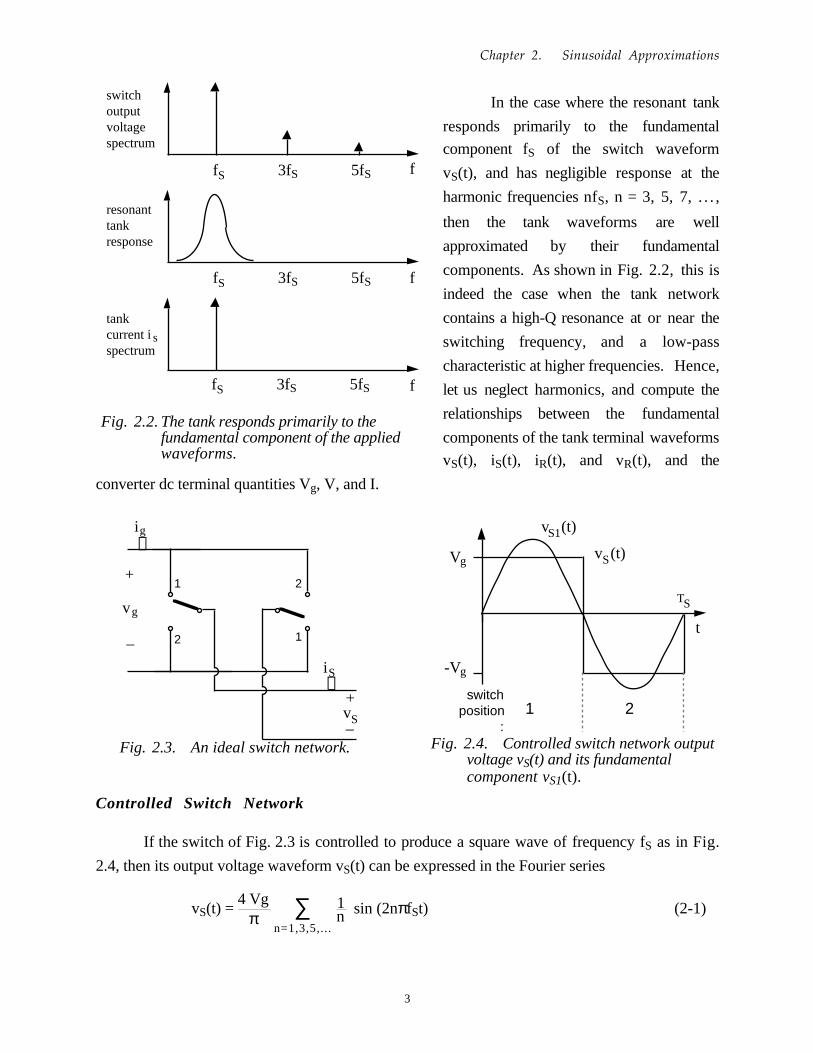
Fig. 2.1. A class of resonant converters which consist of cascaded switch, tank,rectifier, and filter networks. A series resonant converter example isshown.
In the most common modes of operation, the controlled switch network produces a square wave
voltage output vS(t) whose frequency fS is close to the tank network resonant frequency f0. In
response, the tank network rings with approximately sinusoidal waveforms of frequency fS. The
tank output waveform vR or iR is then rectified by network NR and filtered by network NF, to
produce the dc load voltage V and current I. By changing the switching frequency fS (closer to or
farther from resonance f0), the magnitude of the tank ringing response can be modified, and hence
the dc output voltage can be controlled.
Chapter 2. Sinusoidal Approximations
3
In the case where the resonant tank
responds primarily to the fundamental
component fS of the switch waveform
vS(t), and has negligible response at the
harmonic frequencies nfS, n = 3, 5, 7, . . . ,
then the tank waveforms are well
approximated by their fundamental
components. As shown in Fig. 2.2, this is
indeed the case when the tank network
contains a high-Q resonance at or near the
switching frequency, and a low-pass
characteristic at higher frequencies. Hence,
let us neglect harmonics, and compute the
relationships between the fundamental
components of the tank terminal waveforms
vS(t), iS(t), iR(t), and vR(t), and the
converter dc terminal quantities Vg, V, and I.
Controlled Switch Network
If the switch of Fig. 2.3 is controlled to produce a square wave of frequency fS as in Fig.
2.4, then its output voltage waveform vS(t) can be expressed in the Fourier series
vS(t) = 4 Vg
π ∑n=1,3,5,...
1n sin (2nπfSt) (2-1)
switchoutputvoltagespectrum
resonanttankresponse
f 3f 5f S S S
f 3f 5f S S S
f
f
f
tank current ispectrum
s
f 3f 5f S S S
Fig. 2.2.The tank responds primarily to thefundamental component of the appliedwaveforms.
1
2 1
2+
–
→
→
+
–vS
iS
i
gv
g
Fig. 2.3. An ideal switch network.
t
switchposition
:1 2
v (t)S1
v (t)S
TS
Vg
-Vg
Fig. 2.4. Controlled switch network outputvoltage vS(t) and its fundamentalcomponent vS1(t).

Principles of Resonant Power Conversion
4
The fundamental component is
vS1(t) = 4 Vg
π sin (2π fSt) (2-2)
which has a peak amplitude of (4/π) times the dc input voltage Vg, and is in phase with the original
square wave vS(t). Hence, the switch network output terminal is modeled as a sinusoidal voltage
generator, vS1(t).
It is interesting to model the converter dc input. This requires computation of the dc
component Ig of the switch input current ig(t). The switch input current ig(t) is equal to the output
current iS(t) when the switches are in position 1, and its inverse -iS(t) when the switches are in
position 2. Under the conditions described above, the tank rings sinusoidally and iS(t) is well
approximated by a sinusoid of some peak amplitude IS1 and phase ϕS:
iS(t) ≅ IS1 sin (2πfSt – ϕS) (2-3)
The input current waveform is shown in Fig. 2.5.
The dc component, or average value, of the
input current can be found by averaging ig(t) over
one half switching period:
ig = 2TS
ig(t)dt0
TS/2
≅ 2TS
IS1 sin (2πfSt - ϕS ) dt 0
TS/2
= 2π IS1 cos ϕS (2-4)
Thus, the dc component of the converter input
current depends directly on the peak amplitude of the tank input current IS1 and on the cosine of its
phase shift ϕS.
An equivalent circuit for the switch is given in Fig. 2.6. This circuit models the basic
energy conversion properties of the switch: the dc power supplied by the voltage source Vg is
converted into ac power at the switch output. Note that the dc power at the source is Vg times the
dc component of ig(t), and the ac power at the switch is the average of vS(t) times iS(t).
Furthermore, if the harmonics of vS(t) are negligible, then the switch output voltage can be
represented by its fundamental, a sinusoid vS1(t) of peak amplitude 4Vg/π.
i (t)S
ω tS
ϕS
i (t)g
Fig. 2.5.Switch terminal currentwaveforms ig(t) and iS(t).
Chapter 2. Sinusoidal Approximations
5
v (t) = sin(2πf t)
→
+
–
I cos(ϕ )S2__π S1 +
– SS1
i (t) ≅ Ι sin(2πf t − ϕ )S1S1 SS
_____4Vπ
g
ig
vg
Fig. 2.6. An equivalent circuit for the switch network which models thefundamental component of the output voltage waveform and the dccomponent of the input current waveform.
Uncontrolled rectifier with capacitive filter network
In the series resonant converter, the output rectifier is driven by the (nearly sinusoidal) tank
output current iR(t) and a large capacitor CF is placed at the dc output, so that the output voltage V
contains negligible harmonics of the switching frequency fS, as shown in Fig. 2.8. The diode
rectifiers switch when iR(t) passes through zero, as shown in Fig. 2.7, and the rectifier input
voltage vR(t) is essentially a square wave, equal to +V when iR(t) is positive and -V when iR(t) is
negative. Note that vR(t) is in phase with iR(t).
If the tank output current iR(t) is a sinusoid with peak amplitude IR1 and phase shift ϕR:
iR(t) = IR1 sin (2πfSt - ϕR) (2-5)
then the rectifier input voltage may be expressed in the Fourier series
vR(t) = 4Vπ
∑n=1,3,5,...
1n sin (2πnfS t – ϕR) (2-6)
where ϕR is the phase shift of iR(t). This voltage waveform is impressed on the output terminal of
the resonant tank network. Again, if the tank network responds primarily to the fundamental
component of fS of vR(t), and has negligible response at the harmonic frequencies nfS, n =
Ri (t)
ϕR
vR(t)+V
–V
IR1
ω tS
Fig. 2.7 Rectifier input waveforms iR(t)and vR(t).
R
+ V –
I→
loadlow passfilter
uncontrolledrectifier
→||iR(t)||
→iR(t)
+
vR(t)
–
D5
D6
D7
D8
Fig 2.8 Uncontrolled rectifier withcapacitive filter network, as in the seriesresonant converter. The diodes switchwhen iR(t) passes through zero.

Principles of Resonant Power Conversion
6
3,5,7..., then the harmonics of vR(t) can be ignored. vR(t) is then well approximated by its
fundamental component vR(t):
vR1(t) = 4Vπ
sin (2π fSt – ϕR) (2-7)
The fundamental voltage component vR1(t) has a peak value of (4/π) times the dc output voltage
V, and it is in phase with the current iR(t).
The rectified tank output current, | iR(t) |, is filtered by capacitor CF. Since no dc current
can pass through CF, the dc component of | iR(t) | must be equal to the steady-state load current I.
Equating dc components yields:
I = 2TS
IR1 | sin (2π fSt - ϕR) | dt
0
TS/2
= 2
π IR1 (2-8)
Therefore, the load current and the tank output current amplitudes are directly related in steady-
state.
Since vR1(t), the fundamental component of vR(t), is in phase with iR(t), the rectifier
presents an effective resistive load Re to the tank circuit. The value of Re is equal to the ratio of
vR1(t) to iR(t). Division of Eq. (2-7) by Eq. (2-5), and elimination of IR1 using Eq. (2-8) yields
Re = vR1(t)iR(t)
= 8π2
VI
(2-9)
With a resistive load, R = V/I, this equation reduces to
Re = 8π2
R = 0.8106 R (2-10)
Thus, the tank network is damped by an effective load resistance Re equal to 81% of the actual load
resistance R. An equivalent circuit is given in Fig. 2.9.
+ V –
I→
R↑π2 IR1
→+
vR1(t) –
iR(t) = IR1sin(2πf t - ϕ )S
R = Rπ___8
2e
T
Fig. 2.9. An equivalent circuit for the uncontrolled rectifier with capacitive filternetwork, which models the fundamental components of the tankoutput waveforms iR(t) and vR1(t), and the dc components of the loadwaveforms I and V. The rectifier presents an effective resistive loadRe to the tank network.

Chapter 2. Sinusoidal Approximations
7
Resonant tank network
We have postulated that the effects of harmonics can be neglected, and we have
consequently shown that the bridge behaves like a fundamental voltage source vS1(t) and that the
rectifier behaves like a resistor of value Re. We can now solve the resonant tank network by
standard linear analysis.
As shown in Fig. 2-10, the tank circuit is a
linear network with the voltage transfer function:
vR1(s)vS1(s)
= H(s) (2-11)
Hence, the ratio of the peak magnitudes of vR1(t)
and vS1(t) is given by:
peak magnitude of vR1(t)peak magnitude of vS1(t)
= || H(s) ||s=j 2π fs(2-12)
In addition, iR is given by:
iR(s) = vR1(s)
Re =
H(s)Re
vS1(s) (2-13)
So the peak magnitude of iR is:
IR1 = || H(s) ||S = j2πfS
Re ⋅ (peak magnitude of vS1(t)) (2-14)
Solution of converter voltage conversion ratio V/Vg
An equivalent circuit of a complete resonant converter is depicted in Fig. 2.11. The
complete voltage conversion ratio of the resonant converter can now be found:
|vR1||)
(s)||s=
}
V||iR||
VVg
= (R) (2π) ⋅ 1
Re( )⋅
⋅( I ) ( ) ⋅||iR||
|| ||( )
}} }
R1vI
j2πfs)4π( )
⋅ (|| v S1||Vg
)
}
⋅⋅ ( ||He
(|||v ||S1
(2-15)
Simplification by use of Eq. (2-10) yields the final result:
vS1
iR1
+–
tanknetwork
+
vR1 –
⇒Z
S1i
Re
H( )S
i
Fig. 2.10. The linear tank network, excitedby an effective sinusoidal input sourceand driving an effective resistive load.

Principles of Resonant Power Conversion
8
VVg
= || H(s) ||s=j 2π fs (2-16)
Eq. (2-16) is the desired result. It states that the dc conversion ratio of the resonant
converter is approximately the same as the ac transfer function of the resonant tank circuit,
evaluated at the switching frequency fS. This intuitive result can be applied to converters with
many different types of tank circuits. However, it should be re-emphasized that Eq. (2-16) is valid
only if the response of the tank circuit to the harmonics of vS(t) is negligible compared to the
fundamental response, an assumption which is not always valid. In addition, we have assumed
that the switch network is controlled to produce a square wave and that the rectifier network drives
a capacitive-type network. Finally, the transfer function H(s) is evaluated assuming that the load,
Re, is effectively resistive, and it is given by Eq. (2-10).
R→ 2π
||iR1||{ {
H( )S
tanknetwork
Zi⇒
+–
iR1
+
vR1 –
R
R = R___82π
4V_____π
sin(2πf t)SvS1 =
vS1
iS1
→
2__π
||i || cos(ϕ )S1 Si =
controlled rectifier with dc input switch ac tank network capacitive filter dc output
gg
vg
ig
e
e+-
Fig. 2.11. Steady-state equivalent circuit which models the dc andfundamental components of resonant converter waveforms.
Converter efficiency
The effects of tank component losses can also be easily estimated using the model of Fig.
2.11. The converter input power is
Pin = Vg Ig = Vg 2π ||iS|| cos ϕS
(2-17)
Note that ||iS|| cos ϕS is equal to the real part of iS(s). In addition, iS(s) is equal to the switch output
voltage vS1(s) divided by the tank input impedance Zi(s):
iS(s) = vS1(s)Zi(s)
= Yi(s) vS1(s) (2-18)
Hence, the real part of iS(s) is:

Chapter 2. Sinusoidal Approximations
9
Real(iS(s)) = ||vS1(s)|| Real(Yi(s)) = 4Vg
π ⋅ Real(Yi (s))
(2-19)
and the input power is:
Pin = 8π2
Vg2 Real(Yi(s)) (2-20)
The converter output power is:
Pout = IV = ||vR1||
2
2 Re(2-21)
But vR1(s) = vS1(s) H(s), and hence ||vR1||2 = ||vS1(s)||2 ||H(s)||2. So
Pout = ||vS1(s)||2 ||H(s)||2
2 Re =
π2Vg2
8R ||H(s)||2
(2-22)
Hence, the converter efficiency is:
η = PoutPin
= ||H(s)||2
Re⋅Real(Yi(s))(2-23)
This expression models the losses associated with the tank network in a simple, circuit-oriented
way. Tank network efficiency can be estimated by computing the tank transfer function H(s) and
the tank input admittance Yi(s), and then evaluating Eq. (2-23). An example is given in the
following section, in which the influence of tank inductor core loss and capacitor esr on converter
efficiency is determined.
2 . 2 . Series Resonant Converter Example
The series resonant converter with switching frequency control is shown in Fig. 2.1. For
this circuit, the tank network consists of a series L-C circuit, and Fig. 2.11 can be redrawn as in
Fig. 2.12.
The transfer function H(s) is therefore:
H(s) = ReZi(s)
= Re
Re + sL + 1sC
=
sQeω0
1 + sQeω0
+ sω0
2 (2-24)
+–
iR1
+
vR1 –
L CiS1
⇒ZvS1 R
ie
Fig. 2.12.Equivalent circuit which modelsthe fundamental components of the tankwaveforms in the series resonantconverter.
Principles of Resonant Power Conversion
10
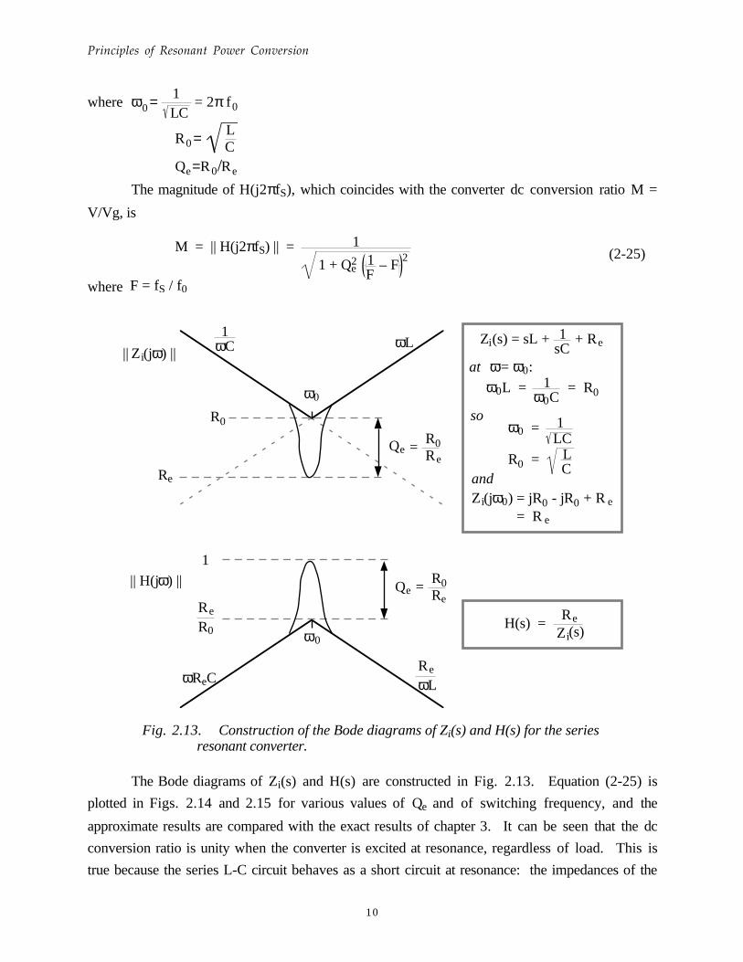
where ω0= 1LC
= 2π f 0
R0= LC
Qe=R0/Re
The magnitude of H(j2πfS), which coincides with the converter dc conversion ratio M =
V/Vg, is
M = || H(j2πfS) || = 1
1 + Qe2 1
F – F
2 (2-25)
where F = fS / f0
1ωC ωL
ω0
R0
|| Z (jω) ||Z (s) = sL + 1
sC + R
ω0L = 1ω0C
= R0
so ω0 = 1
LC
R0 = LC
andZ (jω0) = jR0 - jR0 + R
= R
at = 0:
= R0R
Q
R
ωL
ω0R0
1
|| H(jω) || = R0R
Q
R
RωR C
H(s) = R
Z (s)
i
i
i
e
ee
e
e
e
e
ee
e
e
e
i
ωω
Fig. 2.13. Construction of the Bode diagrams of Zi(s) and H(s) for the seriesresonant converter.
The Bode diagrams of Zi(s) and H(s) are constructed in Fig. 2.13. Equation (2-25) is
plotted in Figs. 2.14 and 2.15 for various values of Qe and of switching frequency, and the
approximate results are compared with the exact results of chapter 3. It can be seen that the dc
conversion ratio is unity when the converter is excited at resonance, regardless of load. This is
true because the series L-C circuit behaves as a short circuit at resonance: the impedances of the

Chapter 2. Sinusoidal Approximations
11
tank inductor and capacitor are equal in magnitude but opposite in phase, and their sum is zero.
The voltages vS and vR are therefore the same. It can also be seen that a decrease in the load
resistance R, which increases the effective quality factor Qe, causes a more peaked response in the
vicinity of resonance.
0.5 0.6 0.7 0.8 0.9 1.0
0.0
0.2
0.4
0.6
0.8
1.0
exact M, Q=2approx M, Q=2exact M, Q=10approx M, Q=10exact M, Q=0.5approx M, Q=0.5
F
M =
V/V
g
Fig. 2.14. Comparison of exact and approximate series resonant convertercharacteristics, below resonance.
1 2 3 4 5
0.0
0.2
0.4
0.6
0.8
1.0
exact M, Q=0.5approx M, Q=0.5exact M, Q=10approx M, Q=10exact M, Q=2approx M, Q=2
F
M=V
/Vg
Fig. 2.15. Comparison of approximate and exact series resonant convertercharacteristics, above resonance.
Over what range of switching frequencies is Eq. (2-25) accurate? The response of the tank
to the fundamental component of vS(t) must be sufficiently greater than the response to the

Principles of Resonant Power Conversion
12
harmonics of vS(t). This is certainly true for operation above resonance because H(s) contains a
bandpass characteristic which decreases with a single pole slope for fS > f0. For the same reason,
Eq. (2-25) is valid when the switching frequency is below but near resonance.
However, for switching frequencies fS much less than the resonant frequency f0, the
sinusoidal approximation breaks down completely because the tank responds more strongly to the
harmonics of vS(t) than to its fundamental. For example, at fS = f0/3, the third harmonic of vS(t) is
equal to f0 and directly excites the tank resonance. Some other type of analysis must be used to
understand what happens at these lower frequencies. Also, in the low-Q case, the approximation
is less accurate because the filter response is less peaked, and hence does not favor the fundamental
component as strongly. As shown in a later chapter, discontinuous conduction modes may then
occur whose waveforms are highly non sinusoidal.
Efficiency
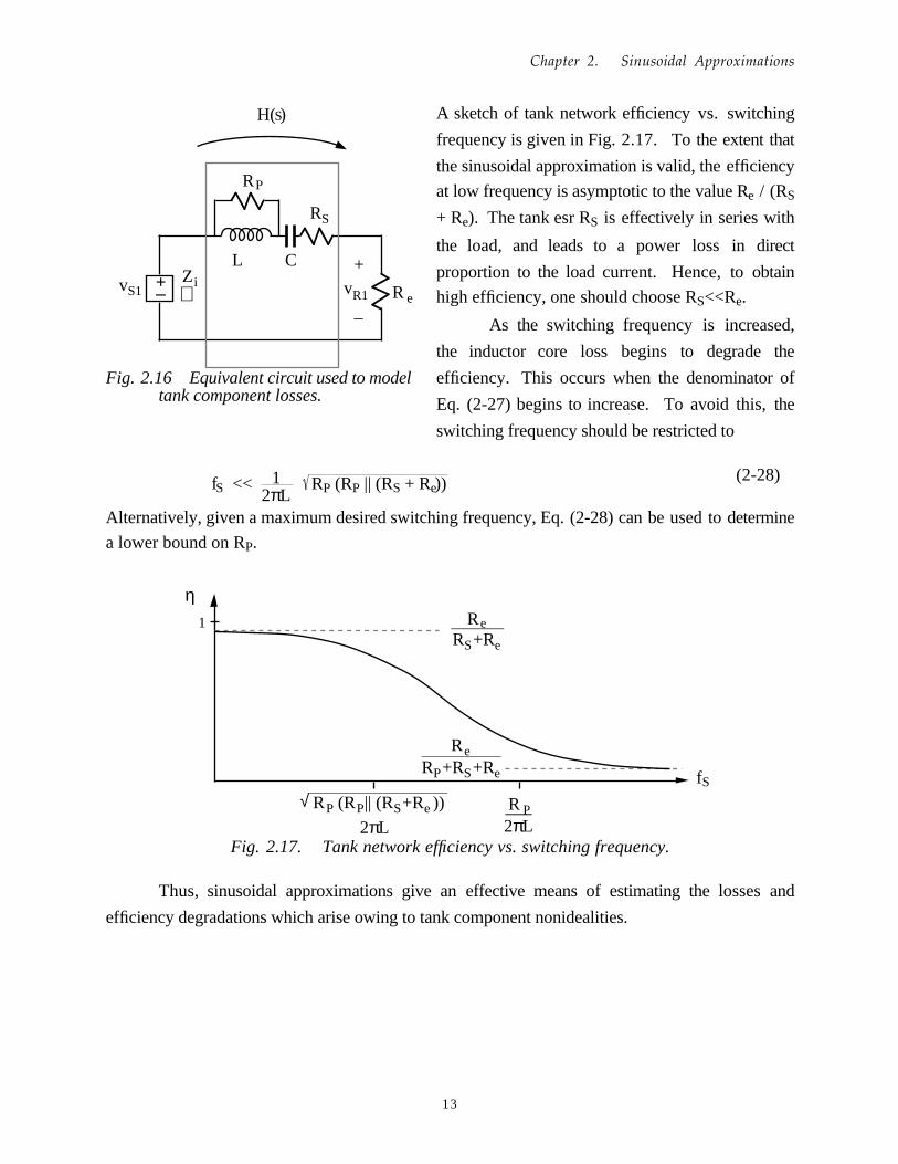
A similar analysis can be used to compute the converter efficiency. Let us model the effects
of tank inductor core loss by a resistance RP, and tank inductor winding resistance and tank
capacitor equivalent series resistance (esr) by an effective resistance RS, as shown in Fig. 2.16.
Standard circuit analysis can be used to show that the tank transfer function H(s) is given
by
H(s) =
sωe
1 + sωp
1 + sQeω0
+ sω0
2 (2-26)
whereω0 = 1
LC RP+RS+ReRP
ωe = 1ReC
ωP = RPL
1Qe
= R0RP
+ Re + RSR0
R0 = LC
⋅ 1 + RS + ReRP
The efficiency is found by evaluation of Eq. (2-23). For the circuit of Fig. 2.16, the efficiency is:
η = ReRS + Re
(1 + (2πL
RP)2 fS2)
(1 + (2πL)2
RP (RP || (RS + Re)) fS
2) (2-27)
Chapter 2. Sinusoidal Approximations
13
A sketch of tank network efficiency vs. switching
frequency is given in Fig. 2.17. To the extent that
the sinusoidal approximation is valid, the efficiency
at low frequency is asymptotic to the value Re / (RS
+ Re). The tank esr RS is effectively in series with
the load, and leads to a power loss in direct
proportion to the load current. Hence, to obtain
high efficiency, one should choose RS<<Re.
As the switching frequency is increased,
the inductor core loss begins to degrade the
efficiency. This occurs when the denominator of
Eq. (2-27) begins to increase. To avoid this, the
switching frequency should be restricted to
fS << 12πL
RP (RP || (RS + Re))(2-28)
Alternatively, given a maximum desired switching frequency, Eq. (2-28) can be used to determine
a lower bound on RP.
______________________
1
ηR
R +RS e
________
R +R +RP S e
____________Re
fS
R (R || (R +R ))P P S e
_____________________√
2πLR___P2πL
e
Fig. 2.17. Tank network efficiency vs. switching frequency.
Thus, sinusoidal approximations give an effective means of estimating the losses and
efficiency degradations which arise owing to tank component nonidealities.
+
vR1
–⇒+
–
L C
R
RS
RP
ZvS1 ei
H( )S
Fig. 2.16 Equivalent circuit used to modeltank component losses.

Principles of Resonant Power Conversion
14
2 . 3 . Subharmonic Modes of the Series Resonant Converter
If the nth harmonic of the switch output
waveform vS(t) is close to the resonant tank
frequency, nfS ~ f0, and if the tank effective quality
factor Qe is sufficiently large, then as shown in
Fig. 2.18, the tank responds primarily to harmonic
n. All other components of the tank waveforms
can then be neglected, and it is a good
approximation to replace vS(t) with its nth harmonic
component:
vS(t) ≅ vSn(t) = 4 Vgnπ TS
sin (nωSt) (2-29)
This differs from Eq. (2-2) because the amplitude is reduced by a factor of 1/n, and the frequency
is nfS rather than fS.
f
switchoutputvoltagespectrum
f
f
f 3f 5fSSS
f 3 f 5fSSS
f 3 f 5fSSS
resonanttankresponse
tankcurrent ispectrum
s
Fig 2.18 When the tank responds primarilyto the third harmonic of the switchingfrequency, then frequency componentsother than the third harmonic may beneglected.

Chapter 2. Sinusoidal Approximations
15
f0 fs13 f0
M1
13
15 f0
15
Fig. 2.19 The subharmonic modes of the series resonant converter. These modes occurwhen the harmonics of the switching frequency excite the tank resonance.
The arguments used to model the tank and rectifier/filter networks are unchanged from
section 2.1. The rectifier presents an effective resistive load to the tank, of value Re = 8R/π2. In
consequence, the converter dc conversion ratio is given by
M = VVg
= || H (j2πnfS) ||
n (2-30)
This is a good approximation provided that nfS is close to f0, i.e.,
(n-1) fS < f0 < (n+1) fS (2-31)
and Qe is sufficiently large. Typical characteristics are plotted in Fig. 2.19.
The series resonant converter is not generally designed to operate in a subharmonic mode,
since the fundamental modes yield greater output voltage and power, and hence higher efficiency.
Nonetheless, the system designer should be aware of their existence, because inadvertent operation
in these modes can lead to large signal instabilities.
2 . 4 . The Parallel Resonant Converter
The parallel resonant converter is diagrammed in Fig. 2.20. It differs from the series
resonant converter in two ways. First, the tank capacitor appears in parallel with the rectifier
network rather than in series: this causes the tank transfer function H(s) to have a different form.
Second, the rectifier drives an inductive-input low-pass filter. In consequence, the value of the
effective resistance Re differs from that of the rectifier with a capacitive filter. Nonetheless,
sinusoidal approximations can be used to understand the operation of the parallel resonant
converter.

Principles of Resonant Power Conversion
16
+–
→
controlledswitch
network
powerinput
NS
I→
R
loadlow passfilter
resonanttank
network
NT
uncontrolledrectifier
NR NF
→iR+
vR –
+ V –
+
–
→i S
i (t)
v
vS
g
g
Fig. 2.20. Block diagram of the parallel resonant converter.
As in the series resonant converter, the switch network is controlled to produce a square
wave vS(t). If the tank network responds primarily to the fundamental component of vS(t), then
arguments identical to those of section 2.1 can be used to model the output fundamental
components and input dc components of the switch waveforms. The resulting equivalent circuit is
identical to Fig. 2.6.
The uncontrolled rectifier with inductive filter network can be described using the dual of
the arguments of Section 2.1. In the parallel resonant converter, the output rectifiers are driven by
the (nearly sinusoidal) tank capacitor voltage vR(t), and the diode rectifiers switch when vR(t)
passes through zero as in Fig. 2.21. The rectifier input current iR(t) is therefore a square wave of
amplitude I, and it is in phase with the tank capacitor voltage vR(t).
The fundamental component of iR(t) is
iR1(t) = 4 Iπ
sin (2πfSt - ϕR) (2-32)
Hence, the rectifier again presents an effective
resistive load to the tank circuit, equal to
Re = vR1(t)iR1(t)
= πVR14 I (2-33)
The ac components of the rectified tank
capacitor voltage | vR(t) | are removed by the
output low pass filter. In steady state, the
output voltage V is equal to the dc component of | vR(t) |:
V = 2TS
VR1 | sin (2πfSt - ϕR) | dt
0
TS
2(2-34)
So the load voltage V and the tank capacitor voltage amplitude are directly related in steady state.
Substitution of Eq. (2-27) and resistive load characteristics V = IR into Eq. (2-26) yields:
Ri (t)
ϕR
vR(t)
+I
–I
VR1
ω tS
Fig. 2.21. Parallel resonant converterwaveforms vR(t) and iR(t).

Chapter 2. Sinusoidal Approximations
17
Re = π2
8 R = 1.2337 R (2-35)
An equivalent circuit for the uncontrolled
rectifier with inductive filter network is given in Fig.
2.22. This model is similar to the one used for the
series resonant converter, Fig. 2.9, except that the
roles of the rectifier input voltage vR and current iR are
interchanged, and the effective resistance Re has a
different value. The model for the complete converter
is given in Fig. 2.23.
Solution of Fig. 2.23 yields the converter dc
conversion ratio:M = V
Vg = 8
π2 || H(s) ||s=j2πfs (2-36)
where H(s) is the tank transfer function
H(s) = Z0(s)sL (2-37)
and Z0(s) = sL || 1sC
|| Re (2-38)
4V____π
g
= sin(2πf t)
tanknetwork
H(s)
{ {
+–
→
+
–
vR(t)
→iR1(t)
R+–vS1
S1i
⇒Z R = Rπ2__
8
I→
+
–
V R1
2π V=
S v (t) = V sin(2πf t - ϕ )R RR1 S
controlled rectifier withdc input switch ac tank network inductive filter dc output
i g
vg ie
+-
π= ||i ||cos(ϕ )2S1 Sig vS1
Fig. 2.23. Equivalent circuit for the parallel resonant converter, whichmodels the fundamental components of the tank waveforms, and thedc components of the input current and output voltage.
→I→
+–
+
–
vR(t)
iR1(t)
R = __π2
8 R
–
v (t) = V sin(2πf t - ϕ )RR1R S
e
+ V
= R12π V
Fig. 2.22. An equivalent circuit for therectifier with inductive output filter,which models the fundamentalcomponent of the ac side voltage,and the dc component of the dc sidevoltage, in the parallel resonantconverter.

Principles of Resonant Power Conversion
18
ω0
1
C____1
2Lω
|| ||H(j )ω
Qe
RR0
____e
ω0
R
R
Q =RR0
___
LC
___1
|| ||Z (j )0
ωω
ω
ee
e
0
jR R R___ ___ ___
ω0L = 1ω0C
= R0
so ω0 = 1
LC
R = 0LC
and
:
Z (s)0= sL || || R1
sC
Z (j )0
=
=
1
1 j 1
0 0
0
e
__________________
e
Re
ω
= 0ω ωat
H(s) = Z (s)0
sL_______
+ +
Fig. 2.24.Construction of Bode diagrams of Zi(s) and H(s) for the parallel resonant converter.
The Bode magnitude diagrams of H(s) and Z0(s) are constructed in Fig. 2.24. Z0(s) is the
parallel combination of the impedance of the tank inductor L, capacitor C, and effective load Re.
The magnitude asymptote of the parallel combination of these components, at a given frequency, is
equal to the smallest of the individual asymptotes ωL, 1/ωC, and Re. Hence, at low frequency
where the inductor impedance dominates the parallel combination, || Z0(s) || ≅ ωL, while at high
frequency the capacitor dominates and || Z0(s) || ≅ 1/ωC. At resonance, the impedances of the
inductor and capacitor are equal in magnitude but opposite in phase, so that their effects cancel.
|| Z0 || is then equal to Re:
|| Z0(s) ||s=j ω0 = 1
1jω0L
+ jω0C + 1Re
= Re (2-39)
where ω0L = 1ω0C
= R0
The dc conversion ratio is therefore

Chapter 2. Sinusoidal Approximations
19
M = 8π2
|| 1
1 + sQeω0
+ ( sω0
)2 ||s=j2πfs
= 8π2
⋅ 1
(1 - F2)2 + (FQe
)2(2-40)
Equation (2-40) is compared with the exact converter solution in Fig. 2.25.
0.50 1.00 1.50 2.00 2.50 3.00
0.00
0.50
1.00
1.50
2.00
2.50
3.00
M
F
Qe=5
Qe=2
Qe=1
Qe=0.5
Qe=0.2
Fig. 2.25. Comparison of exact parallel resonant converter characteristics(solid lines) vs. the approximate solution, Eq. (2-40) (shaded lines).
Principles of Resonant Power Conversion
20
2 . 5 . Switching at Zero Current or Zero Voltage
Operation of the Full Bridge Below Resonance
An advantage of resonant
converters is their reduced switching loss.
When the series resonant converter is
operated below resonance, a phenomenon
known as “zero current switching” can
occur, in which the transistors naturally
switch off at zero current. With a simple
circuit modification, the transistor turn-on
transition can also be caused to occur at
zero current. Let us consider the operation
of the full bridge switch in more detail.
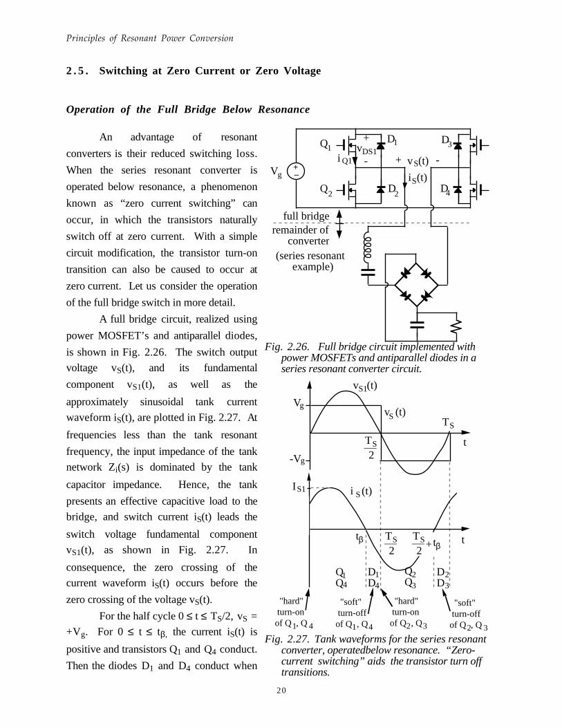
A full bridge circuit, realized using
power MOSFET’s and antiparallel diodes,
is shown in Fig. 2.26. The switch output
voltage vS(t), and its fundamental
component vS1(t), as well as the
approximately sinusoidal tank current
waveform iS(t), are plotted in Fig. 2.27. At
frequencies less than the tank resonant
frequency, the input impedance of the tank
network Zi(s) is dominated by the tank
capacitor impedance. Hence, the tank
presents an effective capacitive load to the
bridge, and switch current iS(t) leads the
switch voltage fundamental component
vS1(t), as shown in Fig. 2.27. In
consequence, the zero crossing of the
current waveform iS(t) occurs before the
zero crossing of the voltage vS(t).
For the half cycle 0 ≤ t ≤ TS/2, vS =
+Vg. For 0 ≤ t ≤ tβ, the current iS(t) is
positive and transistors Q1 and Q4 conduct.
Then the diodes D1 and D4 conduct when
D1 D3
D4
full bridgeremainder of
converter(series resonant example)
i (t)S
+ -v (t)S
Q1
D2Q2
i Q1
+
-vDS1
+–Vg
Fig. 2.26. Full bridge circuit implemented withpower MOSFETs and antiparallel diodes in aseries resonant converter circuit.
TS___2
v (t)S
v (t)S1
Vg
-Vg
TS
TS___2
t
t
i (t)SI S1
"hard" turn-onof Q , Q1 4
"soft" turn-offof Q , Q1 4
"hard" turn-onof Q , Q2 3
"soft" turn-offof Q , Q2 3
DD
DD
1 14 4
23
23
tβ TS___2
+tβ
Fig. 2.27.Tank waveforms for the series resonantconverter, operatedbelow resonance. “Zero-current switching” aids the transistor turn offtransitions.

Chapter 2. Sinusoidal Approximations
21
iS(t) is negative, tβ ≤ t ≤ TS/2. The situation
during TS/2 ≤ t ≤ TS is symmetrical. Since iS1
leads vS1, the transistors conduct before their
respective antiparallel diodes. Note that, at anygiven time during the D1 conduction interval tβ
≤ t ≤ TS/2, transistor Q1 can be turned off
without incurring switching loss. The circuit
naturally causes the transistor turn off transition
to be lossless, and long turn off switching
times can be tolerated.
In general, “zero current switching” can
occur when the resonant tank presents an
effective capacitive load to the switches, and
the switch current zero crossings occur before
the switch voltage zero crossings. In the
bridge configuration, zero current switching is
characterized by the conduction sequence Q1-
D1-Q2-D2, such that the transistors are turned
off while their respective antiparallel diodes conduct. It is possible, if desired, to replace the
transistors with naturally-commutated thyristors whenever the zero-current-switching property
occurs.
The transistor turn on transition
in Fig. 2.28 is similar to that of a PWM
switch, and it is not lossless. During
the turn on transition of Q1, diode D2
must turn off. Neither the transistor
current nor the transistor voltage is
zero, Q1 passes through a period of
high instantaneous power dissipation,
and switching loss occurs. As in the
PWM case, the reverse recovery current
of diode D2 flows through Q1. This
current spike can be the largest
component of switching loss. In
addition, the energy stored in the drain-
to-source capacitances of Q1 and Q2
i Q1
Q1 D1
Q2D2
+
-vDS1
remainderof converter
i (t)S
+ -v (t)S
i D2
Lleg
Lleg
D3
D4
Q3
Q4
Lleg
Lleg
+–Vg
Fig. 2.29 Addition of small inductors Lleg, whicheffectively snub the transistor turn-on transition andreduce turn-on switching loss in the SRC operatedbelow resonance.
TSTS___2
t
i (t)SI S1
vDS1
Vg
soft turn-off
hard turn-on:current spike
due to D stored charge
2
TS___2
tTS0
DD
DD
1 14 4
23
23
tβTS___+ tβ2
Fig. 2.28. Tank waveforms for the seriesresonant converter, operated belowresonance. “Zero-current switching” aidsthe transistor turn off transitions.

Principles of Resonant Power Conversion
22
and in the depletion layer capacitance of
D1 is lost when Q1 turns on.
To assist the transistor turn on
process, small inductors are often
introduced into the legs of the bridge
(Fig. 2.29). During the normal Q1, D1,
Q2, and D2 conduction intervals, these
inductors appear in series with the tank
inductor L, and hence the effective total
tank inductance is
Leffective = L + 2Lleg (2-41)
In addition, these leg inductors
introduce commutation intervals at
transistor turn on. At the instant when
Q1 is turned on, the tank current
flowing through diode D2 begins to
shift to Q1, at a rate determined by Vg
and 2Lleg. The transistor current
magnitude is therefore limited by Lleg,
rather than being determined by the
stored charge in diode D2. During time
tδ,
tδ = 2 Lleg iS(0)
Vg(2-42)
where iS(0) is the tank current at the
beginning of the commutation interval,
the current in diode D2 reaches zero,
and D2 turns off. The leg inductance
Lleg is chosen such that tδ is longer than
the gate-driver-limited MOSFET turn-
on time, but is much shorter than normal Q1, D1, Q2, and D2 conduction intervals. Thus, the
MOSFET is switched fully on before the drain current rises significantly above zero, and nearly
lossless snubbing at turn-on occurs. This lossless snubbing of the diode D2 stored charge during
the Q1 turn-on transition is probably the most common reason to use zero current switching.
A nonideality not considered in the discussion above is the effect of other semiconductor
device capacitances. Transistor Q1 output capacitance, diode D1 junction capacitance, and diode
D1 stored charge can be modeled as effective parallel capacitances which are shorted out whenever
v (t)S
v (t)S1
Vg
-Vg
TSTS___2
t
t α t
iD2(t)
iQ1(t)
iS1(t)
turn-oncommutationinterval
tδ
Fig. 2.30. Waveforms for the circuit of Fig. 2.29.During time tδ, the tank current commutes from D2to Q1.

Chapter 2. Sinusoidal Approximations
23
transistor Q1 is turned on. In consequence, switching loss occurs equal to the total stored energy
in these capacitances times the switching frequency. Similar switching losses occur in the other
three legs of the bridge. This loss mechanism, while not as great as the loss owing to the stored
charge in D2, can nonetheless be quite significant in converters operating from high input voltages
and at high switching frequencies. It is often a significant disadvantage of zero current switching
schemes.
Operation of the Full Bridge Above Resonance
When the series resonant converter
is operated above resonance, a different
phenomenon known as “zero voltage
switching” can occur, in which the
transistors naturally switch on at zero
voltage. With a simple circuit modification,
the transistor turn-off transition can also be
caused to occur at zero voltage. Ideally,
this process is the dual of the “zero current
switching” process described in the
previous section.
For the full bridge circuit of Fig.
2.26, the switch output voltage vS(t), and
its fundamental component vS1(t), as well
as the approximately sinusoidal tank current
waveform iS(t), are plotted in Fig. 2.31. At
frequencies greater than the tank resonant
frequency, the input impedance of the tank
network Zi(s) is dominated by the tank
inductor impedance. Hence, the tank
presents an effective inductive load to the
bridge, and the switch current iS(t) lags the
switch voltage fundamental component
vS1(t), as shown in Fig. 2.31. In
consequence, the zero crossing of the
voltage waveform vS(t) occurs before the
current waveform iS(t).
v (t)S
v (t)S1
Vg
-Vg
TSTS___2
t α
t
t
"soft" turn-onof Q , Q1 4 1 4
"hard" turn-offof Q , Q
DD
DD
1144
23
23
iS1(t)
Fig. 2.31.Tank waveforms for the series resonantconverter, operated above resonance. “Zerovoltage switching” aids the transistor turn-ontransitions.

Principles of Resonant Power Conversion
24
For the half cycle 0 ≤ t ≤ TS/2, vS =
+Vg. For 0 ≤ t ≤ tα, the current iS(t) is
positive and the transistors Q1 and Q4
conduct, and the diodes D1 and D4 conduct
when iS(t) is negative, tα ≤ t ≤ TS/2. The
situation during TS/2 ≤ t ≤ TS is
symmetrical. Since vS1 leads iS1, the
transistors conduct after their respective
antiparallel diodes. Note that, at any given
time during the D1 conduction interval 0 ≤ t
≤ tα, transistor Q1 can be turned on without
incurring switching loss. The circuit
naturally causes the transistor turn-on
transition to be lossless, and long turn-on
switching times can be tolerated.
In general, “zero voltage switching”
can occur when the resonant tank presents
an effective inductive load to the switches, and hence the switch voltage zero crossings occur
before the switch current zero crossings. In the bridge configuration, zero voltage switching is
characterized by the conduction sequence D1-Q1-D2-Q2, such that the transistors are turned on
while their respective antiparallel diodes conduct. Since the transistor voltage is zero during the
entire turn on transition, switching loss due to slow turn-on times or due to energy storage in any
of the device capacitances does not occur at turn-on.
The transistor turn-off transition in Fig. 2.32 is similar to that of a PWM switch, and is not
lossless. During the turn-off transition of Q1, diode D2 must turn on. Neither the transistor
current nor the transistor voltage is zero, Q1
passes through a period of high instantaneous
power dissipation, and switching loss occurs.
To assist the transistor turn off process,
small capacitors may be introduced into the legs
of the bridge, as demonstrated in Fig. 2.33.
Alternatively, the existing device capacitances
can be used. A delay is also introduced into the
gate drive signals, so that there is a short
commutation interval when all four transistors
are off. During the normal Q1, D1, Q2, and D2
conduction intervals, the leg capacitors appear
vDS1
Vg
tTS TS 2
TS 2TS
iQ1 soft turn-on
hardturn-off
t
Fig. 2.32.Detail of Q1 drain current and drain-source voltage waveforms, SRC example,operation above resonance.
Q1
Q2 D2
D1
remainder of converter
i (t)S
+ -v (t)SVg
Cleg
Cleg
va
Q
Q3
4
D3
D4
Cleg
Cleg
+–
Fig. 2.33. Introduction of small capacitors Cleg,which effectively snub the transistor turn-offt ransition and can reduce turn-off switchingloss in the SRC operated above resonance.

Chapter 2. Sinusoidal Approximations
25
in parallel with the semiconductor switches, and have no effect on the converter operation.
However, these capacitors introduce commutation intervals at transistor turn-off. When Q1 is
turned off, the tank current iL(TS/2) flows through the switch capacitances Cleg instead of Q1, and
the voltage across Q1 and Cleg increases. Eventually, the voltage across Q1 reaches Vg; diode D2
then becomes forward-biased. The length of this commutation interval is:
tδ = 2 Cleg Vg
iL(TS/2)` (2-43)
where iL(TS/2) is the tank current at the beginning of the commutation interval, the voltage reaches
zero, and D2 becomes forward-biased. The leg capacitance Cleg is chosen such that tδ is longer
than the gate-driver-limited MOSFET turn-off time, but is much shorter than normal Q1, D1, Q2,
and D2 conduction intervals. Thus, the MOSFET is switched fully off before the drain voltage
rises significantly above zero, and nearly lossless snubbing at turn-off occurs. The fact that none
of the semiconductor device capacitances or stored charges lead to switching loss is the major
advantage of zero-voltage switching, and is the most common motivation for its use.
An additional advantage is the
reduction of EMI associated with device
capacitances. In conventional PWM
converters and, to a lesser extent, in zero-
current switching converters, significant
high frequency ringing and current spikes
are generated by the rapid charging and
discharging of the semiconductor device
capacitances at turn on and/or turn off.
Converters in which all semiconductor
devices switch at zero voltage inherently do
not generate this type of EMI.
A nonideality not considered in the
discussion above is the effect of
semiconductor package inductances. These
inductances are open-circuited whenever
the semiconductor device is turned off. In
consequence, switching loss occurs equal
to the total stored energy in these
inductances times the switching frequency.
This loss mechanism can be significant in
converters operating with high currents and
low input voltages and at high switching frequencies.
t
t
t
tα
conducting devices:
commutation interval
t δ
X XDD
14
1
423
DD
23
1DD4
+Vg
-Vg
vS1(t)
vS(t)
TS2
TS
is1(t)
va(t)
Fig. 2.34. Waveforms for the circuit of Fig.2.33. During the commutation interval tδ , allsemiconductor devices are in the off state, andthe tank circuit is(t) charges or discharges thecapacitors, Cleg.

Principles of Resonant Power Conversion
26
REFERENCES
[1] R.L. Steigerwald, “A Comparison of Half-Bridge Resonant Converter Topologies,” IEEE Applied PowerElectronics Conference, 1987 Proceedings, pp. 135-144, March 1987.
[2] R. Severns, “Topologies for Three Element Resonant Converters,” IEEE Applied Power ElectronicsConference, 1990 Proceedings, pp. 712-722, March 1990.
PROBLEMS
1 . Analysis of the LCC converter
LVg
V+
–
LF
CF
I
R
+–
C1C2
The “LCC” converter shown above contains both series and parallel tank capacitors.
a) Using the sinusoidal approximation method, find an expression for the dc conversion ratio M of thisconverter.
b) For large C1, the circuit becomes essentially a parallel resonant converter with added blocking capacitor C1.
Use the approximate factorization method to approximate the tank transfer function H(s) for this case.Show that your result of part (a) reduces to the parallel resonant converter M, with an added rolloff (invertedpole) for low switching frequencies due to C1. Identify a resonant frequency and Q for this case, and sketch
typical curves of M vs. F for a few values of Q>1.
c) Use the approximate factorization method to approximate the tank transfer function H(s) for large C2. For
this case, the resonance occurs at approximately
f0 = 1
2π LC1
What is the Q?
d) For the case when C1 = C2 = C, sketch typical ||H(s)|| asymptotes for the high Q case, i.e., Re >> R0 where
R0 = L2C
Identify salient features.

Chapter 2. Sinusoidal Approximations
27
2 . Dual of the series resonant converter
LC+
–Vg
LF1
LF2
CF
Ig→
iR(t)→
I→
R
→iS(t)
→
+ vC(t) –
iL(t)
+
vF1(t)
–
f0 = 12π LC
LF1, LF2, and CF are large filter elements, whose switching ripples are small. L and C are tank elements,whose waveforms iL and vC are nearly sinusoidal.
a) Using the sinusoidal approximation method, develop equivalent circuit models for the switch network, tanknetwork, and rectifier network.
b) Sketch a Bode diagram of the parallel LC parallel tank impedance.
c) Solve your model. Find an analytical solution for the converter voltage conversion ratio M = V/Vg, as afunction of the effective Qe and the normalized switching frequency F = fs/f0. Sketch M vs. F.
d) What can you say about the validity of the sinusoidal approximation for this converter? Which parts of yourM vs. F plot of part (c) are valid and accurate?
e) Below resonance, does the converter operate with zero-voltage switching or with zero-current switching?What about above resonance?