terials - srm institute of science and technology unit...terials absorption of light by molecules...
TRANSCRIPT

Pro
perties o
f Nan
om
aterials
PHOTOCHEMISTRY
Pro
perties o
f Nan
om
aterials
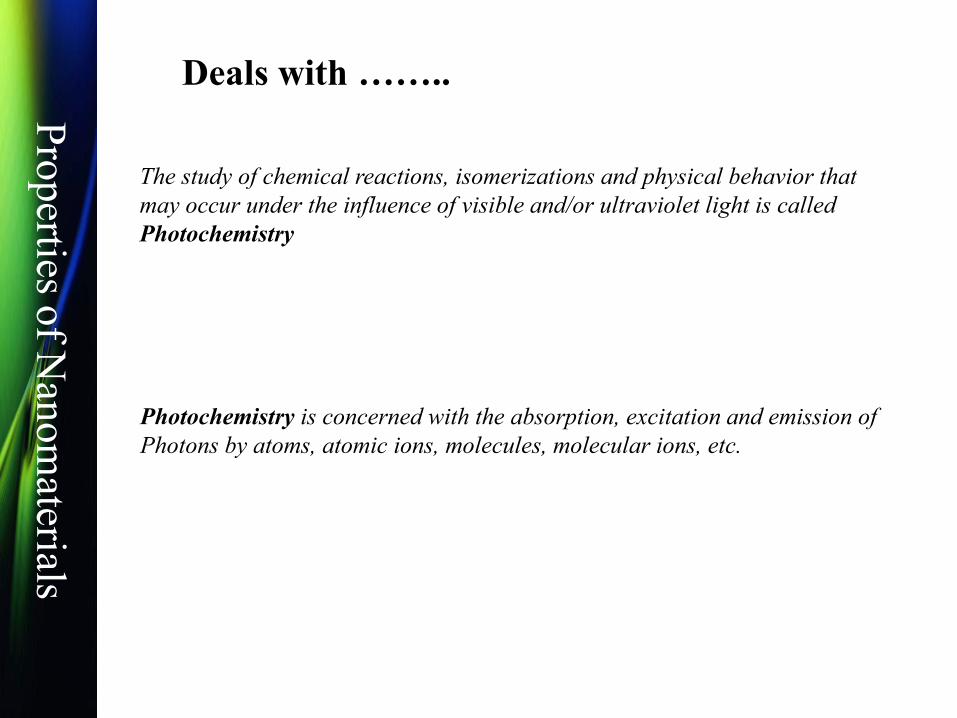
The study of chemical reactions, isomerizations and physical behavior that
may occur under the influence of visible and/or ultraviolet light is called
Photochemistry
Photochemistry is concerned with the absorption, excitation and emission of
Photons by atoms, atomic ions, molecules, molecular ions, etc.
Deals with ……..

Pro
perties o
f Nan
om
aterials
Processes involved when molecule absorbs light
Processes involved after the molecule absorbs light
Rates ands efficiencies photochemical processes
Deals with ……..

Pro
perties o
f Nan
om
aterials
Two fundamental principles
The first law of photochemistry
(Grotthuss-Draper law)
Light must be absorbed by a compound in order for a
photochemical reaction to take place
The second law of photochemistry
(Stark-Einstein law)
Also known as "photo-equivalence law“ It states that
for each photon of light absorbed by a chemical
system, only one molecule is activated for
subsequent reaction
For each photon of light absorbed by a chemical
system, only one molecule is activated for a
photochemical reaction
1 mol of photons is called Einstien

Pro
perties o
f Nan
om
aterials
The simplest photochemical process is seen with the absorption and
subsequent emission of a photon by a gas phase atom such as sodium.
When the sodium atom absorbs a photon it is said to be excited. After
a short period of time, the excited state sodium atom emits a photon
of 589 nm light and falls back to the ground state:

Pro
perties o
f Nan
om
aterials
The Electromagnetic Spectrum
Photons have an energy which is dependent upon the wavelength of the
light. The rule is:
Long wavelength light = low energy
Short wavelength light = high energy
Absorption of light : Bohr’s rule
Absorption Photons of frequency will only occur if the molecule has
two energy levels, Ei and Ef such that
Ef- Ei = h

Pro
perties o
f Nan
om
aterials
Absorption of light by molecules
When a molecule absorbs a photon it is promoted to a higher energy
state –an excited state- that may have excess electronic , vibrational or
rotational energy depending on the energy of the Photon
Electronic energy which involves the molecule having electrons
in different orbitals
Vibrational Energy in which the atoms of the molecule are
vibrating
Rotational levels, in which molecule may be rotating at different
speeds
Each of these energies quantized meaning only certain values are
allowed.
The allowed values are different for different molecules

Pro
perties o
f Nan
om
aterials
In photochemical reactions involving visible and UV
light , the energy levels involved are usually electronic
energy levels
Vibrational energy level transition are in the infra red
Rotational Energy transitions are in the microwave region
A useful way of remembering photochemically active region:
Wavelength in the range 200-600 nm

Pro
perties o
f Nan
om
aterials
Absorption of light : Selection rules
Pro
perties o
f Nan
om
aterials
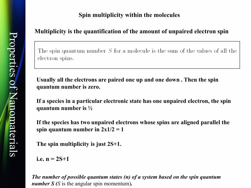
Multiplicity is the quantification of the amount of unpaired electron spin
Usually all the electrons are paired one up and one down . Then the spin
quantum number is zero.
If a species in a particular electronic state has one unpaired electron, the spin
quantum number is ½
If the species has two unpaired electrons whose spins are aligned parallel the
spin quantum number in 2x1/2 = 1
The spin multiplicity is just 2S+1.
i.e. n = 2S+1
The number of possible quantum states (n) of a system based on the spin quantum
number S (S is the angular spin momentum).
Spin multiplicity within the molecules

Pro
perties o
f Nan
om
aterials

Pro
perties o
f Nan
om
aterials
Electronic Levels
(Dark Lines)
Vibrational Levels
(Light Lines)
First Excited State
Ground State
Energy Levels

Pro
perties o
f Nan
om
aterials
Absorption of a photon and thus excitation to
S1 or S2 respectively
Radiationless energy loss to return to S1
Reconversion to S0 to S1 with emission of
radiation –fluroscence
Transition between Levels

Pro
perties o
f Nan
om
aterials
Fluorescence

Pro
perties o
f Nan
om
aterials
Kasha’s-rule
The emission of the fluorescence light is always starting from the lowest vibrational level of the first
excited level (S1).
Jablonski (1898-1980)
excitation (10-15s)
Internal conversion or vibrational relaxation – heat (10-12s)
internal conversion = heat (10-7 – 10-5 s)
S1 – S0 (10-8s) -
fluorescence
Kasha-rule
Jablonski diagram
The Jablonski diagram describes most of the relaxation mechanisms for excited state
molecules

Pro
perties o
f Nan
om
aterials
Fluorescence
• A type of luminescence
– Length (lifetime): ~10-8s (~10ns)
– Singlet – singlet transition.

Pro
perties o
f Nan
om
aterials
Phosphorescence

Pro
perties o
f Nan
om
aterials
Internal conversion (IC) where the electron relaxes to the ground state with no radiation. The
molecule transfers to a high vibrational level of the ground state and then loses the
vibrational energy through non-radiative decay via collisions with solvent.
Intersystem crossing (ISC) where the molecules transfer to a triplet state by flipping an electron
spin. The triplet state then undergoes non-radiative decay and ultimately phosphoresces

Pro
perties o
f Nan
om
aterials
Phosphorescence
• A type of photo-luminescence.
–Time-scale: ~10-3 – 10-1s (~ms - s)
–Singlet - triplet - singlet transition

Pro
perties o
f Nan
om
aterials
As shown on the Jablonski diagram above, the lowest triplet state, T1, is nearly always below S1
therefore the phosphorescence emission is significantly red-shifted (lower energy) than
fluorescence.

Pro
perties o
f Nan
om
aterials
Fluorescent minerals emit visible light when exposed to
ultraviolet light
Pro
perties o
f Nan
om
aterials
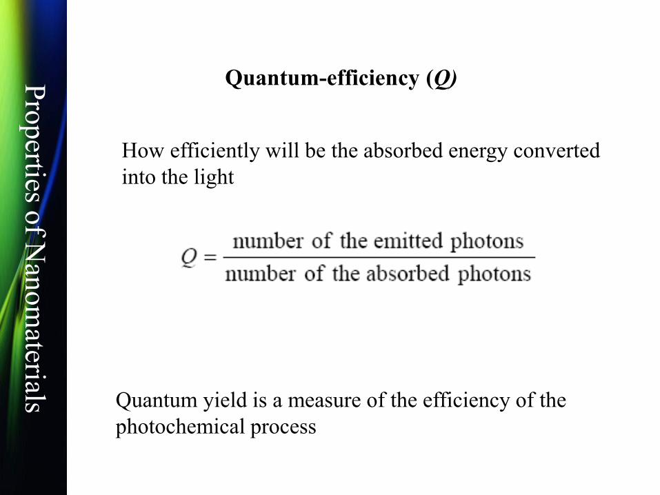
Quantum-efficiency (Q)
How efficiently will be the absorbed energy converted
into the light
Quantum yield is a measure of the efficiency of the
photochemical process

Pro
perties o
f Nan
om
aterials
Fluorescence lifetime (τ)
The average length of the excited state of
a fluorophore before emitting a photon.

Pro
perties o
f Nan
om
aterials
Light can be absorbed and re-emitted by matter, and this is
called luminescence.
There are two types of luminescence: Fluorescence and
Phosphorescence.
Fluorescence is the process of absorbing and re-emitting
light on a timescale of about 10-8 seconds
Phosphorescence processes are much slower, taking about
10-3 to 1 second to occur (even longer lifetimes are possible)
Luminescence

Pro
perties o
f Nan
om
aterials
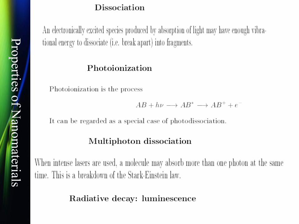
What happens after absorption ?
Radiation loss
Intramolecular Energy Transfer
Intermolecular Energy Transfer
Isomerization
Dissociation
Ionization
Chemical Reaction

Pro
perties o
f Nan
om
aterials
In chemistry isomerisation is the process by which one molecule is
transformed into another molecule which has exactly the same atoms,
but the atoms are rearranged e.g. A-B-C → B-A-C

Pro
perties o
f Nan
om
aterials
Pro
perties o
f Nan
om
aterials

Pro
perties o
f Nan
om
aterials

Pro
perties o
f Nan
om
aterials

Pro
perties o
f Nan
om
aterials

Pro
perties o
f Nan
om
aterials
ELECTROCHEMISTRY OF
NANOMATERIALS

Pro
perties o
f Nan
om
aterials
Electrochemistry involves chemical phenomena
associated with charge separation.
Often this charge separation leads to charge transfer,
which can occur homogeneously in solution, or
heterogeneously on electrode surfaces.

Pro
perties o
f Nan
om
aterials
Electrochemistry is the study of phenomena at
electrode-solution interfaces

Pro
perties o
f Nan
om
aterials
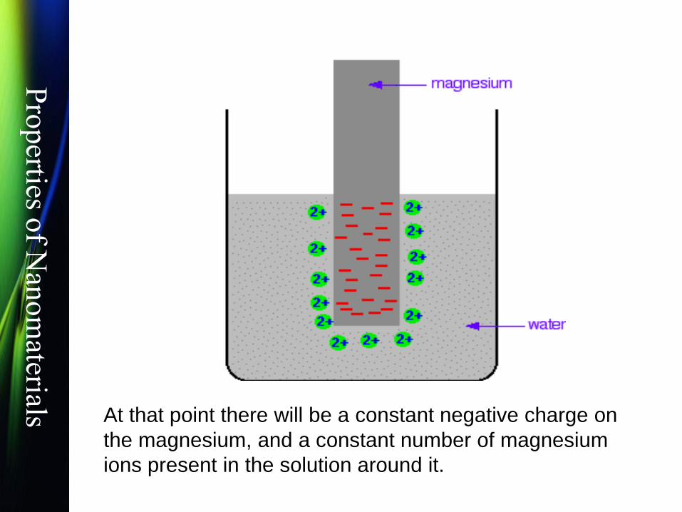
Looking at this from an equilibrium point of
view
Suppose you have a piece
of magnesium in a beaker
of water. There will be
some tendency for the
magnesium atoms to shed
electrons and go into
solution as magnesium ions.
The electrons will be left
behind on the magnesium.

Pro
perties o
f Nan
om
aterials A dynamic equilibrium will be established when the rate at which
ions are leaving the surface is exactly equal to the rate at which
they are joining it again.
Pro
perties o
f Nan
om
aterials At that point there will be a constant negative charge on
the magnesium, and a constant number of magnesium
ions present in the solution around it.

Pro
perties o
f Nan
om
aterials
Copper is less reactive and so forms its ions less readily. Any
ions which do break away are more likely to reclaim their
electrons and stick back on to the metal again. You will still
reach an equilibrium position, but there will be less charge on
the metal, and fewer ions in solution.

Pro
perties o
f Nan
om
aterials
Obviously, the voltmeter will show that the zinc is the negative
electrode, and copper is the (relatively) positive one.

Pro
perties o
f Nan
om
aterials
(a) Galvanic and (b) electrolytic cells
Pro
perties o
f Nan
om
aterials
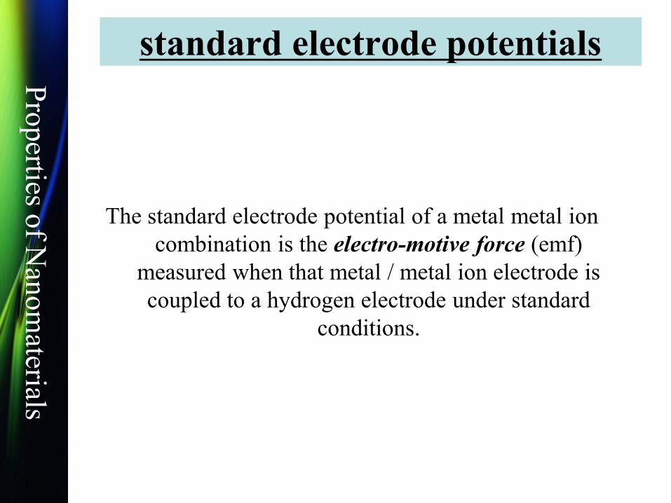
standard electrode potentials
The standard electrode potential of a metal metal ion
combination is the electro-motive force (emf)
measured when that metal / metal ion electrode is
coupled to a hydrogen electrode under standard
conditions.

Pro
perties o
f Nan
om
aterials
Magnesium has a much greater tendency to form its ions than
hydrogen does. The position of the magnesium equilibrium will
be well to the left of that of the hydrogen equilibrium.
That means that there will be a much greater build-up of
electrons on the piece of magnesium than on the platinum.

Pro
perties o
f Nan
om
aterials
What if you replace the magnesium half
cell by a copper one?

Pro
perties o
f Nan
om
aterials
The two equilibria which are set up in the half cells are:
Pro
perties o
f Nan
om
aterials
The overall chemical reaction taking place in a cell is made up of two independent half-reactions, which describe the real chemical changes at the two electrodes.
Most of the time one is interested in only one of these reactions, and the electrode at which it occurs is called the working (or indicator) electrode, coupled with an electrode that approaches an ideal nonpolarizable electrode of known potential, called the reference electrode. In experiments, the current is passed between the working electrode and an auxiliary(or counter) electrode.
Three electrodes are frequently placed in three compartments separated by a sintered-glass disk.
Reactions and electrodes

Pro
perties o
f Nan
om
aterials
Reference electrode:
A reference electrode is used in measuring the working
electrode potential of an electrochemical cell.
The reference electrode acts as a reference point for the
redox couple.

Pro
perties o
f Nan
om
aterials
working electrode
A fixed potential difference is applied between the working electrode and the reference electrode.
This potential drives the electrochemical reaction at the working electrode's surface.
The current produced from the electrochemical reaction at the working electrode is balanced by a current flowing in the opposite direction at the counter
electrode.

Pro
perties o
f Nan
om
aterials
Electrode reactions are heterogeneous and take place in the interfacial region between electrode and solution diffusion layer
The charge separation at each electrode is represented by a capacitance
the difficulty of charge transfer by a resistance
The electrode can act as (1) a source of electrons (cathode) reduction ,(2) a sink of electrons transferred from species in solution (anode) oxidation
The amount of electrons transferred is related to the current flowing between the two electrodes
The nature of electrode reactions

Pro
perties o
f Nan
om
aterials
Methods for studying electrode reactions
steady state methods
Linear sweep methods: increasing sweep rate
Step and pulse techniques
Impedance methods
The type of technique chosen will depend very much on the timescale of
the electrode reaction

Pro
perties o
f Nan
om
aterials
Applications
Once electrode reactions and electrode processes are understood, this
knowledge can be used for:
Tailoring electrode reactions
Studying complex systems in which many electrode reactions occur
simultaneously
Measuring concentrations of electroactive species
electroplating, batteries, fuel cells,
electrochemical machining, and many other
related applications, including minimization of
corrosion; biosensors, etc

Pro
perties o
f Nan
om
aterials
Syntheses of Nanomaterials by
Electrodeposition
Pro
perties o
f Nan
om
aterials
52
What is electrodeposition?
Definition: the process that exploits the creation of solid materials directly from
electrochemical reactions in liquid compositions with substrate materials.
One of the chemical methods; Also known as electroplating.
Two technologies for plating:
Electroplating: Substrate is placed in electrolyte. When an electrical
potential is applied between a conducting area on the substrate and a
counter electrode in the liquid, a chemical redox process takes place
resulting in the formation of a layer of material on the substrate and usually
some gas generation at the counter electrode.
Electroless plating: Substrate is placed in a more complex chemical
solution, in which deposition happens spontaneously on any surface which
forms a sufficiently high electrochemical potential with the solution. No
external electrical potential and contact to the substrate are required, but
more difficult to control the thickness and uniformity of the deposits.

Pro
perties o
f Nan
om
aterials
53
Bulk electrodeposition: slow and leads to low-grade materials
Template-assisted/mold-guided electrodeposition
Arrays of nanostructured materials with specific arrangements
Employing either an active or restrictive template as a cathode in an
electrochemical cell
Important technique for synthesizing metallic nanomaterials with
controlled shape and size
Limitations
Typically restricted to electrically conductive substrate materials
Difficulties in the preparation of desired templates.
Additional high temperature annealing steps are expensive and
unsuitable for polymer substrates
Electroplating

Pro
perties o
f Nan
om
aterials
54
Traditional Experimental Setup
A three-electrode electrochemical cell (a reference electrode, a specially
designed cathode, and an anode or counter electrode)
Accessories for applying controlled current at a certain voltage (dc or Ac
power supply or potential stat)
The template can be made of either nonmetallic or metallic materials
The surface morphology of the deposits depends on the surface structure and
chemical composition of the cathode substrate as well as other
electrochemical parameters.

Pro
perties o
f Nan
om
aterials
55
Thermodynamic and Kinetics of Electrodeposition
The nucleation of nanostructures on the electrode substrate is influenced by the
crystal structure of the substrate, specific free surface energy, adhesion
energy, lattice orientation of the electrode surface, and crystallographic lattice
mismatch at the nucleus-substrate interface boundary.
The final size distribution of the electrodeposits strongly depends on the
kinetics of the nucleation and growth:
Instantaneous nucleation: all the nuclei form instantaneously on the
electrode substrate, and subsequently grow with the time of
electrodeposition.
Progressive nucleation: the number of nuclei that are formed is a function
of time of electrodeposition. These nuclei gradually grow and overlap, and
therefore, the progressive nucleation process exhibits zones of reduced
nucleation rate around the growing stable nuclei.
Pro
perties o
f Nan
om
aterials
56
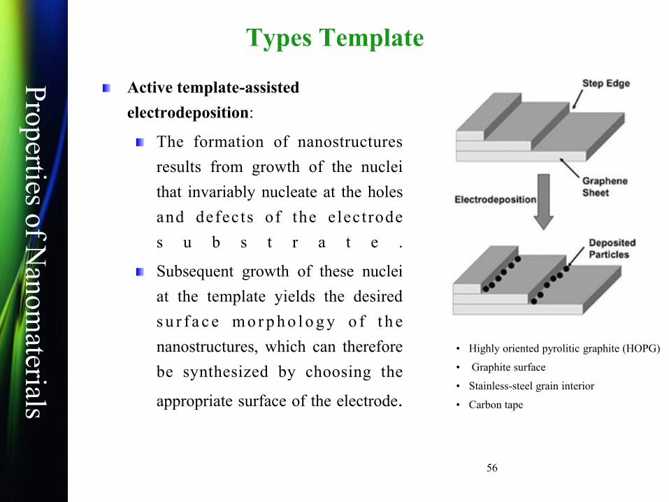
Types Template
Active template-assisted
electrodeposition:
The formation of nanostructures
results from growth of the nuclei
that invariably nucleate at the holes
and defects of the e lectrode
s u b s t r a t e .
Subsequent growth of these nuclei
at the template yields the desired
s u r f a c e m o r p h o l o g y o f t h e
nanostructures, which can therefore
be synthesized by choosing the
appropriate surface of the electrode.
• Highly oriented pyrolitic graphite (HOPG)
• Graphite surface
• Stainless-steel grain interior
• Carbon tape

Pro
perties o
f Nan
om
aterials
57
Types of Template
Restrictive Template-Based
Electrodeposition
It involves the deposition of metal into
the cylindrical pores or channels of an
inert, nonconductive nanoporous
substrate.
To prepare nanometer-sized particles,
fibrils/wires, rods, and tubules.
Examples: nanoindented holes;
nanoporous polymers; porous alumina

Pro
perties o
f Nan
om
aterials
58
Local electrodeposition by scanning electrochemical microscope
The currents are established between a
microelectrode and the surface of a
conducting substrate placed close to it (e.g.
tenths of micron).
The electrochemical processes on the
substrate surface are localized to a region
which size is very similar to that of the
microelectrode.
Co microelectrode has been oxidized in a
controlled way very close to the surface of a
Au substrate. The Co microelectrode works
like a source of Co2+ ions. The substrate
potential is also controlled for every ion to
be reduced (deposited). The amount of
cobalt deposited in a substrate region
depends on how long the process is held.
(a) metallic ion free electrolyte
(b) electrolyte with Cl¯

Pro
perties o
f Nan
om
aterials
59
Versatile technique to synthesize various kinds of nanomaterials with
desired surface morphologies (nanorods, nanoparticles, and nanowires).
The major problem with using electrodeposition to synthesize
nanostructure is the preparation of proper templates/substrate.
Electrodeposition is highly influenced by the surface characteristics of
the electrode substrate, and the shape and size of the deposits depend on
the substrate.
Further studies on the fundamentals of the nucleation and growth of
nanostructure are needed to understand the preferential deposition on a
particular site of the electrode substrate
It can be scaled down to the deposition of a few atoms or up to
large dimensions

Pro
perties o
f Nan
om
aterials
Nanometer-scale cuprous oxide (colorized red)
can be electrodeposited through the openings in
the hexagonally packed intermediate layer
protein (white regions) from the bacterium
Deinococcus radiodurans. Purified crystalline
protein sheets are first adsorbed to a conductive
substrate, and then electrodeposition is carried
out to fill the nanometer-scale pores in the
protein.
Nanobiosystems:Biological fabrication

Pro
perties o
f Nan
om
aterials
PHOTOCONDUCTIVITY
Pro
perties o
f Nan
om
aterials
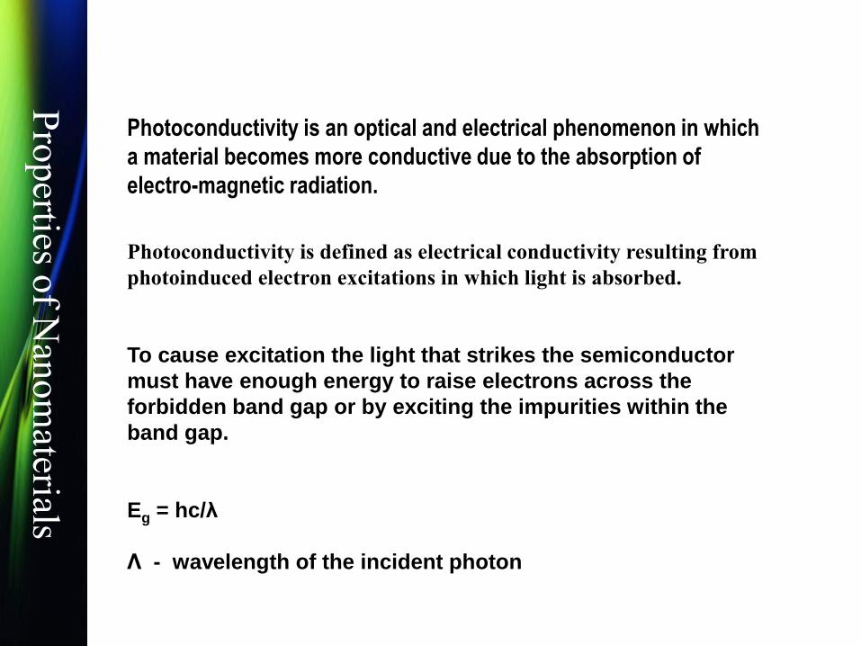
Photoconductivity is an optical and electrical phenomenon in which
a material becomes more conductive due to the absorption of
electro-magnetic radiation.
Photoconductivity is defined as electrical conductivity resulting from
photoinduced electron excitations in which light is absorbed.
To cause excitation the light that strikes the semiconductor
must have enough energy to raise electrons across the
forbidden band gap or by exciting the impurities within the
band gap.
Eg = hc/λ
Λ - wavelength of the incident photon

Pro
perties o
f Nan
om
aterials
Impurities and imperfections can also contribute
towards photoconductivity.
If these are present in the material, then even the
photos having energy below the threshold for the
production of electron hole pairs may be able to
produce mobile electron –holes.
Impurities and imperfection introduce discrete energy
levels in the forbidden energy gap called traps.

Pro
perties o
f Nan
om
aterials
Conductivity
σ = n e μe (Ω–m)–1
where n is the number of electrons in the conduction band,
e is the charge of the electrons, and μe is the electron mobility.
For these electrons to reach the conduction band, the
semiconductor must have a sufficiently narrow enough band
gap.
Quantum efficiency of the absorption process is the ratio of
number of photons absorbed per second to number of photons
incident per second

Pro
perties o
f Nan
om
aterials
Spectral response
Variation of photoconductivity with
photon energy is known as spectral
response. The maximum value of
photocurrents corresponds to the band
gap energy.
Speed of response
The rate of change of photoconductivity
with the change in the photo excitation
intensity. It is studied by switching off a
steady photo excitation which is
followed by the decay of photo
excitation.

Pro
perties o
f Nan
om
aterials
Dark Resistance
As the name implies, the dark resistance is the resistance of the
cell under zero illumination lighting conditions.
In some applications this can be very important since the dark
resistance defines what maximum “leakage current” can be
expected when a given voltage is applied across the cell. Too
high a leakage current could lead to false triggering in some
applications.

Pro
perties o
f Nan
om
aterials
Gold electrode contacts made across a
CdS nanowire through electron beam
lithography.
CdS is a wide-band gap semiconductor (Eg = 2.4 eV), which puts the excitation
wavelength at 517 nm.

Pro
perties o
f Nan
om
aterials Current-over-time graph used to measure the photoresponse of the
CdS nanowires to visible light
Pro
perties o
f Nan
om
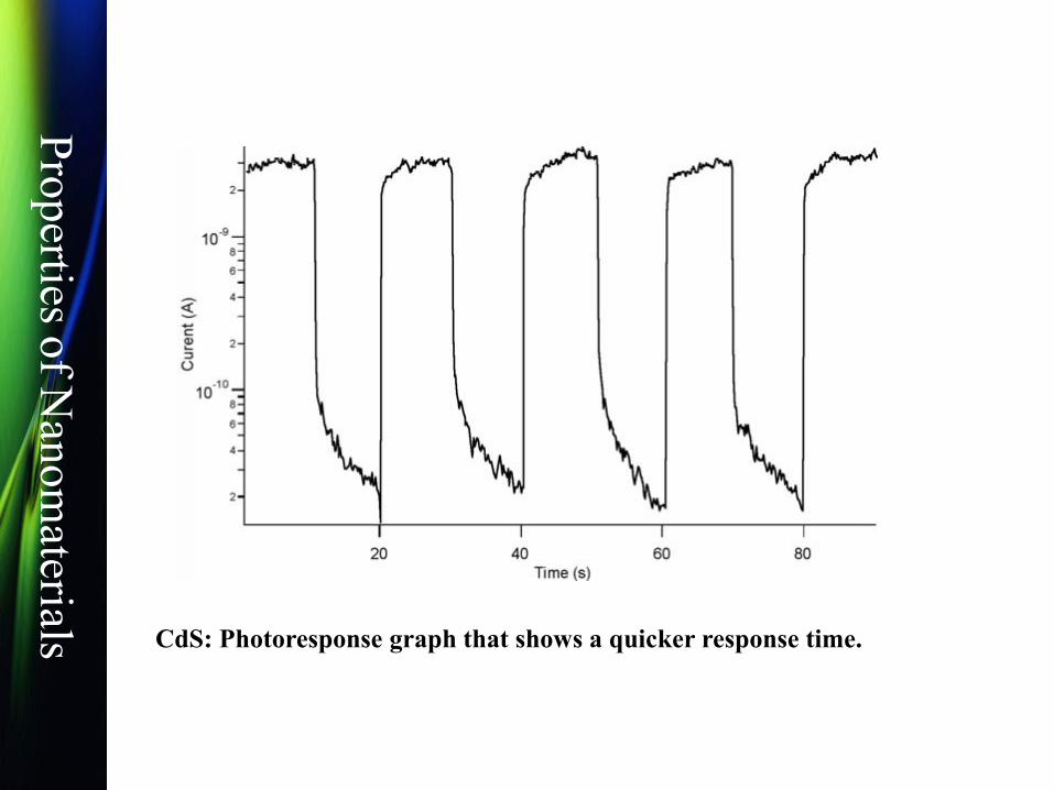
aterials CdS: Photoresponse graph that shows a quicker response time.

Pro
perties o
f Nan
om
aterials
CdS :Current vs. intensity graph that measures the current response to
varying light intensity.
From the data, CdS nanowires have been shown to have a significant
photoresponse in the presence of a light source. In particular, due to their wide
band gap, CdS nanowires are extremely sensitive to light in the visible range,
specifically to visible light in the green spectrum

Pro
perties o
f Nan
om
aterials
ZnO nanoparticles based photoconductive cell

Pro
perties o
f Nan
om
aterials
From the data, CdS nanowires have been shown to
have a significant photoresponse in the presence of a
light source.
In particular, due to their wide band gap, CdS
nanowires are extremely sensitive to light in the
visible range, specifically to visible light in the green
spectrum

Pro
perties o
f Nan
om
aterials
Photoconductivity measurements on ZnO nanoparticles
with a constant applied voltage V = 50 V

Pro
perties o
f Nan
om
aterials
Two factors are important for any application of ZnO for UV
detection:
the sensitivity (expressed in A cm2 W−1 or in A W−1),
the visible light rejection,
i.e. the ratio of the current in the UV spectrum compared to the
current in the visible spectrum. Since the current in the visible
spectrum is related to defects, a good crystalline structure is
required for a high visible rejection.
So far, sensitivities of 30 A W−1 have reported on ZnO thin films and
of 10−3 A cm2 W−1 on ZnO nanowires
Since ZnO gap energy lies in the ultraviolet (UV) range, ZnO is
suitable for UV detection by using its photoconduction properties

Pro
perties o
f Nan
om
aterials
Diffusion in Nanomaterials

Pro
perties o
f Nan
om
aterials
What is Diffusion?
Diffusion is material transport by atomic motion.
or
Movement of particles in a solid from an area of high
concentration to an area of low concentration, resulting
in the uniform distribution of the substance
Inhomogeneous materials can become
homogeneous by diffusion. For an active diffusion
to occur, the temperature should be high enough to
overcome energy barriers to atomic motion

Pro
perties o
f Nan
om
aterials
Diffusivity depends on
1.Diffusion mechanism
2. Temperature of diffusion
3. Type of crystal structure (bcc > fcc)
4. Crystal imperfections
5. Concentration of diffusing species

Pro
perties o
f Nan
om
aterials
ATOMIC MODELS OF DIFFUSION
Vacancy Mechanism
To jump from lattice site to lattice site, atoms need energy
to break bonds with neighbors, and to cause the necessary
lattice distortions during jump. This energy comes from the
thermal energy of atomic vibrations (Eav ~ kBT)
The direction of flow of atoms is opposite the vacancy
flow direction
Pro
perties o
f Nan
om
aterials
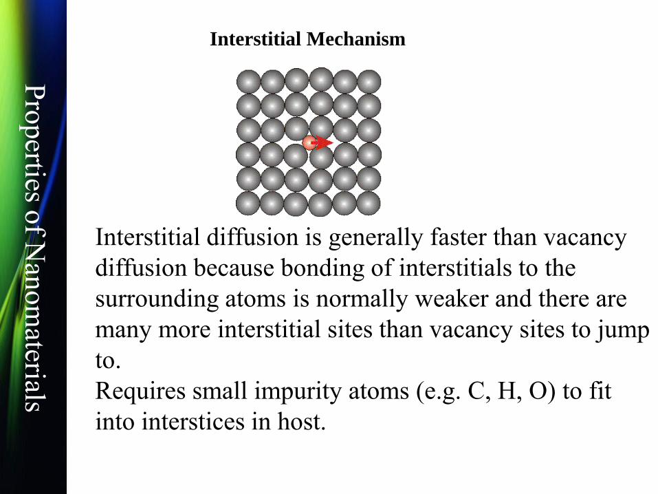
Interstitial diffusion is generally faster than vacancy
diffusion because bonding of interstitials to the
surrounding atoms is normally weaker and there are
many more interstitial sites than vacancy sites to jump
to.
Requires small impurity atoms (e.g. C, H, O) to fit
into interstices in host.
Interstitial Mechanism

Pro
perties o
f Nan
om
aterials
Diffusion is controlled by two laws defined by Ficks
Steady state diffusion: the diffusion flux does not change with time
Fick’s first law of diffusion
Concentration profile: concentration of atoms/molecules
of interest as function of position in the sample.

Pro
perties o
f Nan
om
aterials
The flux of diffusing atoms, J, is used to quantify
how fast diffusion occurs. The flux is defined as
either the number of atoms diffusing through unit
area per unit time (atoms/m2-second)
Diffusion Flux
dt
dn
AJ
1

Pro
perties o
f Nan
om
aterials
dx
dcDA
dt
dn
gradientionconcentrattimeareaatomsJ //
dx
dcJ
dx
dcDJ
dx
dcD
dt
dn
AJ
1
Fick‟s first law
Flux (J) → Flow / area / time [Atoms / m2 / s]

Pro
perties o
f Nan
om
aterials
Fick’s I law
dx
dcDA
dt
dn
No. of
atoms
crossing
area A
per unit
time
Cross-sectional area
Concentration gradient
Matter transport is down the concentration gradient
Diffusion coefficient/ diffusivity
A Flow direction
As a first approximation assume D f(t)

Pro
perties o
f Nan
om
aterials
Second Fick’s law of diffusion
In practice the concentration of solute atoms at any point in
the material changes with time – non-steady-state diffusion
The changes of the concentration profile can be described in
this case by a differential equation, Fick’s second law.
The rate of compositional change is equal to the diffusivity times
the rate of the change of the concentration gradient
Solution of this equation is concentration
profile as function of time, C(x,t):
C2
Pro
perties o
f Nan
om
aterials
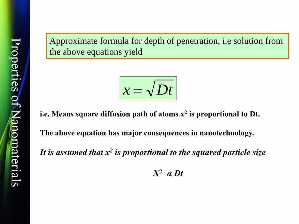
Approximate formula for depth of penetration, i.e solution from
the above equations yield
Dtx
i.e. Means square diffusion path of atoms x2 is proportional to Dt.
The above equation has major consequences in nanotechnology.
It is assumed that x2 is proportional to the squared particle size
X2 α Dt

Pro
perties o
f Nan
om
aterials
Conventional materials have grains sizes above 10 microns
It is well known that at elevated temperatures, homogenization
time requires of the order of many hours
When considering materials grain sizes with less than 10 nm
(1/1000 the of conventional grain size)
The time for homogenization reduced by a factor of (103)2 = 106
Hence homogenization occur almost instantaneously
Thermally activated process will happen nearly instantaneouly
It is difficult to produce non equilibrium systems at elevated
temperatures

Pro
perties o
f Nan
om
aterials

Pro
perties o
f Nan
om
aterials
In general, atomic transport in nanocrystalline materials differs
substantially from that in coarse-grained or single-crystalline
materials.
This is due to the fact that, in nanocrystalline solids, the crystallite
interfaces provide paths of high diffusivity, whereas in more coarse-
grained crystals, volume self-diffusion or substitutional atom
diffusion is substantial generally only at temperatures greater than
approximately half the melting temperature
Nanocrystalline materials

Pro
perties o
f Nan
om
aterials
In the general case of interface diffusion in polycrystalline
materials, two simultaneous diffusion processes have to be
taken into account, i.e., rapid diffusion in the crystallite
interfaces (diffusion coefficient Db) accompanied by diffusion
from the interfaces and specimen surface into the volume of
the crystallites (diffusion coefficient Dv).
These regimes are characterized by appropriate ratios of the
diffusion length in the crystallites (∝ √Dvt , diffusion time, t)
and the crystallite diameter, d, or the interface thickness, δ.
In practice however, at the low temperatures at which most
diffusion experiments on nanocrystalline materials are
performed.

Pro
perties o
f Nan
om
aterials
Nanoscale Heat Transfer

Pro
perties o
f Nan
om
aterials
Heat transfer at nanoscale is of importance for many nanotechnology
applications
There are typically two types of problems
One is the management of heat generated in nanoscale devices to
maintain the functionality and reliability of these devices.
The other is to utilize nanostructures to manipulate the heat flow and
energy conversion
Examples
Thermal management of nanodevices are the heating issues in integrated
circuits and in semiconductor lasers
The manipulation of heat flow and energy conversion include
nanostructures for thermoelectric energy Conversion,
thermophotovoltaic power generation

Pro
perties o
f Nan
om
aterials
Heat transfer at nanoscale may differ significantly from that in macro-
and microscales.
With device or structure characteristic length scales becoming
comparable to the Mean free path
and
Wavelength of heat carriers (electrons, photons, phonons, and
molecules),
Classical laws are no longer valid and new approaches must be taken to
predict heat transfer at nanoscale
Pro
perties o
f Nan
om
aterials
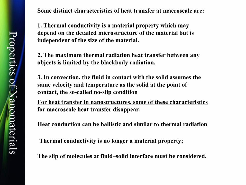
Some distinct characteristics of heat transfer at macroscale are:
1. Thermal conductivity is a material property which may
depend on the detailed microstructure of the material but is
independent of the size of the material.
2. The maximum thermal radiation heat transfer between any
objects is limited by the blackbody radiation.
3. In convection, the fluid in contact with the solid assumes the
same velocity and temperature as the solid at the point of
contact, the so-called no-slip condition
For heat transfer in nanostructures, some of these characteristics
for macroscale heat transfer disappear.
Heat conduction can be ballistic and similar to thermal radiation
Thermal conductivity is no longer a material property;
The slip of molecules at fluid–solid interface must be considered.

Pro
perties o
f Nan
om
aterials
From quantum mechanics, the energy carriers have both wave and
particle characteristics.
At macroscale, wave phenomena such as interference and tunneling
usually do not appear and we often treat the energy carriers as
particles.
At nanoscale, however, wave effects become important and even
dominant in some cases.
A key question is when one should start to consider the wave
characteristics.
There are a few important characteristic length and time scales
that determine the answer to this question
The mean free path,
the phase coherence length, the wavelength, and
the thermal (de Broglie) wavelength
Pro
perties o
f Nan
om
aterials
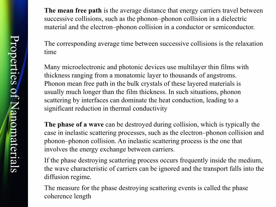
The mean free path is the average distance that energy carriers travel between
successive collisions, such as the phonon–phonon collision in a dielectric
material and the electron–phonon collision in a conductor or semiconductor.
The corresponding average time between successive collisions is the relaxation
time
The phase of a wave can be destroyed during collision, which is typically the
case in inelastic scattering processes, such as the electron–phonon collision and
phonon–phonon collision. An inelastic scattering process is the one that
involves the energy exchange between carriers.
If the phase destroying scattering process occurs frequently inside the medium,
the wave characteristic of carriers can be ignored and the transport falls into the
diffusion regime.
The measure for the phase destroying scattering events is called the phase
coherence length
Many microelectronic and photonic devices use multilayer thin films with
thickness ranging from a monatomic layer to thousands of angstroms.
Phonon mean free path in the bulk crystals of these layered materials is
usually much longer than the film thickness. In such situations, phonon
scattering by interfaces can dominate the heat conduction, leading to a
significant reduction in thermal conductivity

Pro
perties o
f Nan
om
aterials
Average wavelength of the energy carriers,
where v is the speed of carriers
Above Equations are also close to the but,
for accuracy, it is the thermal wavelength
Thermal de Broglie wavelength

Pro
perties o
f Nan
om
aterials
Convection is a process concerned with heat exchange between a solid surface
and a fluid. The energy transfer in convection is due to both molecular diffusion
and bulk motion of the fluid in the presence of a temperature difference. As in
conductive and radiative heat transfer, convection may also experience size
effects. For example, the mean free path of gas molecules becomes comparable
with the characteristic length of a nanostructure even at atmospheric pressures
One way to control thermal properties of liquids is the addition of small
particles to the liquid.
It has been observed that the addition of nanometer size particles dramatically
changes transport properties and enhances heat transfer performance of the
liquids
Photons can have a long mean free path as evidenced by the solar radiation
traveling to the earth and can also have a very short mean free path as the
rapid decay of electromagnetic waves inside a metal
Compared to phonons and electrons, however, the thermal wavelength of
the photons is actually very long and it is much easier to observe wave
effects (like Interference effects) for thermal radiation than in heat
conduction.
Because of the interference effects, radiation properties, such as emissivity
of thin films, can be thickness dependent
In pure metals electrons dominate the conduction, while in semiconductors
and insulators the dominant contribution comes from phonons.

Pro
perties o
f Nan
om
aterials
Catalysis by Gold Nanoparticles

Pro
perties o
f Nan
om
aterials
Although gold is the most inert of all metallic elements, it
has interesting properties as a heterogeneous catalyst
It has been widely believed until quite recently that
gold was too inert to be useful as a catalyst
Gold-based catalysts have been shown to have the best low temperature
activity for CO oxidation of all Catalysts.
It transforms carbon monoxide (CO) to carbon dioxide (CO2 )
Mechanism for the catalytic reaction 2CO + O2 -> 2CO2
This reaction is of great interest in terms of the purifying of indoor and in-vehicle air, and a
large number of studies have been conducted . In most of these studies the gold nano-
particles, generally of between 2 and 10 nm in size, have been supported on metal oxides of
various sorts.
However, very recently, a number of studies have shown how nano-
particles of gold lose their metallic nature as their size decreases, the
transition occurring at a size dependent on the chemical environment but,
as mentioned previously, certainly somewhere between 1 and 3 nm

Pro
perties o
f Nan
om
aterials
De-activation of gold catalysts
Many catalysts undergo some form of deactivation
during use and unfortunately, gold is no exception.
Sulphur and phosphorus are two of the few
elements with a strong affinity for metallic gold.
Therefore, it is expected that the activity of gold-
based catalysts will be readily poisoned in gas
streams containing these elements

Pro
perties o
f Nan
om
aterials
Crystal structure and morphology
In the bulk form gold has the face centred cubic (fcc)
structure which is closest-packed. Naturally-occurring
macro-crystals of native gold exhibit the highly symmetrical
cubic, octahedral crystal forms associated with this crystal
structure
Perfect clusters with fcc packing can be assembled
Au38, and Au116, Au140, Au225, Au314 and
Au459.

Pro
perties o
f Nan
om
aterials
MECHANISMS OF CATALYSIS
Active-perimeter models
The pioneering work by M. Haruta showed that activity in
gold catalysts could be associated with
hemispherical particles of Au with diameters of less than
about 5 nm, which are attached to oxide supports.
He, and several subsequent workers have concluded that it
was the perimeter of the hemisphere which was the active
site, at least for the CO oxidation reaction
In this model, the activity of the perimeter atoms of the gold cluster may be in a
special state controlled by electronic interactions with the oxide substrate. In
general, one of the reacting species, e.g. O2 would adsorb either at the perimeter
site itself or on the oxide support, and the other, e.g. CO, on the gold nanoparticle,
with the reaction between the two species occurring at the perimeter to produce
CO2. Either way, the nature of the support would control the reaction of O2 and
CO along the perimeter

Pro
perties o
f Nan
om
aterials
Active-particle (‘electronic’) model
The oxidation of CO on a heterogeneous gold catalyst evidently
requires that at least one molecule each of carbon monoxide and
oxygen come into contact with one another on the surface of the
gold nano-particle. Both gases have a negligible affinity for
bulk gold surfaces
However, very small nano-particles are obviously different and
direct evidence that both oxygen and carbon monoxide can
adsorb on neutral or negatively-charged gold nano-particles is
available.
Whetten and co-workers at Georgia Institute of Technology have
showed that O2 bonds readily with Aun with the oxygen attaching as a
superoxide (O2 -)
In this mechanism the role of the support is simply to modulate the
electronic structure of the cluster.

Pro
perties o
f Nan
om
aterials
The geometric models
If the surface of a material (or some site on the surface of the material)
has a particular ability to catalyse a chemical reaction, then it follows
that increasing the specific surface area (expressed as m2/g) of the
material will increase the activity of the catalyst.
In this scheme the chemical identity of the catalyst support is
completely unimportant; it exists solely to pin the catalytic particles
and prevent them from sintering together.
Much of the increase in catalytic activity of other metals and
materials may be explained entirely or substantially by the above
geometric argument.

Pro
perties o
f Nan
om
aterials
The manufacture of soft materials impacts nearly every sector
of modern life. Soft materials are primarily organic,
amorphous, and can be described as highly viscous fluids. They
form the basis of plastics used in consumer goods, automobiles,
aerospace, and other structural applications, but are also
important in higher efficiency energy solutions such as
membranes for fuel cells, water filtration and desalination, and
low energy displays. This class of materials is also at the heart
of the modern diet, as important proteins within foods,
preservative agents, and packaging materials. Soft materials are
also the primary component of cutting edge pharmaceutical
therapies, and are currently studied as potential solutions for
advanced tissue regeneration. As such, the field spans topics in
polymers, glasses, complex fluids, and many biomaterials.
Soft Materials and deposition

Pro
perties o
f Nan
om
aterials
This class of materials is defined by complexity, where structure is often
defined in terms of time scale. As a result, many manufacturing processes
occur far from equilibrium, and small variations in processing parameters
can drastically change material properties. The need to precisely and
accurately measure the response of soft materials to processing
parameters increases as new, more complex materials are desired to solve
issues confronting the modern world
Soft materials and complex fluids are ubiquitous not only in biology, but
also in industrial arenas as diverse as oil recovery, food technology,
cosmetics and personal care products, electronic devices, and
biotechnologies, such as microfluidics and targeted drug delivery.
Soft materials characteristically exhibit hierarchical structures organized on
multiple length-scales, which emerge from molecular and supra-molecular
self-assembly.

Pro
perties o
f Nan
om
aterials
A new technique for directly writing composites of
nanoparticles and polymers. Recent years have seen
significant advances in the properties achieved by both these
materials, and so researchers have begun to blend these
materials into nanocomposites that access the properties of
both materials. Forming these nanocomposites into
structures has been tricky since each nanocomposite would
require a particular set of solvents or a particular surface
coating.

Pro
perties o
f Nan
om
aterials
The technique builds on previous work using atomic force
microscopy (AFM) probes as pens to produce nanometer-
scale patterns. The polymer-nanocomposite blend is coated
onto the probe. When the probe is heated, it acts like a
miniature soldering iron to deposit the nanocomposite. "This
technique greatly simplifies nanocomposite deposition,"

Pro
perties o
f Nan
om
aterials
The technique also solves a common problem when depositing soft
materials like polymers and nanocomposites. The solvents and patterning
procedures for depositing soft materials can damage any soft material
already deposited. Consequently, it can be quite difficult to deposit many
different such materials. "Our ability to control nanometer-scale heat
sources allows local thermal processing of these nanocomposites,"
Although the nanoparticles were typically dispersed throughout the
nanocomposite, the researchers found that by adjusting the nanoparticle
chemistry they could force the nanoparticles into alignment. "With the
right chemistry, the forces in the polymer will guide the nanoparticles
into thin rows." Rows of nanoparticles less than 10 nm wide were
written, narrower than any other direct write technique. The string of
magnetic nanoparticles should be useful for studying magnetic
interactions on the smallest scales.

Pro
perties o
f Nan
om
aterials

Pro
perties o
f Nan
om
aterials
The presented study investigates the use of inkjet technology for the
deposition of cellulose nanocrystals onto flat substrates. Aqueous
suspensions of cellulose nanocrystals were printed onto glass
substrates using a commercial, piezoelectric, drop-on-demand inkjet
printer. Poor wetting of the glass substrates impeded the generation of
continuous films. However, printing of microdot arrays yielded regular
microscale arrays of nanocrystal deposits. Radial, outwards capillary
flow in the drying droplets led to ring formation but could be
suppressed by altering the surface chemistry of the glass substrate. Co-
deposition of a cellulose nanocrystal suspension and a chitosan
solution produced uniform, two-component deposits.

Pro
perties o
f Nan
om
aterials
Transport in quantum dots
Quantum dots are small electronic islands in which the motion
of the electrons is confined in all three spatial directions. Due to
the small (nanometer) length scales, the Coulomb interaction
between the electrons becomes important and gives rise to
intricate effects in experiments where electron transport through
the island is studied
The energy bands characteristic of macroscopic semiconducting
materials disappear and discrete levels appear. The quantum size
effects play an important role in the transport of electrons through
assemblies of quantum dots. The energy of the conduction levels
depend on the size of the dots.

Pro
perties o
f Nan
om
aterials
Another important feature of the quantum dot is the well-
resolved quantum levels. The electronic states of the quan-
tum dot can be modeled by “a particle in a box”, and the
energy levels in it is quantized, the spacing (∆E) of which
depends on the size of the box (quantum size effect). Again,
this size quantization effect becomes important in the
submicron dot typically below 1K.
A quantum dot has another characteristic, usually called the
charging energy, which is analogous to the ionization energy
of an atom. This is the energy required to add or remove a
single electron from the dot. Because of the analogies to real
atoms, quantum dots are sometimes referred to as artificial
atoms
Pro
perties o
f Nan
om
aterials
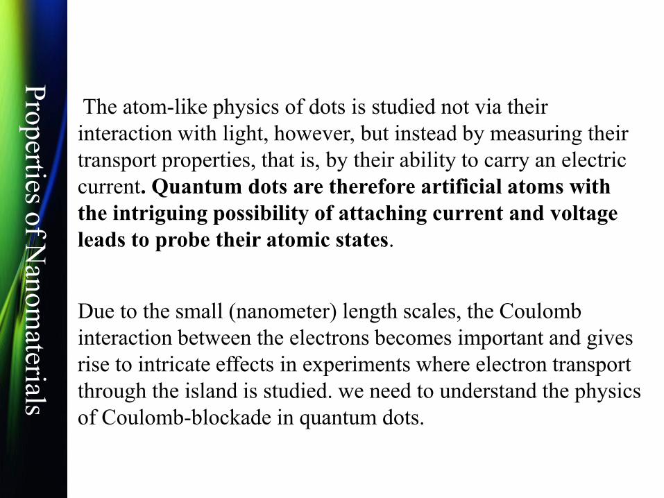
The atom-like physics of dots is studied not via their
interaction with light, however, but instead by measuring their
transport properties, that is, by their ability to carry an electric
current. Quantum dots are therefore artificial atoms with
the intriguing possibility of attaching current and voltage
leads to probe their atomic states.
Due to the small (nanometer) length scales, the Coulomb
interaction between the electrons becomes important and gives
rise to intricate effects in experiments where electron transport
through the island is studied. we need to understand the physics
of Coulomb-blockade in quantum dots.

Pro
perties o
f Nan
om
aterials
In a typical setup, one has source and drain leads with a
continuous density of states weakly coupled to central
conducting system with a discrete energy spectrum, usually
called “quantum dot,” the latter capacitively coupled to a gate
electrode
Weak coupling means that electrons can tunnel between leads and dot

Pro
perties o
f Nan
om
aterials
Single electron devices differ from conventional devices in the
sense that the electronic transport is governed by quantum
mechanics. Single electron devices consist of an „island‟, a
region containing localized electrons isolated by tunnel junctions
with barriers to electron tunneling
In order to let single electron tunnel through one atom to
another atom, the electron must overcome the Coulomb
blockade energy.

Pro
perties o
f Nan
om
aterials
Let us consider a nanoparticle sandwiched between
two metal electrodes . The nanoparticle is separated
from the electrodes by vacuum or insulation layer
(such as oxide or organic molecules) so that only
tunneling is allowed between them. So we can model
each of the nanoparticles-electrode junctions with a
resistor in parallel with a capacitor.

Pro
perties o
f Nan
om
aterials
The resistance is determined by the electron tunneling and the
capacitance depends on the size of the particle. We denote the
resistors and capacitors by R1, R2, C1and C2, and the applied
voltage between the electrodes by V. We will discuss how the
current, I, depends on V.
When we start to increase V from zero, no current can flow
between the electrodes because move an electron onto charging)
or off (discharging) from an initially neutral nanoparticle cost
energy by an amount of
where C is the capacitance of the nanoparticles. This suppression
of electron flow is called Coulomb blockade, first observed in the
60s by Giaever at GE in the tunneling junctions that contain
metal particles.

Pro
perties o
f Nan
om
aterials
Current start to flowthrough the nanoparticles only when the
applied voltage V is large enough to establish a voltage φ at the
nanoparticles such that
This voltage is called threshold voltage and denoted by Vth
. So in the I-V curve, we expect a flat zero-current regime
with a width of 2Vth. When the applied voltage reaches Vth, an
electron is added to (removed from) the nanoparticles.
Capacitor stores energy :
EC = C × V2/2
To charge a capacitor by 1e requires potential difference
V = e/C,
The charging energy EC
To observe SET effects the following condition must be fulfilled
EC>>kT
2C
e
2
C
e
C 2
VC E
2
2
2
C

Pro
perties o
f Nan
om
aterials
Further increasing the voltage, the current does not increase
proportionally because it requires us to add (or remove) two
electrons onto the nanoparticles, which cost a greater amount
of energy. Once the applied voltage is large enough to
overcome the Coulomb energy of two electrons, the current
starts to increase again. This leads to a stepwise increase in I-V
curve, called Coulomb staircase

Pro
perties o
f Nan
om
aterials
Ballistic conduction occurs when the length of
conductor is smaller than the electron mean-free path.
Another important aspect of ballistic transport is that
no energy is dissipated in the conduction
Ballistic conduction of carbon nanotubes was first
demonstrated by Frank and his co-workers in 1998.
The conductance of arc-produced multi-wall carbon
nanotubes is one unit of the conductance quantum Go,
and no heat dissipation is observed. Extremely high
stable current densities, have been attained.