ten-tec omni vi plus model 564 frequency adjustments
TRANSCRIPT

Ten-Tec Omni VI Plus Model 564 Frequency Adjustments
XTAL OSC. - L.O. MIXER BOARD (81595)
(The following was taken from the Omni VI Plus owner’s manual)
This module generates the main local oscillator signal which is applied to the transmit and receive mixers in the front end. Band switching information from the Logic board enters via connectors 82 and 83. One of the ten crystals is pin diode switched into oscillator stage Ql. Buffer stage Q2 drives one side of the LO mixer through a low pass filter and also drives the oscillator level detector D25, Q3. Transistor Q3 sets the bias point of the oscillator stage to stabilize the oscillator output level and to limit the drive in the crystals for better aging. Part of the crystal oscillator signal is fed through buffer transistor Q9 to the Logic board via connector 84. A PLL circuit on the Logic board compares this signal to a precision reference frequency and sends a d.c. correction voltage back to the oscillator via connector 84, through R26, R20 to varactor diode D26. This ensures that the crystal oscillator is always locked to a precision reference for improved frequency stability and accuracy. The synthesized 5.0 to 5.5 MHz signal at connector 85 is mixed with the crystal oscillator signal by active mixer Ul. The desired mixer product is filtered by one of five band pass filters and then amplified by transistors Q6, Q7 and Q8. The L.O. output is then taken off through ag MHztrap, T5 and C63, which helps eliminate undesired products from the mixer which could leak into the recever IF. ----------------------------------------------(End of Text)---------------------------------------------------------------------------
There are no alignment instructions for the circuit boards that control the receive and transmit frequencies. This document is an attempt to explain the alignment procedures for the 10 crystal oscillators that are located on the XTAL OSC – L.O. MIXER BOARD, the 10 MHz reference on the CPU board and the 5.0 to 5.5 MHz PLL board. Connect a frequency counter to pin 1 of U13. Adjust C31 for 10 MHZ. If there are erratic or frequency drift problems, there are probably failed capacitors on the CPU board. C36, a 33uF, 16 volt capacitor on the VDD pin of U13 is probably the culprit. A dried-out capacitor with high ESR can cause voltage spikes on the power lead of U13 and disrupt the DC Loop voltage on the Mixer/Oscillator board. Changing the capacitor can fix the problem and no further adjustments are needed. The CPU board is difficult to remove and in the process of removing it, there’s a chance that the board can get damaged. You can attach a capacitor across Pins 16 and 12 of U13. I used a 47uF, 16 volt (low ESR) polymer capacitor.

XTAL OSC. - L.O. MIXER BOARD MHz Frequency Adjustments
Remove the Top plate that covers the LO Mixer and 5.0 to 5.5 MHz boards. You can disconnect the cables marked ‘67’ and ‘V’ on the board marked Silk 82843 and cable marked ‘R’ on board 92870 (This won’t affect the adjustments).
If the 10 crystal oscillators need adjusting, you only need a volt meter. Connect a volt meter, or oscilloscope to the junction of R25 and R26.
Select the 160 meter band and adjust L12 for 3 volts on the meter. Adjust the other bands using the chart below.
L.O. MIXER BOARD (81595) MHz Frequency Adjustment Chart
Band Set Frequency Adjust Crystal Frequency
160 meters any frequency L12 for 3 v 16.300 MHz 80 meters any frequency L13 for 3 v 18.000 MHz 40 meters any frequency L18 for 3 v 21.350 MHz 30 meters any frequency L19 for 3 v 24.5017 MHz 20 meters any frequency Check 18.000 MHz 17 meters any frequency L14 for 3 v 32.500 MHz 15 meters any frequency L20 for 3 v 25.000 MHz 12 meters any frequency L21 for 3 v 28.500 MHz 10a meters 28.00 MHz L17 for 3 v 32.000 MHz 10b meters 28.55 MHz Check 32.500 MHz 10c meters 29.10 MHz L16 for 3 v 33.000 MHz 10d meters 29.55 MHz L15 for 3 v 33.500 MHz 80 and 20 meters use a common oscillator and the 20 meter adjustment is not needed 17 and 10b meters use a common oscillator and the 10 meter adjustment is not needed
NOTE; The five pass band filters adjustments are not needed.
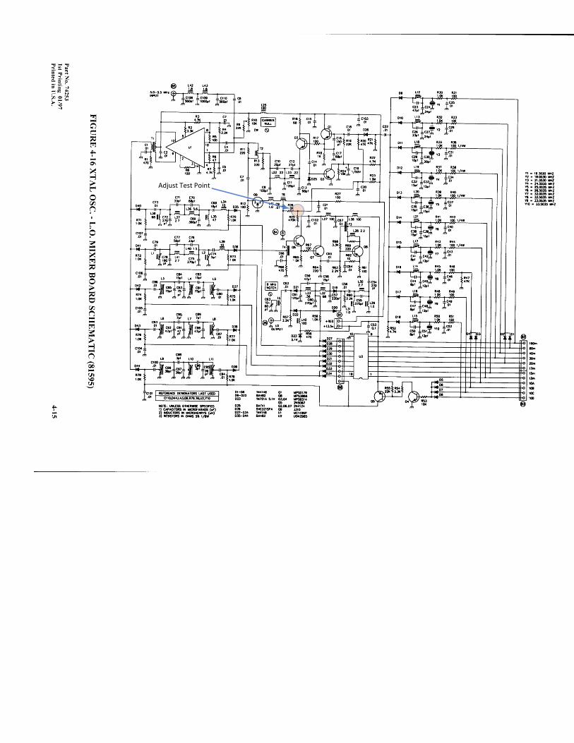
Adjust Test Point
4-8 5.0 - 5.55 MHz PLL BOARD (81599)
(The following was taken from the Omni VI Plus owner’s manual)
The phase noise characteristics of the OMNI VI depend entirely on the design of the 5.0 - 5.5 MHz synthesizer. The synthesizer is actually a two loop system that operates at 200 ti220 MHz and tunes in 400H2 steps. Its output is then divided by 40 to produce the desired 5.0 to 5.5 MHz output. This division by 40 not only reduces the output frequency but also reduces the phase noise and spurious levels by a factor of 32 dB. The synthesizet's l0 Hz tuning resolution is derived from a voltage controlled crystal oscillator (VXCO) Yl, Q2. Digital information from the microprocessor is clocked in serially to connector 87 and loads the shift register chip U3. The 8 bit output of U3 is applied to an R-2R resistor network, R23, which is used to provide digital-to-analo g conversion of the outputs of U3. U4A and U4B buffer the analog output from the resistor network and provide gain and offset adjustments (R27 and R3l) to align the frequency of VCXO. The VCXO output from Q2 is doubled by T2, D1 and D2, and then heavily filtered before it drives the diode mixer in the feedback path of the main loop. The mixer D3-D6 subtracts the VCXO frequency from the main loop's output which has been buffered by Q4. This difference signal becomes the feedback for the main loop. Q3 is a filtered amplifier stage which boosts the mixer output to a level sufficient to drive the prescaler chip U5. Since the loop works to keep this feedback signal constant in frequency, the small steps from the VCXO are imposed onto the main loop output. Reference and divide-by-N dividers in PLL chip U6 are programmed serially from the microprocessor through connector 87. The 10.0 MHz reference signal applied to connector 88 is divided internally in U6 by 1000 to generate a l0 kHz step size. Phase errors from the PLL's phase detector steer the charge pump circuit Q6- Q9. The VCO control voltage from the charge pump is low pass filtered and biases varicap diodes D9 and Dl0. The VCO output is applied to a two way splitter comprised of T5 and R49, and drives both the mixer buffer stage Q4 and the high speed divide-by-ten chip U7. The output of U7, a square wave of 20-22MHz, clocks a divide-by-four circuit in U8. The 5.0 to 5.5 MHz signal from U8 is then filtered to remove harmonics and exits to the LO mixer board. ----------------------------------------------(End of Text)---------------------------------------------------------------------------
5.0 - 5.55 MHz Frequency Adjustments. Set the receive Frequency to 14.0000 MHz, Lower Side-band. Connect a frequency counter to the TMP jack #85. Adjust L6 for 5.00 MHz. Adjust the receive frequency to 14.0024 MHz. the frequency counter should read 5.0024 MHz. If it does not R31 and R27 will need adjusting. Connect a volt meter to U4A pin 1. Starting at 14.0000MHz, slowly tune to 14.0024 MHz. The voltage should change approximately between 1.7 and 6.3 volts. Changing R31 clockwise increases the gain and R27 clockwise increases the offset. When the 5 MHZ changes in 10 Hz steps and the frequency change is greater than 10 Hz, the gain is too high. Back off on the gain (R31) and set the receive frequency to 14.0000. Readjust L6 to 5.000 MHz. Tune the receive frequency to 14.0024 and adjust R31 up or down to get 5.0024 MHz. When the frequency is close (within a few Hz) tuning back to 14.0000, you can then adjust R27 to 5.0000. Repeat the process until the frequency changes exactly in 10 Hz steps. There are other coils and trim potentiometers but because they don’t control the frequency, there’s no need to make further adjustments. There are BFO adjustments on the TX Audio Board that that will need tuning. The BFO adjustments are explained on page 4-23 and 4-24 on the Omni VI Plus Owner’s Manual.

Adjust Test Point