technology and manufacturing day · technology and manufacturing day 22ffl technology mark bohr...
TRANSCRIPT

Leading at the edgeTECHNOLOGY AND MANUFACTURING DAY
TECHNOLOGY AND MANUFACTURING DAY
22FFLtechnologyMARK BOHRIntel Senior Fellow, Technology and Manufacturing GroupDirector, Process Architecture and Integration

TECHNOLOGY AND MANUFACTURING DAY
Intel Technology and Manufacturing Day 2017 occurs during Intel’s “Quiet Period,” before Intel announces its 2017 firstquarter financial and operating results. Therefore, presenters will not be addressing first quarter information duringthis year’s program.
Statements in this presentation that refer to forecasts, future plans and expectations are forward-looking statementsthat involve a number of risks and uncertainties. Words such as “anticipates,” “expects,” “intends,” “goals,” “plans,”“believes,” “seeks,” “estimates,” “continues,” “may,” “will,” “would,” “should,” “could,” and variations of such words andsimilar expressions are intended to identify such forward-looking statements. Statements that refer to or are based onprojections, uncertain events or assumptions also identify forward-looking statements. Such statements are based onmanagement’s expectations as of March 28, 2017, and involve many risks and uncertainties that could cause actualresults to differ materially from those expressed or implied in these forward-looking statements. Important factors thatcould cause actual results to differ materially from the company’s expectations are set forth in Intel’s earnings releasedated January 26, 2017, which is included as an exhibit to Intel’s Form 8-K furnished to the SEC on such date.Additional information regarding these and other factors that could affect Intel’s results is included in Intel’s SEC filings,including the company’s most recent reports on Forms 10-K, 10-Q and 8-K reports may be obtained by visiting ourInvestor Relations website at www.intc.com or the SEC’s website at www.sec.gov.
Disclosures

TECHNOLOGY AND MANUFACTURING DAY
22FFL is the world’s first FinFET technology for low power IOT and mobile products
Advanced FinFET transistors based on proven 22 nm and 14 nm features
>100x leakage power reduction with new ultra-low leakage transistor option
Simplified interconnects and design rules based on 22 nm technology
New levels of design automation
Fully RF design enabled
Cost competitive with other industry 28/22 nm planar technologies
Intel’s new 22FFL technology
Source: Amalgamation of analyst data and Intel analysis, based upon current expectations and available information.
TECHNOLOGY AND MANUFACTURING DAY
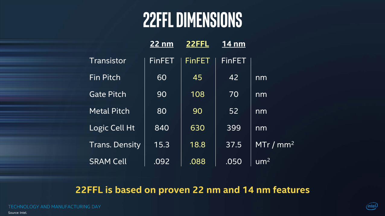
22FFL dimensions22 nm 22FFL 14 nm
Transistor FinFET FinFET FinFET
Fin Pitch 60 45 42 nm
Gate Pitch 90 108 70 nm
Metal Pitch 80 90 52 nm
Logic Cell Ht 840 630 399 nm
Trans. Density 15.3 18.8 37.5 MTr / mm2
SRAM Cell .092 .088 .050 um2
22FFL is based on proven 22 nm and 14 nm features
Source: Intel.

TECHNOLOGY AND MANUFACTURING DAY
22FFL devices
High performance transistors
Ultra low leakage transistors
Analog transistors
High voltage I/O transistors
High voltage power transistors
Good device matching
22FFL offers a wide range of devices for digital and analog/RF design
Low 1/F noise
Deep N-well isolation
Precision resistor
MIM capacitor
High resistance substrate
High-Q inductors
Source: Intel.

TECHNOLOGY AND MANUFACTURING DAY
FinFET Performance and leakage Advantage
FinFETs provide a significant performance and leakage advantage over any planar transistor
Intel 22 nm Tri-Gate announcement, April 2011
2.0
0.6
0.8
1.0
1.2
1.4
1.6
1.8
0.5 0.6 0.7 0.8 0.9 1.0 1.1Operating Voltage (V)
TransistorGate Delay(normalized)
22 nm Tri-Gate
32 nmPlanar
18% Faster
37% Faster
1E-05
0.0001
0.001
0.01
0.1
1
10
0.0 0.2 0.4 0.6 0.8 1.0
Planar
Tri-Gate
Reduced Leakage
Gate Voltage (V)
Channel Current
(normalized)
Source: Intel.
TECHNOLOGY AND MANUFACTURING DAY
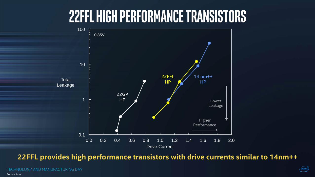
22FFl high performance transistors
22FFL provides high performance transistors with drive currents similar to 14nm++
0.1
1
10
100
0.0 0.2 0.4 0.6 0.8 1.0 1.2 1.4 1.6 1.8 2.0
Total Leakage
Drive Current
22FFLHP
22GPHP
14 nm++HP
0.85V
Lower Leakage
Higher Performance
Source: Intel.

TECHNOLOGY AND MANUFACTURING DAY
22FFL Low leakage transistors
22FFL provides the lowest leakage transistors for any mainstream technology
0.0001
0.001
0.01
0.1
1
10
100
0.0 0.2 0.4 0.6 0.8 1.0 1.2 1.4 1.6 1.8 2.0
Total Leakage
Drive Current
22FFLHP
22FFLLow Leakage
(LL)
22GPHP
14 nm++HP
>100x
0.85V
Lower Leakage
Higher Performance
Source: Intel.

TECHNOLOGY AND MANUFACTURING DAY
22FFL transistor Options
High performance and low leakage transistors co-exist on the same die
HP transistors for high performance
circuits
LL transistors for always-on always-connected circuits
0.0001
0.001
0.01
0.1
1
10
100
0.0 0.2 0.4 0.6 0.8 1.0 1.2 1.4 1.6 1.8 2.0
Total Leakage
Drive Current
22FFLHP
22FFLLow Leakage
(LL)
0.85V
Lower Leakage
Higher Performance
Source: Intel.

TECHNOLOGY AND MANUFACTURING DAY
Design Service
Soft IP
Advanced IPFoundation IP
Design Tools & Flows
Intel Custom
Foundry
Intel Custom Foundry’s robust Ecosystem
22FFL is fully supported by a robust design ecosystem
Other names and brands may be claimed as the property of others.

TECHNOLOGY AND MANUFACTURING DAY
22FFL is an exciting new technology that provides a compelling combination of performance, power, density and ease-of-design for low power IOT and mobile products
22FFL technology High transistor drive currents similar to Intel 14 nm
Low leakage transistors with >100x lower total leakage than 22GP
Die area scaling better than industry 28/22 nm technologies
Wide range of advanced analog/RF devices
Extensive use of single patterning for affordable ease-of-design
Mature die yield with use of proven 22/14 nm features
Cost competitive with other 28/22 nm planar technologies
Industry standard PDK0.5 available now, PDK1.0 in Q2 ’17*
Production readiness in Q4 2017*
* Intel estimate based on current expectations and available information.

Leading at the edgeTECHNOLOGY AND MANUFACTURING DAY