technical principles of electronics housings...technical principles of electronics housings |...
TRANSCRIPT

Technical principles of electronics housingsSolutions for DIN rail use
2 PhoEnIx ConTACT
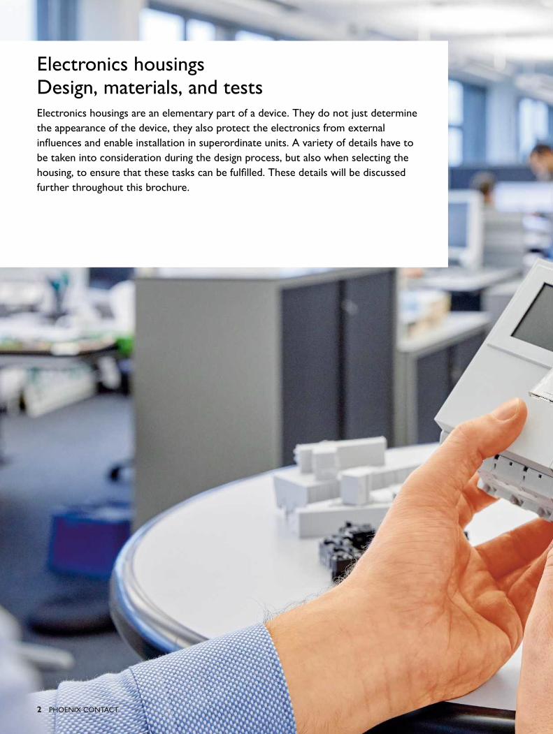
Electronics housingsDesign, materials, and testsElectronics housings are an elementary part of a device. They do not just determine
the appearance of the device, they also protect the electronics from external
infl uences and enable installation in superordinate units. A variety of details have to
be taken into consideration during the design process, but also when selecting the
housing, to ensure that these tasks can be fulfi lled. These details will be discussed
further throughout this brochure.
PhoEnIx ConTACT 3
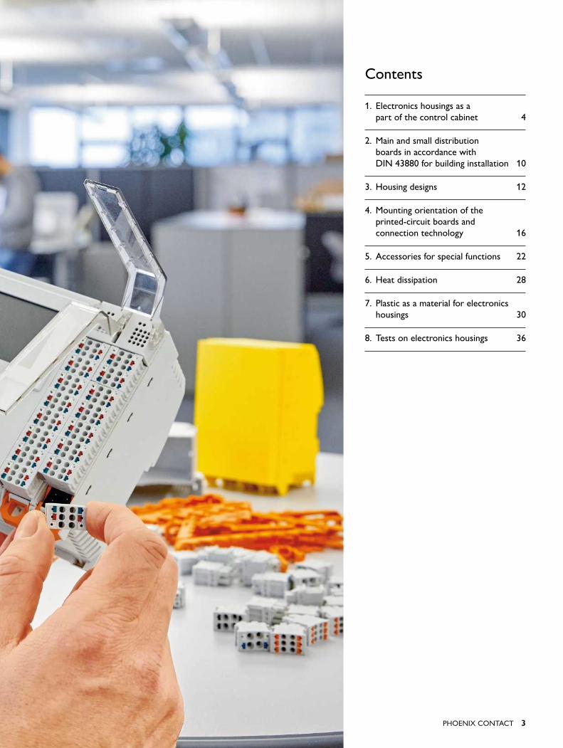
Contents
1. Electronics housings as a
part of the control cabinet 4
2. Main and small distribution
boards in accordance with
DIN 43880 for building installation 10
3. Housing designs 12
4. Mounting orientation of the
printed-circuit boards and
connection technology 16
5. Accessories for special functions 22
6. Heat dissipation 28
7. Plastic as a material for electronics
housings 30
8. Tests on electronics housings 36
1
4 PhoEnIx ConTACT
Technical principles of electronics housings | Electronics housings as a part of the control cabinet
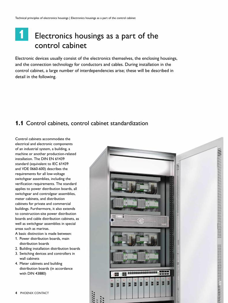
Electronics housings as a part of the control cabinet
Electronic devices usually consist of the electronics themselves, the enclosing housings,
and the connection technology for conductors and cables. During installation in the
control cabinet, a large number of interdependencies arise; these will be described in
detail in the following.
1.1 Control cabinets, control cabinet standardization
Control cabinets accommodate the
electrical and electronic components
of an industrial system, a building, a
machine or another production-related
installation. The DIN EN 61439
standard (equivalent to IEC 61439
and VDE 0660-600) describes the
requirements for all low-voltage
switchgear assemblies, including the
verifi cation requirements. The standard
applies to power distribution boards, all
switchgear and controlgear assemblies,
meter cabinets, and distribution
cabinets for private and commercial
buildings. Furthermore, it also extends
to construction-site power distribution
boards and cable distribution cabinets, as
well as switchgear assemblies in special
areas such as marinas.
A basic distinction is made between:
1. Power distribution boards, main
distribution boards
2. Building installation distribution boards
3. Switching devices and controllers in
wall cabinets
4. Meter cabinets and building
distribution boards (in accordance
with DIN 43880)
PhoEnIx ConTACT 5
Technical principles of electronics housings | Electronics housings as a part of the control cabinet
1.2 DIN rail mounting in the control cabinet
There are three main methods
of mounting the DIN rails for
accommodating devices and terminal
blocks, depending on the control cabinet
version and make (see Figs. 2-4).
In larger industrial control cabinets,
the DIN rails can be positioned
individually. This applies both to control
cabinets with a mounting plate and those
with a carrier frame. Holes are pre-drilled
to enable easier mounting. Terminal
housings and junction boxes are often
designed with screw bosses for mounting
DIN rails or small mounting plates. In
building installation distribution boards,
the DIN rails are screwed or riveted to
a frame with a clearance of 125 mm. The
riveted versions can only be moved with
a certain amount of eff ort.
How the DIN rails are mounted in the
control cabinet is of great importance for
the design of the electronics housings.
Depending on the control cabinet, the
DIN rails are either free-fl oating on a
carrier frame with clearance to the rear
panel or screwed directly onto the rear
panel or onto an inlaid mounting plate.
In cases where the devices are too heavy
for DIN rail mounting, or if there is not
a suitable DIN rail mounting option
on the device (see also page 7, Fig. 9),
devices are also mounted directly onto
a mounting plate without the use of a
DIN rail.
Fig. 2: Mounted onto the control cabinet rear panel
via raised screw boss
Fig. 3: Mounted on a carrier frame with clearance to
the rear panel
Fig. 4: Mounted directly on a mounting plate
Fig. 1: DIN EN 61439 structure
DIN EN 61439-1, Supplement 1: Guidance to specifying low-voltage switchgear and
controlgear assemblies
DIN EN 61439-1: General rules for low-voltage switchgear and controlgear assemblies
DIN EN 61439-6:
Busbar trunking systems
DIN EN 61439-5:
Cable distribution
cabinets
DIN EN 61439-3:
Building installation
distribution boards
DIN EN 61439-2:
Power switchgear and
controlgear assemblies
(PSC)
DIN EN 61439-4:
Assemblies for
construction sites
DIN IEC/TS 61439-7:
Assemblies for marinas,
camping sites, market
squares, and charging
stations
15°
>9
0
15°
>9
0
15°
>9
0
15°
>9
0
6 PhoEnIx ConTACT
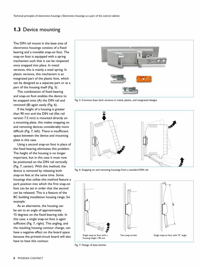
1.3 Device mounting
The DIN rail mount in the base area of
electronics housings consists of a fi xed
bearing and a movable snap-on foot. The
snap-on foot is equipped with a spring
mechanism such that it can be reopened
once snapped into place. In metal
versions, this is mainly a steel spring. In
plastic versions, this mechanism is an
integrated part of the plastic foot, which
can be designed as a separate part or as a
part of the housing itself (Fig. 5).
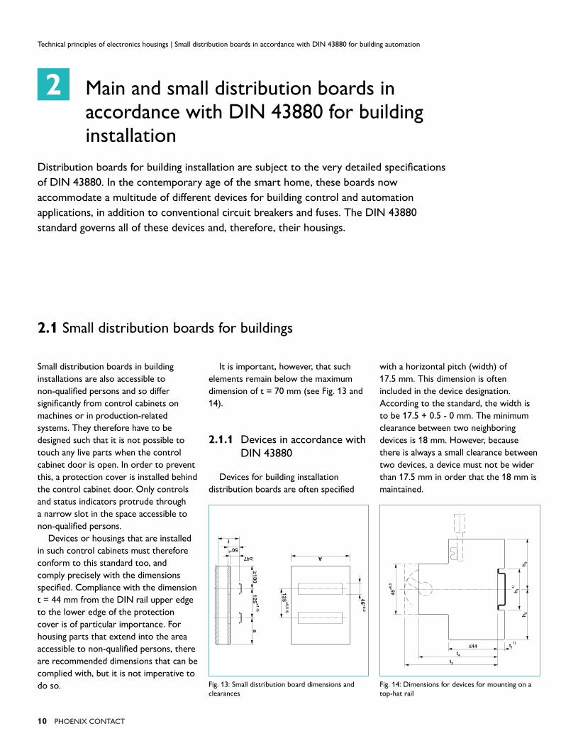
This combination of fi xed bearing
and snap-on foot enables the device to
be snapped onto (A) the DIN rail and
removed (B) again easily (Fig. 6).
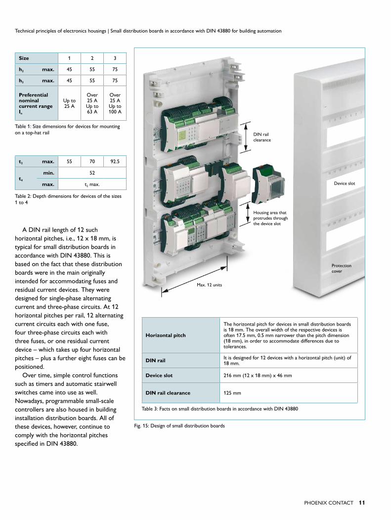
If the height of a housing is greater
than 90 mm and the DIN rail (fl at rail
version 7.5 mm) is mounted directly on
a mounting plate, this makes snapping on
and removing devices considerably more
diffi cult (Fig. 7, left). There is insuffi cient
space between the device and mounting
plate in this case.
Using a second snap-on foot in place of
the fi xed bearing eliminates this problem.
The height of the housing is no longer
important, but in this case it must now
be positioned on the DIN rail vertically
(Fig. 7, center). With this method, the
device is removed by releasing both
snap-on feet at the same time. Some
housings that utilize this method feature a
park position into which the fi rst snap-on
foot can be set in order that the second
can be released. This is a feature of the
BC building installation housing range, for
example.
As an alternative, the housing can
be set to an angle of approximately
15 degrees on the fi xed bearing side. In
this case, a single snap-on foot is again
suffi cient (Fig. 7, right). This angling, and
the resulting housing contour change, can
have a negative eff ect on the board space
because the printed-circuit board will also
have to have this contour.
Technical principles of electronics housings | Electronics housings as a part of the control cabinet
Single snap-on foot with a
housing height >90 mm
Two snap-on feet Single snap-on foot with 15° angle
Fig. 7: Design of base latches
Fig. 6: Snapping on and removing housings from a standard DIN rail
Fig. 5: Common base latch versions in metal, plastic, and integrated designs

PhoEnIx ConTACT 7
1.4 Standardized DIN rails in accordance with DIN EN 60715
The introduction of thermoplastics into
electromechanical engineering opened
up completely new base latch design
possibilities. Whereas previously, several
individual parts were required for the
construction of a snap-on foot, the new
material enabled the direct injection of
DIN rail feet, in particular on terminal
blocks. As a result, the simple top-hat rail
with a C profi le became the preferred
choice instead of the more complex G
profi le. Today, the 35 / 7.5 top-hat rail
described in DIN EN 60715 is the most
commonly used.
1.5 Mounting feet for heavy devices
Housings with integrated DIN rail feet
are used for devices that have an overall
weight of up to several hundred grams.
Signifi cantly heavier devices which are
also exposed to vibrations in certain
circumstances must be attached more
securely. DIN rail adapters, mainly of
metal, that are designed precisely for this
requirement are available for this type of
device.
Once the DIN rail adapter has been
attached to the device, both can then be
snapped onto the DIN rail. This solution
is often used for power supplies and
frequency converters.
These adapters are frequently also
used with sheet-metal housings, where
integrating snap-on feet into the design
is much more diffi cult than with plastic
housings.
Fig. 8: Standardized DIN rails in accordance with DIN EN 60715
Technical principles of electronics housings | Electronics housings as a part of the control cabinet
Top-hat rails
15 mm
35 mm
35 mm
105 mm
7.5 mm
15 mm
20 mm
5 mm
C rails
20 / 30 mm
40 / 50 mm
22.5 / 30 mm
18 / 22 mm
11 / 16 mm
10 / 15 mm
G rail
16.5 mm
6 mm
15 mm
32 mm
Fig. 9: Heavy-duty UTA DIN rail adapters in various versions

8 PhoEnIx ConTACT
1.6 Eff ect of the housings and connection technology on the control cabinet
design
The availability of space is a key criterion
in the selection of a control cabinet.
Housings, connection technology, and
the resulting conductor routing all have
diff ering space requirements. The design
of a housing therefore has a direct
infl uence on the control cabinet design.
With housings with front connection
technology, the cables are normally
only routed in one direction from the
housing into a cable duct. Such housings
are therefore ideally suited for mounting
directly on the control cabinet outer wall.
Because the cables enter the connection
block vertically, they can only be routed
in an arc into the cable duct. The selected
control cabinet must therefore be deep
enough to enable this type of conductor
routing.
Housings of the DIN 43880 design
have a similar limitation. In this case, the
protection cover in the standardized
control cabinet limits the wiring space. In
this installation situation, the conductor
outlet should preferably run parallel to
the control cabinet rear panel or at a 45°
angle to it. A conductor outlet angled at
90° to the control cabinet rear panel can
only be realized if low-profi le connection
terminal blocks are used (Fig. 10).
This also applies to plastic profi le
housings. However, in this case there are
not normally any limitations imposed due
to a standardized control cabinet type.
In control cabinet manufacturing, the
height of a device and the conductor
outlet direction are key criteria in the
design of a control cabinet. In order
to save costs and space, the control
cabinet must be as compact as possible,
but at the same it must be able to
accommodate any unplanned extensions.
The device with the greatest height
on a DIN rail defi nes the clearance
of the cable ducts, and therefore also
determines the total number of possible
DIN rails in a control cabinet. Where
there are only minor height diff erences
(Fig. 12), the typical basic setup is used:
cable duct – DIN rail – cable duct. If
there are just a few particularly tall
devices necessary, the usual setup is
adapted to best utilize the space available
(Fig. 12, bottom right).
In the case of front wiring with
conductor outlets on one side only,
a cable duct is only necessary on this
Technical principles of electronics housings | Electronics housings as a part of the control cabinet
Front wiring Conductor outlet with
conductors arced on both
sides
Conductor outlet with
conductors kept short on
both sides
Profi le housing conductor
outlet
DIN 43880 housing
conductor outlet
Fig. 10: Wiring

PhoEnIx ConTACT 9
side. Such devices can therefore be
installed on the upper area of the
control cabinet panel to save space
(Fig. 11). These front connections make
wiring the device easier, because the
electrician has a clear view of the contact
points. Front connection provides the
highest level of wiring convenience,
in particular when large numbers of
small conductor cross sections have to
be connected. In contrast to devices
with side connections, however, the
conductors unfortunately cover a large
part of the front of the device. Device
markings and indicators can therefore
only be positioned on the side of the
device. This limitation is accepted in
many applications, such as in remote I/O
systems.
Some housing systems enable very
short conductor routing if the conductor
outlet of the connection technology is
angled toward the cable duct (Fig. 10,
bottom left). In this case, it must be
noted that the conductors or plugs have
to be disconnected and reconnected
during service actions. Even if the device
or housing design enables shorter
conductors, conductors that are too
short will hamper any service actions.
Space for tall
devices to be
mounted directly
on the mounting
plate
Fig. 12: Classic control cabinet segmentation: cable duct – DIN rail – cable duct
Technical principles of electronics housings | Electronics housings as a part of the control cabinet
Fig. 11: Front connection technology with cable outlet on one side and conductor outlet on both sides in
the cable ducts
≥1
00
12
5±
1 4
)a
50⁺¹
≥47
t4
6⁺⁰⁵
12
5±
0,5
4)
A
t1
1)
45
±0
,5
h1
1)
h3
h2
≤44
t4
t2
2
10 PhoEnIx ConTACT
2.1 Small distribution boards for buildings
Small distribution boards in building
installations are also accessible to
non-qualifi ed persons and so diff er
signifi cantly from control cabinets on
machines or in production-related
systems. They therefore have to be
designed such that it is not possible to
touch any live parts when the control
cabinet door is open. In order to prevent
this, a protection cover is installed behind
the control cabinet door. Only controls
and status indicators protrude through
a narrow slot in the space accessible to
non-qualifi ed persons.
Devices or housings that are installed
in such control cabinets must therefore
conform to this standard too, and
comply precisely with the dimensions
specifi ed. Compliance with the dimension
t = 44 mm from the DIN rail upper edge
to the lower edge of the protection
cover is of particular importance. For
housing parts that extend into the area
accessible to non-qualifi ed persons, there
are recommended dimensions that can be
complied with, but it is not imperative to
do so.
It is important, however, that such
elements remain below the maximum
dimension of t = 70 mm (see Fig. 13 and
14).
2.1.1 Devices in accordance with
DIN 43880
Devices for building installation
distribution boards are often specifi ed
with a horizontal pitch (width) of
17.5 mm. This dimension is often
included in the device designation.
According to the standard, the width is
to be 17.5 + 0.5 - 0 mm. The minimum
clearance between two neighboring
devices is 18 mm. However, because
there is always a small clearance between
two devices, a device must not be wider
than 17.5 mm in order that the 18 mm is
maintained.
Main and small distribution boards in accordance with DIN 43880 for building installation
Distribution boards for building installation are subject to the very detailed specifi cations
of DIN 43880. In the contemporary age of the smart home, these boards now
accommodate a multitude of diff erent devices for building control and automation
applications, in addition to conventional circuit breakers and fuses. The DIN 43880
standard governs all of these devices and, therefore, their housings.
Technical principles of electronics housings | Small distribution boards in accordance with DIN 43880 for building automation
Fig. 13: Small distribution board dimensions and
clearances
Fig. 14: Dimensions for devices for mounting on a
top-hat rail
PhoEnIx ConTACT 11
A DIN rail length of 12 such
horizontal pitches, i.e., 12 x 18 mm, is
typical for small distribution boards in
accordance with DIN 43880. This is
based on the fact that these distribution
boards were in the main originally
intended for accommodating fuses and
residual current devices. They were
designed for single-phase alternating
current and three-phase circuits. At 12
horizontal pitches per rail, 12 alternating
current circuits each with one fuse,
four three-phase circuits each with
three fuses, or one residual current
device – which takes up four horizontal
pitches – plus a further eight fuses can be
positioned.
Over time, simple control functions
such as timers and automatic stairwell
switches came into use as well.
Nowadays, programmable small-scale
controllers are also housed in building
installation distribution boards. All of
these devices, however, continue to
comply with the horizontal pitches
specifi ed in DIN 43880.
Horizontal pitch
The horizontal pitch for devices in small distribution boards is 18 mm. The overall width of the respective devices is often 17.5 mm, 0.5 mm narrower than the pitch dimension (18 mm), in order to accommodate diff erences due to tolerances.
DIN railIt is designed for 12 devices with a horizontal pitch (unit) of 18 mm.
Device slot 216 mm (12 x 18 mm) x 46 mm
DIN rail clearance 125 mm
Technical principles of electronics housings | Small distribution boards in accordance with DIN 43880 for building automation
Size 1 2 3
h2 max. 45 55 75
h3 max. 45 55 75
Preferential nominal current range In
Up to 25 A
Over 25 AUp to 63 A
Over 25 AUp to 100 A
t2 max. 55 70 92.5
t4
min. 52
max. t2 max.
Table 1: Size dimensions for devices for mounting
on a top-hat rail
Table 2: Depth dimensions for devices of the sizes
1 to 4
Fig. 15: Design of small distribution boards
Table 3: Facts on small distribution boards in accordance with DIN 43880
DIN rail
clearance
Housing area that
protrudes through
the device slot
Max. 12 units
Device slot
Protection
cover

3
12 PhoEnIx ConTACT
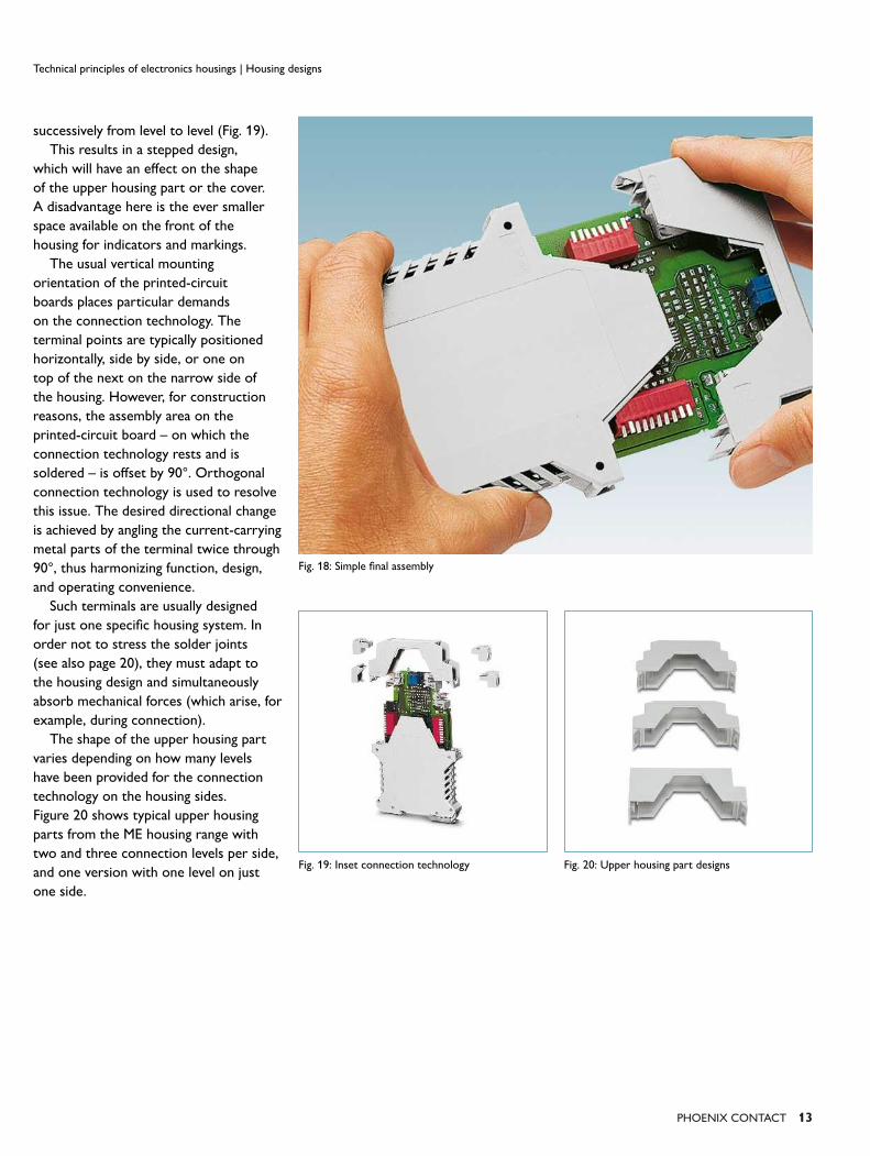
3.1 Modular electronics housings
Modular electronics housings feature a
cup design and consist of a single-piece
lower housing part – the cup – and
a housing cover. The connection
technology is normally positioned in the
cover or on the joint between the cover
and the cup (Fig. 18). If appropriate guides
are available, printed-circuit boards can
be inserted in all three spatial directions.
Thanks to the simple, two-piece design of
a modular electronics housing, rapid fi nal
assembly is possible (Fig. 18).
As already stated, the positioning of
the connection technology at the joint
between the cover and cup in modular
electronics housings is the best solution
from a mechanical perspective. If a lot of
terminal points are needed, the housing
size quickly limits the possible number of
terminal points per level.
If the connection technology is
distributed across several levels and good
terminal point accessibility is nevertheless
to be assured, it must be inset
Housing designs
Housings for electronic devices are split roughly into two groups: modular electronics
housings, which mainly consist of two parts, and half-shell housings, which consist of
several parts. There are also housings that are made of extruded profi les, but the term
PCB carrier is more suitable for these. With the fi rst two types, the design plays an
important role in addition to their function, whereas the focus for the latter type is mainly
on function.
Fig. 16: Basic design of modular electronics housings Fig. 17: Vertical PCB insertion in two spatial directions
Technical principles of electronics housings | Housing designs
PhoEnIx ConTACT 13
successively from level to level (Fig. 19).
This results in a stepped design,
which will have an eff ect on the shape
of the upper housing part or the cover.
A disadvantage here is the ever smaller
space available on the front of the
housing for indicators and markings.
The usual vertical mounting
orientation of the printed-circuit
boards places particular demands
on the connection technology. The
terminal points are typically positioned
horizontally, side by side, or one on
top of the next on the narrow side of
the housing. However, for construction
reasons, the assembly area on the
printed-circuit board – on which the
connection technology rests and is
soldered – is off set by 90°. Orthogonal
connection technology is used to resolve
this issue. The desired directional change
is achieved by angling the current-carrying
metal parts of the terminal twice through
90°, thus harmonizing function, design,
and operating convenience.
Such terminals are usually designed
for just one specifi c housing system. In
order not to stress the solder joints
(see also page 20), they must adapt to
the housing design and simultaneously
absorb mechanical forces (which arise, for
example, during connection).
The shape of the upper housing part
varies depending on how many levels
have been provided for the connection
technology on the housing sides.
Figure 20 shows typical upper housing
parts from the ME housing range with
two and three connection levels per side,
and one version with one level on just
one side.
Technical principles of electronics housings | Housing designs
Fig. 19: Inset connection technology Fig. 20: Upper housing part designs
Fig. 18: Simple fi nal assembly
14 PhoEnIx ConTACT
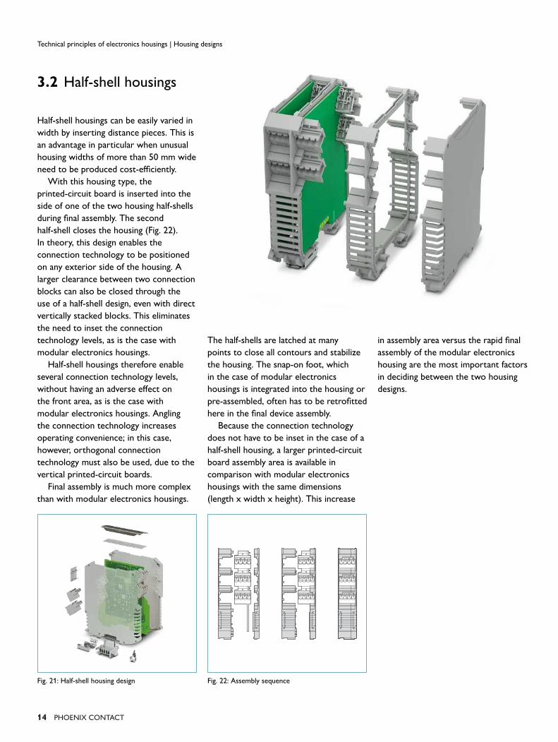
3.2 Half-shell housings
Half-shell housings can be easily varied in
width by inserting distance pieces. This is
an advantage in particular when unusual
housing widths of more than 50 mm wide
need to be produced cost-effi ciently.
With this housing type, the
printed-circuit board is inserted into the
side of one of the two housing half-shells
during fi nal assembly. The second
half-shell closes the housing (Fig. 22).
In theory, this design enables the
connection technology to be positioned
on any exterior side of the housing. A
larger clearance between two connection
blocks can also be closed through the
use of a half-shell design, even with direct
vertically stacked blocks. This eliminates
the need to inset the connection
technology levels, as is the case with
modular electronics housings.
Half-shell housings therefore enable
several connection technology levels,
without having an adverse eff ect on
the front area, as is the case with
modular electronics housings. Angling
the connection technology increases
operating convenience; in this case,
however, orthogonal connection
technology must also be used, due to the
vertical printed-circuit boards.
Final assembly is much more complex
than with modular electronics housings.
The half-shells are latched at many
points to close all contours and stabilize
the housing. The snap-on foot, which
in the case of modular electronics
housings is integrated into the housing or
pre-assembled, often has to be retrofi tted
here in the fi nal device assembly.
Because the connection technology
does not have to be inset in the case of a
half-shell housing, a larger printed-circuit
board assembly area is available in
comparison with modular electronics
housings with the same dimensions
(length x width x height). This increase
in assembly area versus the rapid fi nal
assembly of the modular electronics
housing are the most important factors
in deciding between the two housing
designs.
Fig. 21: Half-shell housing design Fig. 22: Assembly sequence
Technical principles of electronics housings | Housing designs
PhoEnIx ConTACT 15
3.3 Profi le housings
The term electronics housing is not
quite right for the profi le design. A more
suitable term here is PCB carrier. They
are manufactured from a continuous
extruded profi le, which is shortened
to a transportable length of 2 m after
production. The sections are then cut
to the desired length with millimeter
precision.
The profi les usually have several
grooves for accommodating
printed-circuit boards. A blocking
area is provided on the printed-circuit
board for this groove when positioning
the connection technology and the
electronics. With some designs, the
uppermost PCB receptacle can optionally
enable the connection technology to be
assembled on the edge (Fig. 24).
Side elements, which are available in
a variety of designs, are used to close
off the profi le ends. These are either
screwed onto the profi le or, in the case
of the rapid assembly versions, simply
snapped into place (Fig. 23). Because the
profi les do not have rear grooves due to
how they are processed, an additional cut
which serves as a rear groove for the side
elements is made when they are cut to
length.
The foot for mounting on the DIN rail
is integrated into the side elements.
As is the case with most housings, this
comprises a fi xed bearing and a fl exible
plastic part. The housing is completed
with a plastic cover, which is cut to the
respective length of the profi les.
Fig. 23: Screw-free side elements Fig. 24: Edge assembly on a profi le housing
Technical principles of electronics housings | Housing designs
Side element
Functional ground contact
Connection
technology
assembled on the
edge
Foot element
90°
0° 0°
90°
0°
45
° 90°
45
°
4
16 PhoEnIx ConTACT
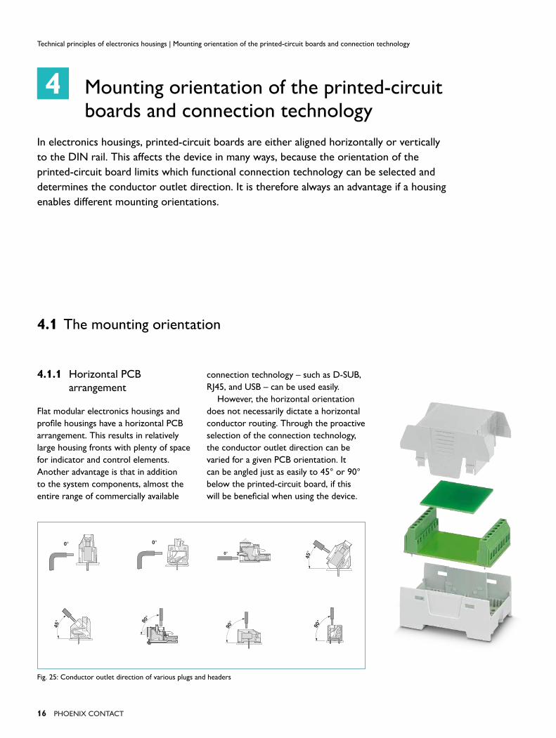
4.1 The mounting orientation
4.1.1 Horizontal PCB
arrangement
Flat modular electronics housings and
profi le housings have a horizontal PCB
arrangement. This results in relatively
large housing fronts with plenty of space
for indicator and control elements.
Another advantage is that in addition
to the system components, almost the
entire range of commercially available
connection technology – such as D-SUB,
RJ45, and USB – can be used easily.
However, the horizontal orientation
does not necessarily dictate a horizontal
conductor routing. Through the proactive
selection of the connection technology,
the conductor outlet direction can be
varied for a given PCB orientation. It
can be angled just as easily to 45° or 90°
below the printed-circuit board, if this
will be benefi cial when using the device.
Mounting orientation of the printed-circuit boards and connection technology
In electronics housings, printed-circuit boards are either aligned horizontally or vertically
to the DIN rail. This aff ects the device in many ways, because the orientation of the
printed-circuit board limits which functional connection technology can be selected and
determines the conductor outlet direction. It is therefore always an advantage if a housing
enables diff erent mounting orientations.
Technical principles of electronics housings | Mounting orientation of the printed-circuit boards and connection technology
Fig. 25: Conductor outlet direction of various plugs and headers

PCB 8
PCB 9
PCB 6
PCB 7
PCB 4
PCB 5
PCB 2
PCB 3
PCB 1
3,5
5
8,6 13
,65
18
,7 23
,75
26
,3
27
,61
30
,46
PhoEnIx ConTACT 17
Therefore, if a horizontal
printed-circuit board is selected, a
suffi cient level of freedom remains in
terms of the conductor outlet direction
(Fig. 25). With profi le housings,
the production method (extrusion)
almost exclusively dictates the
horizontal mounting orientation of the
printed-circuit boards.
A large number of housings also enable
the arrangement of printed-circuit boards
above one another in two or more levels.
Coding the levels is a good method of
making the fi nal assembly of such devices
easier. Thus, one printed-circuit board
fi ts exactly into one specifi c position
in the housing, and is mounted quickly
and securely. In the example shown in
Fig. 28, each PCB level is assigned at
least two square latch-in positions in the
housing side wall. Because these positions
are off set from level to level, there is
only one suitable PCB/latch-in point
combination per level.
4.1.2 Vertical PCB arrangement
The vertical PCB arrangement is used
in tall modular electronics housings and
half-shell housings. The printed-circuit
boards are guided into insertion grooves,
which are often provided for two spatial
directions. However, only a connection
technology that has been adapted for
this design can deliver the necessary
functionality.
In order to ensure that the operating
direction and conductor outlet are as
convenient as possible for the user – as
is the case with a horizontal orientation
– orthogonal connection terminal blocks
are needed (Fig. 26).
The actuator (in this case a connection
screw) and the solder connection are
in a line with the vertical printed-circuit
board. The solder/connector metals are
turned through 90° twice (orthogonal
connection technology) for the
conductor outlet. This enables the
terminal to be connected and operated
ergonomically. The integration of
third-party components is possible with
the vertical PCB orientation, but is not
as elegant, because such components are
usually only turned through 90° once.
Fig. 27: BC housing with 45° conductor outlet
Technical principles of electronics housings | Mounting orientation of the printed-circuit boards and connection technology
Fig. 26: Orthogonal MSTBO connection terminal
block
Fig. 28: Stacked PCBs in the BC housing

18 PhoEnIx ConTACT
4.2 Connection technology
There are two basic designs for the PCB
connection technology: fi xed connection
directly on the printed-circuit board, and
pluggable connection.
4.2.1 Fixed connection
The fi xed connection is of one piece and
connects the conductor directly to the
printed-circuit board. In comparison with
a pluggable solution, the fi xed connection
is more economical in terms of material
costs. In the event of service actions or
module replacements, the conductor
has to be detached then reconnected
later. If the conductors are not clearly
marked or labeled, this can lead to
incorrect connections, and therefore
to device damage. Terminals for a fi xed
connection are available in a huge range
of designs and colors. They come with
screw or spring technology, which ideally
can be used interchangeably in the same
layout. The wave soldering process is
typically used for one-piece terminals.
The high metal content is problematic
for processing using the refl ow soldering
process, because the one-piece design
includes screws or springs, terminal
sleeves, and solder pins. Firstly, the high
metal content at the soldering point
draws a great deal of heat, and secondly
it makes balancing on the printed-circuit
board more diffi cult.
The versions of this connection
technology are shown in Table 5 on
page 20.
4.2.2 Pluggable connection
Pluggable connections always consist
of at least two pieces. The conductors
are connected to a plug and are then
connected to the printed-circuit board
via a second component, the header.
Pluggable connections enable the rapid
replacement of devices. With these
connections, the danger of mismatching
connections when reconnecting is already
signifi cantly lower. Through the use of
coding and various colors, this danger can
be practically eliminated.
Thanks to the two-piece design, the
header to be soldered has only a low
metal content. It is therefore very light
and can be balanced easily for automatic
assembly. Pluggable solutions for both the
wave and refl ow soldering process are
available with the same layout (pinning).
The terminals for refl ow soldering
are made of a high-temperature plastic
in order that they can withstand the
temperatures in the soldering autoclave.
They are available in blister packs off the
roll for automatic assembly processes
(Fig. 30).
PropertyFixed connection
technologyPluggable connection
technology
Number of components 1 Min. 2
Contact resistance + -
Space required on the printed-circuit board + -
Flexibility in production - ++
Convenience in the event of service actions - ++
Refl ow-capable No Yes
Total costs due to number of parts + -
Control cabinet preassembly possible No Yes
Color versions available for function recognition Yes Yes
Coding Not necessary Yes
Technical principles of electronics housings | Mounting orientation of the printed-circuit boards and connection technology
Fig. 29: Comparison – fi xed vs. pluggable
Table 4: Comparison of fi xed and pluggable connections

PhoEnIx ConTACT 19
Fig. 31: Schematic illustration of the dependency between connection technology and production process
4.3 Dependence of the production process on the
connection technology
The choice of connection technology and
the subsequent production process are
closely interlinked.
The soldering process is defi ned in the
early stages of development. If an SMD
assembly with a refl ow soldering process
is decided upon, the use of single-piece,
fi xed connection technology is practically
ruled out, because there are very few
suitable products available on the market.
If the future device is to be made
available with fi xed connection
technology with both screw and spring
connection versions, one production line
is necessary for each version. The fi nal
product is therefore defi ned right at the
start of device production – during PCB
assembly. By the same token, a decision
to use fi xed connection technology is at
the same time a decision to use the wave
soldering production process.
An advantage of pluggable connection
technology is that there are identical
products available for both the refl ow
and wave soldering processes. Since the
conductor connection is located in the
plug and only added to the device at the
very end, the decision as to whether
the product will later have a Push-in,
screw or spring connection remains open
until the end of the production chain.
With pluggable connection technology,
therefore, a decision on the connection
method only needs to be made at
the end of the production chain. This
represents a signifi cant cost benefi t,
because all versions are produced on a
single line up until this point.
Fig. 30: Headers in blister packs off the roll
Technical principles of electronics housings | Mounting orientation of the printed-circuit boards and connection technology
Decision Eff ect
Nu
mb
er
of
pro
du
cti
on
lin
es
Development Production Delivery
Connection technology
Fixed
WaveProduction line Wave 1 Screw
Screw
Screw
Production line Wave 2 Spring
Spring
Spring
Production line Wave 3 Push-in
Push-in
Push-in
No technical solution
Wave
Refl ow
Refl ow
Pluggable
Soldering process Start Finished device
20 PhoEnIx ConTACT
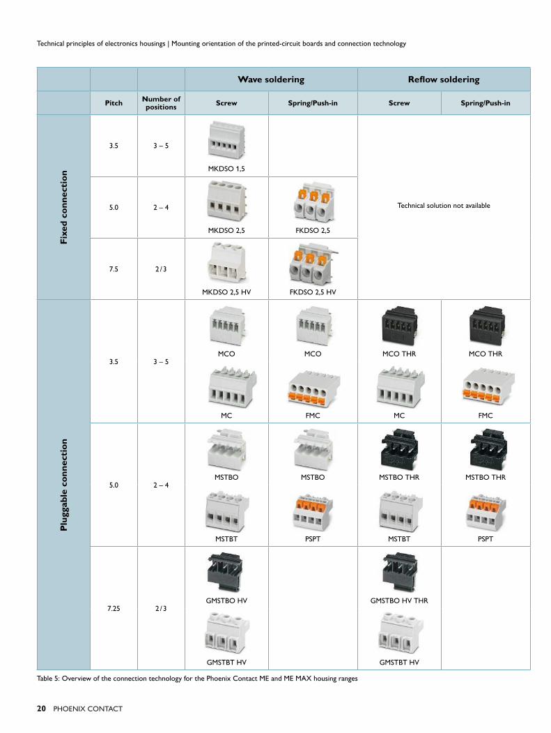
Wave soldering Refl ow soldering
PitchNumber of positions
Screw Spring/Push-in Screw Spring/Push-in
Fix
ed
co
nn
ecti
on
3.5 3 – 5
MKDSO 1,5
Technical solution not available5.0 2 – 4
MKDSO 2,5 FKDSO 2,5
7.5 2 / 3
MKDSO 2,5 HV FKDSO 2,5 HV
Plu
ggab
le c
on
necti
on
3.5 3 – 5MCO MCO MCO THR MCO THR
MC FMC MC FMC
5.0 2 – 4MSTBO MSTBO MSTBO THR MSTBO THR
MSTBT PSPT MSTBT PSPT
7.25 2 / 3GMSTBO HV GMSTBO HV THR
GMSTBT HV GMSTBT HV
Table 5: Overview of the connection technology for the Phoenix Contact ME and ME MAX housing ranges
Technical principles of electronics housings | Mounting orientation of the printed-circuit boards and connection technology
PhoEnIx ConTACT 21
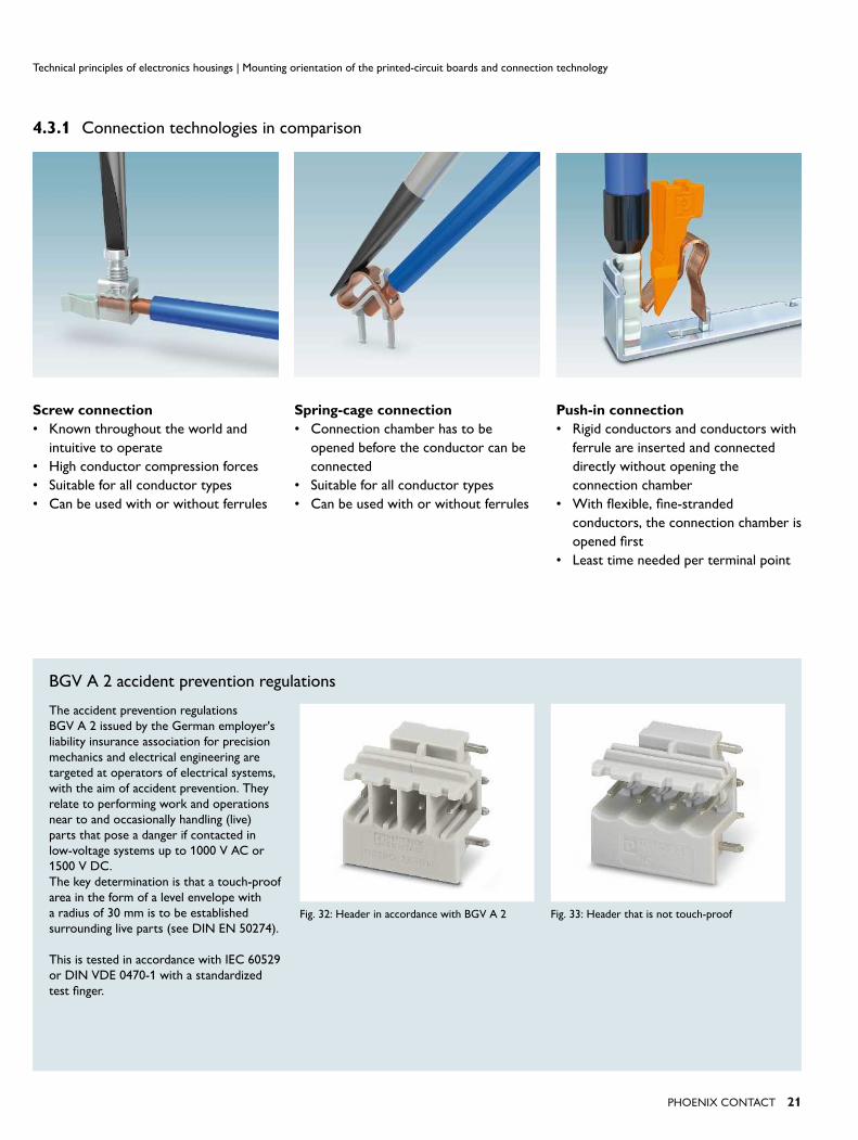
4.3.1 Connection technologies in comparison
BGV A 2 accident prevention regulations
The accident prevention regulations
BGV A 2 issued by the German employer's
liability insurance association for precision
mechanics and electrical engineering are
targeted at operators of electrical systems,
with the aim of accident prevention. They
relate to performing work and operations
near to and occasionally handling (live)
parts that pose a danger if contacted in
low-voltage systems up to 1000 V AC or
1500 V DC.
The key determination is that a touch-proof
area in the form of a level envelope with
a radius of 30 mm is to be established
surrounding live parts (see DIN EN 50274).
This is tested in accordance with IEC 60529
or DIN VDE 0470-1 with a standardized
test fi nger.
Fig. 32: Header in accordance with BGV A 2 Fig. 33: Header that is not touch-proof
Technical principles of electronics housings | Mounting orientation of the printed-circuit boards and connection technology
Screw connection
• Known throughout the world and
intuitive to operate
• High conductor compression forces
• Suitable for all conductor types
• Can be used with or without ferrules
Spring-cage connection
• Connection chamber has to be
opened before the conductor can be
connected
• Suitable for all conductor types
• Can be used with or without ferrules
Push-in connection
• Rigid conductors and conductors with
ferrule are inserted and connected
directly without opening the
connection chamber
• With fl exible, fi ne-stranded
conductors, the connection chamber is
opened fi rst
• Least time needed per terminal point
5
22 PhoEnIx ConTACT
Accessories for special functions
If adapted functional accessories are added to an electronics housing, the housing becomes
a housing system. Among others, these functional accessories include the previously
discussed connection technology, status indicator elements, and device-to-device
connectors (buses). They also include potential and shield connection elements.
5.1 LED status indicators
The implications of the printed-circuit
board mounting orientation are the same
for indicator and control elements as
they are for the connection technology.
With horizontal printed-circuit boards,
it is also possible to install light guides
with a relatively simple construction.
With vertical printed-circuit boards, the
light has to be redirected similarly to the
conductor path in orthogonal connection
technology. In contrast to the connection
technology, however, the light-emitting
surface is not the housing side panel, but
the housing front. With light guides, a
single 90° turn is therefore suffi cient.
Light guides are generally positioned
such that they pass through the housing
panel and terminate fl ush with the front
surface. If light guides have a rounded
light-emitting surface, this should
protrude from the front by the radius
of the rounding. Firstly, this avoids
dirt-collecting edges. Secondly, the angle
from which the indicated status can be
read off conveniently is increased.
Depending on the design, LEDs can
also be routed directly through the
housing front. Dirt-collecting edges are
also to be avoided here. Added to this
is the danger of ESD pulses that can
penetrate through the LED opening
into the housing interior. A partially
transparent fi lm label can be used as a
countermeasure to this.
Light guides are available in a huge
range of versions and designs. They must
ensure the low-loss transmission of light
and be highly homogeneous in design.
If this is not the case, two light guides
routed side by side may produce diff erent
lighting impressions. This can lead to
confusion when the user is determining
the device status.
Technical principles of electronics housings | Accessories for special functions
Fig. 34: Housing front with LED indicators
PhoEnIx ConTACT 23
5.1.1 Light guides with a high
packing density
Especially with housings with front
connection technology and a high
connection density, there is little space
available for status indicators (Fig. 35).
Light guides that enable a high packing
density are ideal for such cases. This
high packing density enables a light guide
block pitch of 2.54 mm and a diameter of
2 mm per light guide. These are normally
designed for CHIPLEDs of the type
0603 or smaller (Fig. 36). An aperture
integrated into the light guides prevents
the light being transmitted from one
light guide to the next, thus enabling the
display of diff erent colors in one block.
Press-in pins ensure secure positioning on
the printed-circuit board.
The light guide blocks can be adapted
to the application. Variations can be
created through diff erent numbers of
rows and columns, as well as partial
assembly and combinations. When using
light guide blocks, either the light guides
or the housing should have beveled edges
as insertion aids to simplify fi nal assembly.
Light guides are often made of
transparent polycarbonate. A material
of fl ammability rating of UL V0 (see also
page 34) is ideal, as this is frequently
required for electronics housings. With
an optimized lighting design in terms
of material, shape, and diameter, a
high-quality visualization system can then
be achieved.
5.1.2 Flexible light guides
When positioning light guides,
mechanical or electronic limits are
encountered in some applications. The
typical designs require proximity to the
indicator area, which is not always easy to
achieve if the electronics packing density
is high or if the housing geometries are
complicated. Flexible light guides (Fig. 37)
enable LEDs to be positioned practically
anywhere on the printed-circuit board.
The light is guided via two end caps
and a fl exible part, including in loops if
necessary. The light guides can be cut to
the optimum length via a careful incision
using a very sharp knife, and are therefore
ideal for these applications. For housings
with a high IP protection class, the light
exit cap can be affi xed with adhesive to
the front of the housing to form a water
and dust-proof bond, thus enabling an
easy-to-realize status indicator.
Technical principles of electronics housings | Accessories for special functions
Fig. 35: Light guides in the ME-IO housing for a
compact indicator area
Fig. 36: 5x4-row light guide block
Fig. 37: Flexible light guide
24 PhoEnIx ConTACT
Technical principles of electronics housings | Accessories for special functions
5.2 Bus systems
5.2.1 DIN rail buses and device
buses
Electronic control and regulation systems
are constructed by adding various
function modules, with the advantage
that individual components can be easily
added or removed. It is therefore simple
to convert or extend a system. This
requires that the function modules are
connected together via a bus system.
Two types of bus system have become
established: the DIN rail bus, which runs
below the housing in the DIN rail, and
the device bus, which is located inside the
housing.
The DIN rail bus can be mounted
independently of the housings and
enables individual housings to be
removed from an assembly (Fig. 38). The
bus communication is not automatically
interrupted when one bus module is
removed, meaning that the rest of the
system remains in operation.
With a device bus, which runs inside
a housing, it is not possible to remove
individual modules from the assembly
easily, because the neighboring modules
must fi rst be moved to one side (Fig. 39).
This interrupts the bus connection.
Only then can the selected module
be removed from the rail. Interrupting
communication is not permitted in a huge
number of applications, meaning that the
use of device buses is ruled out.
With device bus systems, the
connection between the bus and
device electronics (printed-circuit
board) is established during module
production. The printed-circuit board is
plugged vertically into the bus contact,
meaning that the contact between the
printed-circuit board and bus contact can
be simple in design.
The DIN rail bus system is completely
diff erent. In this case, due to the housing
construction, a module is not placed
vertically onto the DIN rail, but is pivoted
into place on the rail via the fi xed bearing
and snap-on foot (Fig. 40). The contacts
thus move along a circular path, which
must be refl ected in the geometry of the
contact pads on the printed-circuit board.
An ideal design would ensure that once
a contact has been made, it does not
break off due to the movement and that
the movement does not lead to a short
circuit or a violation of the minimum
clearance and creepage distances.
A good solution is to equip the outer
edge of the printed-circuit board in the
area of the bus contacts with a beveled
edge. This acts as an aid when opening
Fig. 41: Cross section of a housing with device bus
Fig. 40: Pivoting a device onto the DIN rail bus
Fig. 39: Basic design of a device bus system
Fig. 38: Basic design of a DIN rail bus

PhoEnIx ConTACT 25
Technical principles of electronics housings | Accessories for special functions
the bus contacts and provides mechanical
relief during the pivoting action.
Because the DIN rail bus follows a
specifi ed pitch, and because a vertical
outlet to a device or a device board
is not always necessary, appropriate
bridging adapters are available for this bus
type (Fig. 42).
DIN rail buses are available in 5- and
8-position versions. The buses are rated
for 6 ... 8 A at a voltage of up to 100 V.
The DIN rail buses feature exceptionally
good signal transmission characteristics,
even at high speeds. They are therefore
ideal for creating a local communication
bus.
5.2.2 Power buses
Device and DIN rail bus systems are
suitable for signal transmission even at
high frequencies, and for low-power
transmission. A current carrying capacity
of 5 ... 10 A is typical for such bus
systems. If higher powers are to be
distributed, additional rail distributors
have to be used, such as the power bus
system for the ME MAX housing range
shown in Fig. 43. Up to 30 devices can be
supplied via busbars that have a current
capacity of 40 A and special connection
elements. Because these busbars can be
installed in parallel to the DIN rail bus,
the contacts are designed such that the
devices can also be snapped into place
and pivoted.
5.2.3 Parallel and serial contacts
As with the device bus, the DIN rail bus
can be fi tted with parallel and with serial
contacts (Fig. 44). Parallel means that the
feed-in, branching, and forwarding share
the same potential.
Serial contacts are discontinuous
contacts. The connection between
feed-in and forwarding is established via
the device printed-circuit board. The
diff erent contact types can be combined
in any way and any number on one block.
However, due to the mechanical load, the
position and number of serial contacts
may be restricted.
Fig. 43: Power bus Fig. 44: Parallel and serial contacts
Fig. 42: Bus adapter for bridging

26 PhoEnIx ConTACT
Technical principles of electronics housings | Accessories for special functions
5.2.4 High-position buses
Wherever buses with a high number of
positions are required, DIN rail buses
quickly reach their physical limits. With
high numbers of positions, the contacts
are so delicate and the mechanical
pivoting forces are so high, that
deformations are to be expected.
It is easier to plug the housing onto
the bus perpendicularly. In this case,
pin and socket strips can be used on a
printed-circuit board as the basis for the
bus confi guration (Fig. 45/46). The use of
a printed-circuit board also enables the
integration of simple SMD components
into the bus, such as stabilization
capacitors for improving the EMC
properties.
A disadvantage is that such a system
often cannot work with the classic
snap-on foot/fi xed bearing principle;
instead, a second base latch is necessary,
which enables vertical plugging and
unplugging, and therefore ensures that
the sensitive contacts on the male side of
the bus are not damaged.
Because users will intuitively attempt
to pivot a module into place as is usual,
this deviation from the standard must be
clearly documented.
Buses that provide even more space
for electronics are those that are
designed for the large NS 105/20 DIN rail
(Fig. 47/48). Here, the power supply,
coding, confi guration elements, and
electronic repeaters can be integrated in
addition to the signal lines.
5.3 Function accessories
Housings, connection technology,
indicators, and bus systems form the
basic framework for a housing system.
Additional accessories enable these
to be used in a much larger range of
applications and for individual tasks, such
as the electrical connection of a device to
a grounded control cabinet.
If, for example, protective grounding
(protective earth, PE) is necessary, the
connection must be established to a
fi xed, non-pluggable connection terminal
block. If the connection technology
has been designed to be fully pluggable,
the PE contact must be designed to be
leading during plugging and lagging during
unplugging. Furthermore, a PE contact is
subject to special normative requirements
(e.g., cross sections, impulse durability).
If just one equipotential bonding line
for arresting static discharge is to be
established, or if functional grounding
(GND) is necessary, for example, as
a common reference point for a data
interface, then a functional ground
contact directly in the base area of the
housing with a connection to the DIN rail
is normally suffi cient (Fig. 49/50).
Such contacts, however, never satisfy
the electrical requirements that are
placed on PE contacts.
If the cable shielding of a signal line
is to be connected to the electronics,
shield connection clamps are used
(Fig. 51). Here, one terminal point of the
connection technology is occupied with
the terminal lug of the shield connection
clamp, and the exposed cable shielding is
inserted into the clamp and secured with
a screw, as is the case with a strain relief
system.
Note: When using shield connection
clamps and functional ground contacts at
the same time, it must be ensured that
this confi guration does not give rise to a
grounding loop. This would be the case
if the cable shielding were connected at
a second point in the control cabinet to
Fig. 45: Cross section of a DIN rail bus with
printed-circuit boards attached
Fig. 46: PCB-based high-position bus
Fig. 47: High-position bus in the NS 105/20 rail
Fig. 48: Individual parts of high-position bus

PhoEnIx ConTACT 27
Technical principles of electronics housings | Accessories for special functions
the cabinet itself or to the DIN rail. This
would close the DIN rail – functional
ground contact – printed-circuit board –
shield connection clamp – shielding –
DIN rail circuit, enabling interference
voltages to be induced easily in this
conductor loop, for example, during
switching operations.
Housings with a quick locking
system can also be opened easily during
operation. The use of pull-out stops
has proven to be eff ective in ensuring
that the printed-circuit board cannot be
inadvertently pulled completely out of
the housing. The printed-circuit board
can only be pulled completely out of the
housing once the pull-out stop has been
released.
Housings with a quick locking system
are also frequently used if settings
have to be made, for example, via
potentiometer or DIP switch on the
device printed-circuit board during
commissioning or in the event of service
actions. The PCB pull-out stop also
prevents the printed-circuit board from
being pulled completely out in this case.
Fig. 49: FE contacts for ME housings
Fig. 51: Shield connection clamp on an ME housing
Fig. 52: PCB pull-out stop
Fig. 50: FE contacts for UM profi les

6
28 PhoEnIx ConTACT
6.1 Heat transfer
A basic distinction is made between the
three types of heat transfer involved in
dissipating the heat from housings to the
surroundings:
6.1.1 Heat radiation
Bodies emit heat to their surroundings
via radiation. Because plastic, as the
typical material for electronics housings,
tends to insulate rather than conduct
heat, this eff ect is hardly noticeable.
Furthermore, devices for DIN rail
mounting are often arranged very close
to each other. This signifi cantly restricts
heat from being dissipated via the side
walls. It is also possible that neighboring
devices add additional heat. Better heat
dissipation is achieved by positioning
spacers between the devices. However,
they increase the space requirements and
must be taken into consideration early on
during control cabinet planning.
6.1.2 Convection
If housings are equipped with ventilation
slots on their narrow sides, a circulation
of air develops if they are installed
vertically: warm air rises and escapes via
the upper ventilation slots. Colder air is
drawn in through the lower ventilation
slots, which is then heated by the hot
components and, in turn, escapes through
the upper slots. The resulting natural
convection system only comes to a
standstill once the surroundings and
the device reach the same temperature
level. Normally, this point is never
reached, because the control cabinet
surrounding the device absorbs heat itself
and transfers this to the surroundings.
In order to prevent the ingress of larger,
solid foreign bodies, the maximum width
of the ventilation slots in electronics
housings is 2.5 mm, in accordance
with the protection class IP 3x of
DIN EN 60529.
Heat dissipation
An elementary challenge surrounding the operation of electronics housings is heat
dissipation, because the electrical and consequently the mechanical components inside
the housings heat up. In most cases, the critical temperatures for individual components
are not exceeded. If, however, components do reach their performance limits, there
must be suffi cient heat transfer to reduce the temperature, otherwise the device may
become damaged.
Technical principles of electronics housings | Heat dissipation

PhoEnIx ConTACT 29
6.1.3 Heat conduction
In this case, the heat transfer occurs
within a substance via its molecular
movements. With electronic devices,
it is often the connected copper wires
that dissipate a great deal of heat from
the inside of the housing to the outside.
This, of course, only happens if the live
copper wires are colder than the device
itself. Performing temperature tests
on connected cables with the nominal
cross section and under normal load and
typical installation conditions is therefore
recommended. This test setup should
also include neighboring devices or cable
ducts that impede heat transfer. Thermal
imaging cameras provide an overview
of the temperature conditions and heat
sources – known as hot spots – in a
housing.
6.2 Thermal simulation of electronic devices
The technical data of electronics
housings normally lists specifi cations
on the temperature behavior. Usually
this is the power dissipation, i.e., how
much power a housing can dissipate in
the selected design. Issues such as the
size of the housing, the material, the
mounting position, and the presence
of ventilation slots play a role here.
Thermal simulation has proven to be
a useful method of checking whether
the electronics to be introduced do not
cause these limits to be exceeded. This
method analyses the PCB layout to create
a thermal map that captures both the
active, heat-generating components and
the passive heat-sensitive components.
Software then simulates the development
of heat within the housing, the eff ect
on neighboring components, the heat
conduction, and heat radiation out of
the housing into the surroundings. If
ventilation slots are present and if the
mounting position enables convection,
this is also taken into consideration. With
this information, it quickly becomes clear
to what extent a housing is suitable for
the desired application. Furthermore,
the positioning of components can be
optimized with this analysis. Does, for
example, a particularly tall component
impede convection and need to be
moved?
The simulation itself is performed in
several steps. In the fi rst step, a type of
rough-calculation simulation determines
whether a device will even approach
the thermal limit range. If it will, a more
precise analysis of the thermal behavior
will be simulated in detail. Naturally, in
borderline cases, verifying the result in a
trial is to be recommended.
Technical principles of electronics housings | Heat dissipation
Fig. 53: Heat distribution without heatsink
Fig. 54: Unfavorable component positioning
Fig. 55: Heat distribution with heatsink
Fig. 56: More favorable component positioning
7
30 PhoEnIx ConTACT
7.1 Technical plastics
Plastics get their strength from this
macromolecular structure. They diff er
from each other due to:
• The type and arrangement of the
atoms involved in their structure
• The form of the macromolecules
• The size of the macromolecules
• The arrangement of the
macromolecules.
DIN 7728 specifi es the abbreviations
for the individual plastics.
Thermoplastics are often used for
electromechanical elements. These
plastics, which are tough and hard at
normal temperatures, can be repeatedly
heated to a plastically deformable state,
although they will be degraded somewhat.
Thermoplastics can be melted, welded,
swollen, and dissolved. They are
characterized by a low density, a relatively
high chemical resistance to inorganic
media, a high electrical insulating ability,
and their versatile mechanical behavior.
Disadvantages from an electromechanical
engineering perspective are the limited
temperature stability and the swelling
behavior.
More than 90% of the electronics
housings on the market today are made
of plastic due to the properties listed.
The advantage lies in the easy formability,
especially in mass production, in
conjunction with the very good insulation
properties and low weight.
However, not all thermoplastics have
exactly the same properties. There are
diff erences in the dimensional stability
and the application in certain temper-
ature ranges. The addition of fi berglass
increases the hardness and rigidity in
comparison with the base material.
7.1.1 Commonly used
thermoplastics
• Polyamide PA retains its electrical,
mechanical,and chemical properties,
which are very well suited to
electronics housings, even at high
operating temperatures. Through
heat stabilization, short-term peak
temperatures of up to approximately
200°C are permitted. The absorption
of water makes the plastic fl exible and
resistant to breakage.
• Polyamides (PA-GF) are polyamides
reinforced with fi berglass for increasing
rigidity and hardness.
• Polycarbonate (PC) combines many
advantages such as rigidity, impact
strength, transparency, dimensional
stability, and resistance to heat. The
amorphous material only absorbs
moisture to a very limited degree, and
is used for large, dimensionally stable
electronics housings. In its transparent
form it is used in covers or as a
labeling material.
• Polyvinyl chloride (PVC) in powdered
form is processed in extruders. It is
used in profi le production, whereas
other thermoplastics are primarily
processed as ready-to-use molding
compounds in injection molding.
• Acrylonitrile butadiene styrene
(ABS) is used for products that
must have good impact and notched
impact properties in addition to a
high mechanical stability and rigidity.
The products are also characterized
by their special surface quality and
hardness. ABS is suitable for coating
metal surfaces, such as nickel.
Plastic as a material for electronics housings
Plastics are technical materials that consist of macromolecules with organic groups and
which are created by chemical reaction. They are manufactured fully synthetically through
polymerization, the linkage of smaller molecules (monomers) to form macromolecules
(polymers).
Technical principles of electronics housings | Plastic as a material for electronics housings
PhoEnIx ConTACT 31
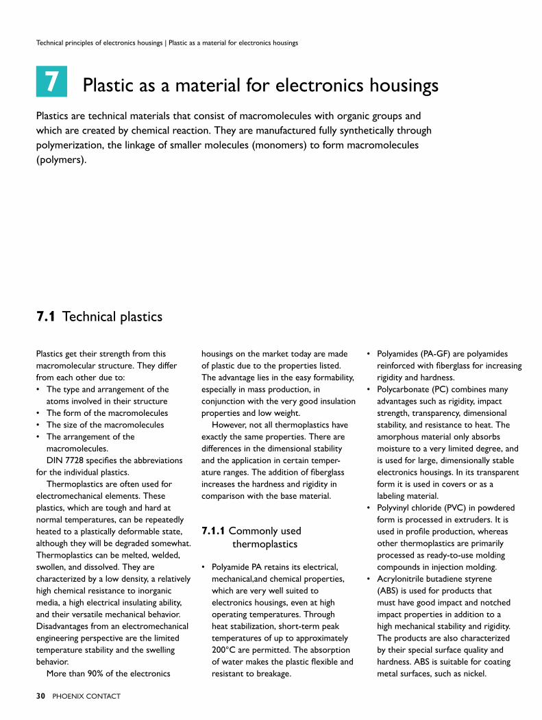
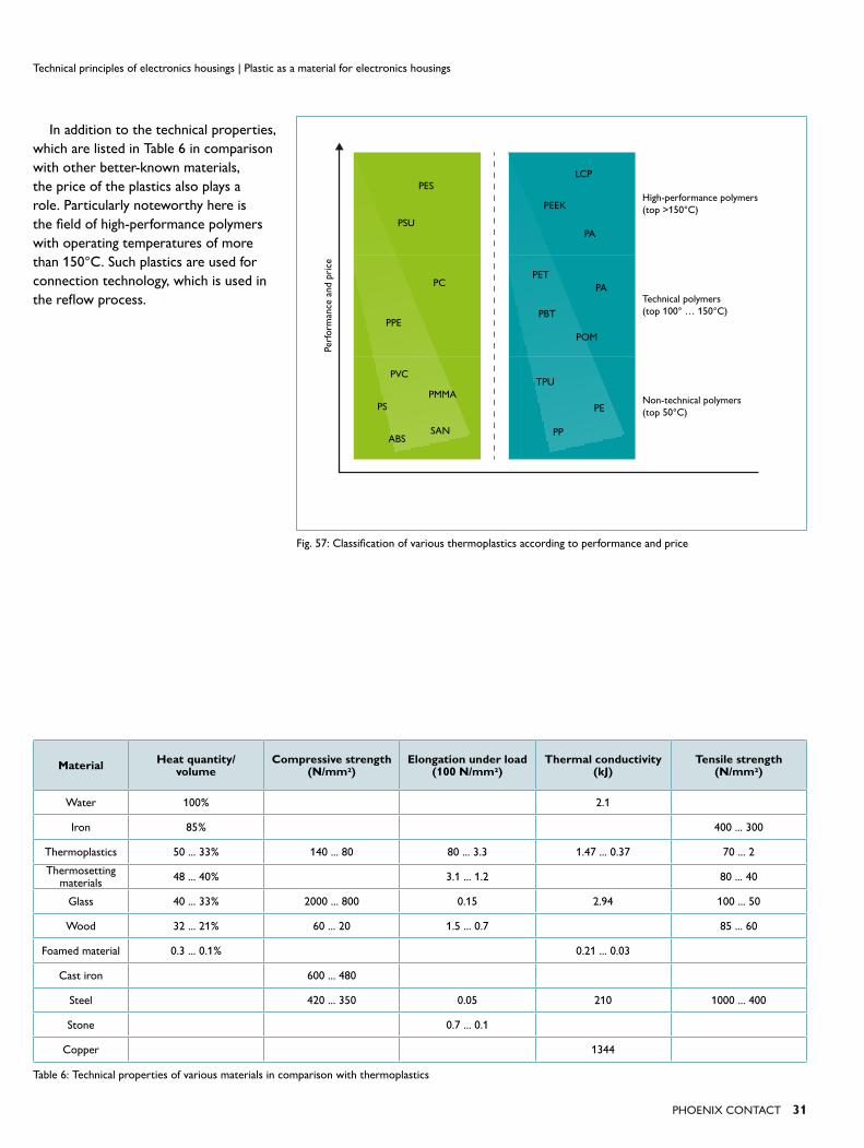
In addition to the technical properties,
which are listed in Table 6 in comparison
with other better-known materials,
the price of the plastics also plays a
role. Particularly noteworthy here is
the fi eld of high-performance polymers
with operating temperatures of more
than 150°C. Such plastics are used for
connection technology, which is used in
the refl ow process.
Table 6: Technical properties of various materials in comparison with thermoplastics
MaterialHeat quantity/
volume Compressive strength
(N/mm2)Elongation under load
(100 N/mm2)Thermal conductivity
(kJ)Tensile strength
(N/mm2)
Water 100% 2.1
Iron 85% 400 ... 300
Thermoplastics 50 ... 33% 140 ... 80 80 ... 3.3 1.47 ... 0.37 70 ... 2
Thermosetting materials
48 ... 40% 3.1 ... 1.2 80 ... 40
Glass 40 ... 33% 2000 ... 800 0.15 2.94 100 ... 50
Wood 32 ... 21% 60 ... 20 1.5 ... 0.7 85 ... 60
Foamed material 0.3 ... 0.1% 0.21 ... 0.03
Cast iron 600 ... 480
Steel 420 ... 350 0.05 210 1000 ... 400
Stone 0.7 ... 0.1
Copper 1344
Technical principles of electronics housings | Plastic as a material for electronics housings
Fig. 57: Classifi cation of various thermoplastics according to performance and price
Per
form
ance
and p
rice
High-performance polymers
(top >150°C)
Technical polymers
(top 100° … 150°C)
Non-technical polymers
(top 50°C)
PES
PSU
PC
PPE
PVC
LCP
PEEK
PA
PET
PA
PBT
POM
TPU
PE
PP
PMMAPS
SANABS
32 PhoEnIx ConTACT
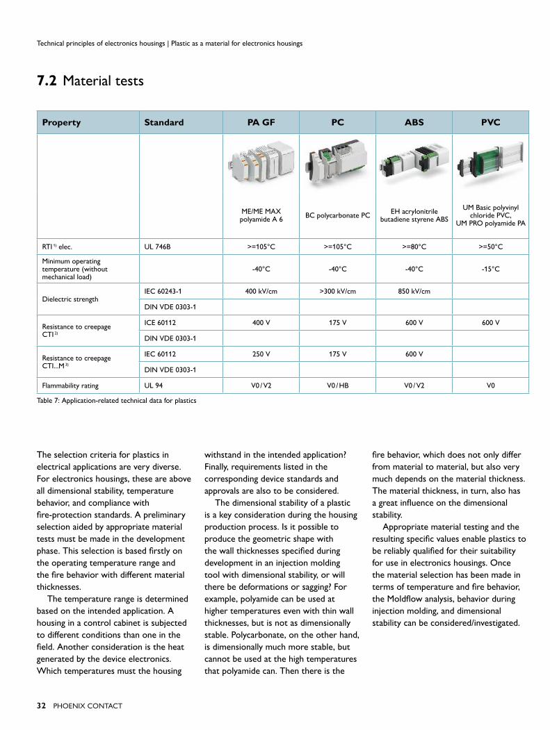
7.2 Material tests
The selection criteria for plastics in
electrical applications are very diverse.
For electronics housings, these are above
all dimensional stability, temperature
behavior, and compliance with
fi re-protection standards. A preliminary
selection aided by appropriate material
tests must be made in the development
phase. This selection is based fi rstly on
the operating temperature range and
the fi re behavior with diff erent material
thicknesses.
The temperature range is determined
based on the intended application. A
housing in a control cabinet is subjected
to diff erent conditions than one in the
fi eld. Another consideration is the heat
generated by the device electronics.
Which temperatures must the housing
withstand in the intended application?
Finally, requirements listed in the
corresponding device standards and
approvals are also to be considered.
The dimensional stability of a plastic
is a key consideration during the housing
production process. Is it possible to
produce the geometric shape with
the wall thicknesses specifi ed during
development in an injection molding
tool with dimensional stability, or will
there be deformations or sagging? For
example, polyamide can be used at
higher temperatures even with thin wall
thicknesses, but is not as dimensionally
stable. Polycarbonate, on the other hand,
is dimensionally much more stable, but
cannot be used at the high temperatures
that polyamide can. Then there is the
fi re behavior, which does not only diff er
from material to material, but also very
much depends on the material thickness.
The material thickness, in turn, also has
a great infl uence on the dimensional
stability.
Appropriate material testing and the
resulting specifi c values enable plastics to
be reliably qualifi ed for their suitability
for use in electronics housings. Once
the material selection has been made in
terms of temperature and fi re behavior,
the Moldfl ow analysis, behavior during
injection molding, and dimensional
stability can be considered/investigated.
Property Standard PA GF PC ABS PVC
ME/ME MAX polyamide A 6
BC polycarbonate PCEH acrylonitrile
butadiene styrene ABS
UM Basic polyvinyl chloride PVC,
UM PRO polyamide PA
RTI 1) elec. UL 746B >=105°C >=105°C >=80°C >=50°C
Minimum operating temperature (without mechanical load)
-40°C -40°C -40°C -15°C
Dielectric strengthIEC 60243-1 400 kV/cm >300 kV/cm 850 kV/cm
DIN VDE 0303-1
Resistance to creepage CTI 2)
ICE 60112 400 V 175 V 600 V 600 V
DIN VDE 0303-1
Resistance to creepage CTI...M 3)
IEC 60112 250 V 175 V 600 V
DIN VDE 0303-1
Flammability rating UL 94 V0 / V2 V0 / HB V0 / V2 V0
Technical principles of electronics housings | Plastic as a material for electronics housings
Table 7: Application-related technical data for plastics

PhoEnIx ConTACT 33
7.2.1 Relative thermal index (RTI)
The relative thermal index (RTI)
in accordance with UL 746B is a
characteristic parameter for the thermal
resistance to aging of a plastic at an
increased temperature. The RTI is defi ned
as the temperature at which a material
(candidate B), when stored in air, lasts for
as long as a comparable other material
(control A) at its already known RTI
temperature, until the value of a specifi c
property has dropped to 50% of its
original value.
There is an RTI value for various
material thicknesses, and typically for the
following characteristics:
• Dielectric strength (RTI Elec.)
• Tensile strength (RTI Str.)
• Impact strength (RTI Imp.)
7.2.2 Resistance to creepage
(CTI, comparative tracking
index)
The resistance to creepage characterizes
the insulation resistance of the surfaces
(creepage distance) of insulation
materials, in particular under the
infl uence of moisture and impurities. It
defi nes the maximum creepage current
which may be set under standardized
test conditions (specifi ed voltage,
conductive layer material) in a defi ned
test arrangement (electrode spacing,
electrode shape).
A high resistance to creepage
means that measurable currents on the
surface of the test piece only occur
when a correspondingly high voltage
(CTI) is applied. The CTI value is only
standardized for voltages of up to 600 V.
The relationship between the
insulation material group and the CTI
value is established in the EN 50124
standard.
The formation of the creepage path
can be caused by contamination of the
surface. The CTI test in accordance
with the IEC/DIN EN 60112 standard
attempts to simulate this by applying a
conductive test solution.
The CTI value is needed for
determining the creepage distances in
accordance with DIN EN 60664. This
standard contains the specifi cations for
insulation coordination for equipment in
low-voltage systems for use at altitudes
up to 2000 m above sea level.
The voltages present, the properties
of the insulation materials (CTI), and
the expected pollution degree are
considered when dimensioning creepage
distances. When determining the
creepage distances, the eff ect of pollution
is considered in accordance with three
degrees of severity. The starting point for
determining the creepage distances is,
however, the rated voltage derived from
the working voltage or nominal mains
voltage. Further diff erentiations are then
made between printed circuits and other
applications. In addition to the creepage
distances, the clearances occurring are
also used for insulation coordination, but
the CTI value does not come into play
here.
Table 8: Insulation material groups in accordance with DIN EN 60664-1
Insulation material group Uprof / V CTI failure criteria
I 600 ≤ CTI
Residual current Ir of≥0.5 A for ≥2 s
Flame forms in ≥2 s
II 400 ≤ CTI < 600
III a 175 ≤ CTI < 400
III b 100 ≤ CTI < 175
Technical principles of electronics housings | Plastic as a material for electronics housings
Fig. 58: Resistance to creepage test
Current measurement
Test piece (≥3 mm)
Drop dispenser
NH4CI
Solution
Test solution A
Power supply
100 ... 600 VacResistance
34 PhoEnIx ConTACT
7.2.3 Hot wire ignition test
(HWI)
In the hot wire ignition test in accordance
with ASTM D 3874, a horizontally
arranged rod-shaped test piece is
wrapped with an electrically heated
resistance wire. This simulates an ignition
source resulting from the overheating
of wires, for example, a coil. The
evaluation criterion for classifi cation in
the fl ammability categories PLC 0 to 5 in
accordance with UL 746 A Section 31 is
the time after which the sample ignites
(0 to 120 seconds). PLC = performance
level category.
7.2.4 High-current arc ignition
test (HAI)
In the high-current arc ignition test in
accordance with UL 746 A Section 32,
a test piece between two electrodes is
exposed to regularly recurring electric
arcs. The HAI value rates the number
of electric arcs up to ignition in the
categories PLC 0 to 4.
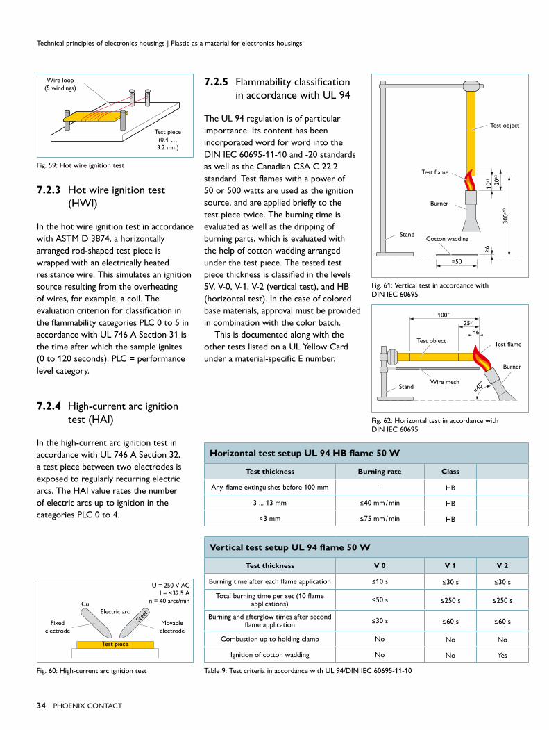
7.2.5 Flammability classifi cation
in accordance with UL 94
The UL 94 regulation is of particular
importance. Its content has been
incorporated word for word into the
DIN IEC 60695-11-10 and -20 standards
as well as the Canadian CSA C 22.2
standard. Test fl ames with a power of
50 or 500 watts are used as the ignition
source, and are applied briefl y to the
test piece twice. The burning time is
evaluated as well as the dripping of
burning parts, which is evaluated with
the help of cotton wadding arranged
under the test piece. The tested test
piece thickness is classifi ed in the levels
5V, V-0, V-1, V-2 (vertical test), and HB
(horizontal test). In the case of colored
base materials, approval must be provided
in combination with the color batch.
This is documented along with the
other tests listed on a UL Yellow Card
under a material-specifi c E number.
Technical principles of electronics housings | Plastic as a material for electronics housings
Fig. 59: Hot wire ignition test
Fig. 60: High-current arc ignition test
Fig. 62: Horizontal test in accordance with
DIN IEC 60695
Fig. 61: Vertical test in accordance with
DIN IEC 60695
Table 9: Test criteria in accordance with UL 94/DIN IEC 60695-11-10
Horizontal test setup UL 94 HB fl ame 50 W
Test thickness Burning rate Class
Any, fl ame extinguishes before 100 mm - HB
3 ... 13 mm ≤40 mm / min HB
<3 mm ≤75 mm / min HB
Vertical test setup UL 94 fl ame 50 W
Test thickness V 0 V 1 V 2
Burning time after each fl ame application ≤10 s ≤30 s ≤30 s
Total burning time per set (10 fl ame applications)
≤50 s ≤250 s ≤250 s
Burning and afterglow times after second fl ame application
≤30 s ≤60 s ≤60 s
Combustion up to holding clamp No No No
Ignition of cotton wadding No No Yes
Wire loop
(5 windings)
Test piece
(0.4 …
3.2 mm)
U = 250 V AC
I = ≤32.5 A
n = 40 arcs/min
Movable
electrode
Fixed
electrode
Test piece
Electric arcCu
Stee
l
Test fl ame
Burner
Test object
StandCotton wadding
≈50
≥6
300
±10
10
±1
20
±2
100±1
25±1
≈6
Test object
Wire meshStand
Test fl ame
Burner
≈45°

PhoEnIx ConTACT 35
7.3 Material certifi cation
Plastics have to be subjected to the above
listed tests before they can be used
in electrical applications. The plastics
themselves are tested, not the housing
made from them. Therefore, test pieces
are used in the tests and not individual
products. The regulations of UL 94
(Underwriters Laboratories) are mainly
used. These have been incorporated into
the DIN IEC 60695-11-10 and -20
standards as well as the Canadian
CSA C 22.2 standard. The results of such
a material test are recorded specifi cally
to the material and manufacturer on
a Yellow Card. These can be used to
look up the behavior of a plastic with
a listed material thickness. Information
on which colors these values apply to is
also to be found here. A Yellow Card can
therefore refer to all colors of a material
or only to the colors listed there. This
does not necessarily mean that other
colors did not pass this test. It may be
that for cost reasons, only a few of the
available colors were tested. Table 10 is
an example of a typical representation of
the characteristic values on such a Yellow
Card.
Color
Minimum material thickness
(mm)
Flammability rating
HWI HAIRTI
Elec.RTI Imp.
RTI Str.
All 0.25 V 0 4 1 65 65 65
0.38 V 0 4 1 130 105 115
0.75 V 0 4 0 130 105 120
1.5 V 0 4 0 130 105 120
3.0 V 0 3 0 130 105 120
Table 10: Typical representation of the material characteristic values for UL-certifi ed plastics

8
36 PhoEnIx ConTACT
8.1 Thermal and mechanical tests
8.1.1 Test for assessing the risk
of fi re
In the glow-wire test in accordance
with DIN EN 60695-2.10:2014-04 or
VDE 0471-2-10:2014-04, the behavior of
an electronics housing is examined under
the direct infl uence of an external ignition
source. The housing must extinguish
itself within a specifi ed period of time.
Furthermore, there must not be a danger
from falling, burning drops.
Housings made of polyamide are
tested at a temperature of 850°C with
an exposure time of 30 s. The time
taken to ignite the test object and to
extinguish the fl ame after removing the
ignition source as well as the number
of falling drops are recorded. The test
is considered passed if the underlay
(tissue paper) does not ignite within the
30 seconds.
8.1.2 Mechanical strength
(tumbling barrel test)
The stability of the fully assembled
housing is tested in the tumbling barrel
test in accordance with DIN EN 60998-1
or VDE 0613-1:2005-03. The focus here
is on latching systems, locking systems,
and screw connections. The housing falls
50 times from a height of 50 cm in the
rotating barrel. The rotation speed is
5 rpm, which equates to 10 drops per
minute.
If the latching systems and locking
systems have not loosened after 50 falls,
and no housing parts have chipped or
broken off , the test is considered passed.
Tests on electronics housings
Once the development of an electronics housing has been completed and the fi rst
pre-series products have been made, the selected properties must be tested in the
laboratory. There are a number of standards to be used as the basis for these tests. In
addition to the material tests and those for the mechanical properties, which were worked
toward during development, tests are still necessary for testing the behavior of the
product under operating conditions.
Technical principles of electronics housings | Tests on electronics housings
Fig. 63: Glow-wire test
Fig. 64: Tumbling barrel test

PhoEnIx ConTACT 37
8.1.3 Test for mechanical seal tightness
In order to be able to make a statement
on the mechanical tightness of the seal
against the ingress of solid bodies and
liquids, the housings are tested based on
the product standard for connectors –
DIN EN 61984 (VDE 0627):2002-9 – and
the results are evaluated in accordance
with DIN EN 60529.
Since housings for mounting on a
DIN rail are usually located in a control
cabinet or a machine, the test for these
housings is limited. These housings are
not expected to be exposed to a dusty
or humid environment.
For fi eld housings that are used
outside the control cabinet, this test
applies in full. The housings are sprayed,
exposed to jet water or even completely
submerged.
Fig. 65: Test for mechanical seal tightness
Table 11: First digit of the IP code
Technical principles of electronics housings | Tests on electronics housings
First digit Description
ISO 20653 DIN EN 60529 Protection against foreign bodies Protection against contact
0 0 No protection No protection
1 1 Protection against solid bodies with a diameter ≥50 mm
Protection against touching with back of hand
2 2 Protection against solid bodies with a diameter ≥12.5 mm
Protection against touching with fi ngers
3 3 Protection against solid bodies with a diameter ≥2.5 mm
Protection against touching with a tool
4 4 Protection against solid bodies with a diameter ≥1.0 mm
Protection against touching with a wire
5K 5 Protection against dustComplete protection against contact
6K 6 Dust-tightComplete protection against contact
Second digit Description
ISO 20653 DIN EN 60529
0 0 No protection
1 1 Protection against dripping water
2 2 Protection against dripping water at a housing tilt angle of 15°
3 3 Protection against spray water up to 60° to the vertical
4 4 Protection against splash water from all directions
4K Protection against splash water with increased pressure from all directions
5 5 Protection against jet water from any angle
6 6 Protection against powerful jet water
6K Protection against powerful jet water with increased pressure, specifi c to road vehicles
7 7 Protection against temporary submersion
8 8 Protection against long-term submersion
9 Protection against water during high-pressure/jet-stream cleaning, especially in agriculture
9K Protection against water during high-pressure/jet-stream cleaning, specifi c to road vehicles
Table 12: Second digit of the IP code
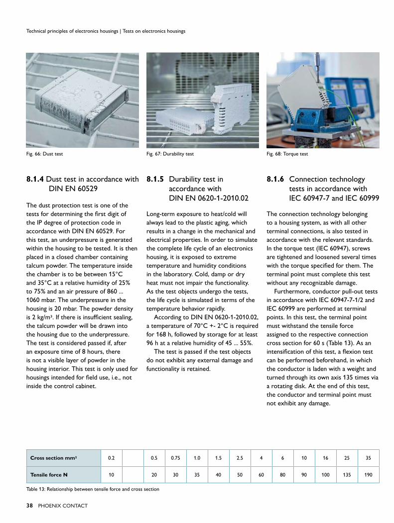
38 PhoEnIx ConTACT
8.1.4 Dust test in accordance with
DIN EN 60529
The dust protection test is one of the
tests for determining the fi rst digit of
the IP degree of protection code in
accordance with DIN EN 60529. For
this test, an underpressure is generated
within the housing to be tested. It is then
placed in a closed chamber containing
talcum powder. The temperature inside
the chamber is to be between 15°C
and 35°C at a relative humidity of 25%
to 75% and an air pressure of 860 ...
1060 mbar. The underpressure in the
housing is 20 mbar. The powder density
is 2 kg/m3. If there is insuffi cient sealing,
the talcum powder will be drawn into
the housing due to the underpressure.
The test is considered passed if, after
an exposure time of 8 hours, there
is not a visible layer of powder in the
housing interior. This test is only used for
housings intended for fi eld use, i.e., not
inside the control cabinet.
8.1.5 Durability test in
accordance with
DIN EN 0620-1-2010.02
Long-term exposure to heat/cold will
always lead to the plastic aging, which
results in a change in the mechanical and
electrical properties. In order to simulate
the complete life cycle of an electronics
housing, it is exposed to extreme
temperature and humidity conditions
in the laboratory. Cold, damp or dry
heat must not impair the functionality.
As the test objects undergo the tests,
the life cycle is simulated in terms of the
temperature behavior rapidly.
According to DIN EN 0620-1-2010.02,
a temperature of 70°C +- 2°C is required
for 168 h, followed by storage for at least
96 h at a relative humidity of 45 ... 55%.
The test is passed if the test objects
do not exhibit any external damage and
functionality is retained.
8.1.6 Connection technology
tests in accordance with
IEC 60947-7 and IEC 60999
The connection technology belonging
to a housing system, as with all other
terminal connections, is also tested in
accordance with the relevant standards.
In the torque test (IEC 60947), screws
are tightened and loosened several times
with the torque specifi ed for them. The
terminal point must complete this test
without any recognizable damage.
Furthermore, conductor pull-out tests
in accordance with IEC 60947-7-1/2 and
IEC 60999 are performed at terminal
points. In this test, the terminal point
must withstand the tensile force
assigned to the respective connection
cross section for 60 s (Table 13). As an
intensifi cation of this test, a fl exion test
can be performed beforehand, in which
the conductor is laden with a weight and
turned through its own axis 135 times via
a rotating disk. At the end of this test,
the conductor and terminal point must
not exhibit any damage.
Table 13: Relationship between tensile force and cross section
Cross section mm2 0.2 0.5 0.75 1.0 1.5 2.5 4 6 10 16 25 35
Tensile force N 10 20 30 35 40 50 60 80 90 100 135 190
Technical principles of electronics housings | Tests on electronics housings
Fig. 68: Torque test Fig. 66: Dust test Fig. 67: Durability test

PhoEnIx ConTACT 39
8.2 Vibration and shock in accordance with DIN EN 60068-2-6 and 60068-2-27
8.2.1 Vibration
For a practical simulation of the vibration
stress, the electronics housings are
subjected to broadband noise-induced
vibrations in all three spatial directions.
The vibration test described in the
IEC 60068-2-6 standard is used for this.
Harmonic, sinusoidal vibrations are
applied to the test object to simulate
rotating, pulsating or oscillating forces.
The test is performed in each of the
three spatial axes (X, Y, Z). The test
is performed over a frequency range
of 10 ... 150 Hz. The acceleration is
5g at an amplitude of 0.35 mm. The
test is considered passed if there is no
visible damage on the housing and no
connections or latching systems have
become loose inside the housing.
8.2.2 Shock
This test is performed to test and
document the resistance of an electronics
housing to shocks of varying energies
occurring at irregular intervals. The
acceleration and duration are specifi ed as
a defi nition of the shock. IEC 60068-2-27
prescribes three positive and negative
shocks in each of the three spatial axes
(X, Y, Z). The simulated accelerations
reach 50 m/s2 with a shock duration of
30 ms. The housings must not exhibit
any damage upon completion of the test.
Special attention is to be focused on
the area of the base latch. In addition,
no individual parts or housing latching
systems must have become loose.
Fig. 69: Vibration test Table 14: Vibration test conditions
Frequency 10 – 150 – 10 Hz
Speed 1 octave/min
Amplitude 0.35 mm
Acceleration 5g
Test duration 2.5 h per axis
Test direction X, Y, and Z axis
Blomberg, Germany
China
USA
Portugal
Spain
FranceSwitzerland
Austria
Italy
Netherlands
Belgium
Luxembourg
Poland
Czech Republic
Slovakia
Hungary
Croatia Romania
United Kingdom
Ireland
Turkey
Israel
UAEVietnam
Philippines
Taiwan, China
Thailand
Singapore
New Zealand
Chile
Argentina
Colombia
CanadaRussia
Finland
Estonia
Latvia
Lithuania
Belarus
Ukraine
Sweden
Norway
Denmark
Kazakhstan
South Korea
Japan
Mexico
Brazil
Australia
Indonesia
Malaysia
India
South Africa
Myanmar
Morocco Cyprus
Uruguay
Slovenia
GreeceMacedonia
MontenegroKosovo
Bosnia andHerzegovina Serbia
Bulgaria Georgia
Azerbaijan
Lebanon
Saudi Arabia
Oman
BahrainQatar
Bangladesh
Honduras
Ecuador
Venezuela
Peru
Bolivia
Paraguay
NicaraguaCosta Rica
Panama
Guatemala
Iceland
Sri Lanka
PakistanKuwait
Iraq
JordanEgypt
Tunisia
Algeria
KenyaUganda
Tanzania
Namibia
Botswana
ZimbabweMozambique
Zambia
NigeriaGhanaCameroon
Mauritius
Moldova
Armenia
Trinidad and Tobago
Dominican Republic
Mongolia
Uzbekistan
PHOENIX CONTACT GmbH & Co. KG
Flachsmarktstraße 8
32825 Blomberg, Germany
Phone: +49 52 35 3-00
Fax: +49 52 35 3-4 12 00
E-mail: [email protected]
phoenixcontact.com
You will fi nd our complete
product range at:
phoenixcontact.com
In dialog with customers and partners worldwide
Phoenix Contact is a globally present, Germany-based market leader. Our group
is synonym for future-oriented components, systems, and solutions in the fi elds of
electrical engineering, electronics, and automation. A global network across more than
100 countries, and 17,400 employees ensure a close proximity to our
customers, which we believe is particularly important.
The wide variety of our innovative products makes
it easy for our customers to fi nd future-oriented
solutions for diff erent applications and industries.
We especially focus on the fi elds of energy,
infrastructure, process and factory automation.
DC
10-1
8.0
01.L
3
MN
R 1
082999/2
019-0
3-0
1/0
0
Pri
nte
d in G
erm
any
© P
HO
EN
IX C
ON
TA
CT
2019