technical paper 022 - flex · tp022: loop compensation and decoupling design with “the loop...
TRANSCRIPT

Loop Compensation And Decoupling Design With “The Loop Compensator”
Technical Paper 022March 2014

TP022: LOOP COMPENSATION AND DECOUPLING DESIGN WITH “THE LOOP COMPENSATOR” 2
ContentsIntroduction 3
Control and system theory 3
The Loop Compensator Load models 7
Control loop design in Loop CompensatorTool 10
Alternative design strategies in Loop Compensator 12
Capacitor decoupling bank design 15
Design examples 15
Fundamental ripple simulation 19
References 20

TP022: LOOP COMPENSATION AND DECOUPLING DESIGN WITH “THE LOOP COMPENSATOR” 3
The introduction of digital control technology in power converters has caused many users to struggle with designing appropriate control loop compensation. A common approach is to use traditional analog tools to determine a solution, and then transform that solution into the digital z-domain. This can be very time consuming and often generates a non-optimal solution. We now present a tool that designs, simulates, analyzes, and configures the power converter directly in the digital z-domain within minutes. Robust design algorithms are added to the Flex Power Designer software to automatically generate optimized solutions, but the design and analysis tools are also available to advanced users. The mathematical model of the power converter is based on the POL of interest and is generated using graph theory and Hamiltonian modeling [7]. The model allows direct design and analysis of digital compensation in the z-domain, simplifying the design process by omitting tedious transformations between the s- and z-domains. The tools also handle design criteria beyond the standard phase and gain margins that ensure proper transient behavior. Tools for capacitor decoupling bank design are also included to minimize the number of capacitors that are necessary for a given load transient performance requirement.
Control And System TheoryIn this section we review the control and system theory that is necessary to understand digital PID (proportional-integral-derivative) control, and provide references for further reading (see the reference list at the end of this document).
Definition of natural frequency and damping ratioThe definition that is used for the natural frequency and damping ratio of a system pole in the Laplace s-plane is illustrated by the complex pole pair in Figure 1, where the natural frequency,ωn , of a pole is the length of the vector from the origin to the pole. While the damping ratio is, the absolute real part of the pole is divided by the length of the vector, i.e. ζ =σ ωn = cos ϕ( ) .
Figure 1. Definitions of natural frequency and damping ratio for a time continuous-time complex-system pole pair.
This means that an undamped system with pure imaginary poles has a damping ratio of zero, and a critically-damped system with a double real pole pair has a damping ratio of one. An over-damped system with two separate poles still has a damping ratio of one. To determine that a system is over-damped, consider the damping ratio and the natural frequency of the poles.
The description of the complex pole pair in the s-domain using the parameters natural frequency and damping ratio becomes:
s1,2 =ωn −ζ ± i 1−ζ2( )
Transformation of poles between continuous- and discrete-time domainsSince the hold circuit for duty cycle is of order 0, i.e. the signal is constant over the switch period, the relationship between the s- and z-domains becomes [8]:
z = e2πsfs
AbstractThis paper describes the Loop Compensator and Capacitor Decoupling Design Tool software for digital DC/DC converters. The DC/DC converter is modeled using a structural flow obtained using graph theory and switched Hamiltonian Differential Algebraic Equation models.
These models are suitable for analysis in the time domain, which is especially useful for load transient simulations. Linear models that can be transformed to the frequency domain for analysis are derived from the Hamiltonian models. The duty cycle is included in the input signal vector, enabling full system analysis with respect to the system’s transfer functions: audio susceptibility, output impedance, and the control loop. These functions are integrated within the “Flex DC/DC Digital Power Designer” software, enabling quick and efficient automated design and analysis of control loop dynamics, load transient behavior, and capacitor decoupling bank requirements. The software includes fundamental ripple simulation.

TP022: LOOP COMPENSATION AND DECOUPLING DESIGN WITH “THE LOOP COMPENSATOR” 4
Analysis of the second-order systemA buck converter with a second-order output filter is shown in Figure 2:
RC = 5mΩ, RL = 10mΩ, C = 150μF, L = 0.9μH
Figure 2. Second order filter buck-converter.
The FETs are modeled as ideal switches, with zero resistance when “On” and open circuit when “Off”. The output filter consists of an inductor L with its parasitic series resistance RL and a capacitor C with its ESR, RESR.
Assuming R= ∞,the unloaded model yields an output LC filter that has a complex pole pair with its angular resonance frequency at ωn =1 LC and a real zero caused by the filter capacitor’s ESR at ωESR =1 RCC .
Hence the control (i.e. duty cycle) to output voltage transfer function is:
H s( ) = s+ωESR
s2 + 2ζrωn +ωn2
where:
ζr =RL + RC2
⎛
⎝⎜
⎞
⎠⎟CL
is the relative damping factor. The component values in Figure 2 yield:
ωn =1LC
⇒ fn =1
2π LC=13.7kHz
ωESR =1RCC
⇒ fESR =1
2πRCC= 212kHz
ζr =RL + RC2
⎛
⎝⎜
⎞
⎠⎟CL= 0.1
The Bode plot of the control transfer function appears in Figure 3. The relative damping factor of 0.1 shows a lowly-damped system with a clearly visible resonance peak at fn =13.7 kHz and 15 dB higher gain than at low frequency. The low damping also yields a rapid phase shift of -180 degrees around the resonance frequency. The ESR zero at fESR = 212kHz starts to increase phase at fESR /10 and reaches a phase lead of 90 degrees at 10 fESR .
Figure 3. Unloaded buck-converter control transfer function.
Because a digital controller sees a sampled version of the buck converter, the model has to be transformed into a discrete-time version. How this is done is shown in detail in reference [7]. A comparison of the continuous-time and discrete-time models appears in Figure 4.
The comparison shows that the magnitude functions overlap almost all the way up to the Nyquist frequency, which is denoted by the vertical black line. Phase shows the same behavior up to the resonance frequency, where the sampled system model shows additional phase lag. Hence, the sampled model is a good representation of the continuous-time model as long as the switching frequency is higher than the system’s dynamic frequencies.
Figure 4. Comparison of time continuous- and discrete-time models of a buck-converter.
A more comprehensive analysis of the control trans-fer function dependency for a complex load and PID design is presented in [9].
−120
−110
−100
−90
−80
−70
−60
Mag
nitu
de (d
B)
100
101
102
−270
−180
−90
0
Pha
se (d
eg)
Bode Diagram
Frequency (kHz)
Time continues systemSampled system
−160
−140
−120
−100
−80
−60
Mag
nitu
de (d
B)
100
101
102
103
104
−180
−135
−90
−45
0
Pha
se (d
eg)
Bode Diagram
Frequency (kHz)

TP022: LOOP COMPENSATION AND DECOUPLING DESIGN WITH “THE LOOP COMPENSATOR” 5
Digital PID implementation theoryThe digital PID regulator is implemented using a second-order Direct form I digital filter as shown in Figure 5, where the second-order feedback signal is omitted:
Figure 5. PID implemented in a second-order Direct form I digital filter.
The integrator is implemented by the feedback in the filter, yielding the transfer function:
I z( ) = 11− z−1
Figure 6 shows the integrator’s Bode plot response:
Figure 6. Bode plot for the integrator.
The magnitude curve increases when the frequency decreases and goes to infinity at DC. This removes regulation error and maintains the output voltage at the steady-state set point. The drawback is the negative phase contribution, from -90 to -180 degrees.
The feed-forward part of the second-order section implements the PD part of PID and has the transfer function:
D z( ) =Ga0 +Ga1z−1 +Ga2z−2 =
=G a0 + a1z−1 + a2z
−2( )
A linear scaling of the three coefficients corresponds directly to changing the gain G in the loop. This leaves three coefficients a0,a1,a2 that correspond to two ze-ros. Assuming two real zeros, the zero with the lowest corresponding natural frequency cancels the integra-tion and flattens the magnitude, while the other zero corresponds to the derivative part that increases the magnitude as frequency increases towards the Nyquist limit. Since the PID is time-discrete, derivative gain does not increase towards infinity due to the periodic property of frequency response for discrete-time sys-tems. As a result, additional high-frequency poles for limiting high-frequency gain are not necessary.
A final factor that has to be accounted for is the delay from sampling the output voltage to starting the next duty cycle, which in this case is modeled as a delay of one switch cycle:
Delay z( ) = z−1
yielding the full transfer function:
PID z( ) =G a0z2 + a1z+ a2z z−1( )
Frequency response is obtained by replacing z = e jωTs , where Ts is the sampling period/switch period:
PID ω( ) =G =G a0ej2ωTs + a1e
jωTs + a2e jωTs e jωTs −1( )
for which the magnitude and phase functions can be obtained.
Analysis of a single real zeroThe magnitude and phase functions for a single real zero with the natural frequency of 1 kHz and sampling frequency of 300 kHz are shown in Figure 7. Magnitude is approximately flat below the zero’s natural frequency and monotonically rising above it.
Phase is positive and approximately 45 degrees at the zero’s frequency, and 0 and 90 degrees at 1/10 and 10 times the zero’s frequency, respectively. Hence, the asymptotic approximations from the continuous-time world apply providing that the sampling frequency is high enough, or at least 10 times higher than the dynamics of interest [8].
−10
0
10
20
30
40
Mag
nitu
de (d
B)
100
101
102
−180
−135
−90
Pha
se (d
eg)
Bode Diagram
Frequency (kHz)

TP022: LOOP COMPENSATION AND DECOUPLING DESIGN WITH “THE LOOP COMPENSATOR” 6
Figure 7. Bode plot for a single real zero.
Compensation Zero placementIn Figure 3 we saw that the complex pole pair contributes a phase lag of -180 degrees around the resonance frequency fn . The zero analysis in previous section Analysis of a single real zero gave us a +45 degree phase lead per real zero near to its natural frequency, reaching +90 degrees at higher frequencies. Hence, we should try to place the zeros at or below the buck converter’s resonance frequency. As a rule-of-thumb we start by placing them at:
fn =13.7 kHz , this yields: z = e2π fnfs = 0.7506
fn 2 = 6.8 kHz , this yields: z = eπ fnfs = 0.8664
This rule-of-thumb yields robust and quite good transient performance. Using a switching frequency of 300 kHz results in discrete-time zeros of z1=0.8664 and z2=0.7506, respectively.
The total PID transfer function becomes:
PID z( ) =Gz− 0.8664( ) z− 0.7506( )
z z−1( )=
=G z2 −1.617z+ 0.6503z z−1( )
The corresponding magnitude and phase functions are shown in Figure 8. The magnitude function shows the usual “PID look” with integration yielding the magnitude increase towards zero frequency, and the derivative gain approaching the Nyquist frequency. Phase starts at -90 degrees due to the integrator and increases around zeros, almost reaching +45 degrees before ending at 0 degrees at the Nyquist frequency, the last -90 degree phase lag coming from the delay.
Figure 8. Bode plot for the PID e jωT( ) .
The open-loop Bode plot of PID e jωT( )H ejωT( ) is shown in Figure 9. The gain is adjusted so the crossover frequency becomes 14 kHz, yielding a gain margin of 11 dB and phase margin of 120 degrees.
Figure 9. Open-loop Bode plot PID e jωT( )H ejωT( ) .
−20
−10
0
10
20
30
40
Mag
nitu
de (d
B)
10−1
100
101
102
−90
−45
0
45
Phas
e (d
eg)
Bode Diagram
Frequency (kHz)
−20
−10
0
10
20
30
40
Mag
nitu
de (d
B)
10−1
100
101
102
−180
−90
0
Pha
se (d
eg)
Bode DiagramGm = 11.2 dB (at 150 kHz) , Pm = 123 deg (at 14 kHz)
Frequency (kHz)
−40
−30
−20
−10
0
10
Mag
nitu
de (d
B)
10−2
10−1
100
101
102
103
0
45
90
135
180
Pha
se (d
eg)
Bode Diagram
Frequency (kHz)

TP022: LOOP COMPENSATION AND DECOUPLING DESIGN WITH “THE LOOP COMPENSATOR” 7
The loop compensator tool can handle two types of external decoupling filters:
1. A two-type capacitor filter.2. A π-filter with two types of capacitors on each side
of the inductor.
Since the external filter becomes part of the system we want to control, it is important to include it within the model.
The two-type capacitor filterThe first simple model that can be used when the distance between the power module and the load is short is shown in Figure 10. The model also includes a resistance Rwire for modeling the copper trace resistance between the module, the decoupling capacitors, and the load on the motherboard. Two different types of capacitors are included in the model. This is in most cases enough for loop design, as all the other capacitance and ESR values are well outside the bandwidth of the loop and serve as high-frequency noise filters.
Figure 10. DC/DC converter model with external two-type capacitor decoupling.
Capacitor decoupling descriptionThe simplest way to determine which capacitors to include in the design tool is to calculate and sort them by:
> Total capacitane per type Cx−tot =CxNx , and > Longest time constant: τ x = ESRx ⋅Cx
The two capacitor types that have the largest total capacitance and longest time constants should be included in the design. The other capacitors’ time constants are usually so small that they will not interfere with the control loop, or can be handled using margins for additional component/model uncertainty.
A decoupling capacitors exampleA typical mix of capacitors in a decoupling capacitor bank is shown in Table 1. Three large-value capacitors act as the bulk smoothing component but have rather high ESR values. These capacitors are often accompanied by smaller capacitors that are most often ceramic types, which have small capacitance values but much lower ESR. In order to attenuate noise over a wide range of frequencies, typically many different values of ceramics are used in parallel with the bulk component.
# of cap Capaci-tance[µF]
ESR[mΩ]
Tot C:[µF]
Time constant
[ns]
3 470 10 1410 4700
15 100 5 1500 500
10 22 5 220 110
100 1 15 100 15
100 0.1 20 10 2
Table 1: A mix of capacitors in a decoupling capacitor bank.
Which capacitors shall we include in the Loop Compensator tool for our design? Looking at the first two rows, the bulk 470 µF capacitors and the 100µF ceramics have the largest total capacitance and also happen to have the longest time constants. Hence, these two capacitor arrays should be included in the design.
Capacitor derating and tolerance handlingCapacitors are often derated due to physical variables such as temperature and DC-voltage. Read the capacitor’s datasheet carefully and use the derated values as typical values. In the component tolerance values, include not only the normal specifications but also any derating data.
The PI-filter descriptionIn some applications, small ceramics are used in such large numbers that they start to influence the low frequency control-loop domain. This requires a model of higher order. In other applications, watch for parasitic elements such as from using inductors/ferrite beads in filters. Or, it may be possible that the distance between the power module and the load is sufficient to make trace inductance large enough to interfere with the control loop. The filter model that covers these applications is shown in Figure 11. The filter has two capacitor types close to the power module, CM1 and CM2, followed by an inductor L with its parasitic resistance RACR. The trace resistance Rwire is included in series, and at the load side two other
The Loop Compensator Load Models

TP022: LOOP COMPENSATION AND DECOUPLING DESIGN WITH “THE LOOP COMPENSATOR” 8
capacitor types are located, CL1 and CL2 where NM1 number of capacitors in parallel of type CM1 yields the total capacitance for that type of CM1NM1 and the total ESR of ESRM1/NM1. This is also valid for the other three capacitors, CM2, CL1, and CL2.
Figure 11. PI-filter model with two types of capacitors on each side of the inductor.
Paralleling PI-filtersIn another application, one power module is supplying several loads in parallel. The model for this scenario is shown in Figure 12 for K loads in parallel. Usually they share the common bulk capacitor bank located close to the power module, here modeled by using two types of capacitors, CM1 CM2. Each load has its own local decoupling bank, consisting of two types of capacitors CL1k and CL2k and connects to the bulk capacitors via an inductor, Lk.
Figure 12. Several PI-filters in parallel with common capacitors close the power module.
Assume the loads are shorted together, i.e. all the inductors Lk and capacitors CL1k and CL2k are parallel-coupled. Further assume using only two types of capacitors for local decoupling at the loads, i.e. CL1 =CL1k and CL2 =CL2k for all k. This can be simulated using the single PI-filter shown in Figure 13:
Figure 13. Modularity simplifies the parallel in Figure 12 filter can be simplified.
The corresponding number of each capacitor type is simply:NLT1
= N11 + N12 +...N1KNLT 2
= N21+ N22
+...N2K
Assuming K identical inductors, the effective inductance L and parasitic resistance RACR becomes: L = L1 /KRACR = ACR /K
If the K different PI-filters are identical, this simplification is no approximation. But if the PI-filters are not identical, the approximation error can be minimized by sensing the output voltage at the branch with the largest capacitance.
PI-filter capacitor choices and placementCM1 Bulk capacitorsTThe purpose of the bulk capacitors is to cover the low-frequency range between where the power module stops working (~30 KHz) and the high-frequency capacitors start to work (~1 MHz). Bulk capacitors can be large and difficult to place very close to the load. Fortunately, this is not a problem because the low-frequency energy covered by bulk capacitors is not sensitive to capacitor location. They can be placed almost anywhere on the PCB, but the best placement is as closely as possible to the load, which is also where the power modules should be placed. Capacitor mounting should follow normal PCB layout practices, tending toward short and wide shapes connecting to power planes through multiple vias. Recommended bulk capacitors are OS-Con, Pos-cap, or polymer aluminum electrolytics.
CM2 large ceramics, size 1210The 100 µF 1210 capacitors cover the low/middle frequency range. If a larger inductor is used in the PI-filter, these capacitors become critical for handling the ripple current from the power module because the inductor efficiently blocks ripple currents.
CL1 large ceramics, size 1206 or 0805The 47 µF capacitors in 1206 or 0805 sizes cover the middle frequency range. Placement has some impact on performance. Capacitors should be placed as closely as possible to the load. Any placement within 50 mm of the load’s outer edge is acceptable.
CL2 small ceramics, size 0805 or 0603The 10 µF capacitors in size 0805 or 0603 cover the middle/high frequency range. Again, these capacitors should be placed as closely as possible to the load. Any placement within 25 mm of the load’s outer edge is acceptable.
Additional ceramics, size 0402For example, 0.47 µF 0402 capacitors cover the high-frequency range. Placement and mounting are critical for these components. Capacitors must be mounted as closely to the load as possible (to minimize parasitic

TP022: LOOP COMPENSATION AND DECOUPLING DESIGN WITH “THE LOOP COMPENSATOR” 9
inductance). For PCBs with a thickness of ~1.5-1.6 mm, the best location is on the PCB backside within the load’s footprint. VCC and GND vias corresponding to the supply of interest should be identified in the via array. Where space is available, 0402 mounting pads should be added and connected to these vias.
For thicker PCBs, the depth of the VCC plane of interest in the PCB stack-up is the key factor; if the VCC plane is in the PCB stack-up’s top half, capacitor placement on the top surface is optimal; similarly if the VCC plane is in the PCB stackup’s bottom half, capacitor placement on the bottom surface of the PCB is best. Any 0402 capacitors placed outside the device footprint (whether on the top or bottom surface) should be within 10-15 mm of the load’s outer edge.
Number of capacitors of each typeThe number of capacitors of each type shall be chosen to obtain a flat impedance curve. The number of bulk capacitors that have high ESR is not that critical as they are efficient over a large frequency band and do not cause anti-resonance spikes, i.e. where the ESL in the larger capacitor starts to oscillate with the smaller capacitor.
For ceramic capacitors with low ESR, the number used is more critical: a flat response is obtained if the total number of capacitors of each type/size is doubled when the capacitance of each type decreases. An example is shown in the table:
Type Capacitance[µF]
Number of capacitors
Total capacitance
[µF]
CM1 470 1 470
CM2 100 5 500
CL1 47 10 470
CL2 10 20 200
Table 2: Example of mixed capacitors in the output filter.
If the impedance is too high or if the load transient requirement cannot be fulfilled, increase the number of bulk capacitors NM1 by one. If that does not fulfill the requirements, scale the number of ceramics by the same factor. The Decoupling Bank design tool will assist you with this task, see section Capacitor decoupling bank design (page 15).
Capacitor mounting and solder landsThe capacitor mounting (solder pads, traces, and vias) should be optimized for low inductance. Vias should be butted directly against the pads, see Figure 14.
Vias can be located at the ends of the pads (a) but are better located at the sides of the pads, (b). Via place-ment at the sides of the pads decreases the mounting’s overall parasitic inductance by increasing the mutual inductive coupling of one via to the other. Dual vias can be placed on both sides of the pads for even lower parasitic inductance (c) but with diminishing returns. If micro-vias are used, they can be placed within the pads for further reducing inductance (d).
Figure 14. Example capacitor pads and via placements.
Loop compensator capacitor descriptionThe description of the capacitors in the Loop Compensator tool is shown in Figure 15. Here, we can fill in the component’s typical value together with its tolerance, or minimum and maximum values for capacitance and ESR:
Figure 15. Load capacitor description.

TP022: LOOP COMPENSATION AND DECOUPLING DESIGN WITH “THE LOOP COMPENSATOR” 10
System analysis and component tolerancesWhile it is simple to calculate the number of capacitors and check datasheets for typical capacitance and ESR values, the tolerance of these values is often large - usually several tens of percent. The Loop Compensation tool calculates all the corner cases for the powertrain filter. That data can be used in the PID design by placing the compensation zeros to ensure a robust, high-performance design.
All corner cases are evaluated and each system’s two dominant poles (natural frequency and damping ratio) are calculated and presented as shown in Figure 16. The DC/DC converter model in Figure 10 is fourth-order. The tool identifies the two dominant poles using Hankel singular values [8] and reports the result for the reduced and approximated second order system.
For the Integration and Derivative parts, the Loop Compensator tool uses a zero placement strategy rather than traditional tuning of time parameters.
Open-loop frequency design and requirementsThe standard tool for open-loop design is the Bode plot in Figure 17, in which we can place the compensation zeros to obtain proper behavior and adjust gain to fulfill the robustness requirements in terms of phase and gain margins. Common values for these requirements are 60 degrees and 6 dB.
The tool plots the typical system, analyzes all corner systems, and plots the systems with the minimum and maximum values for phase and gain margin. If all de-sign requirements are fulfilled, a green Loop signal to-gether with the word “Stable” is displayed in the upper left corner, providing a quick answer for loop stability. If one or both of the phase and gain margin requirements are not fulfilled, the color changes to red and the text reads “Unstable”, see Figure 17.
Closed loop design and requirementsSince we have a discontinuous-time system, phase and gain margins alone are insufficient to ensure proper DC/DC converter behavior. This cannot be observed in the open-loop Bode plot but becomes obvious in the closed-loop version, see Figure 18.
Figure 16. Analysis of system resonance frequency and damping.
Figure 17. Open-loop Bode plot.
Control Loop Design in Loop Compensator Tool
TP022: LOOP COMPENSATION AND DECOUPLING DESIGN WITH “THE LOOP COMPENSATOR” 11
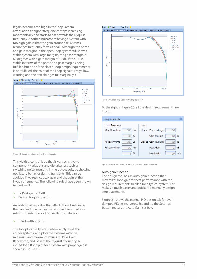
If gain becomes too high in the loop, system attenuation at higher frequencies stops increasing monotonically and starts to rise towards the Nyquist frequency. Another indicator of having a system with too high gain is that the gain around the system’s resonance frequency forms a peak. Although the phase and gain margins in the open-loop system still show a stable system with large margins, the phase margin is 60 degrees with a gain margin of 10 dB. If the PID is stable in terms of the phase and gain margins being fulfilled but one of the closed-loop design requirements is not fulfilled, the color of the Loop signal turns yellow/warning and the text changes to “Marginally”:
Figure 18. Closed-loop Bode plot with too high gain.
This yields a control loop that is very sensitive to component variations and disturbances such as switching noise, resulting in the output voltage showing oscillatory behavior during transients. This can be avoided if we restrict peak gain and the gain at the Nyquist frequency. The following rules have been shown to work well:
> LoPeak gain < 1 dB > Gain at Nyquist < -6 dB
An additional key value that affects the robustness is the bandwidth, which in the past has been used as a rule-of-thumb for avoiding oscillatory behavior:
> Bandwidth < fs/10.
The tool plots the typical system, analyzes all the corner systems, and plots the systems with the minimum and maximum values for Peak Gain, Bandwidth, and Gain at the Nyquist frequency. A closed-loop Bode plot for a system with proper gain is shown in Figure 19.
Figure 19. Closed-loop Bode plot with proper gain.
To the right in Figure 20, all the design requirements are listed:
Figure 20. Loop Compensation and Load Transient requirements tab.
Auto-gain functionThe design tool has an auto-gain function that maximizes loop gain for best performance with the design requirements fulfilled for a typical system. This makes it much easier and quicker to manually design zero placements.
Figure 21 shows the manual PID design tab for over-damped PID i.e. real zeros. Expanding the Settings button reveals the Auto Gain set box.

TP022: LOOP COMPENSATION AND DECOUPLING DESIGN WITH “THE LOOP COMPENSATOR” 12
Figure 21. Control loop PID, Over Damped manual design tab with Auto Gain enabled.
Robustness analysisThe tool analyzes the design margins in the worst-case corners for a typical system and presents the results, see Figure 22. In addition to the loop’s key parameters, audio susceptibility (input to output voltage transfer function), and load impedance transfer functions are calculated and their peak values are presented. This helps check the robustness of the design.
Alternative Design Strategies in Loop CompensatorDefault control loop stability checkThe first thing you may want to do is check if the de-fault control loop (i.e. the PID settings that the product is delivered with) is good enough in terms of stability and load transient performance.
Start by entering your requirements (see Figure 20) and the load description (see Figure 15). The next step is to verify that the PID taps have their default values. In Figure 23, the PID taps are shown to the right. When the values are gray and in Italic the values are defaults:
Figure 23. Control Loop Tab, with default PID taps.
The final step is to check the indicators that appear above the Bode plots, see Figure 24. In this case, the control loop is fully stable with all requirements fulfilled, but one or more load transient requirement is not fulfilled:
Figure 24. Check of stability and load transient requirement fulfilment.
The designer now has a choice between redesigning the capacitor decoupling or changing the PID responses to try to fulfil all the design requirements. The following sections explain several different PID design options.
Basic control loop designA common rule-of-thumb for placing zeros that is robust for modeling error or component variations and yields good transient behavior is:
> Place the first compensation real zero at the system’s typical resonance frequency.
> Place the second real zero one octave below the first zero.
Figure 22. Robustness analysis - key parameters.

TP022: LOOP COMPENSATION AND DECOUPLING DESIGN WITH “THE LOOP COMPENSATOR” 13
This is implemented in the design tool for a simple and robust design, which will in many cases be adequate. Simply change the control loop type to Basic, see Figure 25, and click on the Set button. The Autoset Rule can also be changed from the default values, these values being reached by expanding Control Loop, Settings.
The natural frequency for the PID zeros follows these equations:
NF Zero 1= Typical system pole 2× Autoset Rule LowNF Zero 2 = Typical system pole 2× Autoset Rule High
where the natural frequency for the typical system pole 2 can be found in the System result tab, see Figure 16. The auto-gain function is also used to automatically maximize the gain.
Figure 25. Control loop PID Basic design tab.
Over-damped/real zeros compensation designIf the Basic Over-damped control design did not fulfill the design requirements, you may want to tweak the real zeros manually. This is easily accomplished by changing the control type to Over Damped, see Figure 26. In this way, you can change the natural frequencies of the zeros independently of one other. By default the auto-gain function is on. It can be switched off by expanding Settings, see Figure 21.
Figure 26. Control loop Tab, with Over-damped compensation.
Under-damped compensation/complex zero compensationThe digital PID allows for the use of a complex zero pair, i.e. under-damped compensation. Change the control type to “Under damped” as shown in Figure 27.
Figure 27. Control loop tab, with Under-damped compensation.
This can be used to cancel out the complex system pole pair, i.e. exact cancellation. However, this is generally not recommended due to high sensitivity toward modeling error or system variations. In case of a mismatch, the margins for stability decrease rapidly and result in an oscillatory system.
In some cases, it can still be good to evaluate under-damped compensation. A common case is when ceramic capacitors are exclusively used in the decoupling network. Since ceramics have the property of small capacitance and low ESR, it becomes necessary to use many in parallel and the powertrain tends to be very lowly damped. The following rule-of-thumb can maximize the robustness of under-damped compensation. Place the complex zero pair inside the worst-case system poles, which can be stated as:
> Place the zeros at the minimum natural frequency of the system poles.
> Use the maximum damping. Alternatively, the load transient optimization that next section describes for real zeros often finds a solution with similar performance, but is less sensitive to modeling error.
Load transient optimizationIn the case of a known system, the load transient performance can be optimized by placing the compensation zeros differently from the rule-of-thumb, described in previous section Basic control loop design.
Since the optimal zero placements vary with the system’s properties and the optimization problem is small, exhaustive search is easily applied with
TP022: LOOP COMPENSATION AND DECOUPLING DESIGN WITH “THE LOOP COMPENSATOR” 14
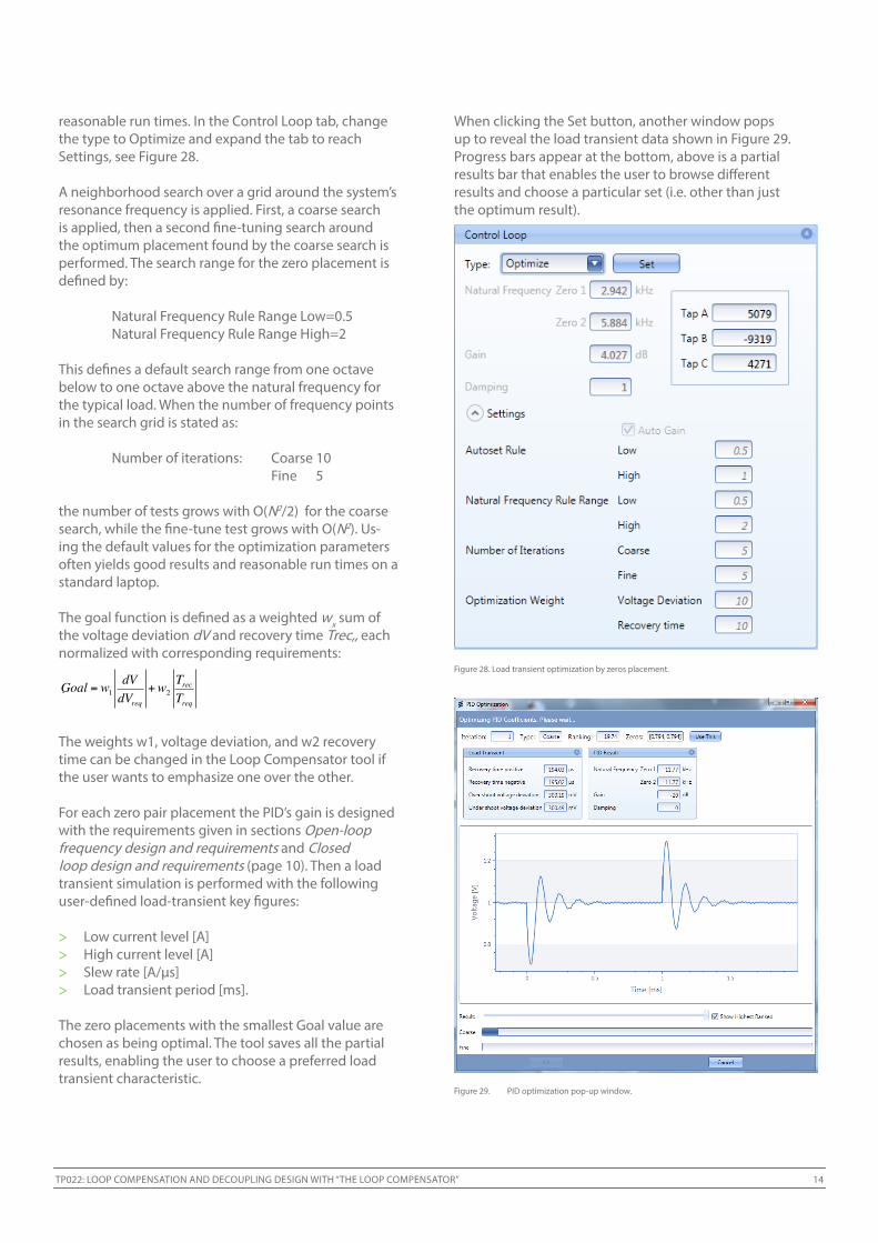
reasonable run times. In the Control Loop tab, change the type to Optimize and expand the tab to reach Settings, see Figure 28.
A neighborhood search over a grid around the system’s resonance frequency is applied. First, a coarse search is applied, then a second fine-tuning search around the optimum placement found by the coarse search is performed. The search range for the zero placement is defined by:
Natural Frequency Rule Range Low=0.5 Natural Frequency Rule Range High=2
This defines a default search range from one octave below to one octave above the natural frequency for the typical load. When the number of frequency points in the search grid is stated as:
Number of iterations: Coarse 10 Fine 5
the number of tests grows with O(N2/2) for the coarse search, while the fine-tune test grows with O(N2). Us-ing the default values for the optimization parameters often yields good results and reasonable run times on a standard laptop.
The goal function is defined as a weighted wx sum of the voltage deviation dV and recovery time Trec,, each normalized with corresponding requirements:
Goal = w1dVdVreq
+w2TrecTreq
.
The weights w1, voltage deviation, and w2 recovery time can be changed in the Loop Compensator tool if the user wants to emphasize one over the other.
For each zero pair placement the PID’s gain is designed with the requirements given in sections Open-loop frequency design and requirements and Closed loop design and requirements (page 10). Then a load transient simulation is performed with the following user-defined load-transient key figures:
> Low current level [A] > High current level [A] > Slew rate [A/µs] > Load transient period [ms].
The zero placements with the smallest Goal value are chosen as being optimal. The tool saves all the partial results, enabling the user to choose a preferred load transient characteristic.
When clicking the Set button, another window pops up to reveal the load transient data shown in Figure 29. Progress bars appear at the bottom, above is a partial results bar that enables the user to browse different results and choose a particular set (i.e. other than just the optimum result).
Figure 28. Load transient optimization by zeros placement.
Figure 29. PID optimization pop-up window.

TP022: LOOP COMPENSATION AND DECOUPLING DESIGN WITH “THE LOOP COMPENSATOR” 15
The tool can also assist in the design of the capacitor decoupling bank by determining the number of capacitors needed to fulfill the load transient requirement. The tools use a divide-and-conquer approach to determine the minimum decoupling bank, which yields a O(log(N) time for arriving at the result. This is an iterative process where you optimize one capacitor type at a time. By clicking on the “Optimize” button in Figure 30, a pop-up window shown in Figure 31 opens for the capacitor type that you want to optimize. The max value is the maximum number of capacitors in parallel that the optimization will attempt.
Figure 30. The capacitor description with Optimize click button.
Example 1: Compensation of a system, low damping A BMR462 with 5 pieces of 100 µF ceramic capacitors with ESR = 4 mΩ as a load yields the system parameters shown in Figure 32:
Figure 32. Parameters for a lowly-damped system.
Using an exact cancellation approach for the typical system yields the open-loop Bode plot in Figure 33. The magnitude curve for the typical load becomes a straight line, i.e. a perfect integration whereas extreme systems deviate at frequencies above resonance. The phase curve for the typical system shows an almost straight line at -90 degrees, yielding a phase margin of 90 degrees. Deviations from the typical load reduce that margin to 66 degrees.
The closed-loop Bode plot in Figure 34 shows perfect behavior for the typical load, i.e. a straight line up to its bandwidth limit and monotonically decreasing gain above that point. By contrast, systems that deviate from the typical system show resonance below and above the typical system’s bandwidth.
Capacitor Decoupling Bank DesignAt the bottom a progress bar is shown with color-coded results. When the optimization completes, click on the “Use This” button.
Figure 31. Capacitor optimization pop-up window.
Design Examples
TP022: LOOP COMPENSATION AND DECOUPLING DESIGN WITH “THE LOOP COMPENSATOR” 16
Figure 33. Open-loop Bode plot with exact cancellation of the typical load.
Figure 34. Closed-loop Bode plot using exact cancellation of the typical load.
Looking at only these two Bode plots, the system should behave very well. However, examining load transient we see that oscillatory behavior occurs, yielding a large second overshoot of 40 mV for the typical system and up to 46 mV worst-case.
Figure 35. Load transient obtained using exact cancellation for the typical system.
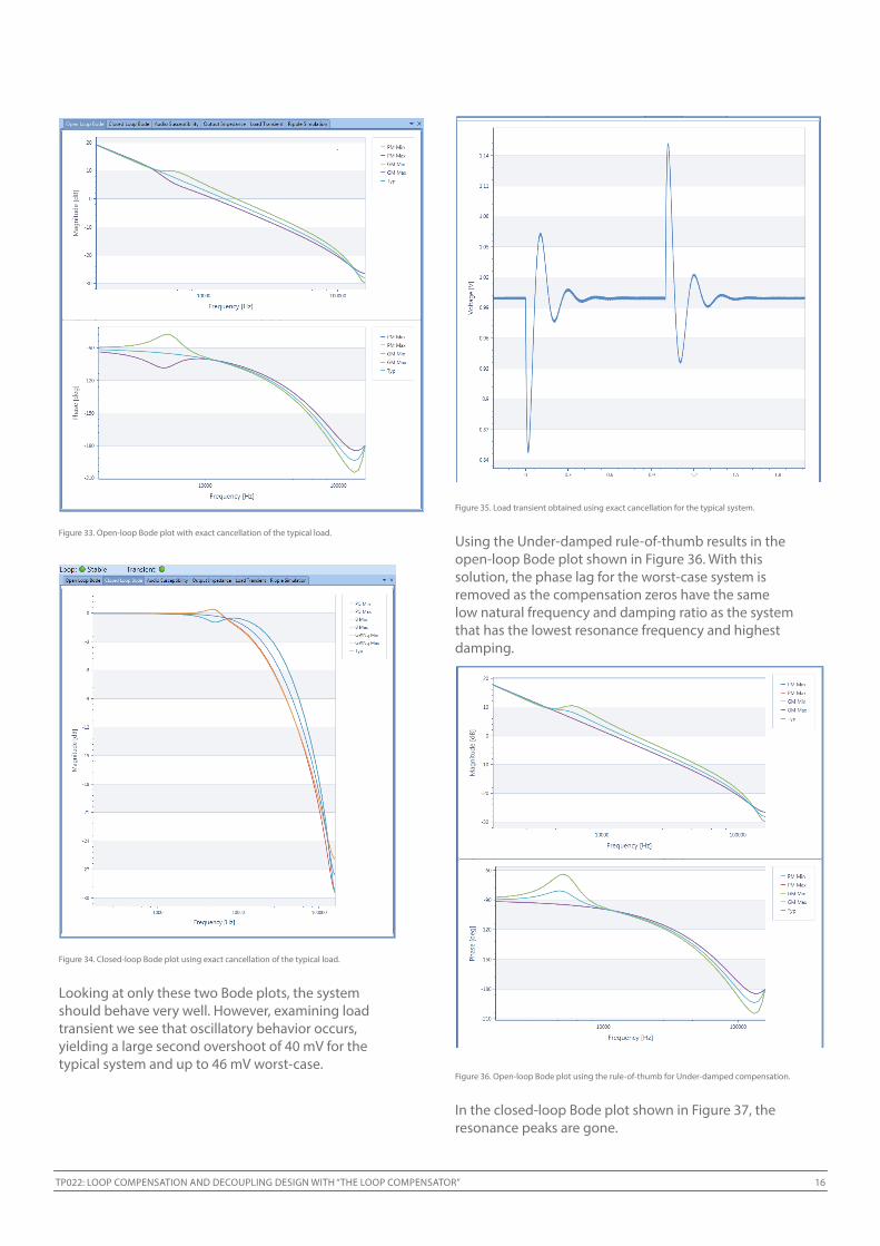
Using the Under-damped rule-of-thumb results in the open-loop Bode plot shown in Figure 36. With this solution, the phase lag for the worst-case system is removed as the compensation zeros have the same low natural frequency and damping ratio as the system that has the lowest resonance frequency and highest damping.
Figure 36. Open-loop Bode plot using the rule-of-thumb for Under-damped compensation.
In the closed-loop Bode plot shown in Figure 37, the resonance peaks are gone.

TP022: LOOP COMPENSATION AND DECOUPLING DESIGN WITH “THE LOOP COMPENSATOR” 17
Figure 37. Closed-loop Bode plot using the rule-of-thumb for Under-damped compensation.
This looks promising for the load transient shown in Figure 38. The secondary overshoots are reduced to 31 mV for the typical system and 35 mV worst-case.
Figure 38. Load transient obtained using the rule-of-thumb for Under-damped compensation.
By comparison, using the Basic over-damped rule-of-thumb yields the load transient in Figure 39, where the oscillatory behaviour is almost gone.
Figure 39. Load transient obtained using the rule-of-thumb for Basic Over-damped compensation.
Comparison of the load transient performance where the recovery limit is 30 mV is shown in Table 3:
Compensa-tion type
Recovery time
positive [µs]
Recovery time
positive [µs]
Over Voltage
deviation[mV]
Under Voltage
deviation [mV]
Exact cancellation
128 127 109 111
Rule-of-thumb under
damped cancellation
125 120 110 112
Basic over damped rule-of-thumb
49 50 124 127
Optimized overdamped
46 45 118 120
Table 3: Comparison of load transient key results for different types of loop compensation.
The voltage deviations for the over-damped compensations show half the recovery time compared with the under-damped compensation. This is due to the virtually non-existent oscillatory behavior that results from using over-damped compensation, meantime voltage deviations have increased from 110 mV to 120 mV. The over-damped compensation optimization does not find a much better solution.
How this optimization is performed is described in the next section.
TP022: LOOP COMPENSATION AND DECOUPLING DESIGN WITH “THE LOOP COMPENSATOR” 18
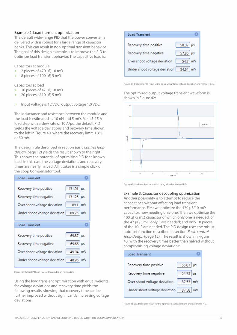
Example 2: Load transient optimizationThe default wide-range PID that the power converter is delivered with is robust for a large range of capacitor banks. This can result in non-optimal transient behavior. The goal of this design example is to improve the PID to optimize load transient behavior. The capacitive load is:
Capacitors at module > 2 pieces of 470 µF, 10 mΩ > 8 pieces of 100 µF, 5 mΩ
Capacitors at load > 10 pieces of 47 µF, 10 mΩ > 20 pieces of 10 µF, 5 mΩ
> Input voltage is 12 VDC, output voltage 1.0 VDC.
The inductance and resistance between the module and the load is estimated as 10 nH and 5 mΩ. For a 5-15 A load step with a slew rate of 10 A/µs, the default PID yields the voltage deviations and recovery time shown to the left in Figure 40, where the recovery limit is 3% or 30 mV.
The design rule described in section Basic control loop design (page 12) yields the result shown to the right. This shows the potential of optimizing PID for a known load, in this case the voltage deviations and recovery times are nearly halved. All it takes is a simple click of the Loop Compensator tool:
Figure 40. Default PID and rule-of-thumb design comparison.
Using the load transient optimization with equal weights for voltage deviations and recovery time yields the following results, showing that recovery time can be further improved without significantly increasing voltage deviations.
Figure 41. Optimized PID result using equal weights for voltage deviation and recovery time.
The optimized output voltage transient waveform is shown in Figure 42:
Figure 42. Load transient simulation using a load-optimized PID.
Example 3: Capacitor decoupling optimizationAnother possibility is to attempt to reduce the capacitance without affecting load transient performance. First we optimize the 470 µF/10 mΩ capacitor, now needing only one. Then we optimize the 100 µF/5 mΩ capacitor of which only one is needed; of the 47 µF/5 mΩ only 5 are needed; and only 10 pieces of the 10uF are needed. The PID design uses the robust auto-set function described in section Basic control loop design (page 12) . The result is shown in Figure 43, with the recovery times better than halved without compromising voltage deviations:
Figure 43. Load transient result for the optimized capacitor bank and optimized PID.

TP022: LOOP COMPENSATION AND DECOUPLING DESIGN WITH “THE LOOP COMPENSATOR” 19
The tool simulates fundamental ripple using a resistive load that consumes the current described in the Load description tab shown in Figure 44:
Figure 44. Load description including the load current used in the ripple simulation.
In the first example, two pieces of 470 µF/10 mΩ ca-pacitors are used for decoupling and result in the ripple shown in Figure 45. The resulting fundamental ripple becomes 9.17 mV peak-to-peak.
Figure 45. Ripple simulation using two capacitors.
A PI-filter can be built by adding an inductor of just 10 nH/1 mΩ between the two capacitors. The PI-filter ripple simulation is shown in Figure 46. The sharp edges shown in Figure 45 are gone and the ripple amplitude is reduced to 4.46 mV peak-to-peak. For the same ripple to be obtained using only capacitors, 6 pieces of 470µF/10 mΩ are required.
Figure 46. Ripple simulation using a PI-filter.
Hence, a PI-filter is very efficient for reducing ripple. However, load transient behavior suffers from increased recovery times and voltage deviations even with the optimized PID settings shown in Figure 47, where the 6-piece capacitor filter’s load transient figures are shown to the left and the corresponding key figures for the PI-filter to the right. Hence, the voltage deviations are almost tripled while recovery times are increased by around 70 percent.
Figure 47. Comparison of load transients, at the top, 6 pieces of capacitors versus, below, PI-filter, with two capacitors.
Fundamental Ripple Simulation

TP022: LOOP COMPENSATION AND DECOUPLING DESIGN WITH “THE LOOP COMPENSATOR” 20
[1] R. Ortega, A. Loria, P. J. Nicklasson, and H. Sira-Ramirez, Passivity-based Control of Euler-Lagrange Systems, Springer, 1998.[2] A. van der Schaft, L2-Gain and Passivity Techniques in Nonlinear Control, Springer, 2000.[3] D. B West, Introduction to graph theory, Prentice Hall, 2001.[4] W. P. M. H Heemels, M. K. Camlibel, A. J. van der Schaft, and J. M. Schumacher, “Modeling, wellposedness and stability of switched electrical networks,” Lecture notes in computer science, vol 2623, pp. 249-266. Springer-verlag, 2003.[5] R. D. Middlebrook, and S. Cuk, “A General Unified approach to modeling switching converter power stages,” IEEE Power Electronics Specialists Conference Record, PESC-76, pp. 18-34, 1976.[6] B. Johansson, “DC-DC Converters, Dynamic Model Design and Experimental Verification,” Dissertation LUTEDX/(TEIE- 1042)/1-194/(2004), Dep. Of Industrial Electrical Engineering and Automation, Lund University, Lund, 2004.[7] M. Karlsson, T. Holmberg, A. Hultgren, and M. Lenells, ”Structural Modeling Flow of Switched Electrical Networks,” DPF’09, Sept. 21-23, Santa Ana, CA, USA, 2009.[8] T. Glad, and L. Ljung, Control theory, 1 ed., CRC, 2000.[9] M. Karlsson, T. Holmberg, and M. Lenells, “Analysis of a Capacitive Loaded Buck Converter,” in Proc. of the International Telecommunications Energy Conference 2009, INTELEC’09, Songdo/Incheon, Republic of Korea, Oct., 2009.,
References

TP022: LOOP COMPENSATION AND DECOUPLING DESIGN WITH “THE LOOP COMPENSATOR” 21
The content of this document is subject to revision without notice dueto continued progress in methodology, design and manufacturing.Flex shall have no liability for any error or damage of any kindresulting from the use of this document
Flex Power Modulesflex.com/expertise/power/modules
TECHNICAL PAPER1/287 01-CXC 173 5018 R1A
© Flex Dec 2017
Flex Power Modules Torshamnsgatan 28 A164 94 Kista, SwedenEmail: [email protected]
Flex Power Modules - Americas600 Shiloh RoadPlano, Texas 75074, USATelephone: +1-469-229-1000
Flex Power Modules - Asia/PacificFlex Electronics Shanghai Co., Ltd 33 Fuhua Road, Jiading DistrictShanghai 201818, ChinaTelephone: +86 21 5990 3258-26093